Electronic energy levels and energy relaxation mechanisms in self-organized InAs/GaAs quantum dots M. J. Steer,* D. J. Mowbray, ² W. R. Tribe, ‡ M. S. Skolnick, and M. D. Sturge § Department of Physics, University of Sheffield, Sheffield S3 7RH, United Kingdom M. Hopkinson, A. G. Cullis, and C. R. Whitehouse Engineering and Physical Sciences Research Council Central Facility for III-V Semiconductors, Department of Electronic and Electrical Engineering, University of Sheffield, Sheffield, S1 3JD, United Kingdom R. Murray Department of Material Science and Engineering, University of Liverpool, Liverpool, L69 3BX, United Kingdom ~Received 28 May 1996! We report a spectroscopic investigation of the electronic energy levels and carrier-relaxation mechanisms in self-organized InAs/GaAs quantum dots. Power-dependent photoluminescence ~PL! and photoluminescence excitation ~PLE! are used to study the energy-level structure. Two excited states, 74 and 120 meV above the luminescent ground state, are identified. As expected for a zero-dimensional system, it is not possible to observe PL from the ground state of the dots when exciting between the energies of the ground and first excited state due to the discrete, atomiclike nature of the electronic states. Selectively excited PL and PLE reveal two mechanisms for the relaxation of carriers from the excited states to the ground state: a nonresonant mechanism dominant in the upper state, and a resonant mechanism, involving the emission of one or more LO phonons of well-defined energy, which is dominant in the lower excited state. The resonant mechanism is shown to be a consequence of the distribution of energy-level spacings in the inhomogeneous ensemble of dots; preferentially selecting dots with an energy-level spacing close to an integer multiple of the LO phonon energy. @S0163-1829~96!02548-9# I. INTRODUCTION Quantum dots provide the ultimate quantum system with three-dimensional carrier confinement resulting in atomic- like, discrete electronic energy states. In addition to allowing the study of physics in a zero-dimensional semiconductor system, these discrete energy levels are expected to result in a number of advantageous properties for electronic and electro-optic device applications. Quantum dot lasers are pre- dicted to exhibit both low threshold current densities, 1 and low- or zero-temperature dependence of the threshold current, 1 while the use of quantum dots may offer possibili- ties for low-power nonlinear devices. However, for device applications to be a realistic prospect the quantum dots must satisfy a number of requirements. These include large carrier confinement and energy-level separations @kT , large areal densities, high optical quality, and uniform size and shape. Of the many techniques proposed and investigated for the fabrication of quantum dots, perhaps the most promising is that of self-organized growth. 2–5 Dots prepared by this tech- nique appear to be capable of satisfying all of the above requirements, although further improvements in size and shape uniformity are desirable. Self-organized growth may occur when a thin layer of one semiconductor is grown epi- taxially on a second semiconductor of a different lattice con- stant. For intermediate values of lattice mismatch the initial two-dimensional growth transforms, above a certain critical thickness, to nonuniform three-dimensional growth, resulting in a spatial modulation of the epitaxial layer thickness. This is known as the Stranski-Krastanov growth mechanism. The small areas of three-dimensional growth, which sit on a thin two-dimensional layer ~the so-called wetting layer!, form the quantum dots. Although initially observed in the InAs-on- GaAs system, self-organized dots have now been observed in a wide range of material systems. 4,6,7 For the InAs-on-GaAs system, for which there is a 7% lattice mismatch, the result- ant InAs dots have a typical base size ;10–25 nm and height ;2–10 nm, 2,8 the actual size being dependent to some extent upon the growth conditions. These dimensions are small enough that strong quantum effects are observed. In this paper we present a study of the electronic energy levels and carrier relaxation mechanisms in self-organized InAs/GaAs quantum dots. The latter topic is of particular importance in zero-dimensional systems since it has been predicted that their discrete, atomiclike energy levels may inhibit the efficient carrier relaxation by single phonon emis- sion, which occurs in systems with continuous energy levels. 9 Unless other efficient relaxation mechanisms are possible, i.e., multiphonon, 10 Auger, 11 or long-range reso- nance energy transfer, 12 carrier relaxation rates will be very slow, with serious implications for device performance. II. EXPERIMENTAL DETAILS The samples were grown by solid source molecular-beam epitaxy using conditions very similar to those of Moison et al. 2 The structure consisted of a thin layer of InAs depos- ited on a GaAs buffer layer, which in turn was grown on an undoped GaAs substrate. At the growth temperature used ~T g 5500–520 °C! the transformation from two- to three- PHYSICAL REVIEW B 15 DECEMBER 1996-II VOLUME 54, NUMBER 24 54 0163-1829/96/54~24!/17738~7!/$10.00 17 738 © 1996 The American Physical Society

Welcome message from author
This document is posted to help you gain knowledge. Please leave a comment to let me know what you think about it! Share it to your friends and learn new things together.
Transcript
PHYSICAL REVIEW B 15 DECEMBER 1996-IIVOLUME 54, NUMBER 24
Electronic energy levels and energy relaxation mechanismsin self-organized InAs/GaAs quantum dots
M. J. Steer,* D. J. Mowbray,† W. R. Tribe,‡ M. S. Skolnick, and M. D. Sturge§
Department of Physics, University of Sheffield, Sheffield S3 7RH, United Kingdom
M. Hopkinson, A. G. Cullis, and C. R. WhitehouseEngineering and Physical Sciences Research Council Central Facility for III-V Semiconductors,
Department of Electronic and Electrical Engineering, University of Sheffield, Sheffield, S1 3JD, United Kingdom
R. MurrayDepartment of Material Science and Engineering, University of Liverpool, Liverpool, L69 3BX, United Kingdom
~Received 28 May 1996!
We report a spectroscopic investigation of the electronic energy levels and carrier-relaxation mechanisms inself-organized InAs/GaAs quantum dots. Power-dependent photoluminescence~PL! and photoluminescenceexcitation~PLE! are used to study the energy-level structure. Two excited states, 74 and 120 meV above theluminescent ground state, are identified. As expected for a zero-dimensional system, it is not possible toobserve PL from the ground state of the dots when exciting between the energies of the ground and first excitedstate due to the discrete, atomiclike nature of the electronic states. Selectively excited PL and PLE reveal twomechanisms for the relaxation of carriers from the excited states to the ground state: a nonresonant mechanismdominant in the upper state, and a resonant mechanism, involving the emission of one or more LO phonons ofwell-defined energy, which is dominant in the lower excited state. The resonant mechanism is shown to be aconsequence of the distribution of energy-level spacings in the inhomogeneous ensemble of dots; preferentiallyselecting dots with an energy-level spacing close to an integer multiple of the LO phonon energy.@S0163-1829~96!02548-9#
iticintoulanpr
oili-ceurri
ethg-ovnapontiacainhiTh
hin
n-d in
ult-
eare
rgyzedlareenayis-gyre
amns-ansed-
I. INTRODUCTION
Quantum dots provide the ultimate quantum system wthree-dimensional carrier confinement resulting in atomlike, discrete electronic energy states. In addition to allowthe study of physics in a zero-dimensional semiconducsystem, these discrete energy levels are expected to resa number of advantageous properties for electronicelectro-optic device applications. Quantum dot lasers aredicted to exhibit both low threshold current densities,1 andlow- or zero-temperature dependence of the threshcurrent,1 while the use of quantum dots may offer possibties for low-power nonlinear devices. However, for deviapplications to be a realistic prospect the quantum dots msatisfy a number of requirements. These include large caconfinement and energy-level separations@kT, large arealdensities, high optical quality, and uniform size and shap
Of the many techniques proposed and investigated forfabrication of quantum dots, perhaps the most promisinthat of self-organized growth.2–5 Dots prepared by this technique appear to be capable of satisfying all of the abrequirements, although further improvements in size ashape uniformity are desirable. Self-organized growth moccur when a thin layer of one semiconductor is grown etaxially on a second semiconductor of a different lattice cstant. For intermediate values of lattice mismatch the initwo-dimensional growth transforms, above a certain critithickness, to nonuniform three-dimensional growth, resultin a spatial modulation of the epitaxial layer thickness. Tis known as the Stranski-Krastanov growth mechanism.
540163-1829/96/54~24!/17738~7!/$10.00
h-grt inde-
ld
ster
.eis
edyi--llgse
small areas of three-dimensional growth, which sit on a ttwo-dimensional layer~the so-called wetting layer!, form thequantum dots. Although initially observed in the InAs-oGaAs system, self-organized dots have now been observea wide range of material systems.4,6,7 For the InAs-on-GaAssystem, for which there is a 7% lattice mismatch, the resant InAs dots have a typical base size;10–25 nm andheight;2–10 nm,2,8 the actual size being dependent to somextent upon the growth conditions. These dimensionssmall enough that strong quantum effects are observed.
In this paper we present a study of the electronic enelevels and carrier relaxation mechanisms in self-organiInAs/GaAs quantum dots. The latter topic is of particuimportance in zero-dimensional systems since it has bpredicted that their discrete, atomiclike energy levels minhibit the efficient carrier relaxation by single phonon emsion, which occurs in systems with continuous enerlevels.9 Unless other efficient relaxation mechanisms apossible, i.e., multiphonon,10 Auger,11 or long-range reso-nance energy transfer,12 carrier relaxation rates will be veryslow, with serious implications for device performance.
II. EXPERIMENTAL DETAILS
The samples were grown by solid source molecular-beepitaxy using conditions very similar to those of Moisoet al.2 The structure consisted of a thin layer of InAs depoited on a GaAs buffer layer, which in turn was grown onundoped GaAs substrate. At the growth temperature u~Tg5500–520 °C! the transformation from two- to three
17 738 © 1996 The American Physical Society
iois
bthth
wn
-
rsuid
wmuml
ie
ith
K
ieh
a
inggatm
tsur
sethhe-obs
h
th
isilarnso
tatesis
ant
cu-otsof
o aandforthes.lec-ndc-ntynot
his
ex-rumof
e-
ple
54 17 739ELECTRONIC ENERGY LEVELS AND ENERGY . . .
dimensional growth was found to occur after the depositof a nominal 1.8–1.9 ML of InAs. However, x-ray analysof samples containing an InxGa12xAs/GaAs multiple-quantum-well buffer suggests that the InAs thickness may;5–10 % lower than intended due to In desorption atgrowth temperature used. The main sample studied inpaper consisted of 2.4 ML~nominal! of InAs, which resultedin square quantum dots of base length'12 nm, height'2nm, and density;531010 cm22, as evidenced by plan viewand cross-sectional transmission electron microscopy.13 Thegrowth was terminated with the InAs dots being overgroby a GaAs capping layer of thickness 100 nm.
Photoluminescence~PL! and high-resolution photoluminescence excitation~PLE! spectra were excited with an Ar1
pumped Ti: sapphire laser and the resultant PL was dispeby a double-grating spectrometer and detected with a liqnitrogen-cooled Gep- i -n photodiode. Low-resolution PLEspectra were obtained over a wider energy range and at loincident power density with a 150-W tungsten halogen laand monochromator combination. In both cases a large nber of dots~;108 dots for laser excitation with a cylindricafocusing lens illuminating an area'231023 cm2 and;1010
dots for lamp and monochromator excitation of an area'0.1cm2! were probed. Higher incident laser power densit;50–5000 W cm22 were obtained with a micro-PL systemthat uses a HeCd laser~lex5440 nm excitation! and a high-quality microscope objective to give a laser spot size;1–2mm. Most of this short-wavelength excitation is absorbedthe GaAs capping layer resulting in strong excitation ofdots ~;1 e-h pair per dot at 50 W cm22!. All the measure-ments were performed with a sample temperature of 4.2
III. EXPERIMENTAL RESULTS
The quantum dot samples exhibit very strong PL at'1.1mm, for excitation both above and below the GaAs barrband gap. We compared their PL efficiency to that of higquality 10- and 20-Å GaxIn12xAs-InP quantum wells, whichemit in the same wavelength region and are believed to hvery high luminescent efficiency.14 For both types of struc-ture the excitation was directly into the active region usphotons of an energy less than that of the barrier bandThe integrated PL intensity of the dot sample was foundbe a factor;10 weaker than that of the individual quantuwells. However, given that the dots occupy only;5% of thetotal sample area, the absolute quantum efficiencies ofdots and the quantum wells are comparable. This resultgests that the dots do not introduce a significant numbenonradiative recombination pathways.
Figure 1 shows PL spectra as a function of incident lapower, using the high-power densities obtainable withmicro-PL system. If we assume a radiative lifetime for tdots of;1 ns,15 no lateral carrier diffusion within the wetting layer away from the excited region and that all the phtoexcited carriers produced in the GaAs barriers are suquently captured by the dots, the lowest power of 45 W cm22
is calculated to produce a dot occupancy;1. At this powerwe observe only a single peak at 1.13 eV, labeledT1. Wewill refer to this as the ‘‘ground-state’’ transition. The widtof this peak~35 meV at the lowest power! results from varia-tions in the size and shape, and hence variation in
n
eeis
ed-
erp-
s
ne
.
r-
ve
p.o
heg-of
re
-e-
e
ground-state energy, of the dots probed. This linewidthsomewhat smaller than values previously reported for simsamples,3,5,16indicating that these size and shape fluctuatioare reasonably small@a 35-meV PL linewidth corresponds tbase length variations of'60.5 nm ~Ref. 17!#. With in-creasing laser power density the intensity of the ground-semission approximately saturates and additional featureT2and T3 are observed to higher energies. This behaviorattributed to the filling of the ground state and the resultrecombination from excited states.18,19
The nature of the excited dot states is unclear with callations of the electronic structure of self-organized InAs dgiving conflicting results. For example, the calculationsGrundmann, Stier, and Bimberg17 for pyramidal dots predictonly one confined electron state, with allowed transitions tnumber of heavy-hole states. On the other hand, MarzinBastard20 predict at least two confined electron statescone-shaped dots. A possible cause of this discrepancy isdifferent choice of effective mass for the electronCapacitance-voltage measurements, which distinguish etron from hole states, by Medeiros-Ribeiro, Leonard, aPetroff21 on '20-nm-diameter InAs dots indicate two eletron states but only one hole state. In view of this uncertaiconcerning the electronic structure of the dots we canreliably identify the states involved with the transitionsT2and T3. The conclusions reached in the remainder of tpaper are independent of such identification.
Although PLE has been used extensively to study thecited states of quantum wells, the observed PLE spectonly represents the absorption spectrum if the probabilityrelaxation from the initially excited state to the ground~lu-minescing! state is independent of energy. Any energy d
FIG. 1. Power-dependent PL spectra of the quantum dot samexcited with short-wavelength light~lex54420 Å[2.80 eV!.
Inrowctcthocect o
thLOhisoro
bicfioibewitee
-
usingit isthethen.ab-toLE
ingablethatndring
-
the3,be-rgy.in
ithent
ThonP
asthede-
17 740 54M. J. STEERet al.
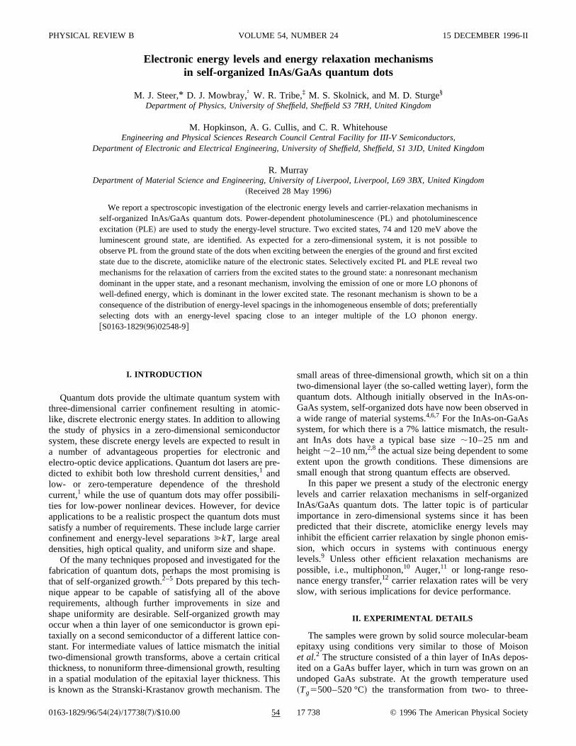
pendence of this probability will distort the spectrum.quantum wells this is generally a weak effect and PLE pvides reliable excited-state transition energies. However,find that in our quantum dots the carrier relaxation efficienis a function of energy, showing strong resonances whenenergy separation between the incident photon and deteenergies is equal to certain integer multiples of the LO pnon energy. This energy dependence dominates the speso that excited-state energies cannot be determined dirfrom the spectra. This behavior is shown in the main parFig. 2, which shows PL~excited at 1.291 eV! and PLE~de-tected at 1.14 eV, the peak of the PL! of the sample, bothrecorded with laser excitation. The absolute energies ofsharp features in the PLE spectrum, labeled 2LO and 3depend upon the detection energy, shifting rigidly as tenergy is varied~see Fig. 3 below!. Hence the peak positiondo not give the excited-state energies, and we will shbelow that they appear to represent the effects of carrierlaxation by the emission of two or more LO phononswell-defined energy.
For energies below the phonon features~&1.17 eV! thePLE signal falls to zero. This indicates that no measuraPL is produced when exciting in this energy range, whcorresponds to energies between the ground state andexcited state of the dots being probed. Such behavior is csistent with that expected for a zero-dimensional system wdiscrete, atomiclike energy levels. Although light mayabsorbed directly into the ground state of the dots andsubsequently be reemitted, for a zero-dimensional systhis should occur at the same energy as that of the incid
FIG. 2. PL and PLE spectra obtained using laser excitation.inset shows a typical PLE spectrum recorded using lamp and mchromator excitation. For both PLE spectra detection is at themaximum.
-eyheion-tra,tlyf
e,s
we-f
lehrstn-th
llmnt
photons~zero Stokes shift!, so long as the dots are sufficiently far apart that no transfer between dots occurs.22 Suchresonant ground-state emission has not been observedour present experimental techniques, probably becauseobscured by the elastically scattered laser light fromsample surface or by resonant Rayleigh scattering frominhomogeneously broadened ground-state transitio23
Hence, for the present experimental conditions, only bysorbing into an excited state, from which relaxation occursthe lower-energy emitting ground state, can a nonzero Psignal be obtained.
The inset to Fig. 2 shows a PLE spectrum recorded usthe lamp and monochromator combination, which allowsmuch wider energy range to be scanned than is availawith the laser. For low energies the spectrum agrees withobtained with the laser. At higher energies the lamp amonochromator PLE spectrum shows absorption occurinto both the two-dimensional InAs wetting layer~'1.4–1.5eV! and the GaAs barrier layers~'1.52 eV!. The featuresoccurring at'1.29 and'1.37 eV are briefly discussed below.
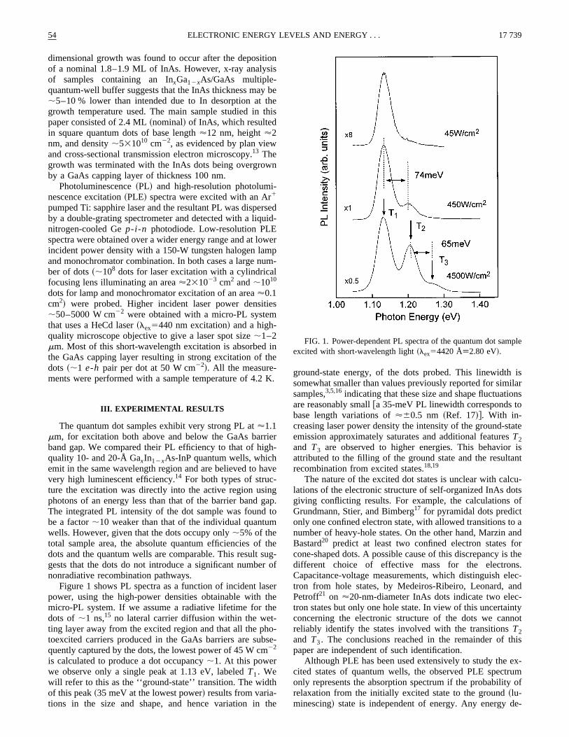
The behavior of the features labeled 2LO and 3LO inPLE spectrum of Fig. 2 is shown in more detail in Fig.which shows PLE spectra plotted against the differencetween the incident photon energy and the detection eneSpectra are shown for detection at three different pointsthe PL peak shown in the inset~recorded for an excitationenergy of 1.291 eV!. The PLE spectra show three peaks wconstant shifts from the detection energy. For the pressample these energy shifts are 58~2329!, 84~3328!, and
eo-L
FIG. 3. PLE spectra obtained for different detection energiesindicated in the inset. The spectra are plotted as a function ofenergy difference between the incident photon energy and thetection energy.
ondisinth
a
ifyinbl-otLOtLth
faoct,
geatdbbdo
oain
lehionAse
coietsbun
ned
ioa
Gelap
LOB
theirso-Lctra
ver,ith
ndareLthesetheirnonPLhatachthex-
ainndfera-the
ofthesrgy
54 17 741ELECTRONIC ENERGY LEVELS AND ENERGY . . .
102~3334! meV, respectively. The unstrained LO phonenergy of InAs is 29.9 meV and the calculations of Grunmann, Stier, and Bimberg17 suggest that strain increases thvalue to 32.1 meV in pyramidal-shaped dots. In the wettlayer a slight reduction to 29.6 meV is predicted, due tocompeting effects of strain and confinement.17 Hence thefeatures observed in the PL and PLE spectra occur atproximately two~2LO! and three~3LO! multiples of theseInAs LO phonon energies. We therefore tentatively identthem as being due to carrier relaxation processes involvthe emission of two or three LO phonons. Although possitwo 3LO features~84 and 102 meV! are present in the spectra of Fig. 3, which may indicate the coupling of the delectronic states to both the dot and wetting layerphonons, only one 2LO feature is observed. However, ipossible that the 2LO feature corresponding to the weak 3feature at 102 meV is obscured by the low-energy tail ofdominant 3LO feature at 84 meV.
The present results are analogous to those of Faet al.,18 where strong features shifted by a single LO phonfrom the excitation energy were observed in the PL speof Al xIn12xAs/AlxGa12xAs self-organized quantum dotsand those of Heitzet al.16 for InAs/GaAs dots similar toours. However, the sample of Ref. 16 had a slightly larPL linewidth~45 meV!,16 and a peak was observed in PLEthe single~1LO! phonon energy in addition to the 2LO an3LO features observed in the present sample. As willexplained later, the phonon features are believed to arisecause the experiment selects out of the ensemble ofhaving a range of energy-level separations,16 those dots forwhich this separation is an integral number of LO phonenergies. In our relatively homogeneous samples, the smest energy separation is presumably greater than the sLO phonon energy.
Heitz et al.16 also observed substructure in their multipphonon peaks, as measured in resonantly excited PL, wthey attributed to coupling to various different phonmodes including interface, dot, wetting layer, and Gaphonons. Such substructure is not observed in the presample. The very sharp lines observed at;35 meV are Ra-man lines. These have energies of 33.7 and 36.5 meV,responding to the bulk GaAs TO and LO phonon energrespectively, and do not show significant resonance effecthe energy region of the dot states. They thus representGaAs phonons that are not coupled to the dot electrostates.
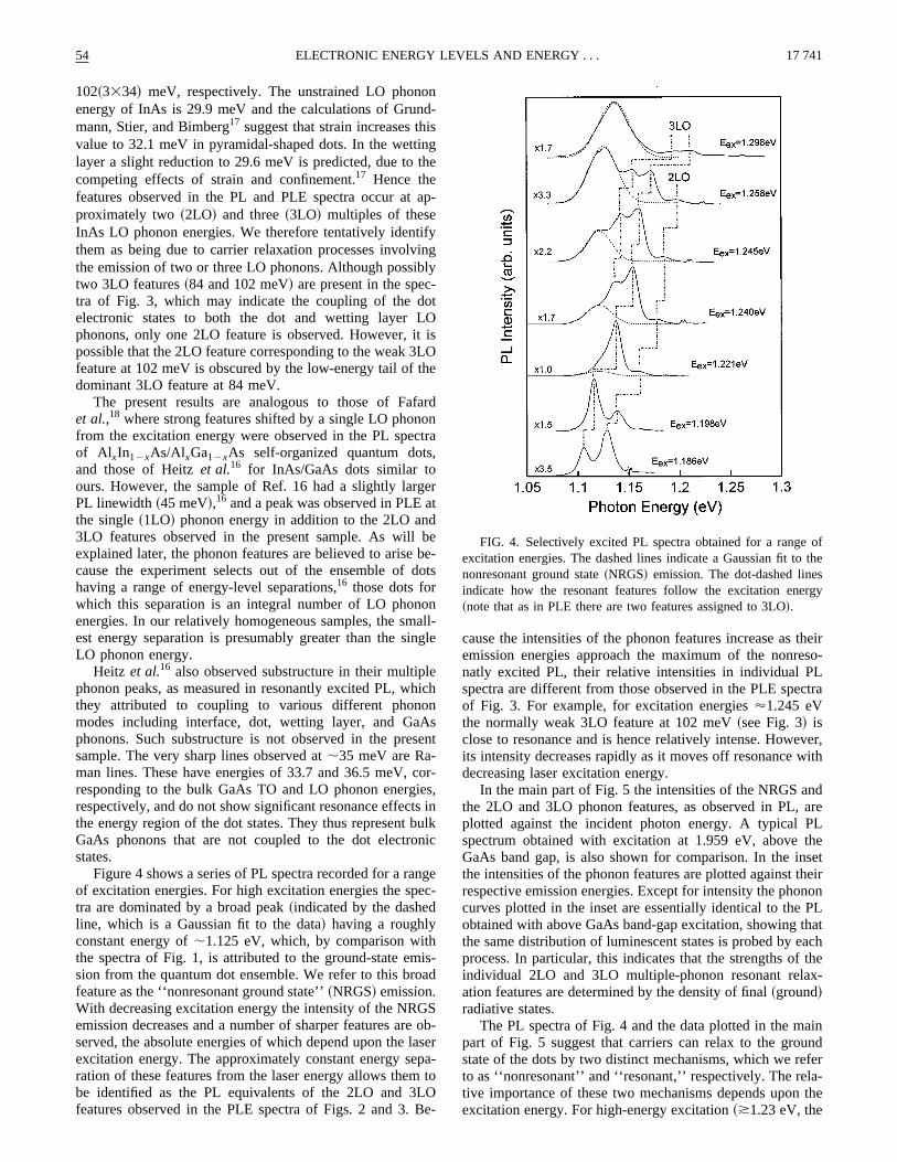
Figure 4 shows a series of PL spectra recorded for a raof excitation energies. For high excitation energies the sptra are dominated by a broad peak~indicated by the dasheline, which is a Gaussian fit to the data! having a roughlyconstant energy of;1.125 eV, which, by comparison withthe spectra of Fig. 1, is attributed to the ground-state emsion from the quantum dot ensemble. We refer to this brfeature as the ‘‘nonresonant ground state’’~NRGS! emission.With decreasing excitation energy the intensity of the NRemission decreases and a number of sharper features arserved, the absolute energies of which depend upon theexcitation energy. The approximately constant energy seration of these features from the laser energy allows thembe identified as the PL equivalents of the 2LO and 3features observed in the PLE spectra of Figs. 2 and 3.
-
ge
p-
gy
isOe
rdnra
r
ee-ts
nll-gle
ch
snt
r-s,inlkic
gec-
s-d
Sob-sera-to
e-
cause the intensities of the phonon features increase asemission energies approach the maximum of the nonrenatly excited PL, their relative intensities in individual Pspectra are different from those observed in the PLE speof Fig. 3. For example, for excitation energies'1.245 eVthe normally weak 3LO feature at 102 meV~see Fig. 3! isclose to resonance and is hence relatively intense. Howeits intensity decreases rapidly as it moves off resonance wdecreasing laser excitation energy.
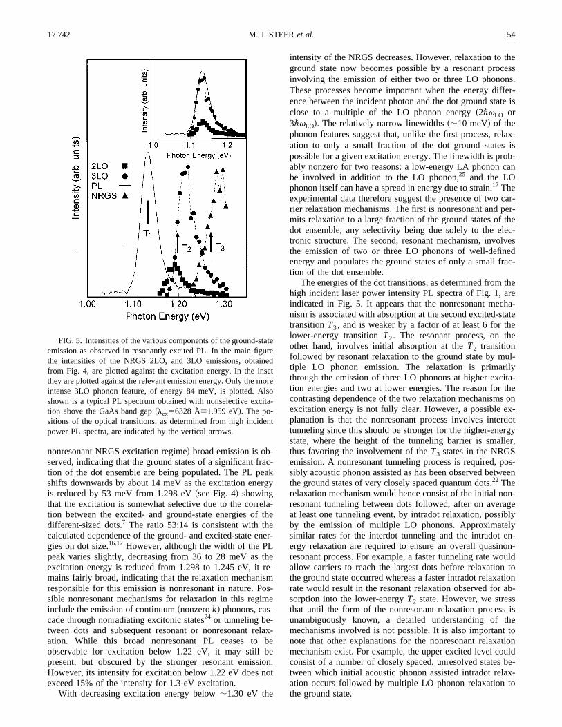
In the main part of Fig. 5 the intensities of the NRGS athe 2LO and 3LO phonon features, as observed in PL,plotted against the incident photon energy. A typical Pspectrum obtained with excitation at 1.959 eV, aboveGaAs band gap, is also shown for comparison. In the inthe intensities of the phonon features are plotted against trespective emission energies. Except for intensity the phocurves plotted in the inset are essentially identical to theobtained with above GaAs band-gap excitation, showing tthe same distribution of luminescent states is probed by eprocess. In particular, this indicates that the strengths ofindividual 2LO and 3LO multiple-phonon resonant relaation features are determined by the density of final~ground!radiative states.
The PL spectra of Fig. 4 and the data plotted in the mpart of Fig. 5 suggest that carriers can relax to the groustate of the dots by two distinct mechanisms, which we reto as ‘‘nonresonant’’ and ‘‘resonant,’’ respectively. The reltive importance of these two mechanisms depends uponexcitation energy. For high-energy excitation~*1.23 eV, the
FIG. 4. Selectively excited PL spectra obtained for a rangeexcitation energies. The dashed lines indicate a Gaussian fit tononresonant ground state~NRGS! emission. The dot-dashed lineindicate how the resonant features follow the excitation ene~note that as in PLE there are two features assigned to 3LO!.
-aearg
eltenLthresmoim
elbesioo
thecesss.iffer-te is
lax-isb-an
car-per-theec-lvesedrac-
thereha-tateee
ul-lyita-thes onx-rdotrgyler,
os-ween
on-ageiblylyn-on-ouldtotionab-sis
thetotionuldbe-
ax-to
tauneseolsita
en
17 742 54M. J. STEERet al.
nonresonant NRGS excitation regime! broad emission is observed, indicating that the ground states of a significant frtion of the dot ensemble are being populated. The PL pshifts downwards by about 14 meV as the excitation eneis reduced by 53 meV from 1.298 eV~see Fig. 4! showingthat the excitation is somewhat selective due to the corrtion between the excited- and ground-state energies ofdifferent-sized dots.7 The ratio 53:14 is consistent with thcalculated dependence of the ground- and excited-state egies on dot size.16,17However, although the width of the Ppeak varies slightly, decreasing from 36 to 28 meV asexcitation energy is reduced from 1.298 to 1.245 eV, itmains fairly broad, indicating that the relaxation mechaniresponsible for this emission is nonresonant in nature. Psible nonresonant mechanisms for relaxation in this reginclude the emission of continuum~nonzerok! phonons, cas-cade through nonradiating excitonic states24 or tunneling be-tween dots and subsequent resonant or nonresonant ration. While this broad nonresonant PL ceases toobservable for excitation below 1.22 eV, it may still bpresent, but obscured by the stronger resonant emisHowever, its intensity for excitation below 1.22 eV does nexceed 15% of the intensity for 1.3-eV excitation.
With decreasing excitation energy below;1.30 eV the
FIG. 5. Intensities of the various components of the ground-semission as observed in resonantly excited PL. In the main figthe intensities of the NRGS 2LO, and 3LO emissions, obtaifrom Fig. 4, are plotted against the excitation energy. In the inthey are plotted against the relevant emission energy. Only the mintense 3LO phonon feature, of energy 84 meV, is plotted. Ashown is a typical PL spectrum obtained with nonselective exction above the GaAs band gap~lex56328 Å[1.959 eV!. The po-sitions of the optical transitions, as determined from high incidpower PL spectra, are indicated by the vertical arrows.
c-ky
a-he
er-
e-
s-e
ax-e
n.t
intensity of the NRGS decreases. However, relaxation toground state now becomes possible by a resonant proinvolving the emission of either two or three LO phononThese processes become important when the energy dence between the incident photon and the dot ground staclose to a multiple of the LO phonon energy~2\vLO or3\vLO!. The relatively narrow linewidths~;10 meV! of thephonon features suggest that, unlike the first process, reation to only a small fraction of the dot ground statespossible for a given excitation energy. The linewidth is proably nonzero for two reasons: a low-energy LA phonon cbe involved in addition to the LO phonon,25 and the LOphonon itself can have a spread in energy due to strain.17 Theexperimental data therefore suggest the presence of tworier relaxation mechanisms. The first is nonresonant andmits relaxation to a large fraction of the ground states ofdot ensemble, any selectivity being due solely to the eltronic structure. The second, resonant mechanism, invothe emission of two or three LO phonons of well-definenergy and populates the ground states of only a small ftion of the dot ensemble.
The energies of the dot transitions, as determined fromhigh incident laser power intensity PL spectra of Fig. 1, aindicated in Fig. 5. It appears that the nonresonant mecnism is associated with absorption at the second excited-stransitionT3, and is weaker by a factor of at least 6 for thlower-energy transitionT2. The resonant process, on thother hand, involves initial absorption at theT2 transitionfollowed by resonant relaxation to the ground state by mtiple LO phonon emission. The relaxation is primarithrough the emission of three LO phonons at higher exction energies and two at lower energies. The reason forcontrasting dependence of the two relaxation mechanismexcitation energy is not fully clear. However, a possible eplanation is that the nonresonant process involves intetunneling since this should be stronger for the higher-enestate, where the height of the tunneling barrier is smalthus favoring the involvement of theT3 states in the NRGSemission. A nonresonant tunneling process is required, psibly acoustic phonon assisted as has been observed betthe ground states of very closely spaced quantum dots.22 Therelaxation mechanism would hence consist of the initial nresonant tunneling between dots followed, after on averat least one tunneling event, by intradot relaxation, possby the emission of multiple LO phonons. Approximatesimilar rates for the interdot tunneling and the intradot eergy relaxation are required to ensure an overall quasinresonant process. For example, a faster tunneling rate wallow carriers to reach the largest dots before relaxationthe ground state occurred whereas a faster intradot relaxarate would result in the resonant relaxation observed forsorption into the lower-energyT2 state. However, we stresthat until the form of the nonresonant relaxation processunambiguously known, a detailed understanding ofmechanisms involved is not possible. It is also importantnote that other explanations for the nonresonant relaxamechanism exist. For example, the upper excited level coconsist of a number of closely spaced, unresolved statestween which initial acoustic phonon assisted intradot relation occurs followed by multiple LO phonon relaxationthe ground state.
teredtreo-
t
s
igiteobgoeweieeogcasuriesethsn
nen
plav
euritc-n-itveth
ndoPdwslyLio
rfr,des
ot
,
u-toen-
velsed
east75
onttraa-volv-edpassro-
otsoftheittedtottedthe
54 17 743ELECTRONIC ENERGY LEVELS AND ENERGY . . .
An explanation for the selectivity of the resonant procehas been proposed by Heitzet al.16 Unlike quantum wellswhere there is only one variable dimension~the well width!,dots having different combinations of base length and hemay have the same ground-state energy but different excstate energies. As different ground-state energies are prby varying the PLE detection energy, those dots havinlevel spacing equal to an integer multiple of the LO phonenergy are the only ones that can relax to the ground statLO phonon emission. Hence the PLE spectra should shoconstant shift from the detection energy, as observed expmentally, the shift being determined by the phonon energrather than by the electronic level splitting. A further consquence of this mechanism is that carriers created in dhaving energy-level spacings not resonant with an intenumber of LO phonons are lost from the dot before theyrelax to the ground state. It has been suggested thatcarriers could transfer to deep levels in the GaAs barlayers.16 However, a more likely explanation is that thecarriers recombine radiatively from the excited states,resultant PL occurring at the excitation energy and conquently not being observable using the present experimetechnique.
Calculations suggest that the range of excited-state egies for a given ground state, resulting from dot size ashape fluctuations, is sufficient in the sample of Heitzet al.16
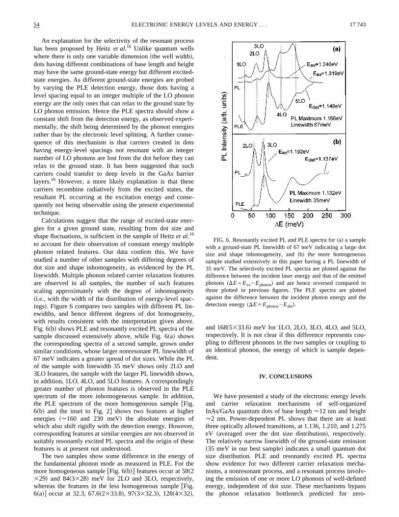
to account for their observation of constant energy multiphonon related features. Our data confirm this. We hstudied a number of other samples with differing degreesdot size and shape inhomogeneity, as evidenced by thelinewidth. Multiple phonon related carrier relaxation featurare observed in all samples, the number of such featscaling approximately with the degree of inhomogene~i.e., with the width of the distribution of energy-level spaings!. Figure 6 compares two samples with different PL liewidths, and hence different degrees of dot homogenewith results consistent with the interpretation given aboFig. 6~b! shows PLE and resonantly excited PL spectra ofsample discussed extensively above, while Fig. 6~a! showsthe corresponding spectra of a second sample, grown usimilar conditions, whose larger nonresonant PL linewidth67 meV indicates a greater spread of dot sizes. While theof the sample with linewidth 35 meV shows only 2LO an3LO features, the sample with the larger PL linewidth shoin addition, 1LO, 4LO, and 5LO features. A correspondinggreater number of phonon features is observed in the Pspectrum of the more inhomogeneous sample. In additthe PLE spectrum of the more homogeneous [email protected]~b! and the inset to Fig. 2# shows two features at higheenergies~'160 and 230 meV! the absolute energies owhich also shift rigidly with the detection energy. Howevecorresponding features at similar energies are not observesuitably resonantly excited PL spectra and the origin of thfeatures is at present not understood.
The two samples show some difference in the energythe fundamental phonon mode as measured in PLE. Formore homogeneous sample@Fig. 6~b!# features occur at 58~2329! and 84~3328! meV for 2LO and 3LO, respectivelywhereas the features in the less homogeneous [email protected]~a!# occur at 32.3, 67.6~2333.8!, 97~3332.3!, 128~4332!,
s
htd-edanbyari-s-tsernchr
ee-tal
r-d
eeofPLsesy
y,.e
erfL
,
En,
ine
fhe
and 168~5333.6! meV for 1LO, 2LO, 3LO, 4LO, and 5LO,respectively. It is not clear if this difference represents copling to different phonons in the two samples or couplingan identical phonon, the energy of which is sample depdent.
IV. CONCLUSIONS
We have presented a study of the electronic energy leand carrier relaxation mechanisms of self-organizInAs/GaAs quantum dots of base length'12 nm and height'2 nm. Power-dependent PL shows that there are at lthree optically allowed transitions, at 1.136, 1.210, and 1.2eV ~averaged over the dot size distribution!, respectively.The relatively narrow linewidth of the ground-state emissi~35 meV in our best sample! indicates a small quantum dosize distribution. PLE and resonantly excited PL specshow evidence for two different carrier relaxation mechnisms, a nonresonant process, and a resonant process ining the emission of one or more LO phonons of well-definenergy, independent of dot size. These mechanisms bythe phonon relaxation bottleneck predicted for ze
FIG. 6. Resonantly excited PL and PLE spectra for~a! a samplewith a ground-state PL linewidth of 67 meV indicating a large dsize and shape inhomogeneity, and~b! the more homogeneousample studied extensively in this paper having a PL linewidth35 meV. The selectively excited PL spectra are plotted againstdifference between the incident laser energy and that of the emphotons~DE5Eex2Ephoton! and are hence reversed comparedthose plotted in previous figures. The PLE spectra are ploagainst the difference between the incident photon energy anddetection energy~DE5Ephoton2Edet!.
thioef-o
thou
R.thencil
ndofe
ni
si
, H
,
ff
.
ei
ys
ys
Pun
i,
.
or-yst.
P.
..
ff,
s.
.
W.
17 744 54M. J. STEERet al.
dimensional systems. They differ in their dependence onexcitation energy, the former being dominant in relaxatfrom the higher~1.275 eV! excited state, the latter from thlower ~1.210 eV! state. By studying samples exhibiting diferent degrees of dot size and shape inhomogeneities wetain evidence supporting the recent proposal16 that the reso-nant relaxation mechanism is a consequence ofdistribution of energy-level separations in an inhomogeneensemble of dots.
*Also at Department of Electronic and Electrical Engineering, Uversity of Sheffield, Sheffield, S1 3JD, UK.
†Electronic address: [email protected]‡Present address: Cavendish Laboratory, Department of PhyUniversity of Cambridge, Cambridge, CB3 OHE, UK.
§Permanent address: Physics Department, Dartmouth Collegenover, NH 03755-3528.
1Y. Arakawa and A. Yariv, IEEE J. Quantum Electron.QE-22,1887 ~1986!.
2J. M. Moison, F. Houzay, F. Barthe, L. Leprince, E. Andre´, andO. Vatel, Appl. Phys. Lett.64, 196 ~1994!.
3J.-Y. Marzin, J. M. Ge´rard, A. Izrael, D. Barrier, and G. BastardPhys. Rev. Lett.73, 716 ~1994!.
4S. Fafard, R. Leon, D. Leonard, J. L. Merz, and P. M. PetroPhys. Rev. B50, 8086~1994!.
5M. Grundmann, J. Christen, N. N. Ledentsov, J. Bo¨hrer, D. Bim-berg, S. S. Ruvimov, P. Werner, U. Richter, U. Go¨sele, J. Hey-denreich, Y. M. Ustinov, A. Yu. Egorov, A. E. Zhukov, P. SKop’ev, and Zh. I. Alferov, Phys. Rev. Lett.74, 4043~1995!.
6S. Anand, N. Carlsson, M-E. Pistol, L. Samuelson, and W. Sert, Appl. Phys. Lett.67, 3016~1995!.
7S. Fafard, D. Leonard, J. L. Merz, and P. M. Petroff, Appl. PhLett. 65, 1388~1994!.
8D. Leonard, K. Pond, and P. M. Petroff, Phys. Rev. B50, 11 687~1994!.
9H. Benistry, C. M. Sottomayor-Torres, and C. Weisbuch, PhRev. B44, 10 945~1991!.
10T. H. Gfroerer, M. D. Sturge, K. Kash, J.A. Yater, A. S. Plaut,S. D. Lin, L. T. Florez, J. P. Harbison, S. R. Das, and L. LebrPhys. Rev. B53, 16 474~1996!.
11U. Bockelmann and T. Egeler, Phys. Rev. B46, 15 574~1992!.
en
b-
es
ACKNOWLEDGMENTS
We wish to acknowledge very useful discussions withHeitz and M. Grundmann, and the financial support ofEngineering and Physical Sciences Research Cou~EPSRC! U.K. One of us~M.D.S.! was supported in part bythe Faculty Research Fund of Dartmouth College, awishes to thank the Physics Department of the UniversitySheffield for their hospitality. D.J.M. would like to thank thEPSRC for financial support.
-
cs,
a-
,
f-
.
.
.,
12C. R. Kagan, C. B. Murray, M. Nirmal, and M. G. BawendPhys. Rev. Lett.76, 1517~1996!.
13A. G. Cullis, R. Murray, M. Hopkinson, M. J. Steer, and C. RWhitehouse~unpublished!.
14P. A. Claxton, J. S. Roberts, J. P. R. David, C. M. SotomayTorres, M. S. Skolnick, P. R. Tapster, and K. J. Nash, J. CrGrowth81, 288 ~1987!.
15G. Wang, S. Fafard, D. Leonard, J. E. Bowers, J. L. Merz, andM. Petroff, Appl. Phys. Lett.64, 2815~1994!.
16R. Heitz, M. Grundmann, N. N. Ledentsov, L. Eckey, M. Veit, DBimberg, V. M. Ustinov, A. Yu. Egorov, P. S. Kop’ev, and ZhI. Alferov, Appl. Phys. Lett.68, 361 ~1996!.
17M. Grundmann, O. Stier, and D. Bimberg, Phys. Rev. B52,11 969~1995!.
18S. Fafard, R. Leon, D. Leonard, J. L. Merz, and P. M. PetroPhys. Rev. B52, 5752~1995!.
19M. Grundmann,Advances in Solid State Physics~Vieweg, Braun-schweig, 1995!, Vol. 35.
20J-Y. Marzin and G. Bastard, Solid State Commun.92, 437~1994!.
21G. Medeiros-Ribeiro, D. Leonard, and P. M. Petroff, Appl. PhyLett. 66, 1767~1995!.
22A. Tackeuchi, Y. Nakata, S. Muto, Y. Sugiyama, T. Usuki, YNishikawa, N. Yokoyama, and O. Wada, Jpn. J. Appl. Phys.34,L1439 ~1995!.
23J. Hegarty, M. D. Sturge, C. Weisbuch, A. C. Gossard, andWiegmann, Phys. Rev. Lett.49, 930 ~1982!.
24U. Bockelmann, Phys. Rev. B48, 17 637~1993!.25T. Inoshita and H. Sakaki, Optoelectron. Devices Technol.8, 539
~1993!.
Related Documents