Electronic devices based upon Germanium nano-crystals with durability to strong neutron irradiation Itamar Baron 1 , Shai Levy 1 , Avraham Chelly 2 , Zeev Zalevsky 2 , Ofer Limon 2 , Shaobo Dun 3 , Tiecheng Lu 3 and Issai Shlimak 1 1 Jack and Pearl Resnick Institute of Advanced Technology, Physics Dept. Bar-Ilan Univ., Ramat-Gan, Israel 2 School of Engineering, Bar-Ilan Univ., Ramat-Gan, Israel 3 Physics Dept., Sichuan University, Chengdu, PR China ABSTRACT In this paper we present the preliminary experimental characterization of electronic devices based upon Germanium nano-crystals (nc-Ge) embedded in thick SiO 2 films grown on a Si substrate. The samples were prepared using Ge ion implantation followed by thermal annealing. Typical diameter of the nc-Ge is shown to be in the range of 4- 10nm. Gold (Au) contacts were deposited on the top of the oxide surface allowing measurements of the electronic properties. We present preliminary experimental results of electronic properties of the nc-Ge based devices including current-voltage (I-V) and capacitance-voltage (C-V) curves of the nano-devices while illuminated by white light and an external laser at a wavelength of 532nm for various levels of intensity. The characterization curves were also obtained at different temperatures. The proposed technology of devices based on nc-Ge was proven to be insensitive to high doses of irradiation by neutrons in a research nuclear reactor, which suggests that these nc-Ge devices can be used under extreme working conditions such as strong cosmic radiation appearing in outer space. Key words: Electronic devices, nano crystals, neutron irradiation. 1. INTRODUCTION Nanocrystals of Germanium (nc-Ge) embedded into an insulating SiO 2 matrix have been recently investigated as a new material for novel electronic devices [1-2]. The dominant fabrication process is ion implantation followed by a thermal annealing procedure [3-6]. The embedded nc-Ge are characterized by visible photoluminescense (PL) and are sensitive to external illumination making them a candidate for electro-optical devices [2]. In addition, one of the possible applications of such devices is in the field of nonvolatile memory structures due to the hysteresis of their capacitance-voltage characteristics [3-4, 6-15]. In this paper we experimentally characterize and demonstrate the use of nc-Ge based devices as electrical and photo activated devices. In our measurements we present the hysteresis property of the device which may be used for memory applications. We test the variation in electrical properties of the device, such as current-voltage (I-V) or capacitance-voltage (C-V), to temperature and external illumination. An important feature of the investigated material is its high durability to strong neutron and gamma radiation and accordingly to cosmic radiation in outer space. Therefore, these devices may be used as transistors, detectors and memory cells operating in an outer space environment or in other extreme conditions such as under strong neutron irradiation. 2. DEVICE DESCRIPTION The samples were fabricated using ion implantation of Ge + ions into amorphous SiO 2 films and subsequent thermal annealing. Ge + ions, with a dose of 1 × 10 17 ions/cm 2 , were accelerated to an energy of 150keV and were implanted onto the surface of 640 nm thick amorphous SiO 2 films initially grown on the surface of a < 100 > oriented single crystal Si substrate. This type of samples was labeled as ’as-implanted’ samples. The samples were subsequently Invited Paper Nanophotonics and Macrophotonics for Space Environments II, edited by Edward W. Taylor, David A. Cardimona, Proc. of SPIE Vol. 7095, 709502, (2008) · 0277-786X/08/$18 · doi: 10.1117/12.795667 Proc. of SPIE Vol. 7095 709502-1 2008 SPIE Digital Library -- Subscriber Archive Copy

Welcome message from author
This document is posted to help you gain knowledge. Please leave a comment to let me know what you think about it! Share it to your friends and learn new things together.
Transcript
Electronic devices based upon Germanium nano-crystals with durability to strong neutron irradiation
Itamar Baron1, Shai Levy1, Avraham Chelly2, Zeev Zalevsky2, Ofer Limon2, Shaobo Dun3,
Tiecheng Lu3 and Issai Shlimak1
1 Jack and Pearl Resnick Institute of Advanced Technology, Physics Dept. Bar-Ilan Univ., Ramat-Gan, Israel
2 School of Engineering, Bar-Ilan Univ., Ramat-Gan, Israel 3 Physics Dept., Sichuan University, Chengdu, PR China
ABSTRACT In this paper we present the preliminary experimental characterization of electronic devices based upon Germanium nano-crystals (nc-Ge) embedded in thick SiO2 films grown on a Si substrate. The samples were prepared using Ge ion implantation followed by thermal annealing. Typical diameter of the nc-Ge is shown to be in the range of 4-10nm. Gold (Au) contacts were deposited on the top of the oxide surface allowing measurements of the electronic properties.
We present preliminary experimental results of electronic properties of the nc-Ge based devices including current-voltage (I-V) and capacitance-voltage (C-V) curves of the nano-devices while illuminated by white light and an external laser at a wavelength of 532nm for various levels of intensity. The characterization curves were also obtained at different temperatures.
The proposed technology of devices based on nc-Ge was proven to be insensitive to high doses of irradiation by neutrons in a research nuclear reactor, which suggests that these nc-Ge devices can be used under extreme working conditions such as strong cosmic radiation appearing in outer space. Key words: Electronic devices, nano crystals, neutron irradiation.
1. INTRODUCTION Nanocrystals of Germanium (nc-Ge) embedded into an insulating SiO2 matrix have been recently investigated as a new material for novel electronic devices [1-2]. The dominant fabrication process is ion implantation followed by a thermal annealing procedure [3-6]. The embedded nc-Ge are characterized by visible photoluminescense (PL) and are sensitive to external illumination making them a candidate for electro-optical devices [2]. In addition, one of the possible applications of such devices is in the field of nonvolatile memory structures due to the hysteresis of their capacitance-voltage characteristics [3-4, 6-15].
In this paper we experimentally characterize and demonstrate the use of nc-Ge based devices as electrical and photo activated devices. In our measurements we present the hysteresis property of the device which may be used for memory applications. We test the variation in electrical properties of the device, such as current-voltage (I-V) or capacitance-voltage (C-V), to temperature and external illumination. An important feature of the investigated material is its high durability to strong neutron and gamma radiation and accordingly to cosmic radiation in outer space. Therefore, these devices may be used as transistors, detectors and memory cells operating in an outer space environment or in other extreme conditions such as under strong neutron irradiation.
2. DEVICE DESCRIPTION The samples were fabricated using ion implantation of Ge+ ions into amorphous SiO2 films and subsequent thermal annealing. Ge+ ions, with a dose of 1 × 10¹⁷ ions/cm2, were accelerated to an energy of 150keV and were implanted onto the surface of 640 nm thick amorphous SiO2 films initially grown on the surface of a < 100 > oriented single crystal Si substrate. This type of samples was labeled as ’as-implanted’ samples. The samples were subsequently
Invited Paper
Nanophotonics and Macrophotonics for Space Environments II, edited by Edward W. Taylor, David A. Cardimona, Proc. of SPIE Vol. 7095, 709502, (2008) · 0277-786X/08/$18 · doi: 10.1117/12.795667
Proc. of SPIE Vol. 7095 709502-12008 SPIE Digital Library -- Subscriber Archive Copy
uIJJ
uc (
ywoLbpon2 2!OS
Yn COU19
P100 > oL.GuGq 2!tLAI ! flIJ
I .6x1 08
-20 -10 10
Voltage(V)
20
-1 .Oxl 0
_/_ 0 20-2.Oxl 0 ____________________________ _________________________
Voltage(V)
annealed at a temperature of 8000C and labeled as ’as-prepared’ samples. The details of the fabrication and annealing conditions were published earlier in Ref. [5].
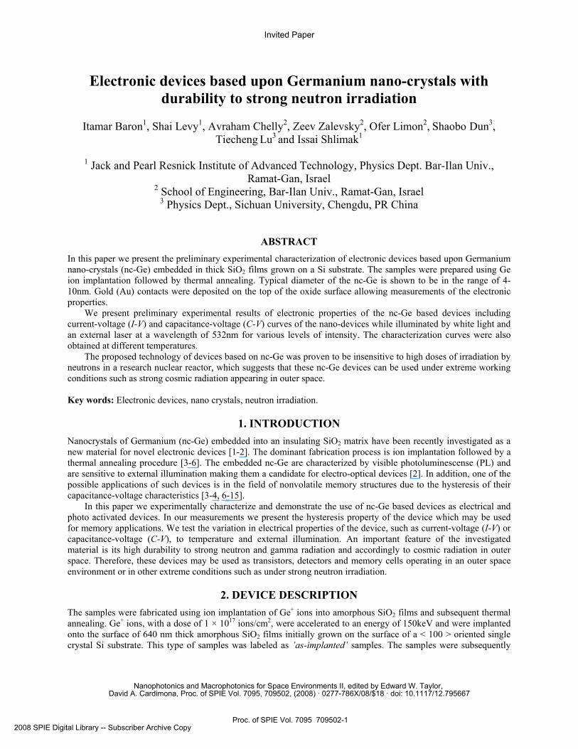
The nc-Ge formed in the 'as prepared' samples, were of spherical shape with a diameter range of 4-10 nm. Fig. 1(a) shows a schematic view of the 'as prepared' sample, Fig. 1(b) shows an HR-TEM image of nc-Ge.
(a). (b).
Fig. 1. (a). A schematic general view of the 'as prepared' sample. (b). HR-TEM images of an 'as prepared' sample, inset is the HR-TEM image of a Ge nanocrystal [5].
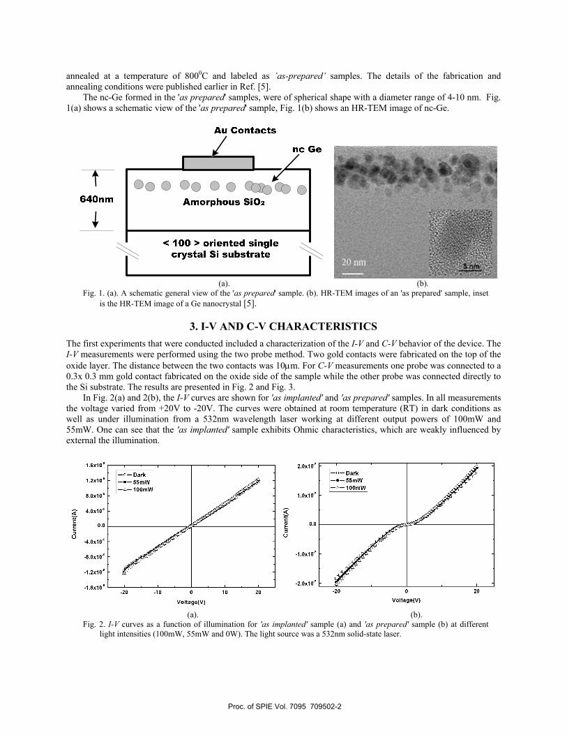
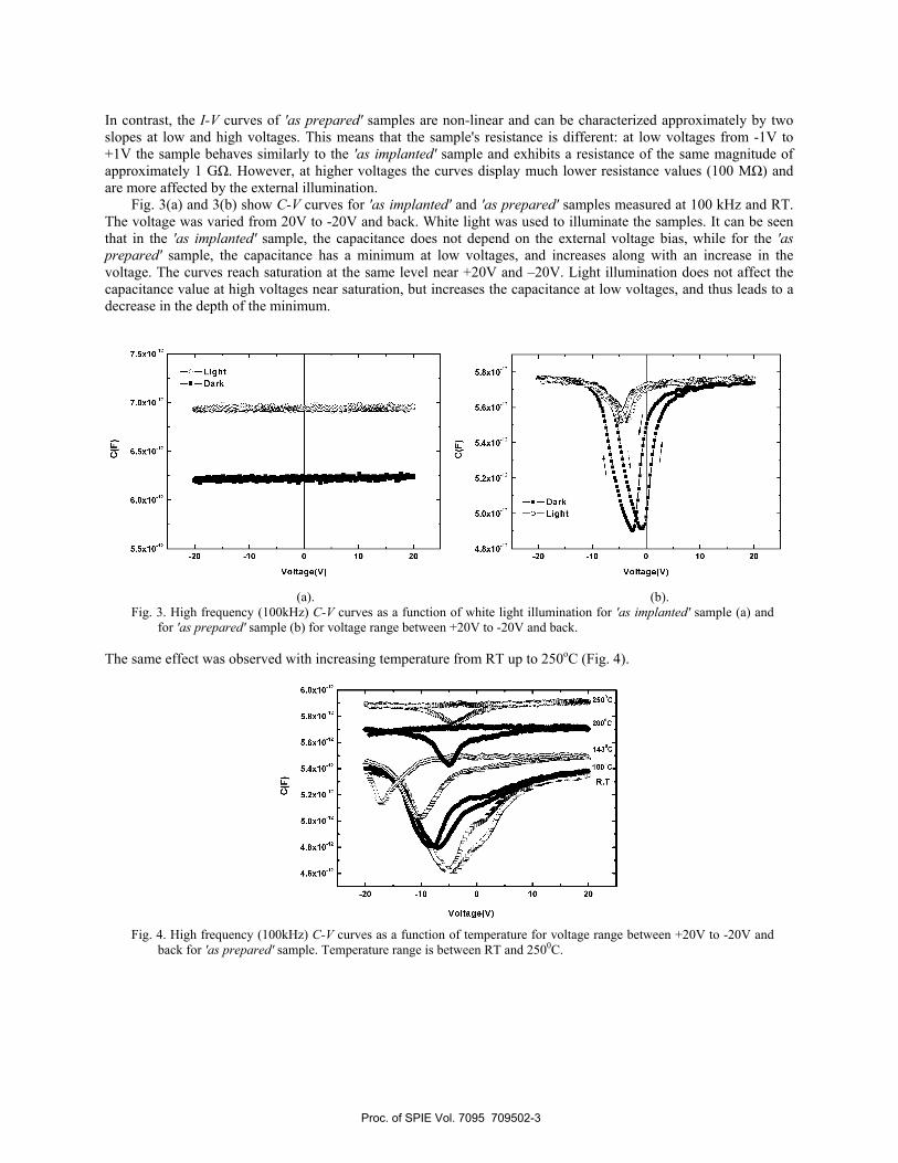
3. I-V AND C-V CHARACTERISTICS The first experiments that were conducted included a characterization of the I-V and C-V behavior of the device. The I-V measurements were performed using the two probe method. Two gold contacts were fabricated on the top of the oxide layer. The distance between the two contacts was 10µm. For C-V measurements one probe was connected to a 0.3x 0.3 mm gold contact fabricated on the oxide side of the sample while the other probe was connected directly to the Si substrate. The results are presented in Fig. 2 and Fig. 3.
In Fig. 2(a) and 2(b), the I-V curves are shown for 'as implanted' and 'as prepared' samples. In all measurements the voltage varied from +20V to -20V. The curves were obtained at room temperature (RT) in dark conditions as well as under illumination from a 532nm wavelength laser working at different output powers of 100mW and 55mW. One can see that the 'as implanted' sample exhibits Ohmic characteristics, which are weakly influenced by external the illumination.
(a). (b).
Fig. 2. I-V curves as a function of illumination for 'as implanted' sample (a) and 'as prepared' sample (b) at different light intensities (100mW, 55mW and 0W). The light source was a 532nm solid-state laser.
Proc. of SPIE Vol. 7095 709502-2
T.5x1 011 = __________________________ = I I
7.Oxl 012
U-6.5x10
6.Oxl 012
—0— Light—.— DarkS
—
-20 -10
Voltage(V)
10 20
Voltage(V)
Voltage(V)
In contrast, the I-V curves of 'as prepared' samples are non-linear and can be characterized approximately by two slopes at low and high voltages. This means that the sample's resistance is different: at low voltages from -1V to +1V the sample behaves similarly to the 'as implanted' sample and exhibits a resistance of the same magnitude of approximately 1 GΩ. However, at higher voltages the curves display much lower resistance values (100 MΩ) and are more affected by the external illumination.
Fig. 3(a) and 3(b) show C-V curves for 'as implanted' and 'as prepared' samples measured at 100 kHz and RT. The voltage was varied from 20V to -20V and back. White light was used to illuminate the samples. It can be seen that in the 'as implanted' sample, the capacitance does not depend on the external voltage bias, while for the 'as prepared' sample, the capacitance has a minimum at low voltages, and increases along with an increase in the voltage. The curves reach saturation at the same level near +20V and –20V. Light illumination does not affect the capacitance value at high voltages near saturation, but increases the capacitance at low voltages, and thus leads to a decrease in the depth of the minimum.
(a). (b).
Fig. 3. High frequency (100kHz) C-V curves as a function of white light illumination for 'as implanted' sample (a) and for 'as prepared' sample (b) for voltage range between +20V to -20V and back.
The same effect was observed with increasing temperature from RT up to 250oC (Fig. 4).
Fig. 4. High frequency (100kHz) C-V curves as a function of temperature for voltage range between +20V to -20V and
back for 'as prepared' sample. Temperature range is between RT and 2500C.
Proc. of SPIE Vol. 7095 709502-3
Ge nanocrystals
Conduction bandsIISi02
electrons •MU n-Sielectrode __________
11111 IValence bands
100I 640nm
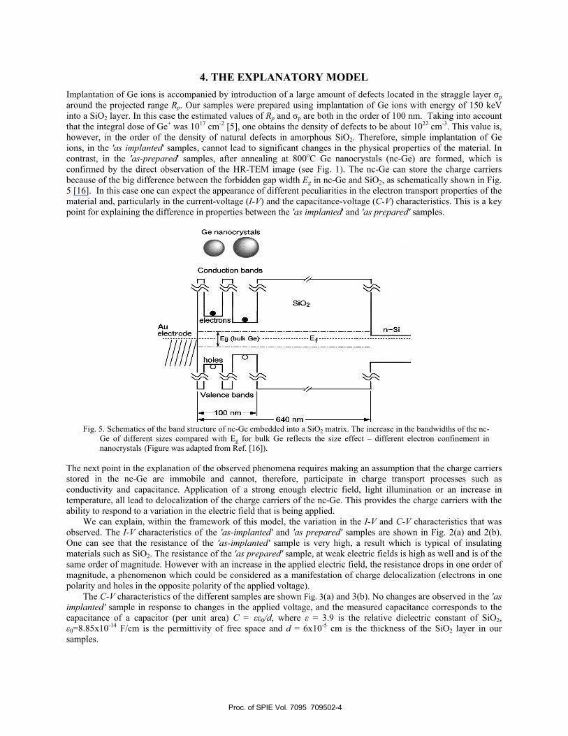
4. THE EXPLANATORY MODEL Implantation of Ge ions is accompanied by introduction of a large amount of defects located in the straggle layer σp around the projected range Rp. Our samples were prepared using implantation of Ge ions with energy of 150 keV into a SiO2 layer. In this case the estimated values of Rp and σp are both in the order of 100 nm. Taking into account that the integral dose of Ge+ was 1017 cm-2 [5], one obtains the density of defects to be about 1022 cm-3. This value is, however, in the order of the density of natural defects in amorphous SiO2. Therefore, simple implantation of Ge ions, in the 'as implanted' samples, cannot lead to significant changes in the physical properties of the material. In contrast, in the 'as-prepared' samples, after annealing at 800oC Ge nanocrystals (nc-Ge) are formed, which is confirmed by the direct observation of the HR-TEM image (see Fig. 1). The nc-Ge can store the charge carriers because of the big difference between the forbidden gap width Eg in nc-Ge and SiO2, as schematically shown in Fig. 5 [16]. In this case one can expect the appearance of different peculiarities in the electron transport properties of the material and, particularly in the current-voltage (I-V) and the capacitance-voltage (C-V) characteristics. This is a key point for explaining the difference in properties between the 'as implanted' and 'as prepared' samples.
Fig. 5. Schematics of the band structure of nc-Ge embedded into a SiO2 matrix. The increase in the bandwidths of the nc-
Ge of different sizes compared with Eg for bulk Ge reflects the size effect – different electron confinement in nanocrystals (Figure was adapted from Ref. [16]).
The next point in the explanation of the observed phenomena requires making an assumption that the charge carriers stored in the nc-Ge are immobile and cannot, therefore, participate in charge transport processes such as conductivity and capacitance. Application of a strong enough electric field, light illumination or an increase in temperature, all lead to delocalization of the charge carriers of the nc-Ge. This provides the charge carriers with the ability to respond to a variation in the electric field that is being applied.
We can explain, within the framework of this model, the variation in the I-V and C-V characteristics that was observed. The I-V characteristics of the 'as-implanted' and 'as prepared' samples are shown in Fig. 2(a) and 2(b). One can see that the resistance of the 'as-implanted' sample is very high, a result which is typical of insulating materials such as SiO2. The resistance of the 'as prepared' sample, at weak electric fields is high as well and is of the same order of magnitude. However with an increase in the applied electric field, the resistance drops in one order of magnitude, a phenomenon which could be considered as a manifestation of charge delocalization (electrons in one polarity and holes in the opposite polarity of the applied voltage).
The C-V characteristics of the different samples are shown Fig. 3(a) and 3(b). No changes are observed in the 'as implanted' sample in response to changes in the applied voltage, and the measured capacitance corresponds to the capacitance of a capacitor (per unit area) C = εε0/d, where ε = 3.9 is the relative dielectric constant of SiO2, ε0=8.85x10⁻¹⁴ F/cm is the permittivity of free space and d = 6x10⁻⁵ cm is the thickness of the SiO2 layer in our samples.
Proc. of SPIE Vol. 7095 709502-4
IA'
LII
/fAA ••.
/.
—.—As Prepared— — As Irradiated
560 570 580 590 600 610 620
Wavelength [nm]
In contrast, in the 'as prepared' sample the capacitance increases with applied voltage and around V = ± 20V saturates at a value which is approximately 15% larger than the capacitance at low voltages. This can be explained by the fact that the immobile carriers which are located at an average depth of 40-60 nm below the surface become mobile at high voltages. The mobile charges can cause a screening of the applied electric field and reduce the effective thickness of the insulating layer of the capacitor (about 15%), which in turn leads to a corresponding increase in the capacitance value. The C-V characteristics, therefore, exhibit a minimum at low voltages.
The clearly observed hysteresis indicates that the processes in which charge carriers become mobile and frozen are non-equilibrium processes and therefore non-symmetric, at least not at room temperature and in the time interval of the conducted measurements. This fact is encouraging for an application of nc-Ge based devices as memory cells.
Illuminating the sample by light quanta and increasing the temperature both lead to delocalization of the stored charges even at zero voltage, a fact that explains the increase in the minima of the C-V curves as it is seen in Fig. 3(b) and Fig. 4.
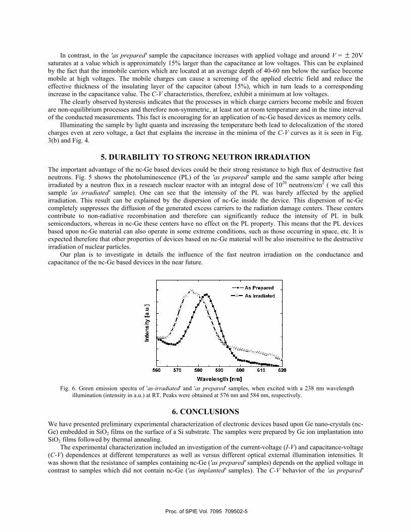
5. DURABILITY TO STRONG NEUTRON IRRADIATION The important advantage of the nc-Ge based devices could be their strong resistance to high flux of destructive fast neutrons. Fig. 5 shows the photoluminescence (PL) of the 'as prepared' sample and the same sample after being irradiated by a neutron flux in a research nuclear reactor with an integral dose of 1020 neutrons/cm2 ( we call this sample 'as irradiated' sample). One can see that the intensity of the PL was barely affected by the applied irradiation. This result can be explained by the dispersion of nc-Ge inside the device. This dispersion of nc-Ge completely suppresses the diffusion of the generated excess carriers to the radiation damage centers. These centers contribute to non-radiative recombination and therefore can significantly reduce the intensity of PL in bulk semiconductors, whereas in nc-Ge these centers have no effect on the PL property. This means that the PL devices based upon nc-Ge material can also operate in some extreme conditions, such as those occurring in space, etc. It is expected therefore that other properties of devices based on nc-Ge material will be also insensitive to the destructive irradiation of nuclear particles.
Our plan is to investigate in details the influence of the fast neutron irradiation on the conductance and capacitance of the nc-Ge based devices in the near future.
Fig. 6. Green emission spectra of 'as-irradiated' and 'as prepared' samples, when excited with a 238 nm wavelength
illumination (intensity in a.u.) at RT. Peaks were obtained at 576 nm and 584 nm, respectively.
6. CONCLUSIONS We have presented preliminary experimental characterization of electronic devices based upon Ge nano-crystals (nc-Ge) embedded in SiO2 films on the surface of a Si substrate. The samples were prepared by Ge ion implantation into SiO2 films followed by thermal annealing.
The experimental characterization included an investigation of the current-voltage (I-V) and capacitance-voltage (C-V) dependences at different temperatures as well as versus different optical external illumination intensities. It was shown that the resistance of samples containing nc-Ge ('as prepared' samples) depends on the applied voltage in contrast to samples which did not contain nc-Ge ('as implanted' samples). The C-V behavior of the 'as prepared'
Proc. of SPIE Vol. 7095 709502-5
samples had a U-shape (with minimum capacitance at low voltages), exhibited a hysteresis which presents memory properties and is strongly affected by external illumination. These characteristics open the way for the creation of light-controlled nano-size memory cells.
An explanatory model is presented which provides justification for all the observed peculiarities in the I-V and the C-V dependences assuming that nc-Ge are the storing centers of the charge carriers (electrons and holes) which can be delocalized by applying external electric field, light illumination or increase in temperature.
In addition, it is shown that the photoluminescence (PL) properties of the nc-Ge based material are insensitive to the high doses of irradiation by nuclear reactor neutrons. This allows suggesting these devices for extreme working conditions such as strong cosmic radiation.
ACKNOWLEDGEMENTS Issai Shlimak thanks the Erick and Sheila Samson Chair of Semiconductor Technology for financial support.
REFERENCES [1] P.W. Li, W. M. Liao, D. M. T. Kuo, S. W. Lin, P. S. Chen, S. C. Lu and M.-J. Tsai, "Fabrication of a
germanium quantum-dot single-electron transistor with large Coulomb-blockade oscillations at room temperature," Appl. Phys. Lett. 85, 1532-1534 (2004).
[2] J.-M. Shieh, Y.-F. Lai, W.-X. Ni, H.-C. Kuo, C.-Y. Fang, J. Y. Huang and C.-L. Pan, "Enhanced photoresponse of a metal-oxide-semiconductor photodetector with silicon nanocrystals embedded in the oxide layer," Appl. Phys. Lett. 90, 051105.1-051105.3 (2007).
[3] C.-H. Tu and T.-C. Chang, "Formation of germanium nanocrystals embedded in silicon-oxygen-nitride layer," Appl. Phys. Lett. 89, 052112 (2006).
[4] S. Duguay, J. J. Grob, A. Slaoui, Y. Le Gall and M Amann-Liess, "Structural and electrical properties of Ge nanocrystals embedded in SiO2 by ion implantation and annealing," J. Appl. Phys. 97, 104330_1-5 (2005).
[5] Y. Hu, T. Lu, S. Dun, Q. Hu, N. Huang, S. Zhang, B. Tang, J. Dai, L. Resnick, I. Shlimak, S.Zhu, Q. Wei and L. Wang, "The Raman spectroscopy of neutron transmutation doping isotope 74Germanium nanocrystals embedded in SiO2 matrix," Solid State Communications 141, 514-518 (2007).
[6] C. J. Park, H. Y. Cho, S. Kim, S.-H. Choi, R. G. Elliman, J. H. Han, C. Kim, H. N. Hwang and C. C. Hwang, "Annealing temperature dependence of capacitance-voltage characteristics in Ge-nanocrystal-based nonvolatile memory structures," J. Appl. Phys. 99, 36101 (2006).
[7] T. H. Ng, W. K. Chim, and W. K. Choi, "Conductance-voltage measurements on germanium nanocrystal memory structures and effect of gate electric field coupling," Appl. Phys. Lett. 88, 113112 (2006).
[8] A. Kanjilal, J. Lundsgaard Hansen, P.Gaiduk, A. Nylandsted Larsen, N. Cherkashin, A. Claverie, P.Normard, E. Kapalanakis, D. Skarlatos, D. Tsoukalas, "Structural and electrical properties of silicon dioxide layers with embedded germanium nanocrystals grown by molecular beam epitaxy," Appl. Phys. Lett. 82, 1212-1214 (2003).
[9] S. Das, K. Das, R. K. Singha, A. Dhar and S. K. Ray, "Improved charge injection characteristics of Ge nanocrystals embedded in hafnium oxide for floating gate devices," Appl. Phys. Lett. 91, 233118 (2007).
[10] J. H. Chen, Y. Q. Wang, W. J. Yoo, Y.-C. Yeo, G. Samudra, D. S. Chan, A. Y. Du and D.-L. Kwong, "Nonvolatile flash memory device using Ge nanocrystals embedded in HfAlO high-/spl kappa/tunneling and control oxides: Device fabrication and electrical performance," IEEE Transactions on Electron Devices 51, 1840–1848 (2004).
[11] B. H. Koh, E. W. H. Kan, W. K. Chim, W. K. Choi, D. A. Antoniadis and E. A. Fitzgerald, "Traps in germanium nanocrystal memory and effect on charge retention: Modeling and experimental measurements," J. Appl. Phys. 97, 124305 (2005).
[12] C.-H. Tu, T.-C. Chang, P.-T. Liu, H.-C. Liu, S. M. Sze and C.-Y. Chang, "Improved memory window for Ge nanocrystals embedded in SiON layer," Appl. Phys. Lett. 89, 162105 (2006).
[13] O. González-Varona, B. Garrido, S. Cheylan, A. Pérez-Rodríguez, A. Cuadras and J. R. Morante, "Control of tunnel oxide thickness in Si-nanocrystal array memories obtained by ion implantation and its impact in writing speed and volatility," Appl. Phys. Lett. 82, 2151-2153 (2003).
[14] Q. Wan, N. L. Zhang, W. L. Liu, C. L. Lin and T. H. Wang, "Memory and negative photoconductivity effects of Ge nanocrystals embedded in ZrO2Al2O3 gate dielectrics," Appl. Phys. Lett. 83, 138-140 (2003).
[15] M. Kanoun, A. Souifi, T. Baron and F. Mazen, "Electrical study of Ge-nanocrystal-based metal-oxide-semiconductor structures for p-type nonvolatile memory applications," Appl. Phys. Lett. 84, 5079-5081 (2004).
Proc. of SPIE Vol. 7095 709502-6
[16] M. Fujii, O. Mamezaki, S. Hayashi and K. Yamamoto, "Current Transport Properties of SiO2 Films Containing Ge Nanocrystals," J. Appl. Phys. 83, 1507-1512 (1998).
Proc. of SPIE Vol. 7095 709502-7
Related Documents


