W I T H M A T L A B ® C O M P U T I N G Orchard Publications www.orchardpublications.com Steven T. Karris Electronic Devices and Amplifier Circuits Second Edition

Welcome message from author
This document is posted to help you gain knowledge. Please leave a comment to let me know what you think about it! Share it to your friends and learn new things together.
Transcript
WITH MATLAB® COMPU
TIN
G
Orchard Publicationswww.orchardpublications.com
Steven T. Karris
Electronic Devicesand Amplifier Circuits
Second Edition

Orchard PublicationsVisit us on the Internet
www.orchardpublications.comor email us: [email protected]
Steven T. Karris is the founder and president of Orchard Publications, has undergraduate andgraduate degrees in electrical engineering, and is a registered professional engineer in California and Florida. He has more than 35 years of professional engineering experience and more than 30 years of teaching experience as an adjunct professor, most recently at UC Berkeley, California. His area of interest is in The MathWorks, Inc.™ products and the publication of MATLAB® and Simulink® based texts.
This text includes the following chapters and appendices:• Basic Electronic Concepts and Signals • Introduction to Semiconductor Electronics - Diodes• Bipolar Junction Transistors • Field Effect Transistors and PNPN Devices • Operational Amplifiers• Integrated Circuits • Pulse Circuits and Waveforms Generators • Frequency Characteristics ofSingle-Stage and Cascaded Amplifiers • Tuned Amplifiers • Sinusoidal Oscillators • Introduction toMATLAB® • Introduction to Simulink® • PID Controllers • Compensated Attenuators • TheSubstitution, Reduction, and Miller’s Theorems
Each chapter contains numerous practical applications supplemented with detailed instructionsfor using MATLAB to plot the characteristics of non-linear devices and to obtain quick solutions.
Electronic Devicesand Amplifier Circuits
with MATLAB® ComputingSecond Edition
$70.00 U.S.A.
ISBN-10: 1-9934404-114-44
ISBN-13: 978-11-9934404-114-00
Students and working professionals willfind Electronic Devices and Amplifier Circuitswith MATLAB® Computing, Second Edition,to be a concise and easy-to-learn text. Itprovides complete, clear, and detailedexplanations of the state-of-the-art elec-tronic devices and integrated circuits. Alltopics are illustrated with many real-worldexamples.
Electronic Devicesand Amplifier Circuits
with MATLAB®Computing
Second EditionSteven T. Karris
Orchard Publicationswww.orchardpublications.com

Electronic Devices and Amplifier Circuits with MATLAB®Computing, Second Edition
Copyright ” 2008 Orchard Publications. All rights reserved. Printed in the United States of America. No part of thispublication may be reproduced or distributed in any form or by any means, or stored in a data base or retrieval system,without the prior written permission of the publisher.
Direct all inquiries to Orchard Publications, [email protected]
Product and corporate names are trademarks or registered trademarks of The MathWorks, Inc. They are used only foridentification and explanation, without intent to infringe.
Library of Congress Cataloging-in-Publication Data
Library of Congress Control Number (LCCN) 2008934432
TXu1−254-969
ISBN-13: 978−1−934404−14−0
ISBN-10: 1−934404−14−4
Disclaimer
The author has made every effort to make this text as complete and accurate as possible, but no warranty is implied.The author and publisher shall have neither liability nor responsibility to any person or entity with respect to any lossor damages arising from the information contained in this text.
Preface
This text is an undergraduate level textbook presenting a thorough discussion of state−of−the artelectronic devices. It is self−contained; it begins with an introduction to solid state semiconductordevices. The prerequisites for this text are first year calculus and physics, and a two−semestercourse in circuit analysis including the fundamental theorems and the Laplace transformation. Noprevious knowledge of MATLAB®is required; the material in Appendix A and the inexpensiveMATLAB Student Version is all the reader needs to get going. Our discussions are based on a PCwith Windows XP platforms but if you have another platform such as Macintosh, please refer tothe appropriate sections of the MATLAB’s User Guide which also contains instructions forinstallation. Additional information including purchasing may be obtained from The MathWorks,Inc., 3 Apple Hill Drive, Natick, MA 01760-2098. Phone: 508 647−7000, Fax: 508 647−7001, e−mail: [email protected] and web site http://www.mathworks.com.This text can also be usedwithout MATLAB.
This is our fourth electrical and computer engineering-based text with MATLAB applications.My associates, contributors, and I have a mission to produce substance and yet inexpensive textsfor the average reader. Our first three texts* are very popular with students and workingprofessionals seeking to enhance their knowledge and prepare for the professional engineeringexamination.
The author and contributors make no claim to originality of content or of treatment, but havetaken care to present definitions, statements of physical laws, theorems, and problems.
Chapter 1 is an introduction to the nature of small signals used in electronic devices, amplifiers,definitions of decibels, bandwidth, poles and zeros, stability, transfer functions, and Bode plots.Chapter 2 is an introduction to solid state electronics beginning with simple explanations ofelectron and hole movement. This chapter provides a thorough discussion on the junction diodeand its volt-ampere characteristics. In most cases, the non-linear characteristics are plotted withsimple MATLAB scripts. The discussion concludes with diode applications, the Zener, Schottky,tunnel, and varactor diodes, and optoelectronics devices. Chapters 3 and 4 are devoted to bipolarjunction transistors and FETs respectively, and many examples with detailed solutions areprovided. Chapter 5 is a long chapter on op amps. Many op amp circuits are presented and theirapplications are well illustrated.
The highlight of this text is Chapter 6 on integrated devices used in logic circuits. The internalconstruction and operation of the TTL, NMOS, PMOS, CMOS, ECL, and the biCMOS families
* These are Circuit Analysis I, ISBN 978−0−9709511−2−0, Circuit Analysis II, ISBN 978−0−9709511−5−1, and Signals and Systems, 978−1−934404−11−9.

of those devices are fully discussed. Moreover, the interpretation of the most importantparameters listed in the manufacturers data sheets are explained in detail. Chapter 7 is anintroduction to pulse circuits and waveform generators. There, we discuss the 555 Timer, theastable, monostable, and bistable multivibrators, and the Schmitt trigger.
Chapter 8 discusses to the frequency characteristic of single-stage and cascade amplifiers, andChapter 9 is devoted to tuned amplifiers. Sinusoidal oscillators are introduced in Chapter 10.
This is the second edition of this title, and includes several Simulink models. Also, two newappendices have been added. Appendix A, is an introduction to MATLAB. Appendix B is anintroduction to Simulink, Appendix C is an introduction to Proportional-Integral-Derivative(PID) controllers, Appendix D describes uncompensated and compensated networks, andAppendix D discusses the substitution, reduction, and Miller’s theorems.
The author wishes to express his gratitude to the staff of The MathWorks™, the developers ofMATLAB® and Simulink® for the encouragement and unlimited support they have provided mewith during the production of this text.
A companion to this text, Digital Circuit Analysis and Design with Simulink® Modeling andIntroduction to CPLDs and FPGAs, ISBN 978−1−934404−05−8 is recommended as a companion.This text is devoted strictly on Boolean logic, combinational and sequential circuits asinterconnected logic gates and flip−flops, an introduction to static and dynamic memory devices.and other related topics.
Although every effort was made to correct possible typographical errors and erroneous referencesto figures and tables, some may have been overlooked. Our experience is that the best proofreaderis the reader. Accordingly, the author will appreciate it very much if any such errors are brought tohis attention so that corrections can be made for the next edition. We will be grateful to readerswho direct these to our attention at [email protected]. Thank you.
Orchard PublicationsFremont, California 94538−4741United States of [email protected]
Electronic Devices and Amplifier Circuits with MATLAB Computing, Second Edition iCopyright © Orchard Publications
Table of Contents1 Basic Electronic Concepts and Signals
1.1 Signals and Signal Classifications ......................................................................... 1−11.2 Amplifiers .............................................................................................................. 1−31.3 Decibels ................................................................................................................. 1−41.4 Bandwidth and Frequency Response .................................................................... 1−51.5 Bode Plots............................................................................................................. 1−81.6 Transfer Function ................................................................................................. 1−91.7 Poles and Zeros.................................................................................................... 1−111.8 Stability ............................................................................................................... 1−121.9 Voltage Amplifier Equivalent Circuit ................................................................. 1−171.10 Current Amplifier Equivalent Circuit................................................................. 1−191.11 Summary ............................................................................................................. 1−211.12 Exercises .............................................................................................................. 1−241.13 Solutions to End−of−Chapter Exercises.............................................................. 1−26
MATLAB ComputingPages 1−7, 1−14, 1−15, 1−19, 1−27, 1−28, 1−31
Simulink ModelingPages 1−34, 1−35
2 Introduction to Semiconductor Electronics − Diodes
2.1 Electrons and Holes ............................................................................................... 2−12.2 Junction Diode ...................................................................................................... 2−42.3 Graphical Analysis of Circuits with Non−Linear Devices ..................................... 2−92.4 Piecewise Linear Approximations....................................................................... 2−132.5 Low Frequency AC Circuits with Junction Diodes ............................................ 2−152.6 Junction Diode Applications in AC Circuits...................................................... 2−192.7 Peak Rectifier Circuits ........................................................................................ 2−302.8 Clipper Circuits ................................................................................................... 2−322.9 DC Restorer Circuits........................................................................................... 2−352.10 Voltage Doubler Circuits .................................................................................... 2−362.11 Diode Applications in Amplitude Modulation (AM) Detection Circuits ......... 2−372.12 Diode Applications in Frequency Modulation (FM) Detection Circuits........... 2−372.13 Zener Diodes ....................................................................................................... 2−382.14 Schottky Diode ................................................................................................... 2−452.15 Tunnel Diode ...................................................................................................... 2−452.16 Varactor .............................................................................................................. 2−48
ii Electronic Devices and Amplifier Circuits with MATLAB Computing, Second EditionCopyright © Orchard Publications
2.17 Optoelectronic Devices .......................................................................................2−492.18 Summary..............................................................................................................2−522.19 Exercises ..............................................................................................................2−562.20 Solutions to End−of−Chapter Exercises ..............................................................2−61
MATLAB ComputingPages 2−27, 2−28, 2−29, 2−61, 2−70
Simulink ModelingPages 2−19, 2−22, 2−25, 2−30
3 Bipolar Junction Transistors
3.1 Introduction ....................................................................................................... 3−13.2 NPN Transistor Operation ................................................................................ 3−33.3 Bipolar Junction Transistor as an Amplifier ...................................................... 3−3
3.3.1 Equivalent Circuit Models − NPN Transistors........................................ 3−63.3.2 Equivalent Circuit Models − PNP Transistors ........................................ 3−73.3.3 Effect of Temperature on the − Characteristics...................... 3−103.3.4 Collector Output Resistance − Early Voltage ....................................... 3−11
3.4 Transistor Amplifier Circuit Biasing ................................................................ 3−183.5 Fixed Bias ......................................................................................................... 3−213.6 Self−Bias ........................................................................................................... 3−253.7 Amplifier Classes and Operation ..................................................................... 3−28
3.7.1 Class A Amplifier Operation................................................................. 3−313.7.2 Class B Amplifier Operation ................................................................. 3−343.7.3 Class AB Amplifier Operation .............................................................. 3−353.7.4 Class C Amplifier Operation................................................................. 3−37
3.8 Graphical Analysis ........................................................................................... 3−383.9 Power Relations in the Basic Transistor Amplifier .......................................... 3−423.10 Piecewise−Linear Analysis of the Transistor Amplifier ................................... 3−443.11 Incremental Linear Models .............................................................................. 3−493.12 Transconductance............................................................................................ 3−543.13 High−Frequency Models for Transistors .......................................................... 3−553.14 The Darlington Connection ............................................................................ 3−603.15 Transistor Networks......................................................................................... 3−61
3.15.1 h−Equivalent Circuit for the Common−Base Transistor..................... 3−613.15.2 T−Equivalent Circuit for the Common−Base Transistor .................... 3−643.15.3 h−Equivalent Circuit for the Common−Emitter Transistor ................ 3−653.15.4 T−Equivalent Circuit for the Common−Emitter Transistor................ 3−703.15.5 h−Equivalent Circuit for the Common−Collector Transistor ............. 3−713.15.6 T−Equivalent Circuit for the Common−Collector Transistor............. 3−76
iC vBE–
Electronic Devices and Amplifier Circuits with MATLAB Computing, Second Edition iiiCopyright © Orchard Publications
3.16 Transistor Cutoff and Saturation Regions..................................................... 3−773.16.1 Cutoff Region ....................................................................................3−783.16.2 Active Region....................................................................................3−783.16.3 Saturation Region .............................................................................3−78
3.17 The Ebers−Moll Transistor Model................................................................. 3−813.18 Schottky Diode Clamp...................................................................................3−853.19 Transistor Specifications................................................................................3−853.20 Summary ........................................................................................................3−873.21 Exercises.........................................................................................................3−913.22 Solutions to End−of−Chapter Exercises ........................................................3−97
MATLAB ComputingPages 3−13, 3−39, 3−113
4 Field Effect Transistors and PNPN Devices
4.1 Junction Field Effect Transistor (JFET)............................................................. 4−14.2 Metal Oxide Semiconductor Field Effect Transistor (MOSFET) ..................... 4−6
4.2.1 N−Channel MOSFET in the Enhancement Mode................................... 4−84.2.2 N−Channel MOSFET in the Depletion Mode ...................................... 4−124.2.3 P−Channel MOSFET in the Enhancement Mode ................................. 4−144.2.4 P−Channel MOSFET in the Depletion Mode ....................................... 4−174.2.5 Voltage Gain ......................................................................................... 4−17
4.3 Complementary MOS (CMOS)....................................................................... 4−194.3.1 CMOS Common−Source Amplifier ..................................................... 4−204.3.2 CMOS Common−Gate Amplifier......................................................... 4−204.3.3 CMOS Common−Drain (Source Follower) Amplifier ......................... 4−20
4.4 Metal Semiconductor FET (MESFET)............................................................ 4−214.5 Unijunction Transistor ..................................................................................... 4−224.6 Diac.................................................................................................................. 4−234.7 Silicon Controlled Rectifier (SCR).................................................................. 4−24
4.7.1 SCR as an Electronic Switch ................................................................ 4−274.7.2 SCR in the Generation of Sawtooth Waveforms .................................. 4−28
4.8 Triac ............................................................................................................... 4−374.9 Shockley Diode.............................................................................................. 4−384.10 Other PNPN Devices...................................................................................... 4−404.11 The Future of Transistors ............................................................................... 4−414.12 Summary........................................................................................................ 4−424.13 Exercises ........................................................................................................ 4−454.14 Solutions to End−of−Chapter Exercises ........................................................ 4−47
MATLAB ComputingPages 4−5, 4−10

iv Electronic Devices and Amplifier Circuits with MATLAB Computing, Second EditionCopyright © Orchard Publications
5 Operational Amplifiers
5.1 Operational Amplifier.......................................................................................5−15.2 An Overview of the Op Amp ...........................................................................5−15.3 Op Amp in the Inverting Mode........................................................................5−25.4 Op Amp in the Non−Inverting Mode ..............................................................5−55.5 Active Filters.....................................................................................................5−85.6 Analysis of Op Amp Circuits ..........................................................................5−115.7 Input and Output Resistances ........................................................................5−225.8 Op Amp Open Loop Gain ..............................................................................5−255.9 Op Amp Closed Loop Gain ............................................................................5−265.10 Transresistance Amplifier ...............................................................................5−295.11 Closed Loop Transfer Function ......................................................................5−305.12 Op Amp Integrator .........................................................................................5−315.13 Op Amp Differentiator ...................................................................................5−355.14 Summing and Averaging Op Amp Circuits ....................................................5−375.15 Differential Input Op Amp..............................................................................5−395.16 Instrumentation Amplifiers .............................................................................5−425.17 Offset Nulling ..................................................................................................5−445.18 External Frequency Compensation .................................................................5−455.19 Slew Rate .........................................................................................................5−455.20 Circuits with Op Amps and Non-Linear Devices ...........................................5−465.21 Comparators ....................................................................................................5−505.22 Wien Bridge Oscillator ....................................................................................5−505.23 Digital−to−Analog Converters ........................................................................5−525.24 Analog−to−Digital Converters ........................................................................5−56
5.24.1 Flash Analog−to−Digital Converter ....................................................5−575.24.2 Successive Approximation Analog−to−Digital Converter..................5−585.24.3 Dual−Slope Analog−to−Digital Converter..........................................5−59
5.25 Quantization, Quantization Error, Accuracy, and Resolution.......................5−615.26 Op Amps in Analog Computers .....................................................................5−635.27 Summary .........................................................................................................5−675.28 Exercises..........................................................................................................5−715.29 Solutions to End−of−Chapter Exercises .........................................................5−78
MATLAB ComputingPages 5−80, 5−89
6 Integrated Circuits6.1 Basic Logic Gates.............................................................................................. 6−16.2 Positive and Negative Logic ..............................................................................6−1
Electronic Devices and Amplifier Circuits with MATLAB Computing, Second Edition vCopyright © Orchard Publications
6.3 Inverter ............................................................................................................. 6−26.4 AND Gate......................................................................................................... 6−66.5 OR Gate............................................................................................................ 6−86.6 NAND Gate ..................................................................................................... 6−96.7 NOR Gate....................................................................................................... 6−146.8 Exclusive OR (XOR) and Exclusive NOR (XNOR) Gates ........................... 6−156.9 Fan-In, Fan-Out, TTL Unit Load, Sourcing Current, and Sinking Current . 6−176.10 Data Sheets ..................................................................................................... 6−206.11 Emitter Coupled Logic (ECL)......................................................................... 6−246.12 NMOS Logic Gates......................................................................................... 6−28
6.12.1 NMOS Inverter................................................................................... 6−316.12.2 NMOS NAND Gate ........................................................................... 6−316.12.3 NMOS NOR Gate .............................................................................. 6−32
6.13 CMOS Logic Gates ........................................................................................ 6−326.13.1 CMOS Inverter ................................................................................... 6−336.13.2 CMOS NAND Gate ........................................................................... 6−346.13.3 The CMOS NOR Gate ....................................................................... 6−35
6.14 Buffers, Tri-State Devices, and Data Buses ................................................... 6−356.15 Present and Future Technologies................................................................... 6−396.16 Summary......................................................................................................... 6−436.17 Exercises ......................................................................................................... 6−466.18 Solutions to End−of−Chapter Exercises ......................................................... 6−49
7 Pulse Circuits and Waveform Generators
7.1 Astable (Free-Running) Multivibrators ........................................................... 7−17.2 555 Timer ......................................................................................................... 7−27.3 Astable Multivibrator with 555 Timer ............................................................. 7−37.4 Monostable Multivibrators ............................................................................. 7−147.5 Bistable Multivibrators (Flip−Flops)............................................................... 7−19
7.5.1 Fixed−Bias Flip-Flop............................................................................ 7−197.5.2 Self−Bias Flip−Flop .............................................................................. 7−227.5.3 Triggering Signals for Flip−Flops ......................................................... 7−287.5.4 Present Technology Bistable Multivibrators ....................................... 7−30
7.6 The Schmitt Trigger ....................................................................................... 7−307.7 Summary......................................................................................................... 7−337.8 Exercises ......................................................................................................... 7−347.9 Solutions to End−of−Chapter Exercises ......................................................... 7−37
MATLAB ComputingPages 7−11, 7−26, 7−38, 7−39

vi Electronic Devices and Amplifier Circuits with MATLAB Computing, Second EditionCopyright © Orchard Publications
8 Frequency Characteristics of Single−Stage and Cascaded Amplifiers
8.1 Properties of Signal Waveforms........................................................................8−18.2 The Transistor Amplifier at Low Frequencies..................................................8−58.3 The Transistor Amplifier at High Frequencies.................................................8−98.4 Combined Low- and High−Frequency Characteristics...................................8−148.5 Frequency Characteristics of Cascaded Amplifiers ........................................8−158.6 Overall Characteristics of Multistage Amplifiers ...........................................8−278.7 Amplification and Power Gain in Three or More Cascaded Amplifiers ........8−328.8 Summary .........................................................................................................8−348.9 Exercises..........................................................................................................8−368.10 Solutions to End−of−Chapter Exercises..........................................................8−39
MATLAB ComputingPages 8−9, 8−25, 8−45
9 Tuned Amplifiers
9.1 Introduction to Tuned Circuits..........................................................................9−19.2 Single-tuned Transistor Amplifier......................................................................9−89.3 Cascaded Tuned Amplifiers .............................................................................9−14
9.3.1 Synchronously Tuned Amplifiers ...........................................................9−149.3.2 Stagger−Tuned Amplifiers......................................................................9−189.3.3 Three or More Tuned Amplifiers Connected in Cascade......................9−27
9.4 Summary...........................................................................................................9−289.5 Exercises ...........................................................................................................9−309.6 Solutions to End−of−Chapter Exercises ...........................................................9−31
MATLAB ComputingPage 9−18
10 Sinusoidal Oscillators
10.1 Introduction to Oscillators ...........................................................................10−110.2 Sinusoidal Oscillators ...................................................................................10−110.3 RC Oscillator................................................................................................10−410.4 LC Oscillators ...............................................................................................10−510.5 The Armstrong Oscillator ............................................................................10−610.6 The Hartley Oscillator .................................................................................10−710.7 The Colpitts Oscillator.................................................................................10−710.8 Crystal Oscillators ........................................................................................10−810.9 The Pierce Oscillator..................................................................................10−10
Electronic Devices and Amplifier Circuits with MATLAB Computing, Second Edition viiCopyright © Orchard Publications
10.10 Summary .................................................................................................... 10−1210.11 Exercises ..................................................................................................... 10−1410.12 Solutions to End−of−Chapter Exercises..................................................... 10−15
A Introduction to MATLAB®
A.1 MATLAB® and Simulink®......................................................................... A−1A.2 Command Window....................................................................................... A−1A.3 Roots of Polynomials ..................................................................................... A−3A.4 Polynomial Construction from Known Roots............................................... A−4A.5 Evaluation of a Polynomial at Specified Values............................................ A−6A.6 Rational Polynomials..................................................................................... A−8A.7 Using MATLAB to Make Plots .................................................................. A−10A.8 Subplots....................................................................................................... A−18A.9 Multiplication, Division and Exponentiation ............................................. A−18A.10 Script and Function Files ............................................................................ A−26A.11 Display Formats........................................................................................... A−31
MATLAB ComputingPages A−3 through A−8, A−10, A−13, A−14, A−16, A−17,A−21, A−22, A−24, A−27
B Introduction to Simulink®
B.1 Simulink and its Relation to MATLAB..............................................................B−1B.2 Simulink Demos................................................................................................B−20
MATLAB ComputingPage B−4
Simulink ModelingPages B−7, B−12, B−14, B−18
C Proportional−Integral−Derivative (PID) Controller
C.1 Description and Components of a Typical PID................................................. C−1C.2 The Simulink PID Blocks .................................................................................. C−2
Simulink ModelingPages C−2, C−3
D Compensated Attenuators
D.1 Uncompensated Attenuator .............................................................................. D−1D.2 Compensated Attenuator .................................................................................. D−2

viii Electronic Devices and Amplifier Circuits with MATLAB Computing, Second EditionCopyright © Orchard Publications
E Substitution, Reduction, and Miller’s Theorems
E.1 The Substitution Theorem ..................................................................................E−1E.2 The Reduction Theorem .....................................................................................E−6E.3 Miller’s Theorem...............................................................................................E−10
References R−1
Index IN−1

Electronic Devices and Amplifier Circuits with MATLAB Computing, Second Edition 1−1Copyright © Orchard Publications
Chapter 1
Basic Electronic Concepts and Signals
lectronics may be defined as the science and technology of electronic devices and systems.Electronic devices are primarily non−linear devices such as diodes and transistors and ingeneral integrated circuits (ICs) in which small signals (voltages and currents) are applied to
them. Of course, electronic systems may include resistors, capacitors and inductors as well.Because resistors, capacitors and inductors existed long ago before the advent of semiconductordiodes and transistors, these devices are thought of as electrical devices and the systems that con-sist of these devices are generally said to be electrical rather than electronic systems. As we know,with today’s technology, ICs are becoming smaller and smaller and thus the modern IC technologyis referred to as microelectronics.
1.1 Signals and Signal ClassificationsA signal is any waveform that serves as a means of communication. It represents a fluctuating elec-tric quantity, such as voltage, current, electric or magnetic field strength, sound, image, or anymessage transmitted or received in telegraphy, telephony, radio, television, or radar. Figure 1.1shows a typical signal that varies with time where can be any physical quantity such asvoltage, current, temperature, pressure, and so on.
Figure 1.1. Typical waveform of a signal
We will now define the average value of a waveform.
Consider the waveform shown in Figure 1.2. The average value of in the interval is
(1.1)
E
f t( ) f t( )
f t( )
t
f t( ) a t b≤ ≤
f t( )ave ab Area
Period-----------------
f t( ) tda
b∫
b a–------------------------= =

Chapter 1 Basic Electronic Concepts and Signals
1−2 Electronic Devices and Amplifier Circuits with MATLAB Computing, Second EditionCopyright © Orchard Publications
Figure 1.2. Defining the average value of a typical waveform
A periodic time function satisfies the expression
(1.2)
for all time and for all integers . The constant is the period and it is the smallest value oftime which separates recurring values of the waveform.
An alternating waveform is any periodic time function whose average value over a period is zero.Of course, all sinusoids are alternating waveforms. Others are shown in Figure 1.3.
Figure 1.3. Examples of alternating waveforms
The effective (or RMS) value of a periodic current waveform denoted as is the current
that produces heat in a given resistor at the same average rate as a direct (constant) current, that is,
(1.3)
Also, in a periodic current waveform the instantaneous power is
(1.4)
and
(1.5)
f b( )f a( )f t( )
Area
Perioda b
t
f t( ) f t nT+( )=
t n T
t t t
TT T
i t( ) Ieff
RIdc
Average Power Pave RIeff2 RIdc
2= = =
i t( ) p t( )
p t( ) Ri 2 t( )=
Pave1T--- p t( ) td
0
T
∫ 1T--- Ri 2 td
0
T
∫ RT---- i 2 td
0
T
∫= = =

Electronic Devices and Amplifier Circuits with MATLAB Computing, Second Edition 1−3Copyright © Orchard Publications
Amplifiers
Equating (1.3) with (1.5) we obtain
or(1.6)
or(1.7)
where RMS stands for Root Mean Squared, that is, the effective value or value of a cur-rent is computed as the square root of the mean (average) of the square of the current.
Warning 1: In general, . implies that the current must first be squared
and the average of the squared value is to be computed. On the other hand, implies thatthe average value of the current must first be found and then the average must be squared.
Warning 2: In general, . If and for exam-
ple, and , it follows that also. However,
In introductory electrical engineering books it is shown* that if the peak (maximum) value of acurrent of a sinusoidal waveform is , then
(1.8)
and we must remember that (1.8) applies to sinusoidal values only.
1.2 AmplifiersAn amplifier is an electronic circuit which increases the magnitude of the input signal. The symbolof a typical amplifier is a triangle as shown in Figure 1.4.
Figure 1.4. Symbol for electronic amplifier
* Please refer to Circuit Analysis I with MATLAB Applications, ISBN 978−0−9709511−2−0.
RIeff2 R
T---- i2 td
0
T
∫=
Ieff2 1
T--- i2 td
0
T
∫=
IRMS Ieff1T--- i2 td
0
T
∫ Ave i2( )= = =
Ieff IRMS
Ave i2( ) iave( )2≠ Ave i2( ) i
iave( )2
Pave Vave Iave⋅≠ v t( ) Vp ωtcos= i t( ) Ip ωt θ+( )cos=
Vave 0= Iave 0= Pave 0=
Pave1T--- p td
0
T∫
1T--- vi td
0
T∫ 0≠= =
Ip
IRMS Ip 2⁄ 0.707Ip= =
voutvin
Chapter 1 Basic Electronic Concepts and Signals
1−4 Electronic Devices and Amplifier Circuits with MATLAB Computing, Second EditionCopyright © Orchard Publications
An electronic (or electric) circuit which produces an output that is smaller than the input iscalled an attenuator. A resistive voltage divider* is a typical attenuator.
An amplifier can be classified as a voltage, current or power amplifier. The gain of an amplifier isthe ratio of the output to the input. Thus, for a voltage amplifier
or
The current gain and power gain are defined similarly.
1.3 DecibelsThe ratio of any two values of the same quantity (power, voltage or current) can be expressed indecibels (dB). For instance, we say that an amplifier has power gain, or a transmissionline has a power loss of (or gain ). If the gain (or loss) is , the output is equal tothe input. We should remember that a negative voltage or current gain or indicates that
there is a phase difference between the input and the output waveforms. For instance, if anop amp has a gain of (dimensionless number), it means that the output is out−of−phase with the input. For this reason we use absolute values of power, voltage and current whenthese are expressed in terms to avoid misinterpretation of gain or loss.
By definition,
(1.9)
Therefore,
represents a power ratio of
represents a power ratio of
It is useful to remember that
represents a power ratio of
represents a power ratio of
represents a power ratio of
* Please refer to Circuit Analysis I with MATLAB Applications, ISBN 978−0−9709511−2−0.
Voltage Gain Output VoltageInput Voltage
-----------------------------------------=
Gv Vout Vin⁄=
Gi Gp
10 dB7 dB 7 dB– 0 dB
Gv Gi
180°100– 180°
dB
dB 10 PoutPin---------log=
10 dB 10
10n dB 10n
20 dB 100
30 dB 1 000,
60 dB 1 000 000, ,

Electronic Devices and Amplifier Circuits with MATLAB Computing, Second Edition 1−5Copyright © Orchard Publications
Bandwidth and Frequency Response
Also,
represents a power ratio of approximately
represents a power ratio of approximately
represents a power ratio of approximately
From these, we can estimate other values. For instance, which is equivalentto a power ratio of approximately . Likewise, and this isequivalent to a power ratio of approximately .
Since and , if we let the values for voltage andcurrent ratios become
(1.10)
and(1.11)
1.4 Bandwidth and Frequency ResponseLike electric filters, amplifiers exhibit a band of frequencies over which the output remains nearlyconstant. Consider, for example, the magnitude of the output voltage of an electric or elec-
tronic circuit as a function of radian frequency as shown in Figure 1.5.
As shown in Figure 1.5, the bandwidth is where and are the cutoff frequen-
cies. At these frequencies, and these two points are known as the 3−dB
down or half−power points . They derive their name from the fact that since power
, for and for or the power is , that is, it is“halved”.
Figure 1.5. Definition of bandwidth
1 dB 1.25
3 dB 2
7 dB 5
4 dB 3 dB 1 dB+=
2 1.25× 2.5= 27 dB 20 dB 7 dB+=
100 5× 500=
y x2log 2 xlog= = P V2 Z⁄ I2 Z⋅= = Z 1= dB
dBv 10 Vout
Vin----------
2log 20 Vout
Vin----------log= =
dBi 10 Iout
Iin-------
2log 20 Iout
Iin-------log= =
Vout
ω
BW ω2 ω1–= ω1 ω2
Vout 2 2⁄ 0.707= =
p v2 R⁄ i2 R⋅= = R 1= v i 2 2⁄ 0.707= = 1 2⁄
1
0.707
ωω1 ω2
Bandwidth
Vout

Chapter 1 Basic Electronic Concepts and Signals
1−6 Electronic Devices and Amplifier Circuits with MATLAB Computing, Second EditionCopyright © Orchard Publications
Alternately, we can define the bandwidth as the frequency band between half−power points. Werecall from the characteristics of electric filters, the low−pass and high−pass filters have only onecutoff frequency whereas band−pass and band−elimination (band−stop) filters have two. We maythink that low−pass and high−pass filters have also two cutoff frequencies where in the case ofthe low−pass filter the second cutoff frequency is at while in a high−pass filter it is at
.
We also recall also that the output of circuit is dependent upon the frequency when the input is asinusoidal voltage. In general form, the output voltage is expressed as
(1.12)
where is known as the magnitude response and is known as the phase response.These two responses together constitute the frequency response of a circuit.
Example 1.1
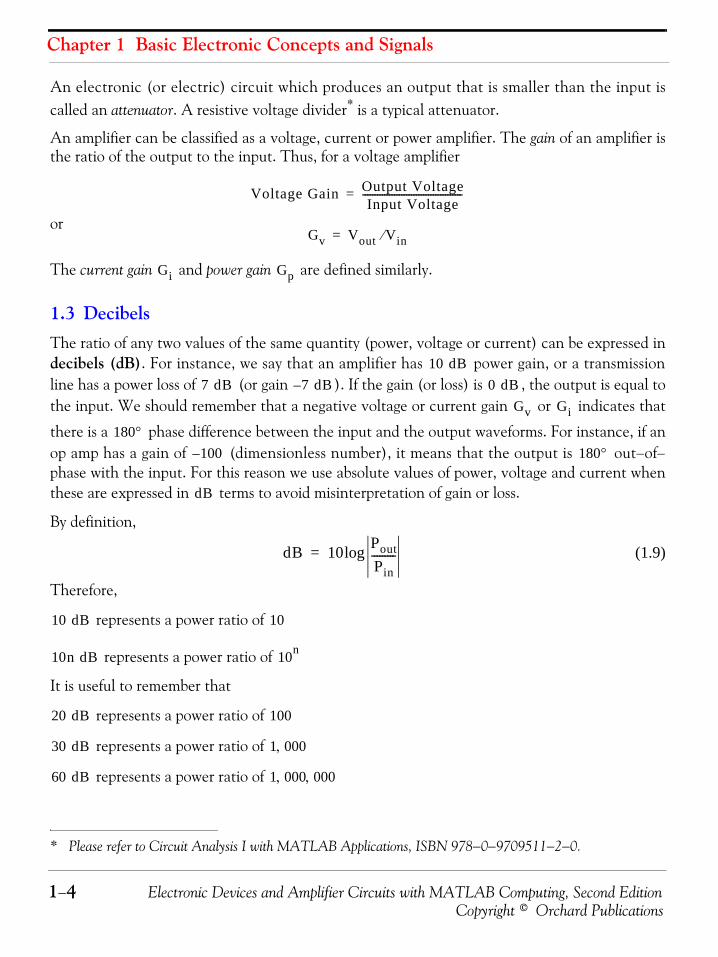
Derive and sketch the magnitude and phase responses of the low−pass filter shown in Figure1.6.
Figure 1.6. RC low−pass filterSolution:By application of the voltage division expression we obtain
(1.13)
or(1.14)
and thus the magnitude is(1.15)
and the phase angle (sometimes called argument and abbreviated as arg) is
ω 0=
ω ∞=
Vout ω( ) Vout ω( ) e jϕ ω( )=
Vout ω( ) e jϕ ω( )
RC
RCvin vout
Vout1 jωC⁄
R 1 jωC⁄+---------------------------Vin=
VoutVin----------- 1
1 jωRC+------------------------=
VoutVin----------- 1
1 ω2R2C2+ ωRC( )1–tan∠
--------------------------------------------------------------------- 1
1 ω2R2C2+--------------------------------- ωRC( )1–tan–∠= =
VoutVin----------- 1
1 ω2R2C2+
---------------------------------=

Electronic Devices and Amplifier Circuits with MATLAB Computing, Second Edition 1−7Copyright © Orchard Publications
Bandwidth and Frequency Response
(1.16)
To sketch the magnitude, we let assume the values , , and . Then,
as ,
for ,
and as ,
To sketch the phase response, we use (1.16). Then,
as ,
as ,
for ,
as ,
The magnitude and phase responses of the low−pass filter are shown in Figure 1.7.
Figure 1.7. Magnitude and phase responses for the low−pass filter of Figure 1.6
We can use MATLAB* to plot the magnitude and phase angle for this low-pass filter using rela-tion (1.13) expressed in MATLAB script below and plot the magnitude and phase angle in semi-log scale.
w=1:10:100000; RC=1; xf=1./(1+j.*w.*RC);...mag=20.*log10(abs(xf)); phase=angle(xf).*180./pi;... subplot(121); semilogx(w,mag); subplot(122); semilogx(w,phase)
* For an introduction to MATLAB, please refer to Appendix A
ϕVoutVin-----------
⎝ ⎠⎜ ⎟⎛ ⎞
arg ωRC( )1–tan–= =
ω 0 1 RC⁄ ∞
ω 0→ Vout Vin⁄ 1≅
ω 1 RC⁄= Vout Vin⁄ 1 2( )⁄ 0.707= =
ω ∞→ Vout Vin⁄ 0≅
ω ∞–→ φ ∞–( )1–tan– 90°≅ ≅
ω 0→ φ 01–tan– 0≅ ≅
ω 1 RC⁄= φ 11–tan– 45–°≅ ≅
ω ∞→ φ ∞( )1–tan– 90°–≅ ≅
RC
0
−1/RC 1/RC
ϕ90°
−90°
ω
ω
Vout
Vin
1
0.707
1/RC
45°
−45°
Chapter 1 Basic Electronic Concepts and Signals
1−8 Electronic Devices and Amplifier Circuits with MATLAB Computing, Second EditionCopyright © Orchard Publications
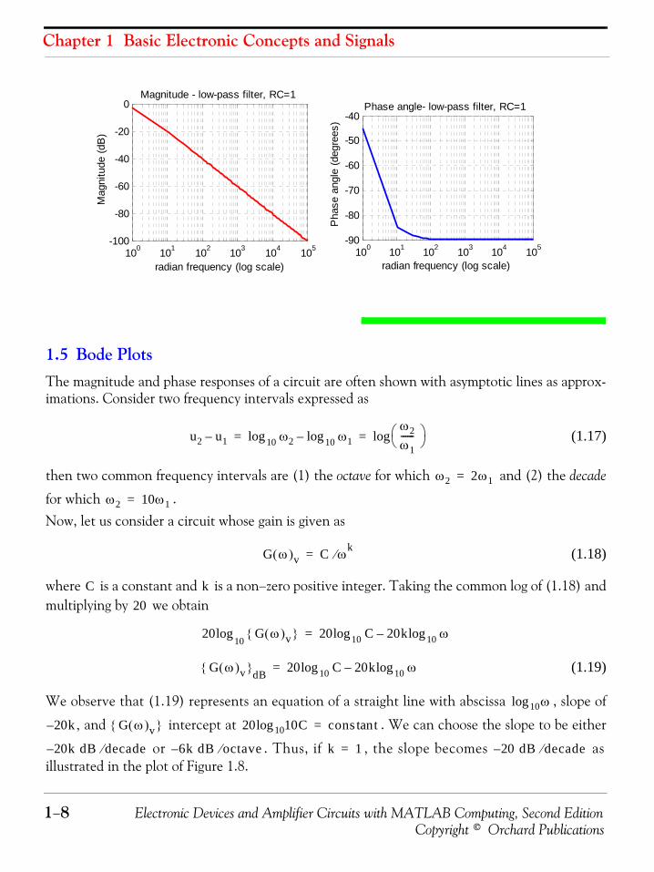
1.5 Bode PlotsThe magnitude and phase responses of a circuit are often shown with asymptotic lines as approx-imations. Consider two frequency intervals expressed as
(1.17)
then two common frequency intervals are (1) the octave for which and (2) the decade
for which .Now, let us consider a circuit whose gain is given as
(1.18)
where is a constant and is a non−zero positive integer. Taking the common log of (1.18) andmultiplying by we obtain
(1.19)
We observe that (1.19) represents an equation of a straight line with abscissa , slope of
, and intercept at . We can choose the slope to be either
or . Thus, if , the slope becomes asillustrated in the plot of Figure 1.8.
100
101
102
103
104
105
-100
-80
-60
-40
-20
0
radian frequency (log scale)
Mag
nitu
de (
dB)
Magnitude - low-pass filter, RC=1
100
101
102
103
104
105
-90
-80
-70
-60
-50
-40
radian frequency (log scale)
Pha
se a
ngle
(de
gree
s)
Phase angle- low-pass filter, RC=1
u2 u1– ω10 2log ω10 1log–ω2ω1------⎝ ⎠
⎛ ⎞log= =
ω2 2ω1=
ω2 10ω1=
G ω( )v C ωk⁄=
C k20
20 G ω( )v{ }10 log 20 C10 log 20k ω10 log–=
G ω( )v{ } dB 20 C10 log 20k ω10 log–=
ω10log
20k– G ω( )v{ } 20 1010 Clog cons ttan=
20k dB decade⁄– 6k dB octave⁄– k 1= 20 dB decade⁄–
Electronic Devices and Amplifier Circuits with MATLAB Computing, Second Edition 1−9Copyright © Orchard Publications
Transfer Function
Figure 1.8. Plot of relation (1.19) for
Then, any line parallel to this slope will represent a drop of . We observe also that ifthe exponent in (1.18) is changed to , the slope will be .
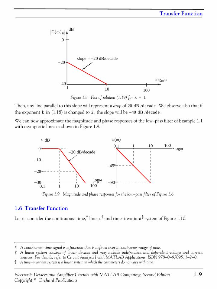
We can now approximate the magnitude and phase responses of the low−pass filter of Example 1.1with asymptotic lines as shown in Figure 1.9.
Figure 1.9. Magnitude and phase responses for the low−pass filter of Figure 1.6.
1.6 Transfer Function
Let us consider the continuous−time,* linear,† and time−invariant‡ system of Figure 1.10.
* A continuous−time signal is a function that is defined over a continuous range of time.† A linear system consists of linear devices and may include independent and dependent voltage and current
sources. For details, refer to Circuit Analysis I with MATLAB Applications, ISBN 978−0−9709511−2−0.‡ A time−invariant system is a linear system in which the parameters do not vary with time.
1−40
10 100
log10ω
−20
0
dB
slope = −20 dB/decade
G ω( )V
k 1=
20 dB decade⁄k 2 40 dB decade⁄–
0
−10
−20
−30
−45°
−90°0.1 1 10 100
−20 dB/decade
logω
logω0.1 1 10 100dB ϕ(ω)

Chapter 1 Basic Electronic Concepts and Signals
1−10 Electronic Devices and Amplifier Circuits with MATLAB Computing, Second EditionCopyright © Orchard Publications
Figure 1.10. Input−output block diagram for linear, time−invariant continuous−time system
We will assume that initially no energy is stored in the system. The input−output relationship canbe described by the differential equation of
(1.20)
For practically all electric networks, and the integer denotes the order of the system.
Taking the Laplace transform* of both sides of (1.20) we obtain
Solving for we obtain
where and are the numerator and denominator polynomials respectively.
The transfer function is defined as
(1.21)
Example 1.2
Derive the transfer function of the network in Figure 1.11.
* The Laplace transform and its applications to electric circuit analysis is discussed in detail in Circuit AnalysisII, ISBN 978−0−9709511−5−1.
invariant system
Continuous time,–linear, and time-
vin t( ) vout t( )
bmdm
dtm---------vout t( ) bm 1–
dm 1–
dtm 1–----------------vout t( ) bm 2–
dm 2–
dtm 2–----------------vout t( ) … b0vout t( ) =+ + + +
andn
dtn-------vin t( ) an 1–
dn 1–
dt n 1–---------------vin t( ) an 2–
dn 2–
dtn 2–---------------vin t( ) … a0vin t( )+ + + +
m n≥ m
bmsm bm 1– sm 1– bm 2– sm 2– … b0+ + + +( )Vout s( ) =
ansn an 1– sn 1– an 2– sn 2– … a0+ + + +( )Vin s( )
Vout s( )
Vout s( )ansn an 1– sn 1– an 2– sn 2– … a0+ + + +( )
bmsm bm 1– sm 1– bm 2– sm 2– … b0+ + + +( )----------------------------------------------------------------------------------------------------------------Vin s( ) N s( )
D s( )-----------Vin s( )= =
N s( ) D s( )
G s( )
G s( )Vout s( )
Vin s( )------------------ N s( )
D s( )-----------= =
G s( )

Electronic Devices and Amplifier Circuits with MATLAB Computing, Second Edition 1−11Copyright © Orchard Publications
Poles and Zeros
Figure 1.11. Network for Example 1.2
Solution:
The given circuit is in the .* The transfer function exists only in the †
and thus we redraw the circuit in the as shown in Figure 1.12.
Figure 1.12. Circuit of Example 1.2 in the
For relatively simple circuits such as that of Figure 1.12, we can readily obtain the transfer func-tion with application of the voltage division expression. Thus, parallel combination of the capaci-tor and resistor yields
and by application of the voltage division expression
or
1.7 Poles and ZerosLet
(1.22)
* For brevity, we will denote the time domain as † Henceforth, the complex frequency, i.e., , will be referred to as the .
L
0.5 H+
− −
+
vin t( )−+
C 1 F R 1 Ω vout t( )
t domain– G s( ) s domain–
t domain–
s σ jω+= s domain–
s domain–
+
− −
+
−
+Vin s( )
0.5s
1 s⁄ 1 Vout s( )
s domain–
1 s⁄ 1×1 s 1+⁄------------------ 1
s 1+-----------=
Vout s( ) 1 s 1+( )⁄0.5s 1 s 1+( )⁄+----------------------------------------Vin s( )=
G s( )Vout s( )
Vin s( )------------------ 2
s2 s 2+ +-----------------------= =
F s( ) N s( )D s( )-----------=
Chapter 1 Basic Electronic Concepts and Signals
1−12 Electronic Devices and Amplifier Circuits with MATLAB Computing, Second EditionCopyright © Orchard Publications
where and are polynomials and thus (1.22) can be expressed as
(1.23)
The coefficients and for are real numbers and, for the present discus-
sion, we have assumed that the highest power of is less than the highest power of , i.e.,. In this case, is a proper rational function. If , is an improper rational function.
It is very convenient to make the coefficient of in (12.2) unity; to do this, we rewrite it as
(1.24)
The roots of the numerator are called the zeros of , and are found by letting in(1.24). The roots of the denominator are called the poles* of and are found by letting
. However, in most engineering applications we are interested in the nature of thepoles.
1.8 StabilityIn general, a system is said to be stable if a finite input produces a finite output. We can predictthe stability of a system from its impulse response† . In terms of the impulse response,
1. A system is stable if the impulse response goes to zero after some time as shown in Figure1.13.
2. A system is marginally stable if the impulse response reaches a certain non−zero value butnever goes to zero as shown in Figure 1.14.
3. A system is unstable if the impulse response reaches infinity after a certain time as shownin Figure 1.15.
* The zeros and poles can be distinct (different from one another), complex conjugates, repeated, of a combina-tion of these. For details refer to Circuit Analysis II with MATLAB Applications, ISBN 978−0−9709511−5−1.
† For a detailed discussion on the impulse response, please refer to Signals and Systems with MATLAB Comput-ing and Simulink Modeling, Fourth Edition, ISBN 978−1−934404−11−9.
N s( ) D s( )
F s( ) N s( )D s( )-----------
bmsm bm 1– sm 1– bm 2– sm 2– … b1s b0+ + + + +
ansn an 1– sn 1– an 2– sn 2– … a1s a0+ + + + +------------------------------------------------------------------------------------------------------------------------= =
ak bk k 0 1 2 … n, , , ,=
N s( ) D s( )m n< F s( ) m n≥ F s( )
an sn
F s( ) N s( )D s( )-----------
1an----- bmsm bm 1– sm 1– bm 2– sm 2– … b1s b0+ + + + +( )
sn an 1–
an------------sn 1– an 2–
an------------sn 2– …
a1an-----s
a0an-----+ + + + +
----------------------------------------------------------------------------------------------------------------------------------= =
F s( ) N s( ) 0=
F s( )D s( ) 0=
h t( )
h t( )
h t( )
h t( )

Electronic Devices and Amplifier Circuits with MATLAB Computing, Second Edition 1−13Copyright © Orchard Publications
Stability
Figure 1.13. Characteristics of a stable system
Figure 1.14. Characteristics of a marginally stable system
Figure 1.15. Characteristics of an unstable system
We can plot the poles and zeros of a transfer function on the complex frequency plane of thecomplex variable . A system is stable only when all poles lie on the left−hand half−plane. It is marginally stable when one or more poles lie on the axis, and unstable when one ormore poles lie on the right−hand half−plane. However, the location of the zeros in the is
Time
Vol
tage
G s( )s σ jω+=
jωs plane–

Chapter 1 Basic Electronic Concepts and Signals
1−14 Electronic Devices and Amplifier Circuits with MATLAB Computing, Second EditionCopyright © Orchard Publications
immaterial, that is, the nature of the zeros do not determine the stability of the system.
We can use the MATLAB* function bode(sys) to draw the Bode plot of a Linear Time Invariant(LTI) System where sys = tf(num,den) creates a continuous−time transfer function sys withnumerator num and denominator den, and tf creates a transfer function. With this function, the fre-q u e n c y r a n g e a n d nu m be r o f po in t s a r e chosen au toma t i c a l l y. T he f unc t i onbode(sys,{wmin,wmax}) draws the Bode plot for frequencies between wmin and wmax (in radi-ans/second) and the function bode(sys,w) uses the user−supplied vector w of frequencies, in radi-ans/second, at which the Bode response is to be evaluated. To generate logarithmically spaced fre-quency vectors, we use the command logspace(first_exponent, last_exponent,number_of_values). For example, to generate plots for 100 logarithmically evenly spaced points
for the frequency interval , we use the statement logspace(−1,2,100).
The bode(sys,w) function displays both magnitude and phase. If we want to display the magnitudeonly, we can use the bodemag(sys,w) function.
MATLAB requires that we express the numerator and denominator of as polynomials of indescending powers.
Example 1.3 The transfer function of a system is
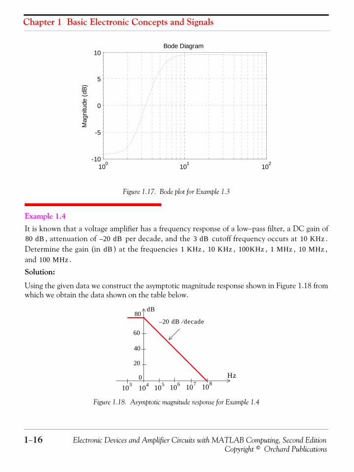
a. is this system stable?
b. use the MATLAB bode(sys,w) function to plot the magnitude of this transfer function.Solution:
a. Let us use the MATLAB solve('eqn1','eqn2',...,'eqnN') function to find the roots of the qua-dratic factors.
syms s; equ1=solve('s^2+2*s+5−0'), equ2=solve('s^2+6*s+25−0')
equ1 =[-1+2*i] [-1-2*i]
equ2 =[-3+4*i] [-3-4*i]
The zeros and poles of are shown in Figure 1.16.
* An introduction to MATLAB is included as Appendix A.
10 1– ω 102 r s⁄≤ ≤
G s( ) s
G s( ) 3 s 1–( ) s2 2s 5+ +( )
s 2+( ) s2 6s 25+ +( )---------------------------------------------------=
G s( )

Electronic Devices and Amplifier Circuits with MATLAB Computing, Second Edition 1−15Copyright © Orchard Publications
Stability
Figure 1.16. Poles and zeros of the transfer function of Example 1.3
From Figure 1.16 we observe that all poles, denoted as , lie on the left−hand half−plane andthus the system is stable. The location of the zeros, denoted as , is immaterial.
b. We use the MATLAB expand(s) symbolic function to express the numerator and denomina-tor of in polynomial form
syms s; n=expand((s−1)*(s^2+2*s+5)), d=expand((s+2)*(s^2+6*s+25))n =s^3+s^2+3*s-5
d =s^3+8*s^2+37*s+50
and thus
For this example we are interested in the magnitude only so we will use the script
num=3*[1 1 3 −5]; den=[1 8 37 50]; sys=tf(num,den);...w=logspace(0,2,100); bodemag(sys,w); grid
The magnitude plot is shown in Figure 1.17.
2– 1
1– j2+
1– j– 2
3– j– 4
3– j+ 4
G s( )
G s( ) 3 s3 s2 3s 5–+ +( )
s3 8s2 37s 50+ + +( )---------------------------------------------------=
Chapter 1 Basic Electronic Concepts and Signals
1−16 Electronic Devices and Amplifier Circuits with MATLAB Computing, Second EditionCopyright © Orchard Publications
Figure 1.17. Bode plot for Example 1.3
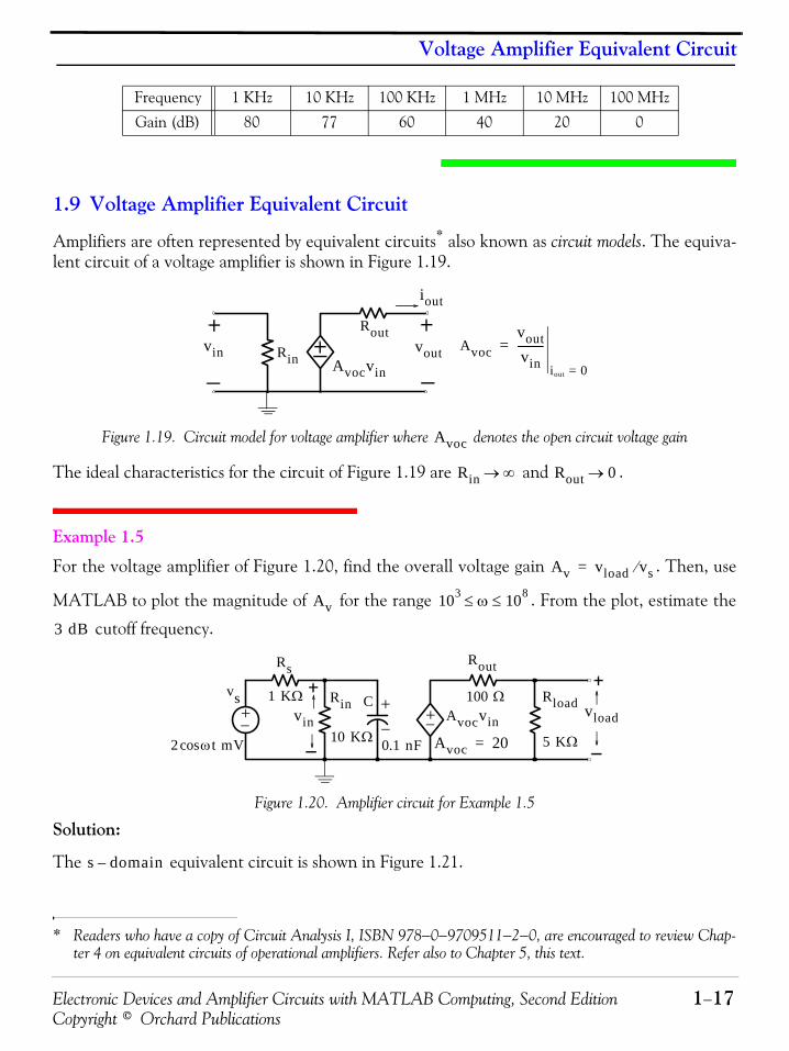
Example 1.4 It is known that a voltage amplifier has a frequency response of a low−pass filter, a DC gain of
, attenuation of per decade, and the cutoff frequency occurs at .Determine the gain (in ) at the frequencies , , , , ,and .
Solution:
Using the given data we construct the asymptotic magnitude response shown in Figure 1.18 fromwhich we obtain the data shown on the table below.
Figure 1.18. Asymptotic magnitude response for Example 1.4
100
101
102
-10
-5
0
5
10
Mag
nitu
de (
dB)
Bode Diagram
80 dB 20 dB– 3 dB 10 KHzdB 1 KHz 10 KHz 100KHz 1 MHz 10 MHz
100 MHz
dB
Hz
80
20
40
0
60
20 dB– decade⁄
108107106105104103
Electronic Devices and Amplifier Circuits with MATLAB Computing, Second Edition 1−17Copyright © Orchard Publications
Voltage Amplifier Equivalent Circuit
1.9 Voltage Amplifier Equivalent Circuit
Amplifiers are often represented by equivalent circuits* also known as circuit models. The equiva-lent circuit of a voltage amplifier is shown in Figure 1.19.
Figure 1.19. Circuit model for voltage amplifier where denotes the open circuit voltage gain
The ideal characteristics for the circuit of Figure 1.19 are and .
Example 1.5
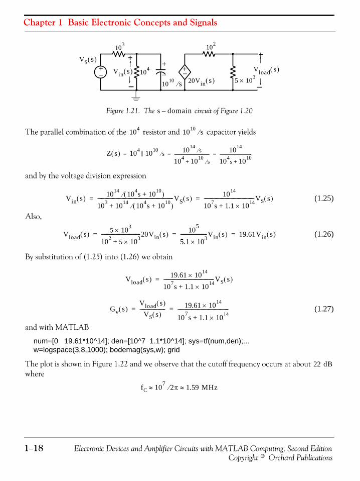
For the voltage amplifier of Figure 1.20, find the overall voltage gain . Then, use
MATLAB to plot the magnitude of for the range . From the plot, estimate the
cutoff frequency.
Figure 1.20. Amplifier circuit for Example 1.5
Solution:
The equivalent circuit is shown in Figure 1.21.
Frequency 1 KHz 10 KHz 100 KHz 1 MHz 10 MHz 100 MHz
Gain (dB) 80 77 60 40 20 0
* Readers who have a copy of Circuit Analysis I, ISBN 978−0−9709511−2−0, are encouraged to review Chap-ter 4 on equivalent circuits of operational amplifiers. Refer also to Chapter 5, this text.
vin Rin Avocvin
Rout
iout
vout Avocvoutvin----------
iout 0=
=
Avoc
Rin ∞→ Rout 0→
Av vload vs⁄=
Av 103 ω 108≤ ≤
3 dB
Rs
1 KΩ+ +
0.1 nF− −
Cvin
Rin
10 KΩ2 ωt mVcos
vs
Rout
100 Ω+− Avocvin
Avoc 20=
vloadRload
5 KΩ
s domain–
Chapter 1 Basic Electronic Concepts and Signals
1−18 Electronic Devices and Amplifier Circuits with MATLAB Computing, Second EditionCopyright © Orchard Publications
Figure 1.21. The circuit of Figure 1.20
The parallel combination of the resistor and capacitor yields
and by the voltage division expression
(1.25)
Also,
(1.26)
By substitution of (1.25) into (1.26) we obtain
(1.27)
and with MATLAB
num=[0 19.61*10^14]; den=[10^7 1.1*10^14]; sys=tf(num,den);...w=logspace(3,8,1000); bodemag(sys,w); grid
The plot is shown in Figure 1.22 and we observe that the cutoff frequency occurs at about where
++
− −+−
103 VS s( )
Vin s( ) 104 1010 s⁄ 20Vin s( )
102
Vload s( )5 103×
s domain–
104 1010 s⁄
Z s( ) 104 1010s⁄|| 1014
s⁄
104 1010s⁄+
----------------------------------- 1014
104s 1010
+--------------------------------= = =
Vin s( ) 1014 104s 1010+( )⁄
103 1014 104s 1010+( )⁄+
--------------------------------------------------------------VS s( ) 1014
107s 1.1 10× 14+
-----------------------------------------VS s( )= =
Vload s( ) 5 103×
102 5 103×+--------------------------------20Vin s( ) 105
5.1 10× 3----------------------Vin s( ) 19.61Vin s( )= = =
Vload s( ) 19.61 1014×
107s 1.1 10× 14+
-----------------------------------------VS s( )=
Gv s( )Vload s( )
VS s( )--------------------- 19.61 1014×
107s 1.1 10× 14+------------------------------------------= =
22 dB
fC 107 2π⁄ 1.59 MHz≈ ≈
Electronic Devices and Amplifier Circuits with MATLAB Computing, Second Edition 1−19Copyright © Orchard Publications
Current Amplifier Equivalent Circuit
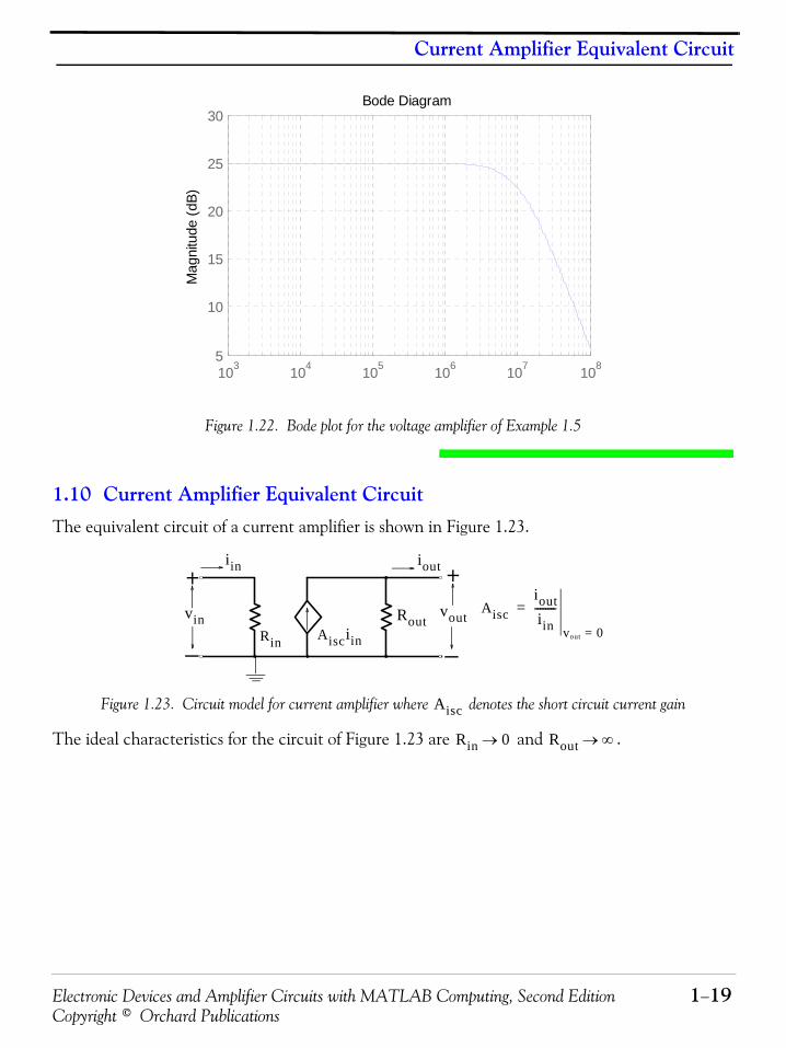
Figure 1.22. Bode plot for the voltage amplifier of Example 1.5
1.10 Current Amplifier Equivalent CircuitThe equivalent circuit of a current amplifier is shown in Figure 1.23.
Figure 1.23. Circuit model for current amplifier where denotes the short circuit current gain
The ideal characteristics for the circuit of Figure 1.23 are and .
103
104
105
106
107
108
5
10
15
20
25
30
Mag
nitu
de (
dB)
Bode Diagram
iin
Rin Aisciin
vin
iout
Routvout
Aiscioutiin--------
vout 0=
=
Aisc
Rin 0→ Rout ∞→

Chapter 1 Basic Electronic Concepts and Signals
1−20 Electronic Devices and Amplifier Circuits with MATLAB Computing, Second EditionCopyright © Orchard Publications
Example 1.6 For the current amplifier of Figure 1.24, derive an expression for the overall current gain
.
Figure 1.24. Current amplifier for Example 1.6
Solution:
Using the current division expression we obtain
(1.28)
Also, (1.29)
Substitution of (1.28) into (1.29) yields
(1.30)
or
In Sections 1.9 and 1.10 we presented the voltage and current amplifier equivalent circuits alsoknown as circuit models. Two more circuit models are the transresistance and transconductanceequivalent circuits and there are introduced in Exercises 1.4 and 1.5 respectively.
Ai iload is⁄=
is
Rs Rin
iin
Aisciin
iout
RoutRload
iload
Vload
iinRs
Rs Rin+--------------------is=
iloadRout
Rout Rload+------------------------------Aisciin=
iloadRout
Rout Rload+------------------------------Aisc
RSRS Rin+---------------------is=
Aiiload
is-----------
RoutRout Rload+------------------------------
RSRS Rin+--------------------Aisc= =

Electronic Devices and Amplifier Circuits with MATLAB Computing, Second Edition 1−21Copyright © Orchard Publications
Summary
1.11 Summary• A signal is any waveform that serves as a means of communication. It represents a fluctuating
electric quantity, such as voltage, current, electric or magnetic field strength, sound, image, orany message transmitted or received in telegraphy, telephony, radio, television, or radar.
• The average value of a waveform in the interval is defined as
• A periodic time function satisfies the expression
for all time and for all integers . The constant is the period and it is the smallest value oftime which separates recurring values of the waveform.
• An alternating waveform is any periodic time function whose average value over a period iszero.
• The effective (or RMS) value of a periodic current waveform denoted as is the current
that produces heat in a given resistor at the same average rate as a direct (constant) current and it is found from the expression
where RMS stands for Root Mean Squared, that is, the effective value or value of acurrent is computed as the square root of the mean (average) of the square of the current.
• If the peak (maximum) value of a current of a sinusoidal waveform is , then
• An amplifier is an electronic circuit which increases the magnitude of the input signal.
• An electronic (or electric) circuit which produces an output that is smaller than the input iscalled an attenuator. A resistive voltage divider is a typical attenuator.
• An amplifier can be classified as a voltage, current or power amplifier. The gain of an amplifieris the ratio of the output to the input. Thus, for a voltage amplifier
or
f t( ) a t b≤ ≤
f t( )ave ab Area
Period-----------------
f t( ) tda
b∫
b a–------------------------= =
f t( ) f t nT+( )=
t n T
i t( ) Ieff
RIdc
IRMS Ieff1T--- i2 td
0
T
∫ Ave i2( )= = =
Ieff IRMS
Ip
IRMS Ip 2( )⁄ 0.707Ip= =
Voltage Gain Output VoltageInput Voltage
-----------------------------------------=

Chapter 1 Basic Electronic Concepts and Signals
1−22 Electronic Devices and Amplifier Circuits with MATLAB Computing, Second EditionCopyright © Orchard Publications
The current gain and power gain are defined similarly.
• The ratio of any two values of the same quantity (power, voltage or current) can be expressedin decibels (dB). By definition,
The values for voltage and current ratios are
• The bandwidth is where and are the cutoff frequencies. At these fre-
quencies, and these two points are known as the 3−dB down or half−power points.
• The low−pass and high−pass filters have only one cutoff frequency whereas band−pass andband−stop filters have two. We may think that low−pass and high−pass filters have also twocutoff frequencies where in the case of the low−pass filter the second cutoff frequency is at
while in a high−pass filter it is at .
• We also recall also that the output of circuit is dependent upon the frequency when the inputis a sinusoidal voltage. In general form, the output voltage is expressed as
where is referred to as the magnitude response and is referred to as the phase
response. These two responses together constitute the frequency response of a circuit.
• The magnitude and phase responses of a circuit are often shown with asymptotic lines asapproximations and these are referred to as Bode plots.
• Two frequencies and are said to be separated by an octave if and separated
by a decade if .
• The transfer function of a system is defined as
Gv Vout Vin⁄=
Gi Gp
dB 10 Pout Pin⁄log=
dB
dBv 20 Vout Vin⁄log=
dBi 20 Iout Iin⁄log=
BW ω2 ω1–= ω1 ω2
Vout 2 2⁄ 0.707= =
ω 0= ω ∞=
Vout ω( ) Vout ω( ) e jϕ ω( )=
Vout ω( ) e jϕ ω( )
ω1 ω2 ω2 2ω1=
ω2 10ω1=
G s( )Vout s( )
Vin s( )------------------ N s( )
D s( )-----------= =
Electronic Devices and Amplifier Circuits with MATLAB Computing, Second Edition 1−23Copyright © Orchard Publications
Summary
where the numerator and denominator are as shown in the expression
• In the expression
where , the roots of the numerator are called the zeros of , and are found by letting. The roots of the denominator are called the poles of and are found by letting.
• The zeros and poles can be real and distinct, or repeated, or complex conjugates, or combina-tions of real and complex conjugates. However, in most engineering applications we are inter-ested in the nature of the poles.
• A system is said to be stable if a finite input produces a finite output. We can predict the stabil-ity of a system from its impulse response .
• Stability can easily be determined from the transfer function on the complex frequencyplane of the complex variable . A system is stable only when all poles lie on the left−hand half−plane. It is marginally stable when one or more poles lie on the axis, and unstablewhen one or more poles lie on the right−hand half−plane. However, the location of the zeros inthe is immaterial.
• We can use the MATLAB function bode(sys) to draw the Bode plot of a system where sys =tf(num,den) creates a continuous−time transfer function sys with numerator num and denomi-nator den, and tf creates a transfer function. With this function, the frequency range and numberof points are chosen automatically. The function bode(sys,{wmin,wmax}) draws the Bode plotfor frequencies between wmin and wmax (in radians/second) and the function bode(sys,w)uses the user−supplied vector w of frequencies, in radians/second, at which the Bode response isto be evaluated. To generate logarithmically spaced frequency vectors, we use the commandlogspace(first_exponent,last_exponent, number_of_values).
The bode(sys,w) function displays both magnitude and phase. If we want to display the magni-tude only, we can use the bodemag(sys,w) function.
• Amplifiers are often represented by equivalent circuits also known as circuit models. The com-mon types are the voltage amplifier, the current amplifier, the transresistance amplifier, and thetransconductance amplifier.
N s( ) D s( )
Vout s( )ansn an 1– sn 1– an 2– sn 2– … a0+ + + +( )
bmsm bm 1– sm 1– bm 2– sm 2– … b0+ + + +( )----------------------------------------------------------------------------------------------------------------Vin s( ) N s( )
D s( )-----------Vin s( )= =
F s( ) N s( )D s( )-----------
1an----- bmsm bm 1– sm 1– bm 2– sm 2– … b1s b0+ + + + +( )
sn an 1–
an------------sn 1– an 2–
an------------sn 2– …
a1an-----s
a0an-----+ + + + +
----------------------------------------------------------------------------------------------------------------------------------= =
m n< F s( )N s( ) 0= F s( )D s( ) 0=
h t( )
G s( )s σ jω+=
jω
s plane–
Chapter 1 Basic Electronic Concepts and Signals
1−24 Electronic Devices and Amplifier Circuits with MATLAB Computing, Second EditionCopyright © Orchard Publications
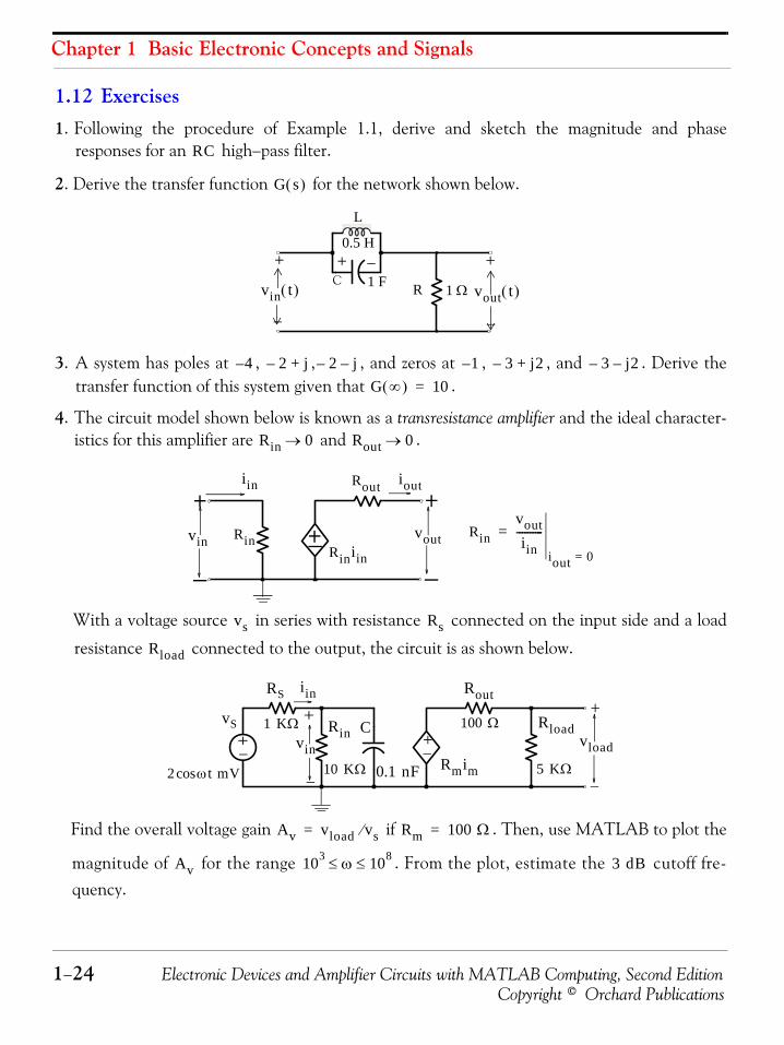
1.12 Exercises1. Following the procedure of Example 1.1, derive and sketch the magnitude and phase
responses for an high−pass filter.
2. Derive the transfer function for the network shown below.
3. A system has poles at , , , and zeros at , , and . Derive thetransfer function of this system given that .
4. The circuit model shown below is known as a transresistance amplifier and the ideal character-istics for this amplifier are and .
With a voltage source in series with resistance connected on the input side and a load
resistance connected to the output, the circuit is as shown below.
Find the overall voltage gain if . Then, use MATLAB to plot the
magnitude of for the range . From the plot, estimate the cutoff fre-quency.
RC
G s( )
L
0.5 H
C 1 F R 1 Ωvin t( )
+
−
vout t( )
+ − +
−
4– 2– j+ 2– j– 1– 3– j2+ 3– j2–
G ∞( ) 10=
Rin 0→ Rout 0→
Riniin
iout
voutvin
iin
Rin Rinvoutiin
----------iout 0=
=
Rout
vs Rs
Rload
++
+
0.1 nF− −
−
vload
vS
2 ωt mVcos
RS
1 KΩ +
−
vinC
10 KΩ
Rin
iin
Rmim
Rout
100 Ω Rload
5 KΩ
Av vload vs⁄= Rm 100 Ω=
Av 103 ω 108≤ ≤ 3 dB
Electronic Devices and Amplifier Circuits with MATLAB Computing, Second Edition 1−25Copyright © Orchard Publications
Exercises
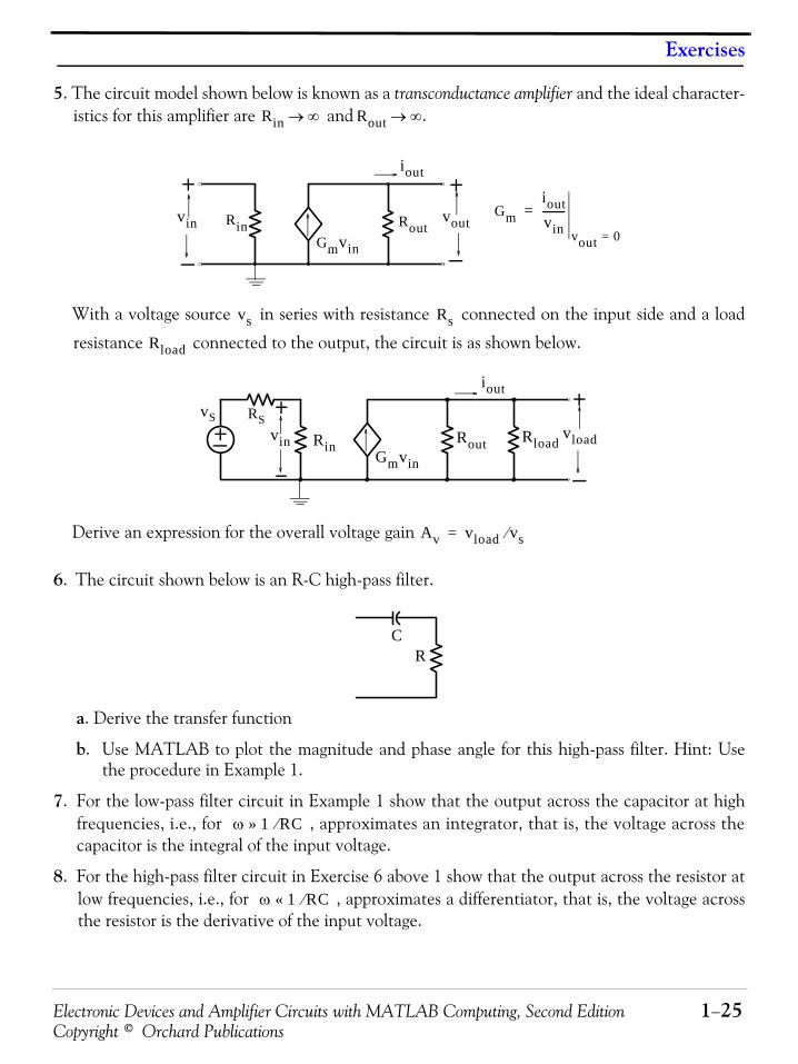
5. The circuit model shown below is known as a transconductance amplifier and the ideal character-istics for this amplifier are and .
With a voltage source in series with resistance connected on the input side and a load
resistance connected to the output, the circuit is as shown below.
Derive an expression for the overall voltage gain
6. The circuit shown below is an R-C high-pass filter.
a. Derive the transfer function
b. Use MATLAB to plot the magnitude and phase angle for this high-pass filter. Hint: Usethe procedure in Example 1.
7. For the low-pass filter circuit in Example 1 show that the output across the capacitor at highfrequencies, i.e., for , approximates an integrator, that is, the voltage across thecapacitor is the integral of the input voltage.
8. For the high-pass filter circuit in Exercise 6 above 1 show that the output across the resistor atlow frequencies, i.e., for , approximates a differentiator, that is, the voltage acrossthe resistor is the derivative of the input voltage.
Rin ∞→ Rout ∞→
vin RinGmvin
Routvout
iout
Gmioutvin--------
vout 0=
=
vs Rs
Rload
Gmvin
Rout Rloadvload
vS RSvin Rin
iout
Av vload vs⁄=
RC
ω 1 RC⁄»
ω 1 RC⁄«
Chapter 1 Basic Electronic Concepts and Signals
1−26 Electronic Devices and Amplifier Circuits with MATLAB Computing, Second EditionCopyright © Orchard Publications
1.13 Solutions to End−of−Chapter ExercisesDear Reader:
The remaining pages on this chapter contain solutions to all end−of−chapter exercises.
You must, for your benefit, make an honest effort to solve these exercises without first looking atthe solutions that follow. It is recommended that first you go through and solve those you feelthat you know. For your solutions that you are uncertain, look over your procedures for inconsis-tencies and computational errors, review the chapter, and try again. Refer to the solutions as alast resort and rework those problems at a later date.
You should follow this practice with all end−of−chapter exercises in this book.

Electronic Devices and Amplifier Circuits with MATLAB Computing, Second Edition 1−27Copyright © Orchard Publications
Solutions to End−of−Chapter Exercises
1.
or
(1)
The magnitude of (1) is
(2)
and the phase angle or argument, is
(3)
We can obtain a quick sketch for the magnitude versus by evaluating (2) at ,, and . Thus,
As ,
For ,
and as ,
We will use the MATLAB script below to plot versus radian frequency . This is shownon the plot below where, for convenience, we let .
w=0:0.02:100; RC=1; magGs=1./sqrt(1+1./(w.*RC).^2); semilogx(w,magGs); grid
We can also obtain a quick sketch for the phase angle, i.e., versus , by evaluat-ing (3) at , , , , and . Thus,
as ,
For ,
For ,
VoutR
R 1 jωC⁄+----------------------------Vin=
G jω( )VoutVin----------- jωRC
1 jωRC+------------------------ jωRC ω2R2C2
+
1 ω2R2C2+
----------------------------------------- ωRC j ωRC+( )
1 ω2R2C2+
---------------------------------------= = = =
ωRC 1 ω2R2C2+ 1 ωRC( )⁄( )atan∠
1 ω2R2C2+-------------------------------------------------------------------------------------------- 1
1 1 ω2R2C2( )⁄+--------------------------------------------- 1 ωRC( )⁄( )atan∠==
G jω( ) 1
1 1 ω2R2C2( )⁄+---------------------------------------------=
θ G jω( ){ }arg 1 ωRC⁄( )atan= =
G jω( ) ω ω 0=
ω 1 RC⁄= ω ∞→
ω 0→G jω( ) 0≅
ω 1 RC⁄=G jω( ) 1 2⁄ 0.707= =
ω ∞→G jω( ) 1≅
G jω( ) ωRC 1=
θ G jω( ){ }arg= ωω 0= ω 1 RC⁄= ω 1– RC⁄= ω ∞–→ ω ∞→
ω 0→θ 0atan– 0°≅ ≅
ω 1 RC⁄=θ 1atan– 45°–= =
ω 1– RC⁄=θ 1–( )atan– 45°= =
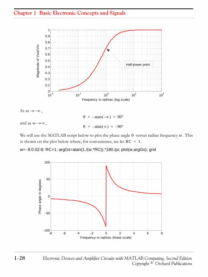
Chapter 1 Basic Electronic Concepts and Signals
1−28 Electronic Devices and Amplifier Circuits with MATLAB Computing, Second EditionCopyright © Orchard Publications
As ,
and as ,
We will use the MATLAB script below to plot the phase angle versus radian frequency . Thisis shown on the plot below where, for convenience, we let .
w=−8:0.02:8; RC=1; argGs=atan(1./(w.*RC)).*180./pi; plot(w,argGs); grid
10-2
10-1
100
101
102
0
0.1
0.2
0.3
0.4
0.5
0.6
0.7
0.8
0.9
1
Frequency in rad/sec (log scale)
Mag
nitu
de o
f V
out/
Vin
Half-power point
ω ∞–→θ ∞–( )atan– 90°= =
ω ∞→θ ∞( )atan– 90– °= =
θ ωRC 1=
-8 -6 -4 -2 0 2 4 6 8-100
-50
0
50
100
Frequency in rad/sec (linear scale)
Pha
se a
ngle
in d
egre
es
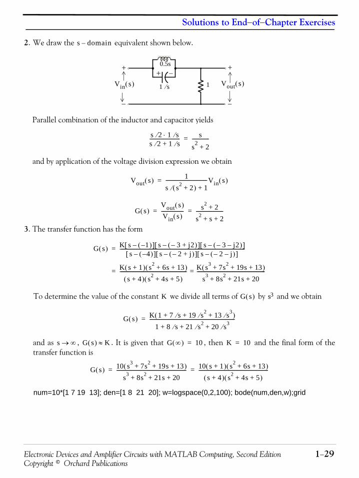
Electronic Devices and Amplifier Circuits with MATLAB Computing, Second Edition 1−29Copyright © Orchard Publications
Solutions to End−of−Chapter Exercises
2. We draw the equivalent shown below.
Parallel combination of the inductor and capacitor yields
and by application of the voltage division expression we obtain
3. The transfer function has the form
To determine the value of the constant we divide all terms of by and we obtain
and as , . It is given that , then and the final form of thetransfer function is
num=10*[1 7 19 13]; den=[1 8 21 20]; w=logspace(0,2,100); bode(num,den,w);grid
s domain–
+
−
+ −+
−
0.5s
1 s⁄Vin s( ) 1 Vout s( )
s 2⁄ 1 s⁄⋅s 2⁄ 1 s⁄+------------------------- s
s2 2+--------------=
Vout s( ) 1s s2 2+( )⁄ 1+----------------------------------Vin s( )=
G s( )Vout s( )
Vin s( )------------------ s2 2+
s2 s 2+ +----------------------= =
G s( ) K s 1–( )–[ ] s 3– j2+( )–[ ] s 3– j2–( )–[ ]s 4–( )–[ ] s 2– j+( )–[ ] s 2– j–( )–[ ]
-------------------------------------------------------------------------------------------------------=
K s 1+( ) s2 6s 13+ +( )
s 4+( ) s2 4s 5+ +( )------------------------------------------------------- K s3 7s2 19s 13+ + +( )
s3 8s2 21s 20+ + +--------------------------------------------------------==
K G s( ) s3
G s( ) K 1 7 s⁄ 19 s2⁄ 13 s3⁄+ + +( )
1 8 s⁄ 21 s2⁄ 20 s3⁄+ + +----------------------------------------------------------------------=
s ∞→ G s( ) K≈ G ∞( ) 10= K 10=
G s( ) 10 s3 7s2 19s 13+ + +( )
s3 8s2 21s 20+ + +--------------------------------------------------------- 10 s 1+( ) s2 6s 13+ +( )
s 4+( ) s2 4s 5+ +( )---------------------------------------------------------= =

Chapter 1 Basic Electronic Concepts and Signals
1−30 Electronic Devices and Amplifier Circuits with MATLAB Computing, Second EditionCopyright © Orchard Publications
4. The equivalent circuit is shown below.
The parallel combination of the resistor and capacitor yields
and by the voltage division expression
Also,
(1)
where
18
18.5
19
19.5
20
Mag
nitu
de (
dB)
100
101
102
0
5
10
15
Pha
se (
deg)
Bode Diagram
Frequency (rad/sec)
s domain–
++
+
− −
−
+
−
VS s( ) 103
Iin s( )
104 Vin s( )
+
1010 s⁄ −
102
100Iin s( ) 5 103 ×
Vload s( )
104 1010 s⁄
Z s( ) 104 1010 s⁄|| 1014 s⁄
104 1010 s⁄+---------------------------------- 1014
104s 1010+
-------------------------------= = =
Vin s( ) 1014 104s 1010+( )⁄
103 1014 104s 1010+( )⁄+
--------------------------------------------------------------VS s( ) 1014
107s 1.1 10× 14+
------------------------------------------VS s( )= =
Vload s( ) 5 103×
102 5 103×+--------------------------------100Iin s( ) 5 105×
5.1 10× 3----------------------Iin s( ) 98Iin s( )= = =
Electronic Devices and Amplifier Circuits with MATLAB Computing, Second Edition 1−31Copyright © Orchard Publications
Solutions to End−of−Chapter Exercises
and by substitution into (1) we obtain
Then,
or
and with the MATLAB script below,
num=[0 0 98]; den=[10^11 1.2*10^18 1.1*10^24]; sys=tf(num,den);...w=logspace(5,11,1000); bodemag(sys,w); grid
we obtain the Bode plot below.
This plot shows a high attenuation of the source voltage and thus the transresistance circuitmodel should not be used as a voltage amplifier.
Iin s( )Vin s( )
Z s( )----------------
1014VS s( ) 107s 1.1 10× 14+( )⁄
1014 104s 1010+( )⁄----------------------------------------------------------------------------
VS s( )
104s 1010+( ) 107s 1.1 10× 14+( )--------------------------------------------------------------------------------= = =
Vload s( ) 98104s 1010
+( ) 107s 1.1 10× 14+( )
-------------------------------------------------------------------------------VS s( )=
Gv s( )Vload s( )
VS s( )--------------------- 98
104s 1010+( ) 107s 1.1 10× 14
+( )--------------------------------------------------------------------------------= =
Gv s( )Vload s( )
VS s( )--------------------- 98
1011s2 1.2 10× 18s 1.1 1024×+ +--------------------------------------------------------------------------------= =
105
106
107
108
109
1010
1011
-640
-620
-600
-580
-560
-540
-520
-500
-480
-460
-440
Mag
nitu
de (
dB)
Bode Diagram
Frequency (rad/sec)
vs

Chapter 1 Basic Electronic Concepts and Signals
1−32 Electronic Devices and Amplifier Circuits with MATLAB Computing, Second EditionCopyright © Orchard Publications
5.
By the voltage division expression
(1)
Also, (2)
Substitution of (1) into (2) yields
6.
Application of the voltage division expression yields
or
w=1:10:100000; RC=1; ; xf=(j.*w.*RC)./(1+j.*w.*RC);...mag=20.*log10(abs(xf)); phase=angle(xf).*180./pi;... subplot(121); semilogx(w,mag); subplot(122); semilogx(w,phase)
Gmvin
Rout Rloadvload
vS RSvin Rin
iout
vinRin
RS Rin+--------------------- vS=
vloadRout Rload
Rout Rload+------------------------------- Gmvin=
vloadRout Rload
Rout Rload+------------------------------- Gm
RinRS Rin+---------------------vS=
Avvload
vS------------
RinRS Rin+---------------------
⎝ ⎠⎜ ⎟⎛ ⎞ Rout Rload
Rout Rload+-------------------------------
⎝ ⎠⎜ ⎟⎛ ⎞
Gm= =
RC
VoutR
R 1 jωC⁄+----------------------------Vin=
G jω( )VoutVin----------- jωRC
1 jωRC+------------------------= =
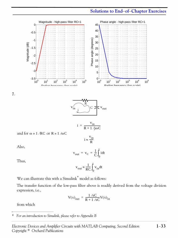
Electronic Devices and Amplifier Circuits with MATLAB Computing, Second Edition 1−33Copyright © Orchard Publications
Solutions to End−of−Chapter Exercises
7.
and for or
Also,
Thus,
We can illustrate this with a Simulink* model as follows:
The transfer function of the low-pass filter above is readily derived from the voltage divisionexpression, i.e.,
from which
* For an introduction to Simulink, please refer to Appendix B
100
101
102
103
104
105
-3.5
-3
-2.5
-2
-1.5
-1
-0.5
0
Radian frequency (log scale)
Mag
nitu
de (
dB)
Magnitude - high-pass filter RC=1
100
101
102
103
104
105
0
5
10
15
20
25
30
35
40
45
Radian frequency (log scale)
Pha
se a
ngle
(de
gree
s)
Phase angle - high-pass filter RC=1
RCvin vouti
ivin
R 1 jωC⁄+---------------------------=
ω 1 RC⁄» R 1 ωC⁄»
ivinR
-------≈
vout vC1C---- i td
0
t
∫= =
vout1
RC-------- vin td
0
t
∫≈
V s( )out1 sC⁄
R 1 sC⁄+------------------------V s( )in=
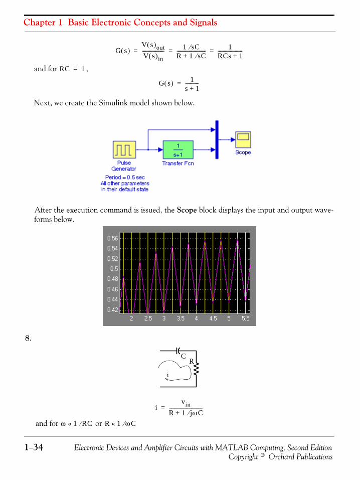
Chapter 1 Basic Electronic Concepts and Signals
1−34 Electronic Devices and Amplifier Circuits with MATLAB Computing, Second EditionCopyright © Orchard Publications
and for ,
Next, we create the Simulink model shown below.
After the execution command is issued, the Scope block displays the input and output wave-forms below.
8.
and for or
G s( )V s( )outV s( )in------------------ 1 sC⁄
R 1 sC⁄+------------------------ 1
RCs 1+--------------------= = =
RC 1=
G s( ) 1s 1+-----------=
RC
i
ivin
R 1 jωC⁄+---------------------------=
ω 1 RC⁄« R 1 ωC⁄«
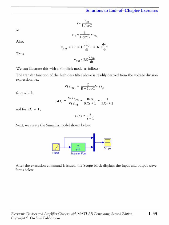
Electronic Devices and Amplifier Circuits with MATLAB Computing, Second Edition 1−35Copyright © Orchard Publications
Solutions to End−of−Chapter Exercises
or
Also,
Thus,
We can illustrate this with a Simulink model as follows:
The transfer function of the high-pass filter above is readily derived from the voltage divisionexpression, i.e.,
from which
and for ,
Next, we create the Simulink model shown below.
After the execution command is issued, the Scope block displays the input and output wave-forms below.
ivin
1 jωC⁄-----------------≈
vini
1 jωC⁄----------------- vC≈ ≈
vout iR CdvCdt
---------R RCdvCdt
---------= = =
vout RCdvindt
----------≈
V s( )outR
R 1 sC⁄+------------------------V s( )in=
G s( )V s( )outV s( )in------------------ RCs
RCs 1+-------------------- 1
RCs 1+--------------------= = =
RC 1=
G s( ) ss 1+-----------=

Chapter 1 Basic Electronic Concepts and Signals
1−36 Electronic Devices and Amplifier Circuits with MATLAB Computing, Second EditionCopyright © Orchard Publications
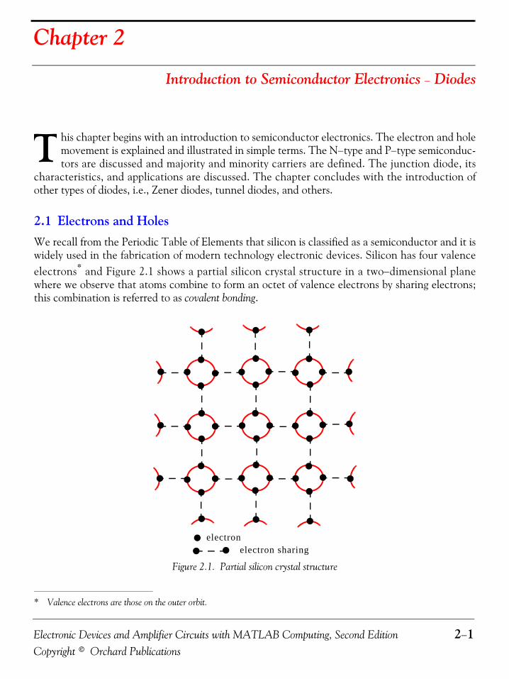
Electronic Devices and Amplifier Circuits with MATLAB Computing, Second Edition 2−1Copyright © Orchard Publications
Chapter 2
Introduction to Semiconductor Electronics − Diodes
his chapter begins with an introduction to semiconductor electronics. The electron and holemovement is explained and illustrated in simple terms. The N−type and P−type semiconduc-tors are discussed and majority and minority carriers are defined. The junction diode, its
characteristics, and applications are discussed. The chapter concludes with the introduction ofother types of diodes, i.e., Zener diodes, tunnel diodes, and others.
2.1 Electrons and HolesWe recall from the Periodic Table of Elements that silicon is classified as a semiconductor and it iswidely used in the fabrication of modern technology electronic devices. Silicon has four valenceelectrons* and Figure 2.1 shows a partial silicon crystal structure in a two−dimensional planewhere we observe that atoms combine to form an octet of valence electrons by sharing electrons;this combination is referred to as covalent bonding.
Figure 2.1. Partial silicon crystal structure
* Valence electrons are those on the outer orbit.
T
electronelectron sharing

Chapter 2 Introduction to Semiconductor Electronics − Diodes
2−2 Electronic Devices and Amplifier Circuits with MATLAB Computing, Second EditionCopyright © Orchard Publications
Thermal (heat) energy can dislodge (remove) an electron from the valence orbit of the siliconatom and when this occurs, the dislodged electron becomes a free electron and thus a vacancy(empty) space is created and it is referred to as a hole. The other electrons which stay in thevalence orbit are called bound electrons. Figure 2.2 shows a free electron that has escaped from thevalence orbit and the hole that has been created. Therefore, in a crystal of pure silicon that hasbeen thermally agitated there is an equal number of free electrons and holes.
Figure 2.2. Free electron and the created hole in a partial silicon crystal
When a free electron approaches a hole it is attracted and “captured” by that hole. Then, thatfree electron becomes once again a bound electron and this action is called recombination.Accordingly, in a silicon crystal that has been thermally agitated we have two types of currentmovement; the free electron movement and the hole movement. The movement of holes can be bestillustrated with the arrangement in Figure 2.3.
Figure 2.3. Free electron and hole movement at random
Figure 2.3 shows that a hole exists in position 1. Let us now suppose that the bound electron inposition 2 is attracted by the hole in position 1. A new hole has now been created in position 2and thus we say that the hole has moved from position 1 to position 2. Next, the hole in position
free electron hole
free electron hole1
32

Electronic Devices and Amplifier Circuits with MATLAB Computing, Second Edition 2−3Copyright © Orchard Publications
Electrons and Holes
2 may attract the bound electron from position 3 and the hole now appears in position 3. Thiscontinued process is called hole movement and it is opposite to the free electron movement.The free electron and hole movement is a random process. However, if we connect a voltagesource as shown in Figure 2.4, the hole and free electron movement takes place in an orderly fash-ion.
Figure 2.4. Free electron and hole movement when an external voltage is applied
We should keep in mind that holes are just vacancies and not positive charges although theymove the same way as positive charges. We should also remember that in both N−type and P−typematerials, current flow in the external circuit consists of electrons moving out of the negative ter-minal of the battery and into the positive terminal of the battery. Hole flow, on the other hand,only exists within the material itself.
Doping is a process where impurity atoms* which are atoms with five valence electrons such asphosphorous, arsenic, and antimony, or atoms with three valence electrons such as boron, alumi-num, and gallium, are added to melted silicon. The silicon is first melted to break down its originalcrystal structure and then impurity atoms are added. The newly formed compound then can beeither an N−type semiconductor or a P−type semiconductor depending on the impurity atoms thatwere added as shown in Figure 2.5.
Figure 2.5. N−type and P−type semiconductors
* Atoms with five valence electrons are often referred to as pentavalent atoms and atoms with three valence electrons arereferred to as trivalent atoms.
free electronhole
hole
free electron
movement
movement
free electron hole
N type semiconductor– P type semiconductor–
Si Silicon=
Si
SiSi
Si
Si
Si
Si
Si
As
As Arsenic=
Ga
Ga Gallium=

Chapter 2 Introduction to Semiconductor Electronics − Diodes
2−4 Electronic Devices and Amplifier Circuits with MATLAB Computing, Second EditionCopyright © Orchard Publications
An N−type semiconductor has more free electrons than holes and for this reason the free elec-trons are considered to be the majority carriers and the holes the minority carriers. Conversely, aP−type semiconductor has more holes than free electrons and thus the holes are the majority car-riers and the free electrons are the minority carriers.
We should remember that although the N−type material has an excess of free electrons, it is stillelectrically neutral. This is because the donor atoms in the N material were left with positivecharges (the protons outnumbered the electrons) after the free electrons became available bycovalent bonding. Therefore, for every free electron in the N material there is a correspondingpositively charged atom to balance it and the N material has a net charge of zero.
By the same reasoning, the P−type material is also electrically neutral because the excess of holesis exactly balanced by the number of free electrons.
2.2 The Junction DiodeA junction diode is formed when a piece of P−type material and a piece of N−type material arejoined together as shown in Figure 2.6 where the area between the P−type and N−type materialsis referred to as the depletion region. The depletion region is shown in more detail in Figure 2.7.
Figure 2.6. Formation of a junction diode and its symbol
Figure 2.7. The PN junction barrier formation
We would think that if we join the N and P materials together by one of the processes mentionedearlier, all the holes and electrons would pair up. This does not happen. Instead the electrons inthe N material diffuse (move or spread out) across the junction into the P material and fill some
NPA B
Depletion Region
A BP N
SymbolPhysical Structure
Junction
Depletion Region
Electrostatic Field
HoleFree ElectronNegative Ion
Positive Ion

Electronic Devices and Amplifier Circuits with MATLAB Computing, Second Edition 2−5Copyright © Orchard Publications
The Junction Diode
of the holes. At the same time, the holes in the P material diffuse across the junction into the Nmaterial and are filled by N material electrons. This process, called junction recombination, reducesthe number of free electrons and holes in the vicinity of the junction. Because there is a depletion,or lack of free electrons and holes in this area, it is known as the depletion region.
The loss of an electron from the N−type material created a positive ion in the N material, whilethe loss of a hole from the P material created a negative ion in that material. These ions are fixedin place in the crystal lattice structure and cannot move. Thus, they make up a layer of fixedcharges on the two sides of the junction as shown in Figure 2−7. On the N side of the junction,there is a layer of positively charged ions; on the P side of the junction, there is a layer of nega-tively charged ions. An electrostatic field, represented by a small battery in Figure 2−7, is estab-lished across the junction between the oppositely charged ions. The diffusion of electrons andholes across the junction will continue until the magnitude of the electrostatic field is increased tothe point where the electrons and holes no longer have enough energy to overcome it, and arerepelled by the negative and positive ions respectively. At this point equilibrium is establishedand, for all practical purposes, the movement of carriers across the junction ceases. For this rea-son, the electrostatic field created by the positive and negative ions in the depletion region iscalled a barrier.
The action just described occurs almost instantly when the junction is formed. Only the carriers inthe immediate vicinity of the junction are affected. The carriers throughout the remainder of theN and P material are relatively undisturbed and remain in a balanced condition.
If we attach a voltage source to a junction diode with the plus (+) side of the voltage source con-nected to the P−type material and the minus (−) side to the N−type as shown in Figure 2.8, a for-ward−biased PN junction is formed.
Figure 2.8. Forward−biased junction diode
When a junction diode is forward−biased, conventional current will flow in the direction of thearrow on the diode symbol.
If we reverse the voltage source terminals as shown in Figure 2.9, a reverse−biased PN junction isformed.
Figure 2.9. Reverse−biased junction diode
When a junction diode is reverse−biased, ideally no current will flows through the diode.
NP
NP

Chapter 2 Introduction to Semiconductor Electronics − Diodes
2−6 Electronic Devices and Amplifier Circuits with MATLAB Computing, Second EditionCopyright © Orchard Publications
The P−type side of the junction diode is also referred to as the anode and the N−type side as thecathode. These designations and the notations for the voltage across the diode and the cur-rent through the diode are shown in Figure 2.10 where the direction of the current
through the diode is the direction of the conventional* current flow.
Figure 2.10. Voltage and current designations for a junction diode
Figure 2.11 shows the ideal characteristics of a junction diode.
Figure 2.11. Ideal characteristics of a junction diode
With reference to Figure 2.11 we see that when , ideally , and when , ideally. However, the actual relationship in a forward−biased junction diode is the non-
linear relation
(2.1)
where and are as shown in Figure 2.10, is the reverse current, that is, the current which
would flow through the diode if the polarity of is reversed, is charge of an electron, that is,
, the coefficient varies from 1 to 2 depending on the current level andthe nature or the recombination near the junction, , that is,
* It is immaterial whether we use the electron current flow or the conventional current flow. The equations for the voltage−current relationships are the same as proved in Circuit Analysis I with MATLAB Applications, ISBN 978−0−9709511−2−0.
VD
ID ID
ID
VD
CathodeAnode
iD vD–
iD
vD
iD vD–
vD 0> iD ∞→ vD 0<
iD 0→ iD vD–
iD Ir e qvD nkT⁄( ) 1–[ ]=
iD vD Ir
vD q
q 1.6 10 19– coulomb×= nk Boltzmann's constant=
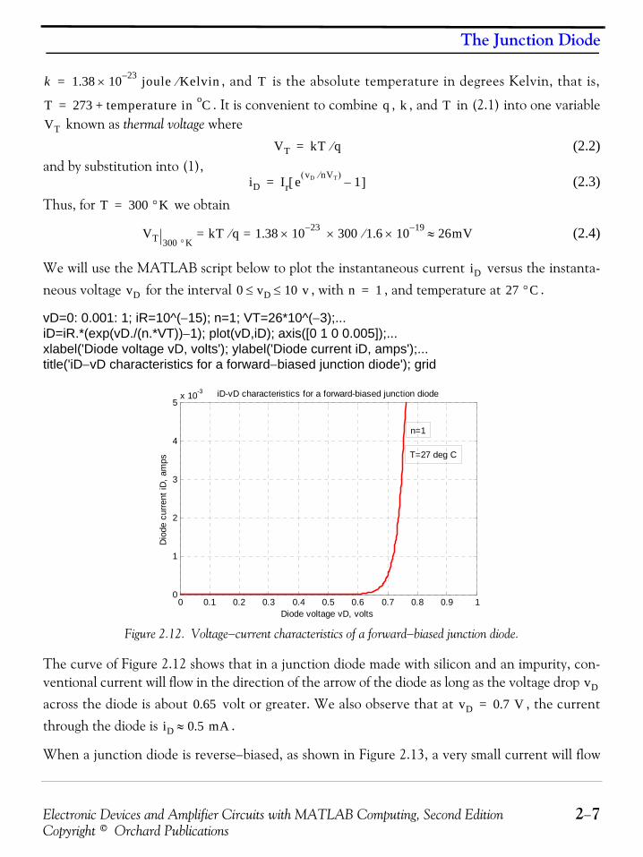
Electronic Devices and Amplifier Circuits with MATLAB Computing, Second Edition 2−7Copyright © Orchard Publications
The Junction Diode
, and is the absolute temperature in degrees Kelvin, that is,
. It is convenient to combine , , and in (2.1) into one variable known as thermal voltage where
(2.2)
and by substitution into (1),(2.3)
Thus, for we obtain
(2.4)
We will use the MATLAB script below to plot the instantaneous current versus the instanta-neous voltage for the interval , with , and temperature at .
vD=0: 0.001: 1; iR=10^(−15); n=1; VT=26*10^(−3);...iD=iR.*(exp(vD./(n.*VT))−1); plot(vD,iD); axis([0 1 0 0.005]);...xlabel('Diode voltage vD, volts'); ylabel('Diode current iD, amps');...title('iD−vD characteristics for a forward−biased junction diode'); grid
Figure 2.12. Voltage−current characteristics of a forward−biased junction diode.
The curve of Figure 2.12 shows that in a junction diode made with silicon and an impurity, con-ventional current will flow in the direction of the arrow of the diode as long as the voltage drop across the diode is about volt or greater. We also observe that at , the currentthrough the diode is .
When a junction diode is reverse−biased, as shown in Figure 2.13, a very small current will flow
k 1.38 10 23– × joule Kelvin⁄= T
T 273 temperature in Co+= q k T
VT
VT kT q⁄=
iD Ir e vD nVT⁄( ) 1–[ ]=
T 300 °K=
VT 300 °KkT q⁄ 1.38 10 23– × 300× 1.6 10 19–×⁄= = 26mV≈
iD
vD 0 vD 10 v≤ ≤ n 1= 27 °C
0 0.1 0.2 0.3 0.4 0.5 0.6 0.7 0.8 0.9 10
1
2
3
4
5x 10
-3
Diode voltage vD, volts
Dio
de c
urre
nt iD
, am
ps
iD-vD characteristics for a forward-biased junction diode
n=1
T=27 deg C
vD
0.65 vD 0.7 V=
iD 0.5 mA≈
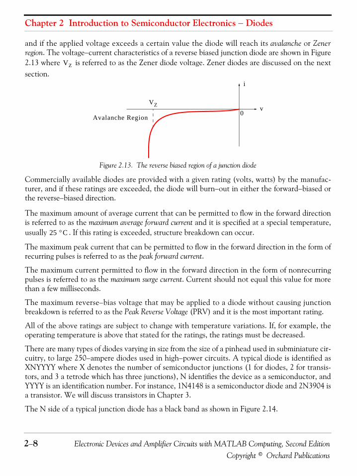
Chapter 2 Introduction to Semiconductor Electronics − Diodes
2−8 Electronic Devices and Amplifier Circuits with MATLAB Computing, Second EditionCopyright © Orchard Publications
and if the applied voltage exceeds a certain value the diode will reach its avalanche or Zenerregion. The voltage−current characteristics of a reverse biased junction diode are shown in Figure2.13 where is referred to as the Zener diode voltage. Zener diodes are discussed on the nextsection.
Figure 2.13. The reverse biased region of a junction diode
Commercially available diodes are provided with a given rating (volts, watts) by the manufac-turer, and if these ratings are exceeded, the diode will burn−out in either the forward−biased orthe reverse−biased direction.
The maximum amount of average current that can be permitted to flow in the forward directionis referred to as the maximum average forward current and it is specified at a special temperature,usually . If this rating is exceeded, structure breakdown can occur.
The maximum peak current that can be permitted to flow in the forward direction in the form ofrecurring pulses is referred to as the peak forward current.
The maximum current permitted to flow in the forward direction in the form of nonrecurringpulses is referred to as the maximum surge current. Current should not equal this value for morethan a few milliseconds.
The maximum reverse−bias voltage that may be applied to a diode without causing junctionbreakdown is referred to as the Peak Reverse Voltage (PRV) and it is the most important rating.
All of the above ratings are subject to change with temperature variations. If, for example, theoperating temperature is above that stated for the ratings, the ratings must be decreased.
There are many types of diodes varying in size from the size of a pinhead used in subminiature cir-cuitry, to large 250−ampere diodes used in high−power circuits. A typical diode is identified asXNYYYY where X denotes the number of semiconductor junctions (1 for diodes, 2 for transis-tors, and 3 a tetrode which has three junctions), N identifies the device as a semiconductor, andYYYY is an identification number. For instance, 1N4148 is a semiconductor diode and 2N3904 isa transistor. We will discuss transistors in Chapter 3.
The N side of a typical junction diode has a black band as shown in Figure 2.14.
VZ
VZ
Avalanche Region
i
v0
25 °C

Electronic Devices and Amplifier Circuits with MATLAB Computing, Second Edition 2−9Copyright © Orchard Publications
Graphical Analysis of Circuits with Non−Linear Devices
Figure 2.14. Diode symbol and orientation
Diodes are used in various applications where it is desired to have electric current flow in onedirection but to be blocked in the opposite direction as shown in Figure 2.15.
Figure 2.15. Diodes in DC Circuits
In the circuit of Figure 2.15(a) the diode is forward−biased, so current flows, and thus. In the circuit of Figure 2.15(b) the diode is reverse−biased,
no current flows, and thus .
2.3 Graphical Analysis of Circuits with Non−Linear Devices
As we’ve seen the junction diode characteristics are non−linear and thus we cannot derivethe voltage−current relationships with Ohm’s law. However, we will see later that for small signals(voltages or currents) these circuits can be represented by linear equivalent circuit models. If a cir-cuit contains only one non−linear device, such as a diode, and all the other devices are linear, wecan apply Thevenin’s theorem to reduce the circuit to a Thevenin equivalent in series with thenon−linear element. Then, we can analyze the circuit using a graphical solution. The procedure isillustrated with the following example.
Example 2.1
For the circuit of Figure 2.16, the characteristics of the diode are shown in Figure 2.17where and represent the Thevenin* equivalent voltage and resistance respectively ofanother circuit that has been reduced to its Thevenin equivalent. We wish to find the voltage across the diode and the current through this diode using a graphical solution.
* For a thorough discussion on Thevenin’s equivalent circuits, refer to Circuit Analysis I with MATLAB Applications, ISBN978−0−9709511−2−0.
A BA B
Symbol Orientation
1.5 VR
Vout
VD
ID
1.5 V R Vout 0=ID 0=
a( ) Forward biased diode– b( ) Reverse biased diode–
Vout 1.5 VD– 1.5 0.7– 0.8 V= = =
Vout 0=
i v–
i v– DVTH RTH
vD
iD
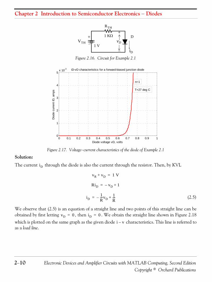
Chapter 2 Introduction to Semiconductor Electronics − Diodes
2−10 Electronic Devices and Amplifier Circuits with MATLAB Computing, Second EditionCopyright © Orchard Publications
Figure 2.16. Circuit for Example 2.1
Figure 2.17. Voltage−current characteristics of the diode of Example 2.1
Solution:
The current through the diode is also the current through the resistor. Then, by KVL
(2.5)
We observe that (2.5) is an equation of a straight line and two points of this straight line can beobtained by first letting , then . We obtain the straight line shown in Figure 2.18which is plotted on the same graph as the given diode characteristics. This line is referred toas a load line.
−
+
1 VVTH
RTH
1 KΩ +
−
vD
D
iD
0 0.1 0.2 0.3 0.4 0.5 0.6 0.7 0.8 0.9 10
1
2
3
4
5x 10
-3
Diode voltage vD, volts
Dio
de c
urre
nt iD
, am
ps
iD-vD characteristics for a forward-biased junction diode
n=1
T=27 deg C
iD
vR vD+ 1 V=
RiD vD– 1+=
iD1R----vD– 1
R----+=
vD 0= iD 0=
i v–

Electronic Devices and Amplifier Circuits with MATLAB Computing, Second Edition 2−11Copyright © Orchard Publications
Graphical Analysis of Circuits with Non−Linear Devices
Figure 2.18. Curves for determining voltage and current in the diode of Example 2.1
The intersection of the non−linear curve and the load line yields the voltage and the current of thediode where we find that and .
Check:Since this is a series circuit, also. Therefore, the voltage drop across the resistor is
. Then, by KVL
The relation of (2.3) gives us the current when the voltage is known. Quite often, we want to findthe voltage when the current is known. To do that we rewrite (2.3) as
and since , the above relation reduces to
(2.6)
or
Taking the natural logarithm of both sides we obtain
0 0.1 0.2 0.3 0.4 0.5 0.6 0.7 0.8 0.9 10
0.1
0.2
0.3
0.4
0.5
0.6
0.7
0.8
0.9
1x 10
-3
Diode voltage vD, volts
Dio
de c
urre
nt iD
, am
ps
iD-vD characteristics for a forward-biased junction diode
vD 0.68V ≈ iD 0.32 mA≈
iR 0.32 mA= vR
vR 1 KΩ 0.32 mA× 0.32 V= =
vR vD+ 0.32 0.68+ 1 V= =
iD Ir+ IrevD nVT⁄( )
=
iD Ir»
iD IrevD nVT⁄( )
=
iDIr----- e vD nVT⁄( )
=

Chapter 2 Introduction to Semiconductor Electronics − Diodes
2−12 Electronic Devices and Amplifier Circuits with MATLAB Computing, Second EditionCopyright © Orchard Publications
(2.7)
Recalling that
we obtain
and thus (2.7) may also be written as
(2.8)
Example 2.2
Derive an expression for the voltage change corresponding to a current change.
Solution:
From (2.3)
and since
Let
and
By division we obtain
Taking the natural log of both sides we obtain
vD nVT⁄iDIr-----ln=
vD nVT iD Ir⁄( )ln=
xalogxblogablog
--------------=
iD Ir⁄( )ln iD Ir⁄( )elogiD Ir⁄( )10log
e10log-------------------------------
iD Ir⁄( )10log0.4343
------------------------------- 2.3 iD Ir⁄( )10log= = = =
vD 2.3nVT iD Ir⁄( )10log=
Δv V2 V1–=
Δi I2 I1–=
iD Ir e vD nVT⁄( ) 1–[ ]=
iD Ir+ IrevD nVT⁄( )
=
iD Ir»
iD IrevD nVT⁄( )
≈
ID1 IreVD1 nVT⁄
≈
ID2 IreVD2 nVT⁄
≈
ID2ID1-------
IreVD2 nVT⁄
IreVD1 nVT⁄
------------------------≈ e VD2 VD1–( ) nVT⁄=

Electronic Devices and Amplifier Circuits with MATLAB Computing, Second Edition 2−13Copyright © Orchard Publications
Piecewise Linear Approximations
(2.9)
Example 2.3
Experiments have shown that the reverse current increases by about per rise, and it
is known that for a certain diode at . Compute at .
Solution:
This represents about increase in reverse current when the temperature rises from to.
2.4 Piecewise Linear ApproximationsThe analysis of electronic circuits that contain diodes is greatly simplified with the use of diodemodels where we approximate the diode forward−biased characteristics with two straight lines asshown in Figure 2.19.
Figure 2.19. Straight lines for forward−biased diode characteristics approximations
Using the approximation with the straight lines shown in Figure 2.19, we can now represent a typ-ical junction diode with the equivalent circuit shown in Figure 2.20.
ID2ID1-------ln e VD2 VD1–( ) nVT⁄
( )ln 1nVT---------- VD2 VD1–( )= =
Δv VD2 VD1– nVT ID2 ID1⁄( )ln 2.3nVT ID2 ID1⁄( )10log= = =
Ir 15% 1 °C
Ir 10 14– A= 27 °C Ir 52 °C
Ir 52 °C10 14– 1 0.15+( ) 52 27–( )°C 10 14– 1.15( )25 3.3 10 13– A×≈= =
97% 27 °C52 °C
0 0.1 0.2 0.3 0.4 0.5 0.6 0.7 0.8 0.9 10
0.001
0.002
0.003
0.004
0.005
0.006
0.007
0.008
0.009
0.01
Diode voltage vD, volts
Dio
de c
urre
nt iD
, am
ps
iD-vD characteristics for a forward-biased junction diode
Slope=1/rD

Chapter 2 Introduction to Semiconductor Electronics − Diodes
2−14 Electronic Devices and Amplifier Circuits with MATLAB Computing, Second EditionCopyright © Orchard Publications
Figure 2.20. Representation of a practical diode by its piecewise linear equivalent
In Figure 2.20(b), the diode represents an ideal diode whose characteristics are shown inFigure 2.21, the horizontal solid line in Figure 2.19 represents the small voltage source in Fig-ure 2.20(b), and the reciprocal of the slope of the line in Figure 2.19 is represented by the resis-tance shown in Figure 2.20(b). For convenience, these representations are also illustrated inFigure 2.21.
Figure 2.21. The components of a practical junction diode
Example 2.4
In the circuit of Figure 2.22(a) the diodes are identical and the piecewise linear characteris-tics are shown in Figure 2.22(b). Find the voltage .
Figure 2.22. Circuit and piecewise linear characteristics for Example 2.4
Solution:
In Figure 2.23 we have replaced the diodes by their piecewise linear equivalents and have com-bined the two parallel resistors. Also, for each branch we have combined the diode voltage
with the applied voltages, and .
+
ID
+ −VD rD
ID
a( ) Practical diode b( ) Piecewise linear equivalent
BA AB
i v–
VD
rD
0.65 V0 V
slope 1 rD⁄=rD
VD
i v–
Vout
1 V 2 V 3 V2 KΩ 2 KΩ Vout
v V( )
i ma( )
0.7 V
slope 50 10 3– A V⁄×=
a( ) b( )
i v–
VD 0.7 V= rD 1 slope⁄ 50 10 3– A V⁄× 20 Ω= = =

Electronic Devices and Amplifier Circuits with MATLAB Computing, Second Edition 2−15Copyright © Orchard Publications
Low Frequency AC Circuits with Junction Diodes
Figure 2.23. Piecewise linear equivalent circuit for Example 2.4
Let us follow the procedure below to find out if we can arrive to a valid answer. By Kirchoff’s Cur-rent Law (KCL)
Check:
We see that the current cannot be negative, that is, it cannot flow on the opposite direction ofthe one shown. Also, the current is zero. Therefore, we must conclude that only the diode onthe right side conducts and by the voltage division expression
2.5 Low Frequency AC Circuits with Junction Diodes
When used with AC circuits of low frequencies, diodes, usually with are biased to
Vout
I41 KΩ
20 Ω
I3
20 Ω20 Ω
I2I1
0.3 V 1.3 V 2.3 V
I1 I2 I3+ + I4=
0.3 Vout–
20------------------------
1.3 Vout–
20------------------------
2.3 Vout–
20------------------------+ +
Vout1000------------=
15 50Vout– 65 50Vout– 115 50Vout– Vout–+ +
1000-------------------------------------------------------------------------------------------------------------------------- 0=
151Vout 195=
Vout 195 151⁄ 1.29 1.3 V≈= =
I1 0.3 1.3–( ) 20⁄ 50– mA≈ ≈
I2 1.3 1.3–( ) 20⁄ 0 ≈ ≈
I3 2.3 1.3–( ) 20⁄ 50 mA≈=
I4 1.3 1000⁄ 1.3 mA= =
I1 I2 I3+ + I4≠
I1
I2
Vout1000
20 1000+------------------------ 1.3× 1.3 V≈=
1.8 n 2.0≤ ≤

Chapter 2 Introduction to Semiconductor Electronics − Diodes
2−16 Electronic Devices and Amplifier Circuits with MATLAB Computing, Second EditionCopyright © Orchard Publications
operate at some point in the neighborhood of the relatively linear region of the characteris-tics where . A bias point denoted as whose coordinates are isshown in Figure 2.24 for a junction diode with .
Figure 2.24. Junction diode biased at point Q and changes in corresponding to changes in
Figure 2.24 shows how changes in result in changes in .We can derive an expression that relates and in a junction diode. The current produced by the bias DC voltage is
(2.10)
and with an AC voltage superimposed the sum of the DC and AC voltages is
(2.11)
i v–
0.65 vD 0.8 V≤ ≤ Q Q VD ID,( )
n 2=
Q
t
t
vD t( )
iD t( )
iD vD
vD t( ) iD t( )
vD t( ) iD t( ) ID
VD
ID IreVD nVT⁄
=
vD t( ) vT t( )
vT t( ) VD vD t( )+=
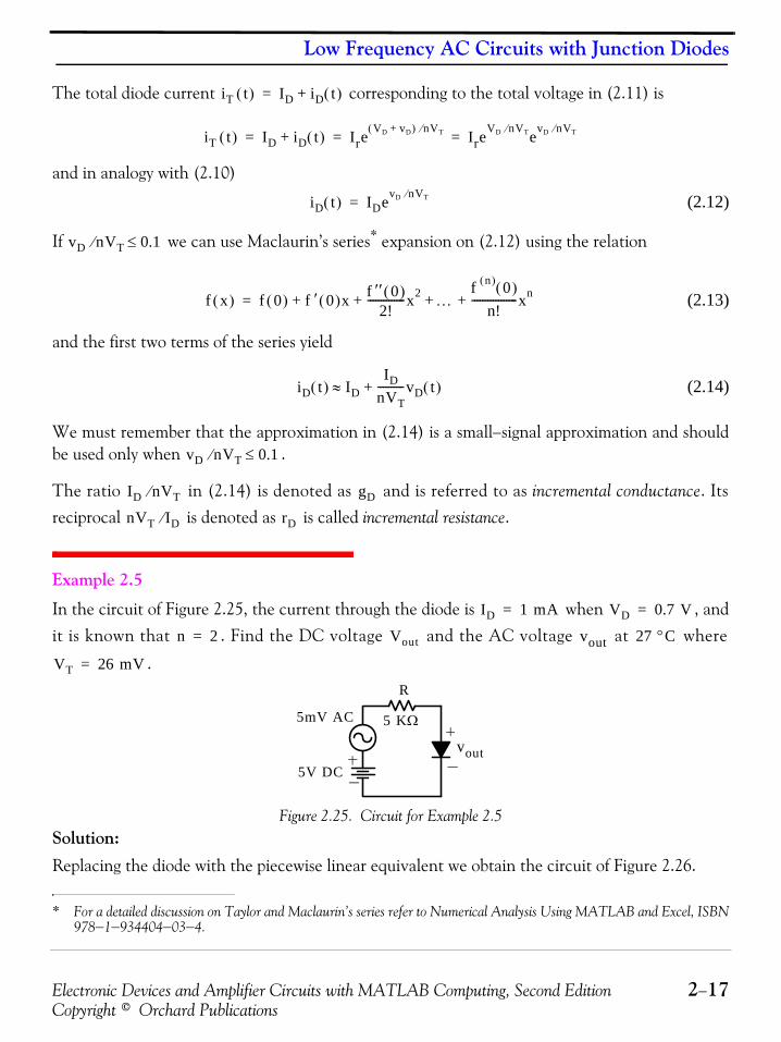
Electronic Devices and Amplifier Circuits with MATLAB Computing, Second Edition 2−17Copyright © Orchard Publications
Low Frequency AC Circuits with Junction Diodes
The total diode current corresponding to the total voltage in (2.11) is
and in analogy with (2.10)
(2.12)
If we can use Maclaurin’s series* expansion on (2.12) using the relation
(2.13)
and the first two terms of the series yield
(2.14)
We must remember that the approximation in (2.14) is a small−signal approximation and shouldbe used only when .
The ratio in (2.14) is denoted as and is referred to as incremental conductance. Itsreciprocal is denoted as is called incremental resistance.
Example 2.5
In the circuit of Figure 2.25, the current through the diode is when , andit is known that . Find the DC voltage and the AC voltage at where
.
Figure 2.25. Circuit for Example 2.5Solution:Replacing the diode with the piecewise linear equivalent we obtain the circuit of Figure 2.26.
* For a detailed discussion on Taylor and Maclaurin’s series refer to Numerical Analysis Using MATLAB and Excel, ISBN978−1−934404−03−4.
iT t( ) ID iD t( )+=
iT t( ) ID iD t( )+ IreVD vD+( ) nVT⁄ Ire
VD nVT⁄ evD nVT⁄= = =
iD t( ) IDevD nVT⁄=
vD nVT⁄ 0.1≤
f x( ) f 0( ) f ′ 0( )x f ′′ 0( )2!
--------------x2 …f n( ) 0( )
n!-----------------xn+ + + +=
iD t( ) IDID
nVT----------vD t( )+≈
vD nVT⁄ 0.1≤
ID nVT⁄ gD
nVT ID⁄ rD
ID 1 mA= VD 0.7 V=
n 2= Vout vout 27 °C
VT 26 mV=
5mV AC
5V DC
R
vout
5 KΩ

Chapter 2 Introduction to Semiconductor Electronics − Diodes
2−18 Electronic Devices and Amplifier Circuits with MATLAB Computing, Second EditionCopyright © Orchard Publications
Figure 2.26. The piecewise linear equivalent of the circuit in Example 2.5
We apply the superposition principle* for this example. We fist consider the DC voltage sourceacting alone, by suppressing (shorting out) the AC voltage source to find . Then, we con-sider the AC voltage source acting alone by suppressing (shorting out) the DC voltage source tofind . The total output voltage will be the sum of these two, that is, .
With the DC voltage source acting alone and with the assumption that , the current is
and since we are told that , by linear interpolation,
Therefore,
With the AC voltage source acting alone the value of the incremental resistance is the recip-rocal of (2.14) and thus
Then,
Therefore
* Generally, the superposition principle applies only to linear circuits. However, it is also applicable for this example since itis applied to a piecewise linear equivalent circuit.
5V DC
5mV AC
rD
vT out
R
5 KΩ
iD
Vout
vout vT out Vout vout+=
rD 5 KΩ«
ID
ID5 0.7–
5 103×----------------- 0.86mA= =
ID v 0.7V=1mA=
VD actual 0.86 0.7× 0.6 V= =
Vout 0.6 VDC=
rD
rDnVTID
---------- 2 26 10 3–××
0.86 10 3–×-------------------------------- 60.5 Ω= = =
vD peakrD
R rD+--------------- 5mV⋅ 60.5 5 10 3–××
5000 60.5+------------------------------------ 60 μVAC= = =
vT out Vout vout+ 0.6 VDC 60 μVAC+= =

Electronic Devices and Amplifier Circuits with MATLAB Computing, Second Edition 2−19Copyright © Orchard Publications
Junction Diode Applications in AC Circuits
2.6 Junction Diode Applications in AC CircuitsDiodes are also used in AC circuits where it is desired to convert AC voltages to DC voltages. Thecircuit of Figure 2.27 is a half−wave rectifier.
Figure 2.27. Half−wave rectifier circuit
In the half−wave rectifier circuit of Figure 2.27(b), the diode is forward−biased during the positivehalf−cycle from to of the input voltage and so current flows through the diode and resis-
tor where it develops an output voltage drop . For instance, if the maximum value
of is volts, the maximum value of will be . The diode is
reverse−biased during the negative half−cycle from to so no current flows, and thus.
The waveform in Figure 2.27(c) can be simulated* with the Saturation block in the model in Fig-ure 2.28.
Figure 2.28. Simulink model for creating half−rectification waveform with a saturation block
The Scope block in Figure 2.28 displays the half−rectification waveform shown in Figure 2.29.
* This and other simple Simulink models presented in this text could be parts of a large model. For a brief intro-duction to Simulink please refer to Appendix B in this text, and for a complete coverage refer to Introduction toSimulink with Engineering Applications, Second Edition, ISBN 978−1−934404−09−6.
‐1.5
‐1
‐0.5
0
0.5
1
1.5
‐0 .5
0
0 .5
1
1 .5
vD
iD
R
vin
voutπ 2π 2ππ
(a) (b) (c)
0 π vin
vout vin vD–=
vin 10 V vout vout 10 0.7– 9.3 V= =
π 2πvout 0 V=

Chapter 2 Introduction to Semiconductor Electronics − Diodes
2−20 Electronic Devices and Amplifier Circuits with MATLAB Computing, Second EditionCopyright © Orchard Publications
Figure 2.29. Half−rectification waveform displayed by the Scope block in Figure 2.28
Example 2.6
Design a DC voltmeter* that will have a volt full−scale using a milliammeter with milliamperefull−scale and internal resistance , a junction diode, and an external resistor whose valuemust be found. The input is an AC voltage with a value of volts peak−to−peak. Assume that thediode is ideal.Solution:Typically, a voltmeter is a modified milliammeter where an external resistor is connected inseries with the milliammeter as shown in Figure 2.30 where
Figure 2.30. Typical voltmeter circuit
Because the available input voltage is AC and we want to read DC (average) values, we insert ajunction diode is series as shown in Figure 2.31, and we need to find the value of so that the
* For a detailed discussion on electronic instruments refer to Circuit Analysis I with MATLAB Applications, ISBN 978−0−9709511−2−0.
10 120 Ω R
63
RV
I current through circuit=
RM internal resis cetan of milliameter=
RV external resistor in series with RM =
VM voltmeter full scale reading=
mAIM RM RV
VM+ −
= Voltmeter internal resistanceRV
= Voltmeter rangeVM
RV

Electronic Devices and Amplifier Circuits with MATLAB Computing, Second Edition 2−21Copyright © Orchard Publications
Junction Diode Applications in AC Circuits
meter will read full scale but it is now being labeled as DC.
Figure 2.31. Voltmeter for Example 2.6
Since the diode does not conduct during the negative half cycle, it follows that
and
For full−scale reading we want . Therefore,
Of course, we can label our voltmeter for any value such as , , and so on and can useany AC waveform with different peak−to−peak values.
Figure 2.32(a) shows a half−wave rectifier circuit consisting of a transformer,* a junction diode,and a load resistor, and Figure 2.32(b) shown the waveforms of the input voltage and the load
voltage .
* For a detailed discussion on transformers, refer to Circuit Analysis II with MATLAB Applications, ISBN 978−0−9709511−5−1.
1 mA 10 V
mA
IM
1 mA 20 Ω
RM RV ?=
+ −VM
Ipeak IpVp p– 2⁄RM RV+--------------------- 31.5
20 RV+-------------------= = =
IaveArea
Period-----------------
Ip tsin td0
2π
∫2π
-----------------------------
31.520 RV+------------------- tsin td
0
π
∫2π
------------------------------------------31.5 tcos–( ) 0
π
20 RV+( )2π---------------------------------- 31.5
20 RV+( )π----------------------------= = = = =
Iave 1 mA=
31.520 RV+( )π
---------------------------- 10 3–=
20 RV+31.5
π---------- 103×=
RV 10 KΩ=
50 V 100 V
vin
vload

Chapter 2 Introduction to Semiconductor Electronics − Diodes
2−22 Electronic Devices and Amplifier Circuits with MATLAB Computing, Second EditionCopyright © Orchard Publications
Figure 2.32. Half−wave rectifier circuit and input and output waveforms
When using diodes in rectifier circuits we must calculate:
a. the maximum current that the diode will allow without being damaged, and
b. The Peak Inverse Voltage (PIV) that the diode can withstand without reaching the reverse−biased breakdown region.
If the applied voltage is , then but in practice we must use diodes whosereverse−biased breakdown voltages or greater than the value of . As shown in Figure2.32(b), the diode begins conducting sometime after the input voltage shown by the dotted curverises to about . We derive the angle by which the solid curve lags the dotted curve with ref-erence to Figure 2.33* as follows.
Figure 2.33. Waveforms for the derivation of conduction angle for a half−wave rectifier
* These waveforms can be created in a Simulink model with a Sine Wave block, an Abs block, a Dead Zoneblock, and displayed in a Scope block.
+
−
vs
+
−
Rload
+
−
vload
a( )
iD
vD+ −
vload
b( )
vin
vin
vS Vp ωtsin= PIV Vp=
70% Vp
0.7 V
θ
Δv vin vout–=
θ
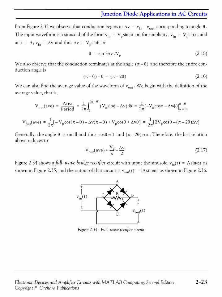
Electronic Devices and Amplifier Circuits with MATLAB Computing, Second Edition 2−23Copyright © Orchard Publications
Junction Diode Applications in AC Circuits
From Figure 2.33 we observe that conduction begins at corresponding to angle .
The input waveform is a sinusoid of the form or, for simplicity, , and
at , and thus or
(2.15)
We also observe that the conduction terminates at the angle and therefore the entire con-duction angle is
(2.16)
We can also find the average value of the waveform of . We begin with the definition of theaverage value, that is,
Generally, the angle is small and thus and . Therefore, the last relationabove reduces to
(2.17)
Figure 2.34 shows a full−wave bridge rectifier circuit with input the sinusoid asshown in Figure 2.35, and the output of that circuit is as shown in Figure 2.36.
Figure 2.34. Full−wave rectifier circuit
Δv vin vout–= θ
vin Vp ωtsin= vin Vp xsin=
x θ= vin Δv= Δv Vp θsin=
θ Δv Vp⁄1–sin=
π θ–( )
π θ–( ) θ– π 2θ–( )=
vout
Vout ave( ) AreaPeriod----------------- 1
2π------ Vp φsin Δv–( ) φd
θ
π θ–( )
∫1
2π------ Vp φcos Δvφ––( )
φ θ=
π θ–= = =
Vout ave( ) 12π------ Vp π θ–( )cos Δv π θ–( )–– Vp θcos Δvθ+ +[ ] 1
2π------ 2Vp θcos π 2θ–( )Δv–[ ]= =
θ θcos 1≈ π 2θ–( ) π≈
Vout ave( )Vpπ
------ Δv2
-------–≈
vin t( ) A ωtsin=
vout t( ) A ωtsin=
vout t( )
+
−
vin t( )
+
−
+−R
A
BC
D

Chapter 2 Introduction to Semiconductor Electronics − Diodes
2−24 Electronic Devices and Amplifier Circuits with MATLAB Computing, Second EditionCopyright © Orchard Publications
Figure 2.35. Input waveform for the circuit in Figure 2.34
Figure 2.36. Output waveform for the circuit of Figure 2.34
From Figure 2.34 we see that during the positive half cycle conventional current flows from thevoltage source to Point A, then to Point B, it goes through the resistor from Point B to Point C,and through Point D returns to the negative terminal of the voltage source. During the negativehalf cycle the lower terminal of the voltage source becomes the positive terminal, current flowsfrom Point D to Point B, it goes through the resistor from Point B to Point C, and through PointA returns to the upper (now negative) terminal of the voltage source. We observe that duringboth the positive and negative half−cycles the current enters the right terminal of the resistor,and thus is the same for both half−cycles as shown in the output waveform of Figure 2.36.
Figure 2.37 shows the input and output waveforms of the full−wave bridge rectifier on the samegraph. It is to be noted that the difference in amplitude between and is denoted as because in a full−wave bridge rectifier circuit there are two diodes in the conduction path insteadof one as shown in Figure 2.33 for the half−wave rectifier. Accordingly, lags by the angle
. Also, the output is zero for an angle centeredaround the zero crossing points.
Figure 2.37. Input and output waveforms for the full−wave bridge rectifier of Figure 2.34
FF
0
0
A
A–
vin
2ππ
00
A
π 2π
vout
vout
vin vout 2Δv
vout vin
θ 2Δv vin⁄( )1–sin= 2θ 2 2Δv vin⁄( )1–sin=
2Δv vin vout–=
2θθ

Electronic Devices and Amplifier Circuits with MATLAB Computing, Second Edition 2−25Copyright © Orchard Publications
Junction Diode Applications in AC Circuits
Figure 2.38(a) shows a full−wave rectifier with a center−tapped transformer secondary windingand Figure 2.38(b) shows the input and output waveforms.
Figure 2.38. Full−wave rectifier with centered tapped secondary winding
The waveform in Figure 2.36 can be simulated with the Saturation block in the model in Figure2.39.
Figure 2.39. Simulink model for creating full−rectification waveform with an Abs block
The Scope block in Figure 2.39 displays the half−rectification waveform shown in Figure 2.40.
Figure 2.40. Full−rectification waveform displayed by the Scope block in Figure 2.39
The output voltages from the half and full wave rectifiers are often called pulsating DC volt-ages. These voltages can be smoothed−out with the use of electric filters as illustrated with the fol-lowing example.
vload
vin
a( )
vS
+
−
+
+vin
vin−
b( )
vD
vD
+
+
−
−
+
−vload
−
vout
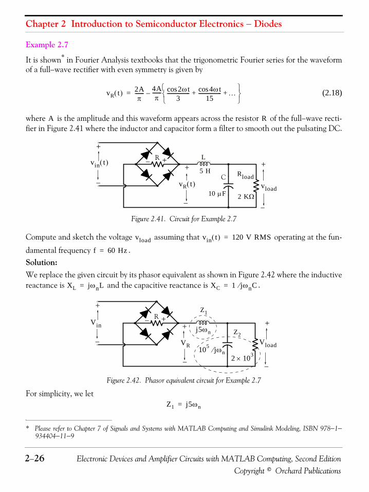
Chapter 2 Introduction to Semiconductor Electronics − Diodes
2−26 Electronic Devices and Amplifier Circuits with MATLAB Computing, Second EditionCopyright © Orchard Publications
Example 2.7
It is shown* in Fourier Analysis textbooks that the trigonometric Fourier series for the waveformof a full−wave rectifier with even symmetry is given by
(2.18)
where is the amplitude and this waveform appears across the resistor of the full−wave recti-fier in Figure 2.41 where the inductor and capacitor form a filter to smooth out the pulsating DC.
Figure 2.41. Circuit for Example 2.7
Compute and sketch the voltage assuming that operating at the fun-
damental frequency .Solution:We replace the given circuit by its phasor equivalent as shown in Figure 2.42 where the inductivereactance is and the capacitive reactance is .
Figure 2.42. Phasor equivalent circuit for Example 2.7
For simplicity, we let
* Please refer to Chapter 7 of Signals and Systems with MATLAB Computing and Simulink Modeling, ISBN 978−1−934404−11−9
vR t( ) 2Aπ
------- 4Aπ
------- 2ωtcos3
------------------ 4ωtcos15
------------------ …+ +⎩ ⎭⎨ ⎬⎧ ⎫
–=
A R
vin t( )
+
−
R +−+
−
vR t( )
L
C
10 μF
+
−2 KΩ
Rloadvload
5 H
vload vin t( ) 120 V RMS=
f 60 Hz=
XL jωnL= XC 1 jωnC⁄=
Vin
+
−
R +−+
−
+
−
VloadVR
j5ωn
Z1
105 j⁄ ωn2 103×
Z2
Z1 j5ωn=
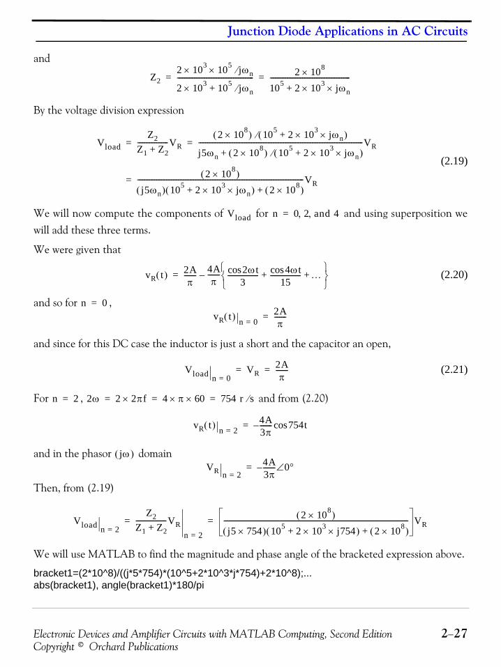
Electronic Devices and Amplifier Circuits with MATLAB Computing, Second Edition 2−27Copyright © Orchard Publications
Junction Diode Applications in AC Circuits
and
By the voltage division expression
(2.19)
We will now compute the components of for and using superposition wewill add these three terms.
We were given that
(2.20)
and so for ,
and since for this DC case the inductor is just a short and the capacitor an open,
(2.21)
For , and from (2.20)
and in the phasor domain
Then, from (2.19)
We will use MATLAB to find the magnitude and phase angle of the bracketed expression above.
bracket1=(2*10^8)/((j*5*754)*(10^5+2*10^3*j*754)+2*10^8);...abs(bracket1), angle(bracket1)*180/pi
Z22 103× 105 j⁄ ωn×
2 103× 105 j⁄ ωn+--------------------------------------------- 2 108×
105 2 103× jωn×+-----------------------------------------------= =
VloadZ2
Z1 Z2+------------------VR
2 108×( ) 105 2 103× jωn×+( )⁄
j5ωn 2 108×( ) 105 2 103× jωn×+( )⁄+-------------------------------------------------------------------------------------------------VR= =
2 108×( )
j5ωn( ) 105 2 103× jωn×+( ) 2 108×( )+--------------------------------------------------------------------------------------------------VR=
Vload n 0 2 and 4, ,=
vR t( ) 2Aπ
------- 4Aπ
------- 2ωtcos3
------------------ 4ωtcos15
------------------ …+ +⎩ ⎭⎨ ⎬⎧ ⎫
–=
n 0=vR t( ) n 0=
2Aπ
-------=
Vload n 0=VR
2Aπ
-------= =
n 2= 2ω 2 2πf× 4 π 60×× 754 r s⁄= = =
vR t( ) n 2=4A3π-------– 754tcos=
jω( )VR n 2=
4A3π-------– 0°∠=
Vload n 2=
Z2Z1 Z2+------------------VR
n 2=
2 108×( )
j5 754×( ) 105 2 103× j754×+( ) 2 108×( )+------------------------------------------------------------------------------------------------------------- VR= =
Chapter 2 Introduction to Semiconductor Electronics − Diodes
2−28 Electronic Devices and Amplifier Circuits with MATLAB Computing, Second EditionCopyright © Orchard Publications
ans = 0.0364ans = -176.0682
Therefore,
(2.22)
For , and from (2.20)
and in the phasor domain
Then, from (2.19)
We will again use MATLAB to find the magnitude and phase angle of the bracketed expressionabove.
bracket2=(2*10^8)/((j*5*1508)*(10^5+2*10^3*j*1508)+2*10^8);...abs(bracket2), angle(bracket2)*180/pi
ans = 0.0089ans = -178.0841
Therefore,
(2.23)
Combining (2.21), (2.22), and (2.23) we obtain
(2.24)
and in the time domain
Vload n 2=
Z2Z1 Z2+------------------VR
n 2=
0.0364 176.1°–∠( ) 4A3π-------– 0°∠⎝ ⎠
⎛ ⎞× 0.0154A 176.1°–∠–= = =
n 4= 4ω 4 2πf× 8 π 60×× 1 508 r s⁄,= = =
vR t( ) n 4=4A15π---------– 1508tcos=
jω( )VR n 4=
4A15π---------– 0°∠=
Vload n 4=
Z2Z1 Z2+------------------VR
n 4=
2 108×( )
j5 1508×( ) 105 2 103× j1508×+( ) 2 108×( )+------------------------------------------------------------------------------------------------------------------- VR= =
Vload n 4=
Z2Z1 Z2+------------------VR
n 4=
0.089 178.1°–∠( ) 4A15π---------– 0°∠⎝ ⎠
⎛ ⎞× 0.00076 178.1°–∠–= = =
Vload Vload n 0=Vload n 2=
Vload n 4=+ +=
A 2 π⁄ 0.0154 176.1°–∠ 0.00076A 178.1°–∠––( )=

Electronic Devices and Amplifier Circuits with MATLAB Computing, Second Edition 2−29Copyright © Orchard Publications
Junction Diode Applications in AC Circuits
(2.25)
This is the filtered output voltage across the resistor.
Let us plot (2.25) using MATLAB with and .
t=0: 1: 2000; vL=20.*(2./pi−0.0154.*cos(2.*377.*t−176.1.*pi./180)...−0.00076.*cos(4.*377.*t−178.1.*pi./180)); plot(t,vL); axis([0 2000 0 20]); hold on;...plot(t,(40/pi−0.0154)); axis([0 2000 0 20]); xlabel('Time (sec)');...ylabel('Load voltage (vL)'); title('Filtered output voltage for Example 2.7'); grid
The plot is shown in Figure 2.43 and we observe that the ripple is approximately about theaverage (DC) value.
Figure 2.43. Voltage across the resistor in Figure 2.42
The waveform in Figure 2.43 can be simulated with the Simulink model in Figure 2.44. The value must be entered at the MATLAB command prompt.
vload t( ) A 2 π⁄ 0.0154 2ωt 176.1°–( )cos 0.00076 4ωt 178.1–( )cos––( )=
2 KΩ
A 20= ω 377=
0.5 V±
0 500 1000 1500 20000
5
10
15
20
Time (sec)
Load
vol
tage
(vL
)
Filtered output voltage for Example 2.7
2 KΩ
A 20=
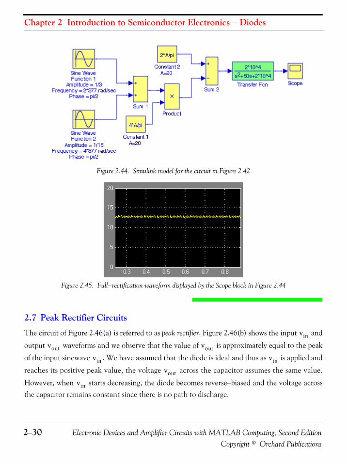
Chapter 2 Introduction to Semiconductor Electronics − Diodes
2−30 Electronic Devices and Amplifier Circuits with MATLAB Computing, Second EditionCopyright © Orchard Publications
Figure 2.44. Simulink model for the circuit in Figure 2.42
Figure 2.45. Full−rectification waveform displayed by the Scope block in Figure 2.44
2.7 Peak Rectifier Circuits
The circuit of Figure 2.46(a) is referred to as peak rectifier. Figure 2.46(b) shows the input and
output waveforms and we observe that the value of is approximately equal to the peak
of the input sinewave . We have assumed that the diode is ideal and thus as is applied and
reaches its positive peak value, the voltage across the capacitor assumes the same value.
However, when starts decreasing, the diode becomes reverse−biased and the voltage acrossthe capacitor remains constant since there is no path to discharge.
vin
vout vout
vin vin
vout
vin

Electronic Devices and Amplifier Circuits with MATLAB Computing, Second Edition 2−31Copyright © Orchard Publications
Peak Rectifier Circuits
Figure 2.46. Peak rectifier circuit
The peak rectifier circuit shown in Figure 2.46(a) will behave like an AC to DC converter if we adda resistor across the capacitor as shown in Figure 2.47(a). Then, assuming that the diode is idealand that the time constant is much greater than the discharge interval, the voltage acrossthe resistor−capacitor combination will be as shown in Figure 2.47(b).
Figure 2.47. Peak rectifier used as an AC to DC converter
From the waveforms of Figure 2.47(b) se see that peak−to−peak ripple voltage can be
made sufficiently small by choosing the time constant much larger that the period ,that is, . Also, from Figure 2.47(b) we see that the average output voltage whenthe diode conducts is
(2.26)
Next, we need to find an expression for when the diode does not conduct.
We recall from basic circuit theory* that in an simple RC circuit the capacitor voltage dis-charges as the decaying exponential
(2.27)
or(2.28)
* Please refer to Circuit Analysis I with MATLAB Applications, ISBN 978−0−9709511−2−0.
+
−vout
a( ) b( )
vin
vin
vout
τ RC=
b( )
Vpp ripple( )
t
T period( )
voutvin Vp ωtsin=
iD
+ −
R iRC
+
−
iC
a( )
voutvin
Vpp ripple( )
τ RC= TRC T» Vout ave( )
Vout ave( ) Vp12---Vpp ripple( )–=
Vpp ripple( )
vC
vC vout Vpe t RC⁄( )–= =
vout Vp Vpp ripple( )– Vpe t RC⁄( )–= =

Chapter 2 Introduction to Semiconductor Electronics − Diodes
2−32 Electronic Devices and Amplifier Circuits with MATLAB Computing, Second EditionCopyright © Orchard Publications
and since we want , we can simplify (2.28) by recalling that
and for small ,
Therefore, we can express (2.28) as
or(2.29)
and from (2.29) we observe that for to be small, we must make
2.8 Clipper CircuitsClipper (or limiter) circuits consist of diodes, resistors, and sometimes DC sources to clip or limitthe output to a certain level. Clipper circuits are used in applications where it is necessary to limitthe input to another circuit so that the latter would not be damaged.
The input−output characteristics of clipper circuits are typically those of the forward−biased andreverse−biased diode characteristics except that the output is clipped to a a certain level. Figure2.48 shows a clipper circuit and its input−output characteristics where the diode does not con-duct for and so . The diode conducts for and thus
.
Figure 2.48. Circuit where when diode does not conduct and when
Figure 2.49 shows a clipper circuit and its input−output characteristics where the diode does notconduct for but it conducts for and thus .
RC T»
e x– 1 x– x2
2!----- x3
3!-----–+= …+
xe x– 1 x–≈
Vpp ripple( ) Vp Vpe t RC⁄( )–– Vp 1 e t RC⁄( )––( ) Vp 1 1– TRC--------–⎝ ⎠
⎛ ⎞–⎝ ⎠⎛ ⎞= = =
Vpp ripple( ) VpT
RC--------=
Vpp ripple( ) RC T»
vin 0.6 V< vout vin= vin 0.7 V≥
vout 0.7 V≈
+
−
R+
−
vout
vin
0.7 V
vin vout
vout vin= vout 0.7 V≈ vin 0.7 V≥
vin 0.6– V> vin 0.7 V≤ vout 0.7– V≈
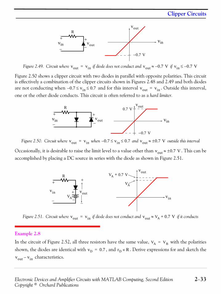
Electronic Devices and Amplifier Circuits with MATLAB Computing, Second Edition 2−33Copyright © Orchard Publications
Clipper Circuits
Figure 2.49. Circuit where if diode does not conduct and if
Figure 2.50 shows a clipper circuit with two diodes in parallel with opposite polarities. This circuitis effectively a combination of the clipper circuits shown in Figures 2.48 and 2.49 and both diodesare not conducting when and for this interval . Outside this interval,one or the other diode conducts. This circuit is often referred to as a hard limiter.
Figure 2.50. Circuit where when and outside this interval
Occasionally, it is desirable to raise the limit level to a value other than . This can beaccomplished by placing a DC source in series with the diode as shown in Figure 2.51.
Figure 2.51. Circuit where if diode does not conduct and if it conducts
Example 2.8
In the circuit of Figure 2.52, all three resistors have the same value, with the polarities
shown, the diodes are identical with , and . Derive expressions for and sketch the characteristics.
vin−
R
−
vout
−
vinvout
0.7– V
+ +
vout vin= vout 0.7– V≈ vin 0.7– V≤
0.7 vin 0.7≤ ≤– vout vin=
vin+
−
R
−
vout−
vinvout
0.7 V
− 0.7– V
+
vout vin= 0.7 vin 0.7≤ ≤– vout 0.7± V≈
vout 0.7± V≈
+
−
R+
−
vout
−
vinVA
−VA
VA 0.7 V+
+
−
voutvin
vout vin= vout VA 0.7+ V≈
VA VB=
vD 0.7= rD R«
vout vin–

Chapter 2 Introduction to Semiconductor Electronics − Diodes
2−34 Electronic Devices and Amplifier Circuits with MATLAB Computing, Second EditionCopyright © Orchard Publications
Figure 2.52. Circuit for Example 2.8Solution:
Diode conducts when and under this condition diode does not conduct. Then,
(2.30)
and
(2.31)
Diode conducts when and under this condition diode does not conduct. Then,
in accordance with the passive sign convention* we obtain
(2.32)
and
(2.33)
For range , , and the characteristics are shown in Figure2.53.
Figure 2.53. The characteristics for the circuit of Example 2.8
* Please refer to Circuit Analysis I with MATLAB Applications, ISBN 978−0−9709511−2−0.
+
−
R+
−
vin
R R
VA VB
+
−
D1 D2
ID1 ID2
+−
vout
D1 vin VA> D2
ID1vin VA vD+( )–
R R+-------------------------------------
vin VA– 0.7–
2R---------------------------------= =
vout1 0.7 VA+= RID1+ 0.7 VA Rvin VA– 0.7–( )
2R--------------------------------------+ + 0.5 vin VA 0.7+ +( )= =
D2 vin V– B< D1
ID2vin VB vD–( )–
R R+-------------------------------------–
vin VB– 0.7+
2R----------------------------------–= =
vout2 0.7– VB–= R– ID1 0.7– VB– R–vin VB– 0.7+
2R----------------------------------–⎝ ⎠
⎛ ⎞ 0.5 vin VB– 0.7–( )= =
VB– vin VA< < vout vin= vout vin–
vout
−vout1
− vout2–
vin
vout vin–

Electronic Devices and Amplifier Circuits with MATLAB Computing, Second Edition 2−35Copyright © Orchard Publications
DC Restorer Circuits
2.9 DC Restorer CircuitsA DC restorer (or clamped capacitor) is a circuit that can restore a DC voltage to a desired DClevel. The circuit of Figure 2.54 is a DC restorer and its operation can be best illustrated with thefollowing example.
Example 2.9
In the circuit of Figure 2.54, the input is as shown in Figure 2.55. Compute and sketch the
waveform for the output .
Figure 2.54. DC Restorer circuit
Figure 2.55. Input waveform for the circuit of Example 2.9
Solution:
From the circuit of Figure 2.54 we observe that the diode conducts only when and thus the
capacitor charges to the negative peak of the input which for this example is , and the capac-itor voltage is with polarity as shown in Figure 2.54. We observe that there is no pathfor the capacitor to discharge and therefore always. Since , when
, and the output has shifted upwards to zero volts as shown in Fig-
ure 2.56. When the input voltage is positive, , and . The waveformfor the output voltage is as shown in Figure 2.56.
vin
vout
+−
vout
C+
−
iD+−vin
t
vin V( )
5–
5
vin 0<
5 V–
vC 5 V=
vC 5 V= vout vin vC+=
vin 5 V–= vout 5– 5+ 0= =
vin 5 V= vout 5 5+ 10 V= =
Chapter 2 Introduction to Semiconductor Electronics − Diodes
2−36 Electronic Devices and Amplifier Circuits with MATLAB Computing, Second EditionCopyright © Orchard Publications
Figure 2.56. Output waveform for the circuit of Example 2.9
2.10 Voltage Doubler CircuitsThe circuit of Figure 2.57 is referred to as a voltage doubler.
Figure 2.57. A voltage doubler circuit
With reference to the circuits of Figures 2.46 and 2.54, we observe that the circuit of Figure 2.57is a combination of a DC restorer circuit consisting of the capacitor and diode and a peakrectifier consisting of and diode . During the positive half−cycle of the input waveformdiode conducts, the peak value of the input appears across the capacitor of and
thus . During the negative half−cycle of the input waveform diode conducts, capaci-tor is being charged to a voltage which is the sum of and and thus the output voltage
is as shown in Figure 2.58.
Figure 2.58. Output waveform for the voltage doubler circuit of Figure 2.57
t
vout V( )10
+ −
C1D1 vD1
D2
C2
vout 2– vin=
+
−
+
−vin Vp ωtsin=
C1 D1
C2 D2
D1 Vp vin C1
vD1 0= D2
C2 vin vC1
vout vin vC1+ Vp ωtsin Vp ωtsin–– 2Vp ωtsin– 2vin–= = = =
vout
t
Vp–
0
2Vp–
Electronic Devices and Amplifier Circuits with MATLAB Computing, Second Edition 2−37Copyright © Orchard Publications
Diode Applications in Amplitude Modulation (AM) Detection Circuits
Voltage triplers and voltage quadruplers can also be formed by adding more diodes and capacitor to avoltage doubler.
2.11 Diode Applications in Amplitude Modulation (AM) Detection CircuitsJunction diodes are also used in AM radio signals to remove the lower envelope of a modulatedsignal. A typical AM Envelope Detector circuit is shown in Figure 2.59. It is beyond the scope ofthis text to describe the operation of this circuit; it is described in electronic communications sys-tems books. Our intent is to show the application of the junction diode in such circuits.
Figure 2.59. Typical AM Envelope Detector circuit
The operation of an AM audio frequency signal is shown in Figure 2.60 where the magnitude of is always less than ; hence the envelope of the modulated wave never drops to zero. The
waveform of the envelope of the modulated signal is the same as the waveform of the modulatingsignal . Thus if the information in the modulated carrier is to be preserved, the waveform ofthe envelope must be preserved. The information can be recovered by recovering the waveform ofthe envelope; the peak rectifier circuit is used for this purpose. The peak rectifier is also known asdiode detector, and in this application it is frequently called an envelope detector. . The dioderemoves the lower envelope and the upper envelope. In the circuit of Figure 2.59 capacitor
and resistor form a high−pass filter that removes the carrier frequency.
Figure 2.60. Input and output signals for the circuit of Figure 2.59
2.12 Diode Applications in Frequency Modulation (FM) Detection CircuitsFigure 2.61 shows how junction diodes can be used in FM circuits. This circuit is known as the
+
−
C1 R1
C2R2
+
−
voutvin
vm t( ) VC
vm t( )
vm
C2
R2
vm t( )
t t
vC t( )
Modulating signal
Carrier Envelope
Chapter 2 Introduction to Semiconductor Electronics − Diodes
2−38 Electronic Devices and Amplifier Circuits with MATLAB Computing, Second EditionCopyright © Orchard Publications
Foster−Seely discriminator and it is used to remove the carrier, which varies in accordance with theinput audio frequency, and produce the audio frequency at its output.
Figure 2.61. Foster−Seely discriminator circuit
2.13 Zener DiodesBy special manufacturing processes the reverse voltage breakdown of a diode can be made almostvertical as shown on the characteristics curve of Figure 2.62.
Figure 2.62. Zener diode operating region
These diodes are called Zener diodes and they are designed to operate in the breakdown region.The Zener diode is always connected as a reverse−biased diode and its voltage rating and themaximum power it can absorb are given by the manufacturer. The Zener diode symbol is shownin Figure 2.63.
Figure 2.63. Symbol for a Zener diode
Zener diodes from small voltage ratings of 5 volts to large voltage ratings of 250 volts are com-mercially available and we can calculate the maximum current that a Zener diode can withstandfrom its voltage and power ratings. For instance, a 2 watt, 25 volt Zener diode can withstand amaximum current of 80 milliamperes.
AudioFrequency
Frequency modulated carrier
i v–
VZ 0
i
v
VZ
+
−IZ
VZ
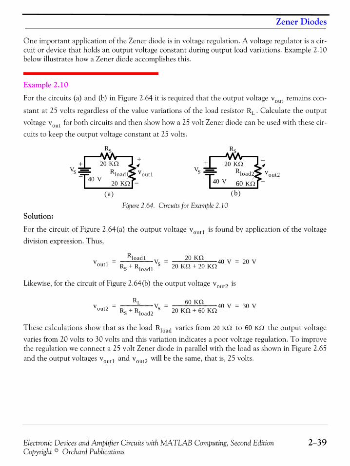
Electronic Devices and Amplifier Circuits with MATLAB Computing, Second Edition 2−39Copyright © Orchard Publications
Zener Diodes
One important application of the Zener diode is in voltage regulation. A voltage regulator is a cir-cuit or device that holds an output voltage constant during output load variations. Example 2.10below illustrates how a Zener diode accomplishes this.
Example 2.10
For the circuits (a) and (b) in Figure 2.64 it is required that the output voltage remains con-
stant at 25 volts regardless of the value variations of the load resistor . Calculate the outputvoltage for both circuits and then show how a 25 volt Zener diode can be used with these cir-cuits to keep the output voltage constant at 25 volts.
Figure 2.64. Circuits for Example 2.10
Solution:
For the circuit of Figure 2.64(a) the output voltage is found by application of the voltagedivision expression. Thus,
Likewise, for the circuit of Figure 2.64(b) the output voltage is
These calculations show that as the load varies from to the output voltagevaries from 20 volts to 30 volts and this variation indicates a poor voltage regulation. To improvethe regulation we connect a 25 volt Zener diode in parallel with the load as shown in Figure 2.65and the output voltages and will be the same, that is, 25 volts.
vout
RL
vout
a( ) b( )
40 VVS
+ +
− −
RS
20 KΩ
20 KΩ
+
−
vout1Rload1VS
40 V
RS
20 KΩ
60 KΩ
Rload2 vout2
+
−
vout1
vout1Rload1
RS Rload1+----------------------------VS
20 KΩ20 KΩ 20 KΩ+--------------------------------------40 V 20 V= = =
vout2
vout2RL
RS Rload2+----------------------------VS
60 KΩ20 KΩ 60 KΩ+--------------------------------------40 V 30 V= = =
Rload 20 KΩ 60 KΩ
vout1 vout2
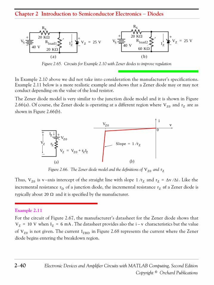
Chapter 2 Introduction to Semiconductor Electronics − Diodes
2−40 Electronic Devices and Amplifier Circuits with MATLAB Computing, Second EditionCopyright © Orchard Publications
Figure 2.65. Circuits for Example 2.10 with Zener diodes to improve regulation
In Example 2.10 above we did not take into consideration the manufacturer’s specifications.Example 2.11 below is a more realistic example and shows that a Zener diode may or may notconduct depending on the value of the load resistor.
The Zener diode model is very similar to the junction diode model and it is shown in Figure2.66(a). Of course, the Zener diode is operating at a different region where and are asshown in Figure 2.66(b).
Figure 2.66. The Zener diode model and the definitions of and
Thus, is −axis intercept of the straight line with slope and . Like theincremental resistance of a junction diode, the incremental resistance of a Zener diode istypically about and it is specified by the manufacturer.
Example 2.11 For the circuit of Figure 2.67, the manufacturer’s datasheet for the Zener diode shows that
when . The datasheet provides also the characteristics but the valueof is not given. The current in Figure 2.68 represents the current where the Zenerdiode begins entering the breakdown region.
a( ) b( )
VS40 V
+ +
− −
RS
20 KΩ
20 KΩ
Rload1 IZ IZ
+VZ 25 V= −VS
40 V60 KΩ
Rload2
20 KΩ
RS
+
−VZ 25 V=
VZ0 rZ
+
VZ
−
VZ0+−
IZ
rZVZ VZ0 rZIZ+=
VZ0
Slope 1 rZ⁄=
0
iv
(a) (b)
VZ0 rZ
VZ0 v 1 rZ⁄ rZ Δv Δi⁄=
rD rZ
20 Ω
VZ 10 V= IZ 6 mA= i v–
VZ0 IZBD

Electronic Devices and Amplifier Circuits with MATLAB Computing, Second Edition 2−41Copyright © Orchard Publications
Zener Diodes
Figure 2.67. Circuit for Example 2.11
Figure 2.68. Graph for Example 2.11
Compute:
a. The output voltage if the load resistor is disconnected.
b. The output voltage if the load resistor is connected and adjusted to .
c. The output voltage if the load resistor is connected and adjusted to .
d. The minimum value of the load resistor for which the Zener diode will be conducting inthe breakdown region.
Solution:
a.From Figure 2.66(a),
(2.34)
and replacing the Zener diode by its equivalent we obtain the circuit shown in Figure 2.69where the slope is
24 V
+
−VS
RS
1 KΩIZ
VZRload
+
−Vload
+
−
VZ0
Slope ΔiΔv------- 0.04= =
0i
v
IZBD 0.3 mA=
Vload Rload
Vload Rload 1 KΩ
Vload Rload 200 Ω
Rload
VZ VZ0 rZIZ+=
1 rZ⁄ Δi Δv⁄ 0.04= =
rZ Δv Δi⁄ 1 0.04⁄ 25 Ω= = =

Chapter 2 Introduction to Semiconductor Electronics − Diodes
2−42 Electronic Devices and Amplifier Circuits with MATLAB Computing, Second EditionCopyright © Orchard Publications
Figure 2.69. Zener diode replaced by its equivalent circuit and the load is disconnected
From (2.34),
and
Thus
b.
When the load resistor is connected and adjusted to the circuit is as shown in Figure2.70.
Figure 2.70. Circuit of Example 2.11 with load resistor connected and adjusted to
We will assume that the Zener diode still operates well within the breakdown region so thatthe addition of the load resistor does not change the output voltage significantly. Then,
This means that the Zener diode current will be reduced to
and thus the output voltage will be
24 VVS
+
−
RS
1 KΩ + +−
−
rZ
VZ0
IZ
Vload
VZ0 VZ rZIZ– 10 25 6 10 3–××– 8.5 V= = =
IZVS VZ0–
RS rZ+-------------------- 24 8.5–
1000 25+------------------------ 15.2 mA= = =
vout VZ0 rZIZ+ 8.5 25 15.2 10 3–××+ 8.8 V= = =
1 KΩ
VS24 V
++
+RS
1 KΩ
−−
−
Rload
1 KΩ
Iload
IZ
VloadrZ
VZ0
1 KΩ
IloadVloadRload-------------≈ 8.8
103-------- 8.8 mA= =
IZ
I 'Z 15.2 8.8– 6.4mA= =
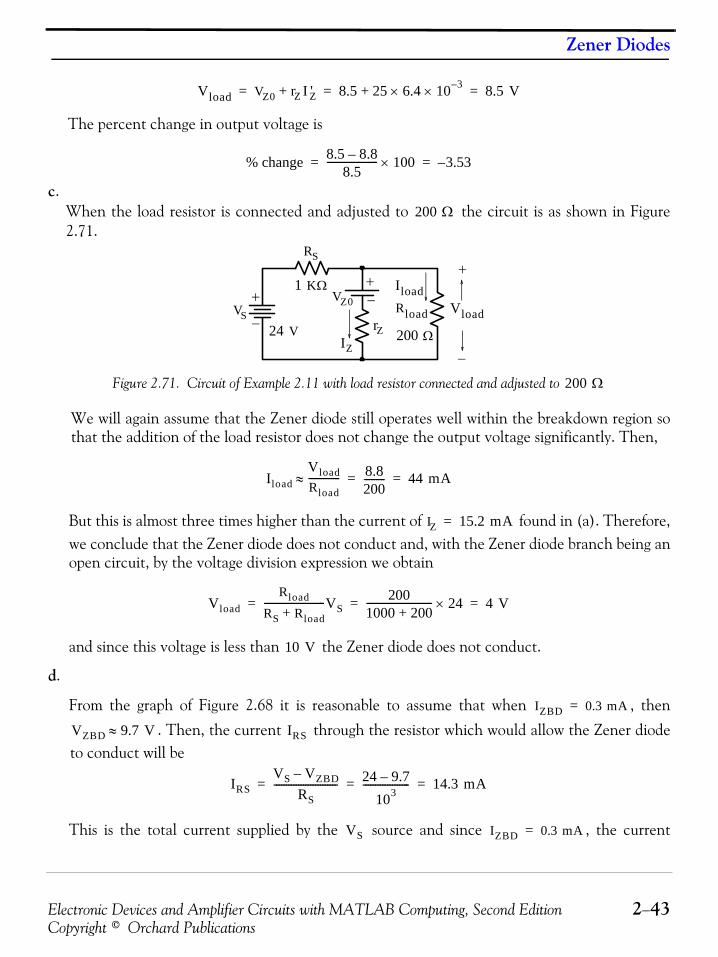
Electronic Devices and Amplifier Circuits with MATLAB Computing, Second Edition 2−43Copyright © Orchard Publications
Zener Diodes
The percent change in output voltage is
c.When the load resistor is connected and adjusted to the circuit is as shown in Figure2.71.
Figure 2.71. Circuit of Example 2.11 with load resistor connected and adjusted to
We will again assume that the Zener diode still operates well within the breakdown region sothat the addition of the load resistor does not change the output voltage significantly. Then,
But this is almost three times higher than the current of found in (a). Therefore,we conclude that the Zener diode does not conduct and, with the Zener diode branch being anopen circuit, by the voltage division expression we obtain
and since this voltage is less than the Zener diode does not conduct.
d.
From the graph of Figure 2.68 it is reasonable to assume that when , then
. Then, the current through the resistor which would allow the Zener diodeto conduct will be
This is the total current supplied by the source and since , the current
Vload VZ0 rZ I 'Z+ 8.5 25 6.4 10 3–××+ 8.5 V= = =
% change 8.5 8.8–8.5
--------------------- 100× 3.53–= =
200 Ω
VS24 V
++
+RS
1 KΩ
−
−
−
Rload
200 Ω
Iload
IZ
VloadrZ
VZ0
200 Ω
IloadVloadRload-------------≈ 8.8
200--------- 44 mA= =
IZ 15.2 mA=
VloadRload
RS Rload+-------------------------VS
2001000 200+--------------------------- 24× 4 V= = =
10 V
IZBD 0.3 mA=
VZBD 9.7 V≈ IRS
IRSVS VZBD–
RS-------------------------- 24 9.7–
103------------------- 14.3 mA= = =
VS IZBD 0.3 mA=
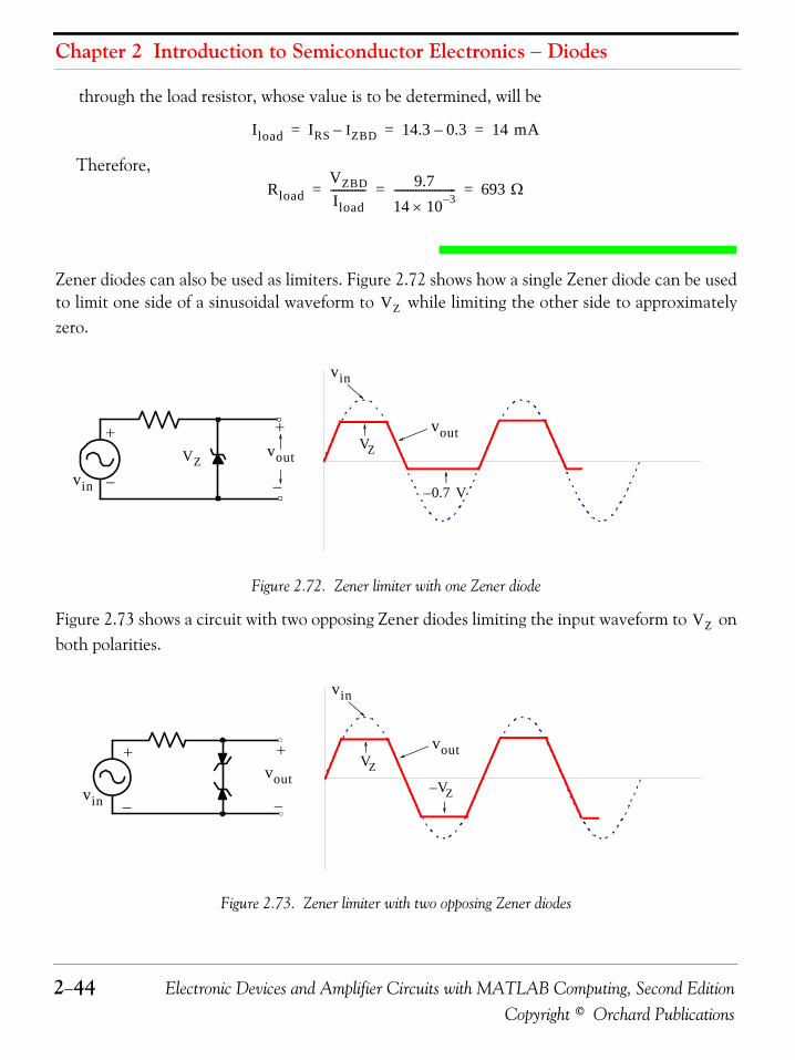
Chapter 2 Introduction to Semiconductor Electronics − Diodes
2−44 Electronic Devices and Amplifier Circuits with MATLAB Computing, Second EditionCopyright © Orchard Publications
through the load resistor, whose value is to be determined, will be
Therefore,
Zener diodes can also be used as limiters. Figure 2.72 shows how a single Zener diode can be usedto limit one side of a sinusoidal waveform to while limiting the other side to approximatelyzero.
Figure 2.72. Zener limiter with one Zener diode
Figure 2.73 shows a circuit with two opposing Zener diodes limiting the input waveform to onboth polarities.
Figure 2.73. Zener limiter with two opposing Zener diodes
Iload IRS IZBD– 14.3 0.3– 14 mA= = =
RloadVZBDIload------------- 9.7
14 10 3–×----------------------- 693 Ω= = =
VZ
+
−
VZ
+
−
vout
vout
vin
VZ
0.7 V–vin
VZ
vout
vin
VZ
VZ–
+
−
+
−
voutvin

Electronic Devices and Amplifier Circuits with MATLAB Computing, Second Edition 2−45Copyright © Orchard Publications
The Schottky Diode
2.14 The Schottky Diode
A Schottky diode is a junction of a lightly doped −type semiconductor with a metal electrode asshown in Figure 2.74(a). Figure 2.74(b) shows the Schottky diode symbol.
Figure 2.74. The components of a Schottky diode and its symbol
The junction of a doped semiconductor − usually −type − with a special metal electrode can pro-duce a very fast switching diode which is mainly used in high (up to 5 MHz) frequency circuits orhigh speed digital circuits. When the diode is forward−biased, the electrons move from the −typematerial to the metal and give up their energy quickly. Since there are no minority carriers (holes)the conduction stops quickly and changes to reverse−bias.
Schottky diodes find wide application as rectifiers for high frequency signals and also are used inthe design of galliun arsenide circuits. The forward voltage drop of a conducting Schottky diode istypically 0.3 to 0.5 volt compared to the 0.6 to 0.8 found in silicon junction diodes.
2.15 The Tunnel Diode
The conventional junction diode uses semiconductor materials that are lightly doped with oneimpurity atom for ten−million semiconductor atoms. This low doping level results in a relativelywide depletion region. Conduction occurs in the normal junction diode only if the voltage appliedto it is large enough to overcome the potential barrier of the junction. In 1958, Leo Esaki, a Japa-nese scientist, discovered that if a semiconductor junction diode is heavily doped with impurities,it will have a region of negative resistance. This type of diode is known as tunnel diode.
In a tunnel diode the semiconductor materials used in forming a junction are doped to the extentof one−thousand impurity atoms for ten−million semiconductor atoms. This heavy doping pro-duces an extremely narrow depletion zone similar to that in the Zener diode. Also because of theheavy doping, a tunnel diode exhibits an unusual current−voltage characteristic curve as com-pared with that of an ordinary junction diode. The characteristic curve for a tunnel diode and itssymbol are shown in Figure 2.75.
From Figure 2.75 we see that the current increases to a peak value with a small applied forwardbias voltage (point 1 to 2), then the current decreases with an increasing forward bias to a mini-mum current (point 2 to 3), and it starts increasing again with further increases in the bias voltagepoint 3 to 4.)
n
n type–materialelectrode
metal
a( ) b( )
n
n
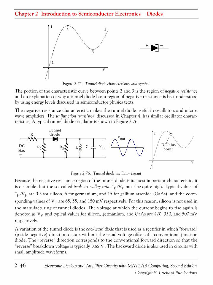
Chapter 2 Introduction to Semiconductor Electronics − Diodes
2−46 Electronic Devices and Amplifier Circuits with MATLAB Computing, Second EditionCopyright © Orchard Publications
Figure 2.75. Tunnel diode characteristics and symbol
The portion of the characteristic curve between points 2 and 3 is the region of negative resistanceand an explanation of why a tunnel diode has a region of negative resistance is best understoodby using energy levels discussed in semiconductor physics texts.
The negative resistance characteristic makes the tunnel diode useful in oscillators and micro-wave amplifiers. The unijunction transistor, discussed in Chapter 4, has similar oscillator charac-teristics. A typical tunnel diode oscillator is shown in Figure 2.76.
Figure 2.76. Tunnel diode oscillator circuit
Because the negative resistance region of the tunnel diode is its most important characteristic, itis desirable that the so−called peak−to−valley ratio must be quite high. Typical values of
are 3.5 for silicon, 6 for germanium, and 15 for gallium arsenide (GaAs), and the corre-sponding values of are 65, 55, and 150 mV respectively. For this reason, silicon is not used inthe manufacturing of tunnel diodes. The voltage at which the current begins to rise again isdenoted as and typical values for silicon, germanium, and GaAs are 420, 350, and 500 mVrespectively.
A variation of the tunnel diode is the backward diode that is used as a rectifier in which “forward”(p side negative) direction occurs without the usual voltage offset of a conventional junctiondiode. The “reverse” direction corresponds to the conventional forward direction so that the“reverse” breakdown voltage is typically . The backward diode is also used in circuits withsmall amplitude waveforms.
4
3
1
2i
v
vout
vout
+
−
DCbias
R1
R2 R3 L C+
−
Tunneldiode
DC biaspoint
v
i
IP VP⁄
IP VP⁄
VP
VV
0.65 V

Electronic Devices and Amplifier Circuits with MATLAB Computing, Second Edition 2−47Copyright © Orchard Publications
The Tunnel Diode
Example 2.12
A DC voltage source, a tunnel diode whose characteristics are as shown, and a resistor areconnected in series as shown in Figure 2.77. Find the current
Figure 2.77. Circuit and tunnel diode characteristics for Example 2.12
Solution:
Let the voltage across the tunnel diode be and the voltage across the resistor be . Then,
or(2.35)
When , (2.35) reduces to and when , , and withthese values we draw the load line shown in Figure 2.78. We observe that when ,
, when , , and when , .
Figure 2.78. Graphical solution for the determination of the current for the circuit of Figure 2.77
i v–
i
i mA( )
v V( )0.1 0.2 0.3 0.4 0.5 0.6
40
30
20
0
10
0.7
0.6 V 20 Ω
i
i v–
VTD VR
VTD VR+ 0.6 V=
VTD 20i+ 0.6 V=
i 0= VTD 0.6= VTD 0= i 0.6 20⁄ 30 mA= =
VTD 0.11 V≈
i 25 mA≈ VTD 0.29 V≈ i 16 mA≈ VTD 0.52 V≈ i 4 mA≈
i mA( )
v V( )0.1 0.2 0.3 0.4 0.5 0.6
30
20
0
10
0.7
i

Chapter 2 Introduction to Semiconductor Electronics − Diodes
2−48 Electronic Devices and Amplifier Circuits with MATLAB Computing, Second EditionCopyright © Orchard Publications
2.16 The VaractorThe varactor, or varicap, is a diode that behaves like a variable capacitor, with the PN junctionfunctioning like the dielectric and plates of a common capacitor. For this reason, the symbol for avaractor is as shown in Figure 2.79.
Figure 2.79. Symbol for varactor
A varactor diode uses a PN junction in reverse bias and has a structure such that the capacitanceof the diode varies with the reverse voltage. A voltage controlled capacitance is useful in tuningapplications. Typical capacitance values are small, in the order of picofarads.
Presently, varactors are replacing the old variable capacitor tuning circuits as in television tuners.Figure 2.80 shows a typical varactor tuning circuit where the DC control voltage changes thecapacitance of the varactor to form a resonant circuit.
Figure 2.80. A varactor tuner circuit
2.17 Optoelectronic DevicesOptoelectronic devices either produce light or use light in their operation. The first of these, thelight−emitting diode (LED), was developed to replace the fragile, short−life incandescent lightbulbs used to indicate on/off conditions on instrument panels. A light−emitting diode, when for-ward biased, produces visible light. The light may be red, green, or amber, depending upon thematerial used to make the diode.
The circuit symbols for all optoelectronic devices have arrows pointing either toward them, ifthey use light, or away from them, if they produce light. The LED is designated by a standarddiode symbol with two arrows pointing away from the cathode as shown in Figure 2.81 where thearrows indicate light leaving the diode.
Figure 2.81. Symbol for LED
VC
VC
R
vin
+
−
−
+
L vout

Electronic Devices and Amplifier Circuits with MATLAB Computing, Second Edition 2−49Copyright © Orchard Publications
Optoelectronic Devices
The LED operating voltage is small, about 1.6 volts forward bias and generally about 10 milliam-peres. The life expectancy of the LED is very long, over 100,000 hours of operation. For this rea-son, LEDs are used widely as “power on” indicators of digital voltmeters, frequency counters, etc.and as displays for pocket calculators where they form seven−segment displays, as shown in Figure2.82.
Figure 2.82. LEDs arranged for seven segment display
In Figure 2.82 the anodes are internally connected. When a negative voltage is applied to theproper cathodes, a number is formed. For example, if negative voltage is applied to all cathodesthe number 8 is produced, and if a negative voltage is changed and applied to all cathodes exceptLED and the number 5 is displayed.
Seven−segment displays are also available in common−cathode form, in which all cathodes are atthe same potential. When replacing LED displays, one must ensure the replacement display is thesame type as the faulty display. Since both types look alike, the manufacturer’s number should bechecked.
Laser diodes are LEDs specifically designed to produce coherent light with a narrow bandwidth andare suitable for CD players and optical communications.
Another optoelectronic device in common use today is the photodiode. Unlike the LED, whichproduces light, the photodiode receives light and converts it to electrical signals. Basically, thephotodiode is a light−controlled variable resistor. In total darkness, it has a relatively high resis-tance and therefore conducts little current. However, when the PN junction is exposed to anexternal light source, internal resistance decreases and current flow increases. The photodiode isoperated with reverse−bias and conducts current in direct proportion to the intensity of the light
a
b
c
d
e
f
g
b e

Chapter 2 Introduction to Semiconductor Electronics − Diodes
2−50 Electronic Devices and Amplifier Circuits with MATLAB Computing, Second EditionCopyright © Orchard Publications
source. The symbol for a photodiode is shown in Figure 2.83 where the arrows pointing towardthe diode indicate that light is required for operation of the device.
Figure 2.83. Symbol for photodiode
Switching the light source on or off changes the conduction level of the photodiode and varyingthe light intensity controls the amount of conduction. Photodiodes respond quickly to changes inlight intensity, and for this reason are extremely useful in digital applications such as photo-graphic light meters and optical scanning equipment.
A phototransistor is another optoelectronic device that conducts current when exposed to light.We will discuss phototransistor in the next chapter.
An older device that uses light in a way similar to the photodiode is the photoconductive cell, orphotocell, shown with its schematic symbol in Figure 2.84. Like the photodiode, the photocell is alight−controlled variable resistor. However, a typical light−to−dark resistance ratio for a photo-cell is 1: 1000. This means that its resistance could range from 1000 ohms in the light to 1000kilohms in the dark, or from 2000 ohms in the light to 2000 kilohms in the dark, and so forth. Ofcourse, other ratios are also available. Photocells are used in various types of control and timingcircuits as, for example, the automatic street light controllers in most cities. The symbol for aphotocell is shown in Figure 2.84.
Figure 2.84. Symbol for photocell
A solar cell is another device that converts light energy into electrical energy. A solar cell actsmuch like a battery when exposed to light and produces about volt across its terminals,with current capacity determined by its size. As with batteries, solar cells may be connected inseries or parallel to produce higher voltages and currents. The device is finding widespread appli-cation in communications satellites and solar−powered homes. The symbol for a solar cell isshown in Figure 2.85.
Figure 2.85. Symbol for solar cell
0.45 V

Electronic Devices and Amplifier Circuits with MATLAB Computing, Second Edition 2−51Copyright © Orchard Publications
Optoelectronic Devices
Figure 2.86 shows an optical coupler, also referred to as an optoisolator. The latter name is derivedfrom the fact that it provides isolation between the input and output. It consists of an LED and aphotodiode and each of these devices are isolated from each other.
Figure 2.86. An optical coupler
Isolation between the input and output is desirable because it reduces electromagnetic interfer-ence. Their most important application is in fiber optic communications links.
PhotodiodeLED

Chapter 2 Introduction to Semiconductor Electronics − Diodes
2−52 Electronic Devices and Amplifier Circuits with MATLAB Computing, Second EditionCopyright © Orchard Publications
2.18 Summary• In a crystal of pure silicon that has been thermally agitated there is an equal number of free
electrons and holes. A free electron is one which has escaped from its valence orbit and thevacancy it has created is called a hole.
• Doping is a process where impurity atoms which are atoms with five valence electrons such asphosphorous, arsenic, and antimony, or atoms with three valence electrons such as boron,aluminum, and gallium, are added to melted silicon.
• An N−type semiconductor has more free electrons than holes and for this reason the freeelectrons are considered to be the majority carriers and the holes the minority carriers.
• A P−type semiconductor has more holes than free electrons and thus the holes are the major-ity carriers and the free electrons are the minority carriers.
• A junction diode is formed when a piece of P−type material and a piece of N−type material arejoined together. The area between the P−type and N−type materials is referred to as thedepletion region.
• The electrostatic field created by the positive and negative ions in the depletion region iscalled a barrier.
• A forward−biased PN junction is formed if we attach a voltage source to a junction diode withthe plus (+) side of the voltage source connected to the P−type material and the minus (−)side to the N−type. When a junction diode is forward−biased, conventional current will flowin the direction of the arrow on the diode symbol.
• A reverse−biased PN junction is formed if we attach a voltage source to a junction diode withthe plus (+) side of the voltage source connected to the N−type material and the minus (−)side to the P−type.
• The P−type side of the junction diode is also referred to as the anode and the N−type side asthe cathode.
• The relationship in a forward−biased junction diode is the nonlinear relation
where is the current through the diode, is the voltage drop across the diode, is thereverse current, that is, the current which would flow through the diode if the polarity of
is reversed, is charge of an electron, that is, , the coefficient var-ies from 1 to 2 depending on the current level and the nature or the recombination near the
junction, , that is, , and is the
absolute temperature in degrees Kelvin, that is, . It is conve-
iD vD–
iD Ir e qvD nkT⁄( ) 1–[ ]=
iD vD Ir
vD
q q 1.6 10 19– coulomb×= n
k Boltzmann's constant= k 1.38 10 23– × joule Kelvin⁄= T
T 273 temperature in Co+=
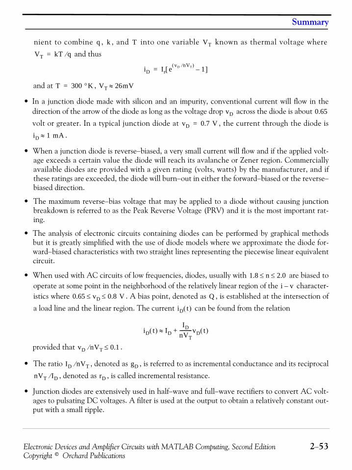
Electronic Devices and Amplifier Circuits with MATLAB Computing, Second Edition 2−53Copyright © Orchard Publications
Summary
nient to combine , , and into one variable known as thermal voltage where and thus
and at ,
• In a junction diode made with silicon and an impurity, conventional current will flow in thedirection of the arrow of the diode as long as the voltage drop across the diode is about volt or greater. In a typical junction diode at , the current through the diode is
.
• When a junction diode is reverse−biased, a very small current will flow and if the applied volt-age exceeds a certain value the diode will reach its avalanche or Zener region. Commerciallyavailable diodes are provided with a given rating (volts, watts) by the manufacturer, and ifthese ratings are exceeded, the diode will burn−out in either the forward−biased or the reverse−biased direction.
• The maximum reverse−bias voltage that may be applied to a diode without causing junctionbreakdown is referred to as the Peak Reverse Voltage (PRV) and it is the most important rat-ing.
• The analysis of electronic circuits containing diodes can be performed by graphical methodsbut it is greatly simplified with the use of diode models where we approximate the diode for-ward−biased characteristics with two straight lines representing the piecewise linear equivalentcircuit.
• When used with AC circuits of low frequencies, diodes, usually with are biased tooperate at some point in the neighborhood of the relatively linear region of the character-istics where . A bias point, denoted as , is established at the intersection ofa load line and the linear region. The current can be found from the relation
provided that .
• The ratio , denoted as , is referred to as incremental conductance and its reciprocal, denoted as , is called incremental resistance.
• Junction diodes are extensively used in half−wave and full−wave rectifiers to convert AC volt-ages to pulsating DC voltages. A filter is used at the output to obtain a relatively constant out-put with a small ripple.
q k T VT
VT kT q⁄=
iD Ir e vD nVT⁄( ) 1–[ ]=
T 300 °K= VT 26mV≈
vD 0.65
vD 0.7 V=
iD 1 mA≈
1.8 n 2.0≤ ≤i v–
0.65 vD 0.8 V≤ ≤ Q
iD t( )
iD t( ) IDID
nVT----------vD t( )+≈
vD nVT⁄ 0.1≤
ID nVT⁄ gD
nVT ID⁄ rD
Chapter 2 Introduction to Semiconductor Electronics − Diodes
2−54 Electronic Devices and Amplifier Circuits with MATLAB Computing, Second EditionCopyright © Orchard Publications
• A peak rectifier circuit is a simple series circuit with a capacitor, a diode, and an AC voltagesource where the output voltage across the capacitor is approximately equal to the peak valueof the input AC voltage. If a resistor is placed in parallel with the capacitor and theirvalues are chosen such that the time constant is much greater than the dischargeinterval, the peak rectifier circuit will behave like an AC to DC converter.
• Clipper (or limiter) circuits consist of diodes, resistors, and sometimes DC sources to clip orlimit the output to a certain level. Clipper circuits are used in applications where it is neces-sary to limit the input to another circuit so that the latter would not be damaged.
• A DC restorer (or clamped capacitor) is a circuit that can restore a DC voltage to a desiredDC level. In its basic form is a series circuit with a voltage source, a capacitor, and a diode,and the output is the voltage across the diode.
• A voltage doubler circuit is a combination of a DC restorer and a peak rectifier. Voltage tri-plers and voltage quadruplers are also possible with additional diodes and capacitors.
• Zener diodes are designed to operate in the reverse voltage breakdown (avalanche) region. AZener diode is always connected as a reverse−biased diode and its voltage rating and themaximum power it can absorb are given by the manufacturer. Their most important applica-tion is in voltage regulation.
• Zener diodes can also be used as limiters and limiting can occur during the positive half−cycleof the input voltage, during the negative half−cycle, or during both the positive and negativehalf−cycles of the input voltage.
• A Schottky diode is a junction of a lightly doped −type semiconductor with a metal elec-trode. The junction of a doped semiconductor − usually −type − with a special metal elec-trode can produce a very fast switching diode which is mainly used in high (up to 5 MHz) fre-quency circuits or high speed digital circuits. Schottky diodes find wide application asrectifiers for high frequency signals and also are used in the design of galliun arsenide (GaAs)circuits. The forward voltage drop of a conducting Schottky diode is typically 0.3 to 0.5 voltcompared to the 0.6 to 0.8 found in silicon junction diodes.
• A tunnel diode is one which is heavily doped with impurities, it will have a region of negativeresistance. The negative resistance characteristic makes the tunnel diode useful in oscillatorsand microwave amplifiers.
• The backward diode is a variation of the tunnel diode. It is used as a rectifier and in circuitswith small amplitude waveforms.
• A varactor, or varicap, is a diode that behaves like a variable capacitor, with the PN junctionfunctioning like the dielectric and plates of a common capacitor. A varactor diode uses a PNjunction in reverse bias and has a structure such that the capacitance of the diode varies withthe reverse voltage. A voltage controlled capacitance is useful in tuning applications. Typical
R Cτ RC=
VZ
nn
Electronic Devices and Amplifier Circuits with MATLAB Computing, Second Edition 2−55Copyright © Orchard Publications
Summary
capacitance values are small, in the order of picofarads. Varactors have now replaced the oldvariable capacitor tuning circuits as in television tuners.
• Optoelectronic devices either produce light or use light in their operation.
• A Light−Emitting Diode (LED) is an optoelectronic device that, when forward biased, pro-duces visible light. The light may be red, green, or amber, depending upon the material used tomake the diode. The life expectancy of the LED is very long, over 100,000 hours of operation.For this reason, LEDs are used widely as “power on” indicators of digital voltmeters, frequencycounters, etc. and as displays for pocket calculators where they form seven−segment displays.
• Laser diodes are LEDs specifically designed to produce coherent light with a narrow bandwidthand are suitable for CD players and optical communications.
• A photodiode is another optoelectronic device which receives light and converts it to electricalsignals. Photodiodes respond quickly to changes in light intensity, and for this reason areextremely useful in digital applications such as photographic light meters and optical scanningequipment.
• A photocell is an older device that uses light in a way similar to the photodiode. Photocells areused in various types of control and timing circuits as, for example, the automatic street lightcontrollers in most cities.
• A solar cell is another device that converts light energy into electrical energy. A solar cell actsmuch like a battery when exposed to light and as with batteries, solar cells may be connected inseries or parallel to produce higher voltages and currents. Solar cells find widespread applica-tion in communications satellites and solar−powered homes.
• An optical coupler, sometimes referred to as an optoisolator, consists of an LED and a photo-diode and each of these devices are isolated from each other. Isolation between the input andoutput is desirable because it reduces electromagnetic interference. Their most importantapplication is in fiber optic communications links.
Chapter 2 Introduction to Semiconductor Electronics − Diodes
2−56 Electronic Devices and Amplifier Circuits with MATLAB Computing, Second EditionCopyright © Orchard Publications
2.19 Exercises
1. Plot the characteristics of a forward−biased junction diode with at .
2. Show that for a decade (factor 10) change in current of a forward−biased junction diodethe voltage changes by a factor of . Hint: Start with the approximate relation
, form the ratio corresponding to the ratio , and plot in semi-log scale.
3. Suggest an experiment that will enable one to compute the numerical value of .
4. It is known that for a certain diode at . and the reverse current increases by about per rise. At what temperature will double in value? Whatconclusion can we draw from the result?
5. When a junction diode operates at the reverse−bias region and before avalanche occurs,the current is almost constant. Assuming that we can show that and for
this reason is often referred to as the saturation current and whereas in the forward−biased
region has a typical value of to at , a typical value in the reverse−
biased region is . Also, the reverse current doubles for every rise in temperature.
In the circuit below, the applied voltage is not sufficient to drive the diode into the ava-lanche region, and it is known that at .
Find:
a. at
b. at
6. For the circuit below, find the value of assuming that all three diodes are ideal. Compareyour answer with that of Example 2.4. Make any reasonable assumptions.
i v– n 2= 27 °C
iD
vD 2.3nVT
iD IrevD nVT⁄
≈ VD2 VD1⁄ ID2 ID1⁄
n
Ir 10 13– A= 50 °C Ir
15% 1 °C Ir
v 0<Ir v VT» iD Ir–≈
Ir
Ir 10 14– A 10 15– A 27 °C
10 9– A 10 °C
VS
VR 0.5 V= 20 °C
KΩVR
Ir
VS 500
VR 0 °C
VR 40 °C
Vout
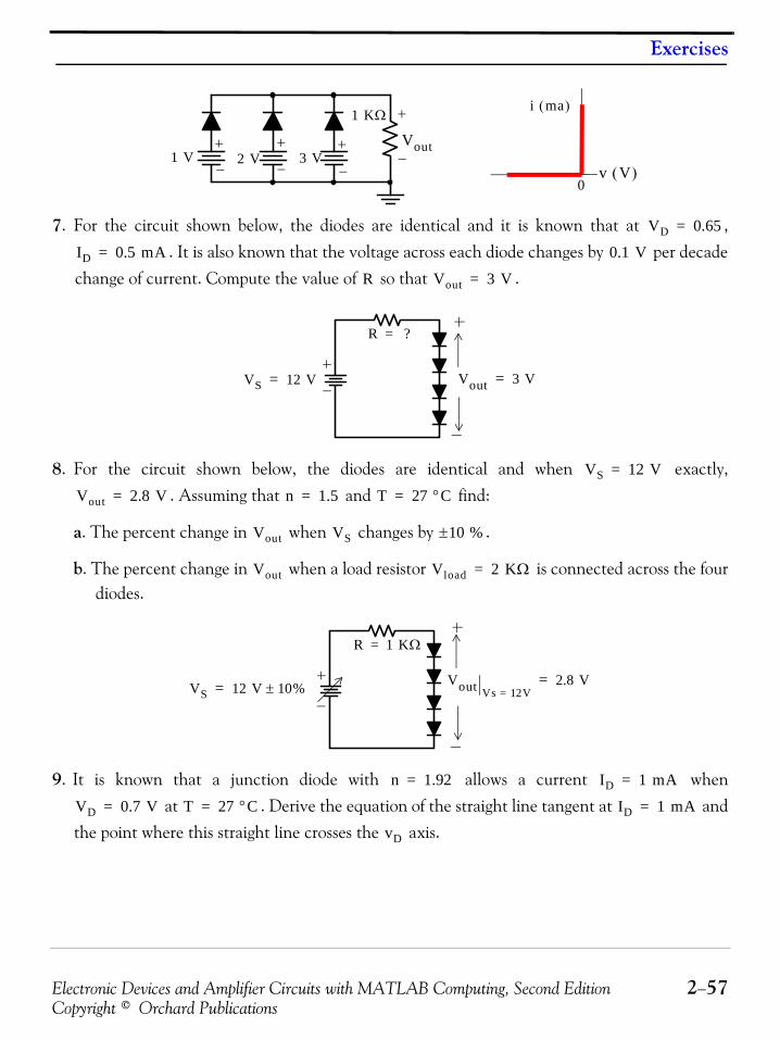
Electronic Devices and Amplifier Circuits with MATLAB Computing, Second Edition 2−57Copyright © Orchard Publications
Exercises
7. For the circuit shown below, the diodes are identical and it is known that at ,. It is also known that the voltage across each diode changes by per decade
change of current. Compute the value of so that .
8. For the circuit shown below, the diodes are identical and when exactly,. Assuming that and find:
a. The percent change in when changes by .
b. The percent change in when a load resistor is connected across the fourdiodes.
9. It is known that a junction diode with allows a current when at . Derive the equation of the straight line tangent at and
the point where this straight line crosses the axis.
1 V
1 KΩ
Vout2 V 3 V
v V( )
i ma( )
0
VD 0.65=
ID 0.5 mA= 0.1 V
R Vout 3 V=
VS 12 V=
R ?=
Vout 3 V=
VS 12 V=
Vout 2.8 V= n 1.5= T 27 °C=
Vout VS 10 %±
Vout Vload 2 KΩ=
VS 12 V 10%±=
R 1 KΩ=
Vout Vs 12V=2.8 V=
n 1.92= ID 1 mA=
VD 0.7 V= T 27 °C= ID 1 mA=
vD
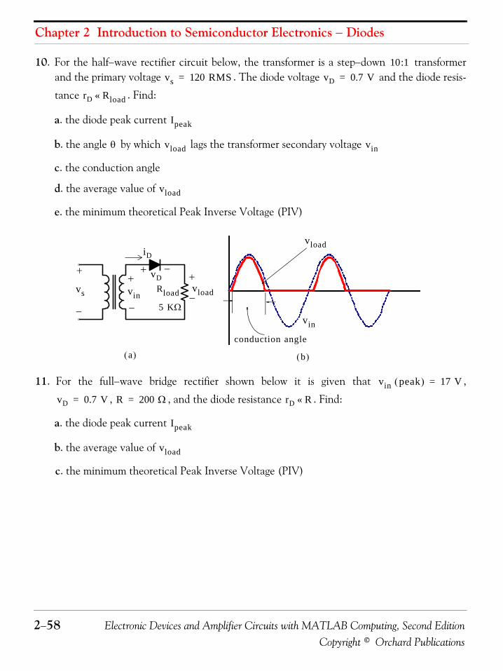
Chapter 2 Introduction to Semiconductor Electronics − Diodes
2−58 Electronic Devices and Amplifier Circuits with MATLAB Computing, Second EditionCopyright © Orchard Publications
10. For the half−wave rectifier circuit below, the transformer is a step−down transformerand the primary voltage . The diode voltage and the diode resis-
tance . Find:
a. the diode peak current
b. the angle by which lags the transformer secondary voltage
c. the conduction angle
d. the average value of
e. the minimum theoretical Peak Inverse Voltage (PIV)
11. For the full−wave bridge rectifier shown below it is given that ,
, , and the diode resistance . Find:
a. the diode peak current
b. the average value of
c. the minimum theoretical Peak Inverse Voltage (PIV)
10:1vs 120 RMS= vD 0.7 V=
rD Rload«
Ipeak
θ vload vin
vload
vload
b( )
conduction angle
+
vs
−
+
−
iD
+ −vDRload
5 KΩ
a( )
+
−vload
vin
vin
vin peak( ) 17 V=
vD 0.7 V= R 200 Ω= rD R«
Ipeak
vload
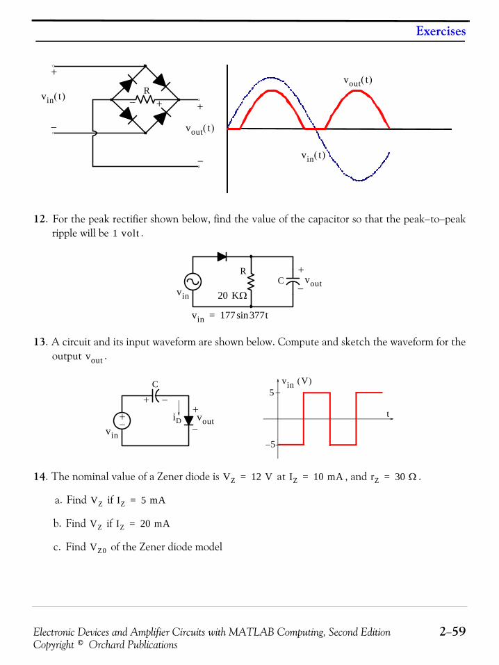
Electronic Devices and Amplifier Circuits with MATLAB Computing, Second Edition 2−59Copyright © Orchard Publications
Exercises
12. For the peak rectifier shown below, find the value of the capacitor so that the peak−to−peakripple will be .
13. A circuit and its input waveform are shown below. Compute and sketch the waveform for theoutput .
14. The nominal value of a Zener diode is at , and .
a. Find if
b. Find if
c. Find of the Zener diode model
vin t( )
vout t( )
vin t( )
+
−
R+−
vout t( )
+
−
1 volt
+
−vout
R
20 KΩ
vin 177 377tsin=
Cvin
vout
t
vin V( )
5–
5
+−
C
+ −
iD+
−vout
vin
VZ 12 V= IZ 10 mA= rZ 30 Ω=
VZ IZ 5 mA=
VZ IZ 20 mA=
VZ0
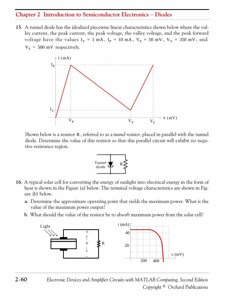
Chapter 2 Introduction to Semiconductor Electronics − Diodes
2−60 Electronic Devices and Amplifier Circuits with MATLAB Computing, Second EditionCopyright © Orchard Publications
15. A tunnel diode has the idealized piecewise linear characteristics shown below where the val-ley current, the peak current, the peak voltage, the valley voltage, and the peak forwardvoltage have the values , , , , and
respectively.
Shown below is a resistor , referred to as a tunnel resistor, placed in parallel with the tunneldiode. Determine the value of this resistor so that this parallel circuit will exhibit no nega-tive resistance region.
16. A typical solar cell for converting the energy of sunlight into electrical energy in the form ofheat is shown in the Figure (a) below. The terminal voltage characteristics are shown in Fig-ure (b) below.a. Determine the approximate operating point that yields the maximum power. What is the
value of the maximum power output?b. What should the value of the resistor be to absorb maximum power from the solar cell?
IV 1 mA= IP 10 mA= VP 50 mV= VV 350 mV=
VF 500 mV=
i mA( )
VP
IV
IP
VV VFv mV( )
R
Tunnel Rdiode
Light
v
i (mA)
v (mV)200 400
20
40
R
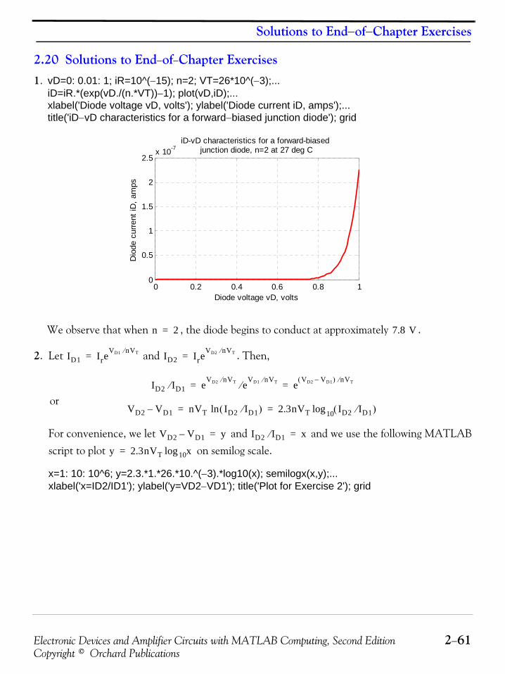
Electronic Devices and Amplifier Circuits with MATLAB Computing, Second Edition 2−61Copyright © Orchard Publications
Solutions to End−of−Chapter Exercises
2.20 Solutions to End−of−Chapter Exercises1. vD=0: 0.01: 1; iR=10^(−15); n=2; VT=26*10^(−3);...
iD=iR.*(exp(vD./(n.*VT))−1); plot(vD,iD);...xlabel('Diode voltage vD, volts'); ylabel('Diode current iD, amps');...title('iD−vD characteristics for a forward−biased junction diode'); grid
We observe that when , the diode begins to conduct at approximately .
2. Let and . Then,
or
For convenience, we let and and we use the following MATLABscript to plot on semilog scale.
x=1: 10: 10^6; y=2.3.*1.*26.*10.^(−3).*log10(x); semilogx(x,y);...xlabel('x=ID2/ID1'); ylabel('y=VD2−VD1'); title('Plot for Exercise 2'); grid
0 0.2 0.4 0.6 0.8 10
0.5
1
1.5
2
2.5x 10
-7
Diode voltage vD, volts
Dio
de c
urre
nt iD
, am
psiD-vD characteristics for a forward-biased
junction diode, n=2 at 27 deg C
n 2= 7.8 V
ID1 IreVD1 nVT⁄
= ID2 IreVD2 nVT⁄
=
ID2 ID1⁄ eVD2 nVT⁄ eVD1 nVT⁄⁄ e VD2 VD1–( ) nVT⁄
= =
VD2 VD1– nVT ID2 ID1⁄( )ln 2.3nVT ID2 ID1⁄( )10log= =
VD2 VD1– y= ID2 ID1⁄ x=
y 2.3nVT x10log=
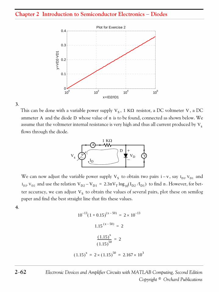
Chapter 2 Introduction to Semiconductor Electronics − Diodes
2−62 Electronic Devices and Amplifier Circuits with MATLAB Computing, Second EditionCopyright © Orchard Publications
3.This can be done with a variable power supply , resistor, a DC voltmeter , a DCammeter and the diode whose value of is to be found, connected as shown below. Weassume that the voltmeter internal resistance is very high and thus all current produced by flows through the diode.
We can now adjust the variable power supply to obtain two pairs , say and and use the relation to find . However, for bet-
ter accuracy, we can adjust to obtain the values of several pairs, plot these on semilogpaper and find the best straight line that fits these values.
4.
100
102
104
106
0
0.1
0.2
0.3
0.4
x=ID2/ID1
y=V
D2-
VD
1
Plot for Exercise 2
VS 1 KΩ V
A D nVs
VVD
DVs
ID
1 KΩA
VS i v– ID1 VD1,
ID2 VD2, VD2 VD1– 2.3nVT ID2 ID1⁄( )10log= n
VS
10 13– 1 0.15+( ) x 50–( ) 2 10 13–×=
1.15 x 50–( ) 2=
1.15( )x
1.15( )50------------------- 2=
1.15( )x 2 1.15( )50× 2.167 103×= =

Electronic Devices and Amplifier Circuits with MATLAB Computing, Second Edition 2−63Copyright © Orchard Publications
Solutions to End−of−Chapter Exercises
Therefore, we can conclude that the reverse current doubles for every rise in tempera-ture.
5.At ,
and since the reverse current doubles for every rise in temperature, we have:
a.
and
b.
and
6. We assume that diode and the resistor are connected first. Then, and stays at
this value because diodes and , after being connected to the circuit, are reverse−biased.
The value of is unrealistic when compared with the realistic value which we foundin Example 2.4. This is because we’ve assumed ideal diodes, a physical impossibility.
1.15( )x10log x 1.15( )10log 2.167 103×( )10log= =
x 1.15( )10log 2.167( )10log 3 10( )10log+ 0.336 3+ 3.336= = =
x 3.336 1.1510log⁄ 54.96 °C= = 55 °C≈
Ir 5 °C
20 °C
Ir 20 °C
0.5 V500 KΩ-------------------- 1 μA= =
10 °C
Ir 40 °C2 2 1 μA×× 4 μA= =
VR 40 °C4 10 6–× 500 103×× 2V= =
Ir 0 °C0.5 0.5 1 μA×× 0.25 μA= =
VR 0 °C0.25 10 6–× 500 103×× 0.125 V= =
D3 Vout 3 V=
D1 D2
1 V
1 KΩ
Vout
2 V 3 V v V( )
i ma( )
0
D1 D2 D3
Vout 3 V=
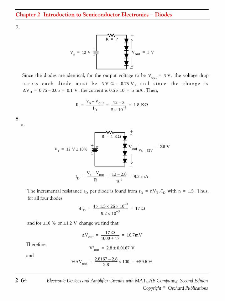
Chapter 2 Introduction to Semiconductor Electronics − Diodes
2−64 Electronic Devices and Amplifier Circuits with MATLAB Computing, Second EditionCopyright © Orchard Publications
7.
Since the diodes are identical, for the output voltage to be , the voltage drop
a c r o s s e a c h d i od e m u s t b e , a n d s i n c e t he c h a n g e i s, the current is . Then,
8.a.
The incremental resistance per diode is found from with . Thus,for all four diodes
and for or change we find that
Therefore,
and
Vs 12 V=
R ?=
Vout 3 V=
Vout 3 V=
3 V 4⁄ 0.75 V=
ΔVD 0.75 0.65– 0.1 V= = 0.5 10× 5 mA=
RVs Vout–
ID----------------------- 12 3–
5 10 3–×-------------------- 1.8 KΩ= = =
Vs 12 V 10%±=
R 1 KΩ=
Vout Vs 12V=2.8 V=
IDVs Vout–
R----------------------- 12 2.8–
103------------------- 9.2 mA= = =
rD rD nVT ID⁄= n 1.5=
4rD4 1.5× 26 10 3–××
9.2 10 3–×---------------------------------------------- 17 Ω= =
10 %± 1.2 V±
ΔVout17 Ω
1000 17+------------------------ 16.7mV= =
V'out 2.8 0.0167 V±=
%ΔVout2.8167 2.8–
2.8------------------------------ 100× 59.6 %±= =

Electronic Devices and Amplifier Circuits with MATLAB Computing, Second Edition 2−65Copyright © Orchard Publications
Solutions to End−of−Chapter Exercises
b.The load when connected across the four diodes will have a voltage of andthus the current through this load will be
Therefore, the current through the four diodes decreases by and the decrease involtage across all four diodes will be
9.
From analytic geometry, the equation of a straight line in an plane is where is the slope and is the intercept. For this exercise the equation of the straight line is
(1)where
and by substitution into (1) above (2)
Next, we find the intercept using the given data that when , . Then,by substitution into (2) we obtain
from which and thus the equation of the straight line becomes
(3)
Now, from (3) above we find that the axis intercept is or .
2 KΩ 2.8 V
Iload2.8 V2 KΩ-------------- 1.4 mA= =
1.4 mA
ΔVout 1.4 mA 17 Ω×– 23.8 mV–= =
iD mA( )
vD V( )
0.7
1
x y– y mx b+=
m b y
iD mvD b+=
m 1rD-----
IDnVT---------- 10 3–
1.92 26 10 3–××---------------------------------------= = 0.02= =
iD 0.02vD b+=
iD vD 0.7 V= iD 1 mA=
10 3– 0.02 0.7× b+=
b 0.013–=
iD 0.02vD 0.013–=
vD 0 0.02vD 0.013–= vD 0.65 V=

Chapter 2 Introduction to Semiconductor Electronics − Diodes
2−66 Electronic Devices and Amplifier Circuits with MATLAB Computing, Second EditionCopyright © Orchard Publications
10.
a. It is given that the transformer is a step down type with ratio ; therefore, the secondary
voltage is or . Then,
and since
b.From (2.15), where . Then,
c. The conduction angle is
d.From (2.17)
e.The minimum theoretical Peak Inverse Voltage (PIV) is
but for practical purposes we should choose the value of
vload
b( )
conduction angle
+
vs
−
+
−
iD
+ −vDRload
5 KΩ
a( )
+
−vload
vin
vin
10:1
12 V RMS vin 12 2 peak 17 V peak= =
Ipeakvin vD–
rD Rload+-------------------------=
rD Rload«
Ipeakvin vD–
Rload------------------- 17 0.7–
5 103×------------------- 3.26 mA= = =
θ Δv Vp⁄1–sin= Δv Vp Vout– vD 0.7 V= = =
θ 0.7 17⁄1–sin 2.36°= =
π 2θ– 180° 2 2.36°×– 175.28°= =
Vload ave( )Vpπ
------ Δv2
-------– 17π------ 0.7
2-------– 5.06 V= =≈
PIV Vp 17 V= =
1.7 PIV× 1.7 17× 30 V≈=
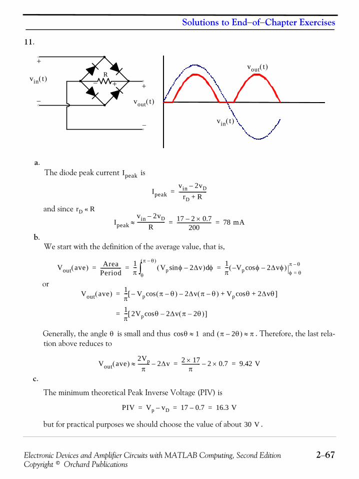
Electronic Devices and Amplifier Circuits with MATLAB Computing, Second Edition 2−67Copyright © Orchard Publications
Solutions to End−of−Chapter Exercises
11.
a.The diode peak current is
and since
b.We start with the definition of the average value, that is,
or
Generally, the angle is small and thus and . Therefore, the last rela-tion above reduces to
c.
The minimum theoretical Peak Inverse Voltage (PIV) is
but for practical purposes we should choose the value of about .
vin t( )
vout t( )
vin t( )
+
−
R+−
vout t( )
+
−
Ipeak
Ipeakvin 2vD–
rD R+-----------------------=
rD R«
Ipeakvin 2vD–
R-----------------------≈ 17 2 0.7×–
200---------------------------- 78 mA= =
Vout ave( ) AreaPeriod----------------- 1
π--- Vp φsin 2Δv–( ) φd
θ
π θ–( )
∫1π--- Vp φcos 2Δvφ––( )
φ θ=
π θ–= = =
Vout ave( ) 1π--- Vp π θ–( )cos 2Δv π θ–( )–– Vp θcos 2Δvθ+ +[ ]=
1π--- 2Vp θcos 2Δv π 2θ–( )–[ ]=
θ θcos 1≈ π 2θ–( ) π≈
Vout ave( )2Vp
π---------- 2Δv–≈ 2 17×
π--------------- 2 0.7×– 9.42 V= =
PIV Vp vD– 17 0.7– 16.3 V= = =
30 V
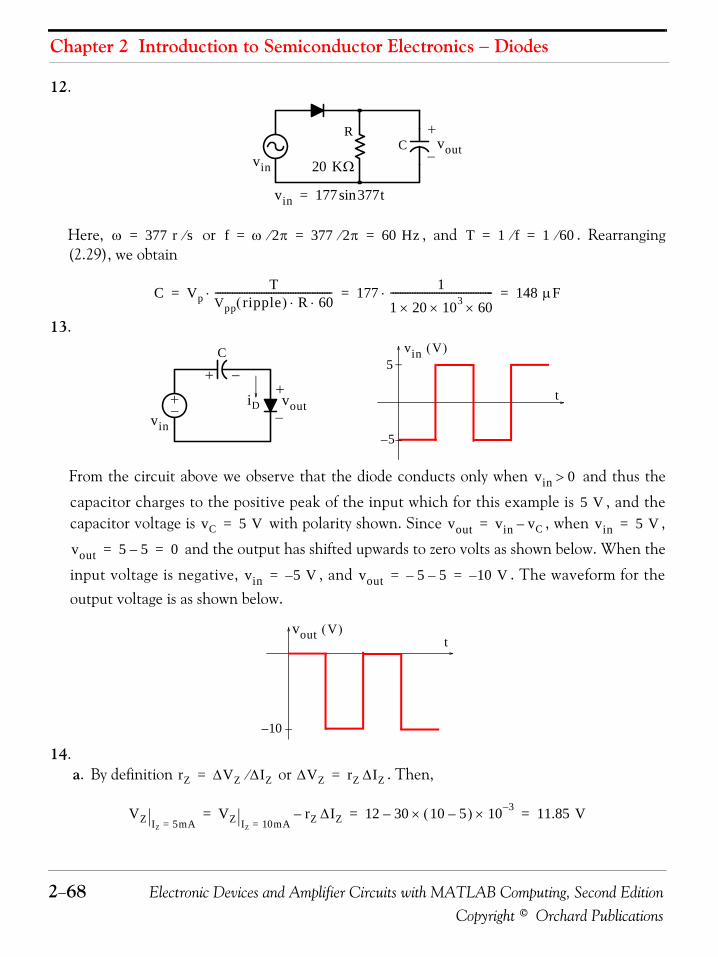
Chapter 2 Introduction to Semiconductor Electronics − Diodes
2−68 Electronic Devices and Amplifier Circuits with MATLAB Computing, Second EditionCopyright © Orchard Publications
12.
Here, or , and . Rearranging(2.29), we obtain
13.
From the circuit above we observe that the diode conducts only when and thus the
capacitor charges to the positive peak of the input which for this example is , and thecapacitor voltage is with polarity shown. Since , when ,
and the output has shifted upwards to zero volts as shown below. When the
input voltage is negative, , and . The waveform for theoutput voltage is as shown below.
14.a. By definition or . Then,
+
−vout
R
20 KΩ
vin 177 377tsin=
Cvin
ω 377 r s⁄= f ω 2π⁄ 377 2π⁄ 60 Hz= = = T 1 f⁄ 1 60⁄= =
C VpT
Vpp ripple( ) R 60⋅ ⋅------------------------------------------------⋅ 177 1
1 20 103×× 60×------------------------------------------⋅ 148 μF= = =
t
vin V( )
5–
5
+−
C
+ −
iD+
−vout
vin
vin 0>
5 VvC 5 V= vout vin vC–= vin 5 V=
vout 5 5– 0= =
vin 5– V= vout 5– 5– 10– V= =
tvout V( )
10–
rZ ΔVZ ΔIZ⁄= ΔVZ rZ ΔIZ=
VZ IZ 5mA=VZ IZ 10mA=
rZ ΔIZ– 12 30 10 5–( ) 10 3–××– 11.85 V= = =

Electronic Devices and Amplifier Circuits with MATLAB Computing, Second Edition 2−69Copyright © Orchard Publications
Solutions to End−of−Chapter Exercises
b.
c. From (2.34) where and are the nominal values. Then
15.
For the region of negative resistance the slope is
and thus
(1)
where and are as shown in the circuit below.
To eliminate the negative resistance region, we must have
VZ IZ 20mA=VZ IZ 10mA=
rZ– ΔIZ 12 30 10 20–( ) 10 3–××– 12.3 V= = =
VZ VZ0 rZIZ+= VZ IZ
VZ0 VZ rZIZ– 12 30 10 10 3–××– 11.7 V= = =
i mA( )
VP
IV
IP
VV VFv mV( )
Tunnel Rdiode
m
m ΔiΔv------- 1 10–
350 50–--------------------- 0.03–= = =
diDdv-------- 0.03 Ω 1––=
iD v
Rvi iD iR

Chapter 2 Introduction to Semiconductor Electronics − Diodes
2−70 Electronic Devices and Amplifier Circuits with MATLAB Computing, Second EditionCopyright © Orchard Publications
(2)
for all values of . Since
it follows that
and (2) above will be satisfied if (3)
From (1) and (3)
and thus the maximum value of the resistor should be . With this value, theslope of the total current versus the voltage across the parallel circuit will be zero. For apositive slope greater than zero we should choose a resistor with a smaller value. Let us plotthe total current versus the voltage with the values and .
We will use the following MATLAB script for the plots.
v=51:0.1:349; m=−0.03; b=11.5; id=m*v+b;...R1=33.33; i1=id+v/R1; R2=25; i2=id+v/R2; plot(v,id,v,i1,v,i2); grid
and upon execution of this script we obtain the plot shown below.
didv------ 0≥
vi iD iR+ iD v R⁄+= =
didv------
diDdv-------- 1
R----+=
1R---- diD
dv--------–≥
1R---- 0.03–( )–≥
R 33.33 Ω≈i v
i v R1 33.33 Ω≈ R2 25 Ω=
50 100 150 200 250 300 3500
5
10
15
v (mV)
i (m
A)
i for R=25 Ohms
i for R=33.33 Ohms
i without resistor

Electronic Devices and Amplifier Circuits with MATLAB Computing, Second Edition 2−71Copyright © Orchard Publications
Solutions to End−of−Chapter Exercises
16.
a. By inspection, the operating point that will yield maximum power is denoted as where
b. The value of that will receive maximum power is
Light
v
i (mA)
v (mV)200 400
20
40
R
Q
Q
Pmax 400 40× 16 mw= =
R
R vi---⎝ ⎠
⎛ ⎞max
40040
--------- 10 Ω= = =

Chapter 2 Introduction to Semiconductor Electronics − Diodes
2−72 Electronic Devices and Amplifier Circuits with MATLAB Computing, Second EditionCopyright © Orchard Publications
NOTES:

Electronic Devices and Amplifier Circuits with MATLAB Computing, Second Edition 3−1Copyright © Orchard Publications
Chapter 3
Bipolar Junction Transistors
his is a long chapter devoted to bipolar junction transistors. The NPN and PNP transistorsare defined and their application as amplifiers is well illustrated with numerous examples.The small and large signal equivalent circuits along with the h−parameter and T−equivalent
circuits are presented, and the Ebers−Moll model is discussed in detail.
3.1 IntroductionTransistors are three terminal devices that can be formed with the combination of two separatePN junction materials into one block as shown in Figure 3.1.
Figure 3.1. NPN and PNP transistor construction and symbols
As shown in Figure 3.1, an NPN transistor is formed with two PN junctions with the P−type mate-rial at the center, whereas a PNP transistor is formed with two PN junctions with the N−typematerial at the center. The three terminals of a transistor, whether it is an NPN or PNP transistor,are identified as the emitter, the base, and the collector. Can a transistor be used just as a diode? Theanswer is yes, and Figure 3.2 shows several possible configurations and most integrated circuitsemploy transistors to operate as diodes.
T
N
NNN
P P
PP
NN P
P PN
E
C
B
EmitterCBE E B C
EmitterBase BaseCollector Collector
E
C
B
NPN Transistor formation and symbol PNP Transistor formation and symbol
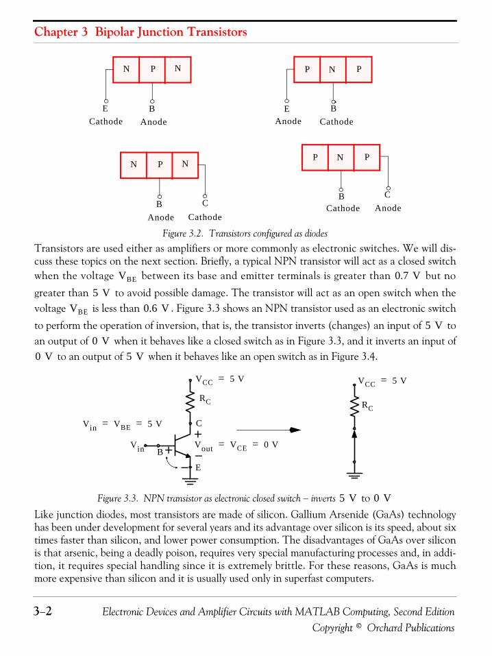
Chapter 3 Bipolar Junction Transistors
3−2 Electronic Devices and Amplifier Circuits with MATLAB Computing, Second EditionCopyright © Orchard Publications
Figure 3.2. Transistors configured as diodes
Transistors are used either as amplifiers or more commonly as electronic switches. We will dis-cuss these topics on the next section. Briefly, a typical NPN transistor will act as a closed switchwhen the voltage between its base and emitter terminals is greater than but no
greater than to avoid possible damage. The transistor will act as an open switch when thevoltage is less than . Figure 3.3 shows an NPN transistor used as an electronic switch
to perform the operation of inversion, that is, the transistor inverts (changes) an input of toan output of when it behaves like a closed switch as in Figure 3.3, and it inverts an input of
to an output of when it behaves like an open switch as in Figure 3.4.
Figure 3.3. NPN transistor as electronic closed switch − inverts to Like junction diodes, most transistors are made of silicon. Gallium Arsenide (GaAs) technologyhas been under development for several years and its advantage over silicon is its speed, about sixtimes faster than silicon, and lower power consumption. The disadvantages of GaAs over siliconis that arsenic, being a deadly poison, requires very special manufacturing processes and, in addi-tion, it requires special handling since it is extremely brittle. For these reasons, GaAs is muchmore expensive than silicon and it is usually used only in superfast computers.
NP PNN P
CathodeBE E B
AnodeAnode Cathode
NN P
CBAnode Cathode
NP P
B CCathode Anode
VBE 0.7 V5 V
VBE 0.6 V5 V
0 V0 V 5 V
E
C
B
VCC 5 V=
RC
Vout VCE 0 V= =
Vin VBE 5 V= =
VCC 5 V=
RC
Vin
5 V 0 V
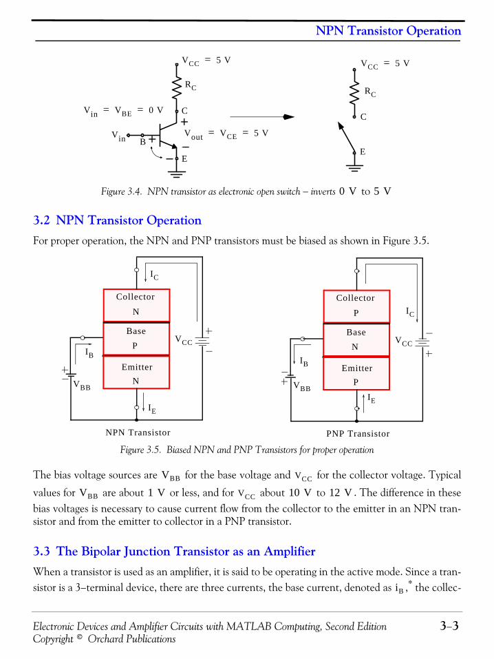
Electronic Devices and Amplifier Circuits with MATLAB Computing, Second Edition 3−3Copyright © Orchard Publications
NPN Transistor Operation
Figure 3.4. NPN transistor as electronic open switch − inverts to
3.2 NPN Transistor OperationFor proper operation, the NPN and PNP transistors must be biased as shown in Figure 3.5.
Figure 3.5. Biased NPN and PNP Transistors for proper operation
The bias voltage sources are for the base voltage and for the collector voltage. Typical
values for are about or less, and for about to . The difference in thesebias voltages is necessary to cause current flow from the collector to the emitter in an NPN tran-sistor and from the emitter to collector in a PNP transistor.
3.3 The Bipolar Junction Transistor as an AmplifierWhen a transistor is used as an amplifier, it is said to be operating in the active mode. Since a tran-sistor is a 3−terminal device, there are three currents, the base current, denoted as ,* the collec-
E
C
B
VCC 5 V=
RC
Vout VCE 5 V= =
Vin VBE 0 V= =
VCC 5 V=
C
E
RC
Vin
0 V 5 V
VCC
VBB
IB
Emitter
Collector
N
N
PBase
IC
IE
NPN Transistor
VCC
VBB
IB Emitter
Collector
P
P
NBase
IC
IE
PNP Transistor
VBB VCC
VBB 1 V VCC 10 V 12 V
iB
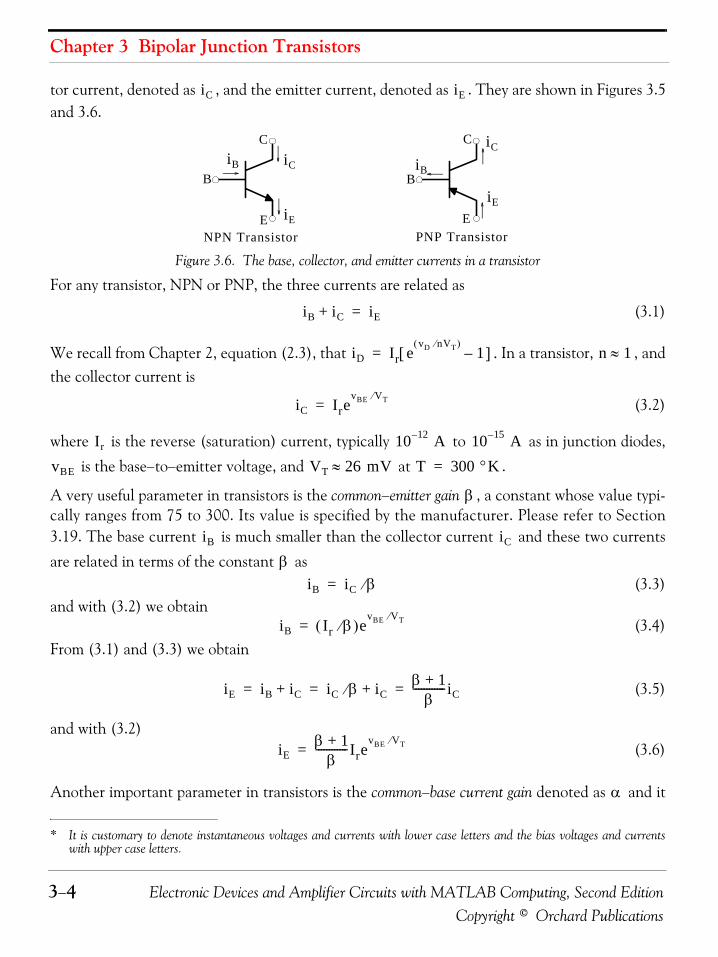
Chapter 3 Bipolar Junction Transistors
3−4 Electronic Devices and Amplifier Circuits with MATLAB Computing, Second EditionCopyright © Orchard Publications
tor current, denoted as , and the emitter current, denoted as . They are shown in Figures 3.5and 3.6.
Figure 3.6. The base, collector, and emitter currents in a transistor
For any transistor, NPN or PNP, the three currents are related as
(3.1)
We recall from Chapter 2, equation (2.3), that . In a transistor, , andthe collector current is
(3.2)
where is the reverse (saturation) current, typically to as in junction diodes,
is the base−to−emitter voltage, and at .
A very useful parameter in transistors is the common−emitter gain , a constant whose value typi-cally ranges from 75 to 300. Its value is specified by the manufacturer. Please refer to Section3.19. The base current is much smaller than the collector current and these two currents
are related in terms of the constant as (3.3)
and with (3.2) we obtain(3.4)
From (3.1) and (3.3) we obtain
(3.5)
and with (3.2)(3.6)
Another important parameter in transistors is the common−base current gain denoted as and it
* It is customary to denote instantaneous voltages and currents with lower case letters and the bias voltages and currentswith upper case letters.
iC iE
E
C
B
E
C
B
NPN Transistor PNP Transistor
iE
iC
iBiB
iE
iC
iB iC+ iE=
iD Ir evD nVT⁄( )
1–[ ]= n 1≈
iC IrevBE VT⁄
=
Ir 10 12– A 10 15– AvBE VT 26 mV≈ T 300 °K=
β
iB iC
βiB iC β⁄=
iB Ir β⁄( )evBE VT⁄
=
iE iB iC+ iC β⁄ iC+β 1+β
------------iC= = =
iEβ 1+β
------------IrevBE VT⁄
=
α

Electronic Devices and Amplifier Circuits with MATLAB Computing, Second Edition 3−5Copyright © Orchard Publications
The Bipolar Junction Transistor as an Amplifier
is related to as
(3.7)
From(3.7) it is obvious that and from (3.5) and (3.7)
(3.8)Also, from (3.6) and (3.7)
(3.9)
and we can express in terms of by rearranging (3.7). Then,
(3.10)
Another lesser known ratio is the common−collector current gain ratio denoted as and it is definedas the ratio of the change in the emitter current to the change in the base current. Thus,
(3.11)
(3.12)
(3.13)
and their relationships are
(3.14)
Example 3.1
A transistor manufacturer produces transistors whose values vary from 0.992 to 0.995. Find the range corresponding to this range.
Solution:
For (3.10) yields
and for ,
β
α ββ 1+------------=
α 1<
iC αiE=
iE1α---Ire
vBE VT⁄=
β α
β α1 α–------------=
γ
αdiC
diE-------=
βdiC
diB-------=
γdiE
diB-------=
α ββ 1+------------= β α
1 α–------------= γ β 1+=
αβ α
α 0.992=
β α1 α–------------ 0.992
1 0.992–---------------------- 124= = =
α 0.995=

Chapter 3 Bipolar Junction Transistors
3−6 Electronic Devices and Amplifier Circuits with MATLAB Computing, Second EditionCopyright © Orchard Publications
Therefore, for the range
the corresponding range is
3.3.1 Equivalent Circuit Models − NPN Transistors
We can draw various equivalent circuit models with dependent voltage and current sources* forNPN transistors using the relations (3.1) through (3.10). To illustrate, let us draw an equivalentcircuit using relations (3.4), (3.3), and (3.1) which are repeated here for convenience.
(3.15)
(3.16)
(3.17)
Figure 3.7. NPN transistor equivalent circuit model for relations (3.15), (3.16), and (3.17)
If we know , , , and the operating temperature, we can find the other parameters for thecircuit model in Figure 3.7.
Example 3.2
For a given NPN transistor, , , , and . Find the
numerical values of the parameters shown in Figure 3.7. The collector bias voltage (not
* Dependent sources are discussed in detail in Chapters 1 through 4, Circuit Analysis I with MATLAB Applications, ISBN978−0−9709511−2−0.
β α1 α–------------ 0.995
1 0.995–---------------------- 199= = =
0.992 α 0.995≤ ≤β
124 β 199≤ ≤
iB Ir β⁄( )evBE VT⁄
=
iC βiB=
iE iB iC+ Ir β⁄( )evBE VT⁄
βiB+= =
Ir β⁄( )evBE VT⁄ vBE
iE
iCiB
iC βiB=
C
E
B
Ir β iB
Ir 2 10 14–×= β 200= iB 5 μA= T 27 °C=
VCC

Electronic Devices and Amplifier Circuits with MATLAB Computing, Second Edition 3−7Copyright © Orchard Publications
The Bipolar Junction Transistor as an Amplifier
shown) is .
Solution:
We find from (3.15), i.e.,
Then,
The collector bias voltage is used for proper transistor operation and its value is not requiredfor the above calculations.
3.3.2 Equivalent Circuit Models − PNP TransistorsRelations (3.15), (3.16), and (3.17) apply also to PNP transistor equivalent circuits except that
needs to be replaced by as shown in Figure 3.8.
Figure 3.8. PNP transistor equivalent circuit model for relations (3.15), (3.16), and (3.17)
For easy reference we summarize the current−voltage relationships for both NPN and PNP transis-tors in the active mode in Table 3.1.
10V
Irβ--- 2 10 14–×
200--------------------- 10 16–= =
vBE
iB Ir β⁄( )evBE VT⁄
=
5 10 6–× 10 16– evBE VT⁄
=
evBE VT⁄ 5 10 6–×
10 16–------------------- 5 1010×= =
vBE VT⁄ 5 1010×( )ln=
vBE VT 5ln 10 10ln+( ) 26 10 3– 1.61 23.03+( )× 0.64 V≈= =
VCC
vBE vEB
Ir β⁄( )evEB VT⁄ vEB
iE
iCiB
iC βiB=
CB
E

Chapter 3 Bipolar Junction Transistors
3−8 Electronic Devices and Amplifier Circuits with MATLAB Computing, Second EditionCopyright © Orchard Publications
The relations in Table 3.1 are very useful in establishing voltage and current levels at variouspoints on an NPN or PNP transistor.
Example 3.3
An NPN transistor with is to operate in the common (grounded) base configuration. ADC power supply at is available and with two external resistors, one connected
between the collector and and the other between the emitter and , we want to keep
the collector current * at and the collector voltage at . Find the values of the
resistors given that when , . The circuit operates at .
Solution:Since the transistor is to operate at the common base configuration, after connecting the resistorsand the bias voltages, our circuit is as shown in Figure 3.9.
Figure 3.9. Transistor circuit for Example 3.3 − Computations for
TABLE 3.1 NPN and PNP transistor current−voltage characteristicsNPN Transistor PNP Transistor
* As stated earlier, we use upper case letters for DC (constant) values, and lower case letters for instantaneous values.
α ββ 1+------------
iCiE-----= = β α
1 α–------------
iCiB-----= =
iE iB iC+=α β
β 1+------------
iCiE-----= = β α
1 α–------------
iCiB-----= =
iE iB iC+=
iBIrβ---⎝ ⎠
⎛ ⎞ e
vBEVT---------
= iC Ire
vBEVT---------
= iEIrα---⎝ ⎠
⎛ ⎞ e
vBEVT---------
= iBIrβ---⎝ ⎠
⎛ ⎞ e
vEBVT---------
= iC Ire
vEBVT---------
= iEIrα---⎝ ⎠
⎛ ⎞ e
vEBVT---------
=
iB iC β⁄= iC βiB= iB iC α⁄= iB iC β⁄= iC βiB= iB iC α⁄=
iB iE β 1+( )⁄= iC αiE= iE β 1+( )iB= iB iE β 1+( )⁄= iC αiE= iE β 1+( )iB=
iB 1 α–( ) iE= VT 26 mV at T 27 °C= = iB 1 α–( ) iE= VT 26 mV at T 27 °C= =
vBE VT β( )ln Ir( )ln– iB( )ln+[ ]= vBE VT β( )ln Ir( )ln– iB( )ln+[ ]=
β 150=
VS 12 V±=
VCC VEE
IC 1.6 mA VC 4 VVBE 0.7 V= IC 1.2 mA= T 27 °C=
EC
B 12 VIB
IE
RC
IC 1.6 mA=
RE
VCCVC 4 V= VEE
12 V
RC

Electronic Devices and Amplifier Circuits with MATLAB Computing, Second Edition 3−9Copyright © Orchard Publications
The Bipolar Junction Transistor as an Amplifier
Application of Kirchoff’s Voltage Law (KVL) on the collector side of the circuit with and yields
We are given that for , and we need to find at .
We find from the ratio
Next,
and since the base is grounded, , and as shown in Figure 3.10.
Figure 3.10. Transistor circuit for Example 3.3 − Computations for
From Table 3.1
or
and since ,
and
Then, by KVL
IC 1.6 mA= VC 4 V=
RCIC VC+ VCC=
RCVCC VC–
IC---------------------- 12 4–
1.6 10 3–×------------------------ 5 KΩ= = =
VBE 0.7 V= IC 1.2 mA= VBE IC 1.6 mA=
VBE
1.6 mA1.2 mA-------------------
IreVBE VT⁄
Ire0.7 VT⁄
--------------------- eVBE 0.7–( ) VT⁄
= =
1.61.2-------⎝ ⎠
⎛ ⎞ln VBE 0.7–( ) VT⁄=
VBE 0.7 26 10 3– 1.61.2-------⎝ ⎠
⎛ ⎞ln×+ 0.708= =
VBE VB VE–=
VB 0= VE VBE– 0.708–= =
EC
B 12 VIB
IE
RC
IC 1.6 mA=
RE
VCC VC 4 V= VEE12 V
VE 0.708– V=
RE
IC αIE=
IE IC α⁄=
β 150=α β β 1+( )⁄ 150 151⁄ 0.993= = =
IE IC α⁄ 1.6 mA( ) 0.993⁄ 1.61 mA= = =

Chapter 3 Bipolar Junction Transistors
3−10 Electronic Devices and Amplifier Circuits with MATLAB Computing, Second EditionCopyright © Orchard Publications
3.3.3 Effect of Temperature on the − Characteristics
As with diodes, the base−emitter voltage decreases approximately for each rise
in temperature when the emitter current remains constant.
Example 3.4
For the PNP transistor circuit in Figure 3.11, at the emitter to base voltage and the emitter current is held constant at all temperature changes. Find the
changes in emitter voltage and collector voltage if the temperature rises to .
Figure 3.11. Circuit for Example 3.4
Solution:
Since the base is grounded, and since this voltage decreases by for each temperature rise, the change in is
and at ,
There is no change in the collector voltage because the emitter current is held constant,
and since , the voltage remains unchanged.
VE– REIE+ VEE=
REVEE VE+
IE---------------------- 12–( )– 0.708–
1.61 10 3–×-------------------------------------- 7 KΩ= = =
iC vBE
vBE 2 mV 1 °CiE
T 27 °C=
vBE 0.7 V= IE
VE VC T 50 °C=
EC
B
IB
IEIC
VCCVC
VEE12 VVE
RC 5 KΩ= RE 10 KΩ=
VB
vEB VE= 2 mV 1 °CVE
ΔVE 50 27–( ) °C 2 mV 1 °C⁄–( )× 46 mV–= =
T 50 °C=VE 0.7 0.046– 0.654 V= =
VC IE
IC αIE= VC
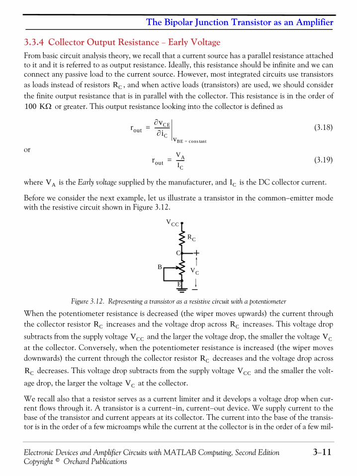
Electronic Devices and Amplifier Circuits with MATLAB Computing, Second Edition 3−11Copyright © Orchard Publications
The Bipolar Junction Transistor as an Amplifier
3.3.4 Collector Output Resistance − Early VoltageFrom basic circuit analysis theory, we recall that a current source has a parallel resistance attachedto it and it is referred to as output resistance. Ideally, this resistance should be infinite and we canconnect any passive load to the current source. However, most integrated circuits use transistorsas loads instead of resistors , and when active loads (transistors) are used, we should considerthe finite output resistance that is in parallel with the collector. This resistance is in the order of
or greater. This output resistance looking into the collector is defined as
(3.18)
or(3.19)
where is the Early voltage supplied by the manufacturer, and is the DC collector current.
Before we consider the next example, let us illustrate a transistor in the common−emitter modewith the resistive circuit shown in Figure 3.12.
Figure 3.12. Representing a transistor as a resistive circuit with a potentiometer
When the potentiometer resistance is decreased (the wiper moves upwards) the current throughthe collector resistor increases and the voltage drop across increases. This voltage drop
subtracts from the supply voltage and the larger the voltage drop, the smaller the voltage at the collector. Conversely, when the potentiometer resistance is increased (the wiper movesdownwards) the current through the collector resistor decreases and the voltage drop across
decreases. This voltage drop subtracts from the supply voltage and the smaller the volt-
age drop, the larger the voltage at the collector.
We recall also that a resistor serves as a current limiter and it develops a voltage drop when cur-rent flows through it. A transistor is a current−in, current−out device. We supply current to thebase of the transistor and current appears at its collector. The current into the base of the transis-tor is in the order of a few microamps while the current at the collector is in the order of a few mil-
RC
100 KΩ
rout∂vCE
∂iC-----------
vBE cons ttan=
=
routVAIC------=
VA IC
VCC
VC
E
B
C
RC
RC RC
VCC VC
RC
RC VCC
VC
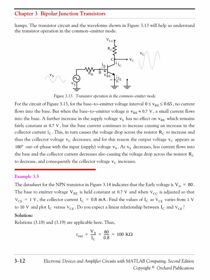
Chapter 3 Bipolar Junction Transistors
3−12 Electronic Devices and Amplifier Circuits with MATLAB Computing, Second EditionCopyright © Orchard Publications
liamps. The transistor circuit and the waveforms shown in Figure 3.13 will help us understandthe transistor operation in the common−emitter mode.
Figure 3.13. Transistor operation in the common−emitter mode
For the circuit of Figure 3.13, for the base−to−emitter voltage interval , no current
flows into the base. But when the base−to−emitter voltage is , a small current flows
into the base. A further increase in the supply voltage has no effect on which remainsfairly constant at , but the base current continues to increase causing an increase in thecollector current . This, in turn causes the voltage drop across the resistor to increase and
thus the collector voltage decreases. and for this reason the output voltage appears as
out−of−phase with the input (supply) voltage . As decreases, less current flows into
the base and the collector current decreases also causing the voltage drop across the resistor
to decrease, and consequently the collector voltage increases.
Example 3.5
The datasheet for the NPN transistor in Figure 3.14 indicates that the Early voltage is .
The base to emitter voltage is held constant at and when is adjusted so that
, the collector current . Find the values of as varies from
to and plot versus . Do you expect a linear relationship between and ?
Solution:Relations (3.18) and (3.19) are applicable here. Thus,
E
C
B
iB
iE
iC
VCC
vC
RB
RC
vBE
vS
vC
vS
0 vBE 0.65≤ ≤
vBE 0.7 V≈
vS vBE
0.7 ViC RC
vC vC
180° vS vS
RC
vC
VA 80=
VBE 0.7 V VCC
VCE 1 V= IC 0.8 mA= IC VCE 1 V
10 V IC VCE IC VCE
routVA
IC------- 80
0.8------- 100 KΩ= = =

Electronic Devices and Amplifier Circuits with MATLAB Computing, Second Edition 3−13Copyright © Orchard Publications
The Bipolar Junction Transistor as an Amplifier
Figure 3.14. Circuit for Example 3.5and
This expression shows that there is a linear relationship between and . The MATLAB
script below performs all computations and plots versus . The plot is shown in Figure 3.15.
vCE=1: 10; vA=80; iC1=0.8*10^(−3); r0=vA/iC1; iC=zeros(10,3);...iC(:,1)=vCE'; iC(:,2)=(vCE./r0)'; iC(:,3)=(iC1+vCE./r0)'; fprintf(' \n');...disp('vCE delta iC new iC');...disp('-------------------------');...fprintf('%2.0f \t %2.2e \t %2.2e\n',iC');...plot(vCE,iC(:,3)); xlabel('vCE (V)'); ylabel('iC (A)'); grid;...title('iC vs vCE for Example 3.5')
vCE delta iC new iC------------------------- 1 1.00e-005 8.10e-004 2 2.00e-005 8.20e-004 3 3.00e-005 8.30e-004 4 4.00e-005 8.40e-004 5 5.00e-005 8.50e-004 6 6.00e-005 8.60e-004 7 7.00e-005 8.70e-004 8 8.00e-005 8.80e-004 9 9.00e-005 8.90e-00410 1.00e-004 9.00e-004
Generally, the versus relation is non−linear. It is almost linear when a transistor operatesin the active region, and non−linear when it operates in the cutoff and saturation regions. Table3.2 shows the three modes of operation in a bipolar transistor and the forward or reverse−biasingof the emitter−base and collector−base junctions.
E
C
B
IB IC
RB VBEVS
VCC
VCE
RC
ΔiCΔvCE
rout------------ 10 5– ΔvCE= =
IC VCE
IC VCE
iC vCE
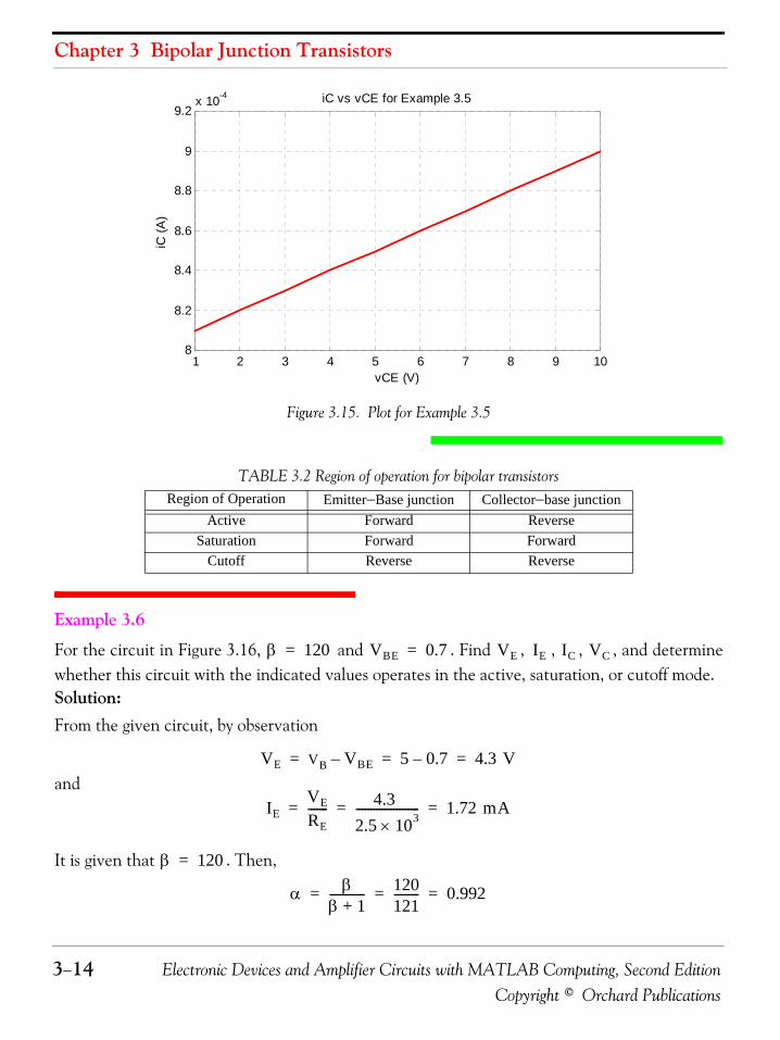
Chapter 3 Bipolar Junction Transistors
3−14 Electronic Devices and Amplifier Circuits with MATLAB Computing, Second EditionCopyright © Orchard Publications
Figure 3.15. Plot for Example 3.5
Example 3.6
For the circuit in Figure 3.16, and . Find , , , , and determinewhether this circuit with the indicated values operates in the active, saturation, or cutoff mode.Solution:From the given circuit, by observation
and
It is given that . Then,
TABLE 3.2 Region of operation for bipolar transistorsRegion of Operation Emitter−Base junction Collector−base junction
Active Forward ReverseSaturation Forward Forward
Cutoff Reverse Reverse
1 2 3 4 5 6 7 8 9 108
8.2
8.4
8.6
8.8
9
9.2x 10
-4
vCE (V)
iC (
A)
iC vs vCE for Example 3.5
β 120= VBE 0.7= VE IE IC VC
VE VB VBE– 5 0.7– 4.3 V= = =
IEVE
RE------- 4.3
2.5 103×---------------------- 1.72 mA= = =
β 120=
α ββ 1+------------ 120
121--------- 0.992= = =
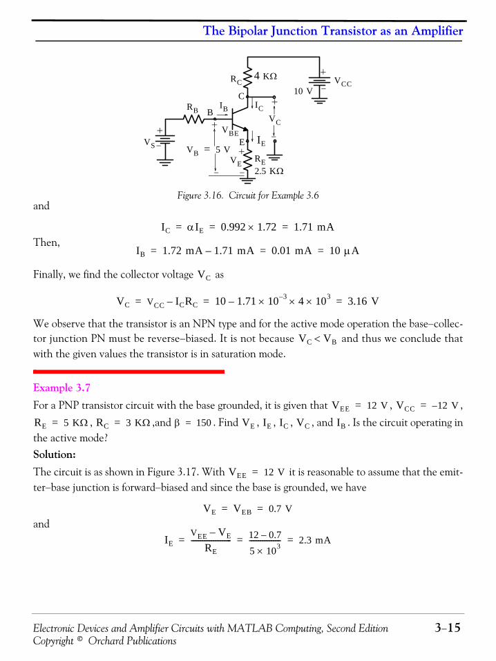
Electronic Devices and Amplifier Circuits with MATLAB Computing, Second Edition 3−15Copyright © Orchard Publications
The Bipolar Junction Transistor as an Amplifier
Figure 3.16. Circuit for Example 3.6and
Then,
Finally, we find the collector voltage as
We observe that the transistor is an NPN type and for the active mode operation the base−collec-tor junction PN must be reverse−biased. It is not because and thus we conclude thatwith the given values the transistor is in saturation mode.
Example 3.7 For a PNP transistor circuit with the base grounded, it is given that , ,
, ,and . Find , , , , and . Is the circuit operating inthe active mode?Solution:The circuit is as shown in Figure 3.17. With it is reasonable to assume that the emit-ter−base junction is forward−biased and since the base is grounded, we have
and
E
C
BIB ICRB
VBEVS
VCC
VC
VB 5 V=RE2.5 KΩ
IE
VE
4 KΩRC10 V
IC αIE 0.992 1.72× 1.71 mA= = =
IB 1.72 mA 1.71 mA– 0.01 mA 10 μA= = =
VC
VC VCC ICRC– 10 1.71 10 3–× 4 103××– 3.16 V= = =
VC VB<
VEE 12 V= VCC 12– V=
RE 5 KΩ= RC 3 KΩ= β 150= VE IE IC VC IB
VEE 12 V=
VE VEB 0.7 V= =
IEVEE VE–
RE---------------------- 12 0.7–
5 103×----------------- 2.3 mA= = =

Chapter 3 Bipolar Junction Transistors
3−16 Electronic Devices and Amplifier Circuits with MATLAB Computing, Second EditionCopyright © Orchard Publications
Figure 3.17. PNP transistor for Example 3.7With
Then,
and
With this value of , the collector−base junction is reverse−biased and the PNP transistor is inthe active mode. The base current is
Example 3.8
For the circuit in Figure 3.18, it is known that . Find , , , , , and . Isthe transistor operating in the active mode?Solution:
To simplify the part of the circuit to the left of the base, we apply Thevenin’s theorem at points and as shown in Figure 3.19, and denoting the Thevenin equivalent voltage and resistance as
and respectively, we find that
C
E
BIB
IEVEB VEE
VE
RC3 KΩ
ICVC
5 KΩRE
12 V
12 VVCC
β 150=α β
β 1+------------ 150
151--------- 0.993= = =
IC αIE 0.993 2.3 10 3–×× 2.28 mA= = =
VC RCIC VCC– 3 103× 2.28 10 3–×× 12– 5.16 V–= = =
VC
IB IE IC– 2.3 10 3–× 2.28 10 3–×– 20 μA= = =
β 120= IB IE IC VB VC VE
xy
VTH RTH
VTH VxyR2
R1 R2+------------------VS
3060 30+------------------12 4 V= = = =

Electronic Devices and Amplifier Circuits with MATLAB Computing, Second Edition 3−17Copyright © Orchard Publications
The Bipolar Junction Transistor as an Amplifier
Figure 3.18. Circuit for Example 3.8
Figure 3.19. Application of Thevenin’s theorem to the circuit of Example 3.8
and
The circuit in Figure 3.18 is thus reduced to that in Figure 3.20.
Figure 3.20. The circuit in Figure 3.18 after application of Thevenin’s theorem
Application of KVL around the left part of the circuit of Figure 3.20 yields
E
CBIB
IC
R2
VBE
VS
VCC
VC
VB RE
5 KΩ
IE
VE
8 KΩRC
12 V
12 V
R1
60 KΩ30 KΩ
R2VS 12 V
R1
60 KΩ30 KΩ
x
yVTH 4 V
RTH
20 KΩx
y
RTHR1 R2×R1 R2+------------------ 60 30×
60 30+------------------ 20 KΩ= = =
E
C
BIB IC
VBEVTH
VCC
VC
VB RE
5 KΩ
IE
VE
8 KΩRC
12 V
4 V
RTH
20 KΩ
RTHIB VBE REIE+ + VTH=
20 103×( )IB 0.7 5 103×( )IE+ + 4=
Chapter 3 Bipolar Junction Transistors
3−18 Electronic Devices and Amplifier Circuits with MATLAB Computing, Second EditionCopyright © Orchard Publications
From Table 3.1, . Then,
and
Next,
and
Also,
and
Since this is an NPN transistor and , the base−collector PN junction is reverse−biasedand thus the transistor is in active mode.
3.4 Transistor Amplifier Circuit Biasing
In our previous discussion, for convenience, a separate voltage source has been used to pro-
vide the necessary forward−bias voltage and another voltage source to establish a suitable
collector voltage where . However, it is not practical to use a separate
emitter−base bias voltage . This is because conventional batteries are not available for
. For this reason we use resistors in the order of kilohms to form voltage dividers withdesired values. In addition to eliminating the battery, some of these biasing methods compensatefor slight variations in transistor characteristics and changes in transistor conduction resultingfrom temperature irregularities.
4IB IE+ 3.35 103×----------------- 0.66 10 3–×= =
IE β 1+( )IB=
4IB β 1+( )IB+ 0.66 10 3–×=
125IB 0.66 10 3–×=
IB 5.28 10 6–× A 5.28 μA= =
IE β 1+( )IB 121 5.28 10 6–×× 0.639 mA= = =
VE REIE 5 103× 0.639 10 3–×× 3.2 V= = =
VB VBE VE+ 0.7 3.2+ 3.9 V= = =
IC IE IB– 0.639 10 3–× 5.28 10 6–×– 0.634 mA= = =
VC VCC= RCIC– 12 8 103× 0.634 10 3–××– 6.93 V= =
VC VB>
VBE
VCC
VC VC VCC RCIC–=
VBE
0.7 V
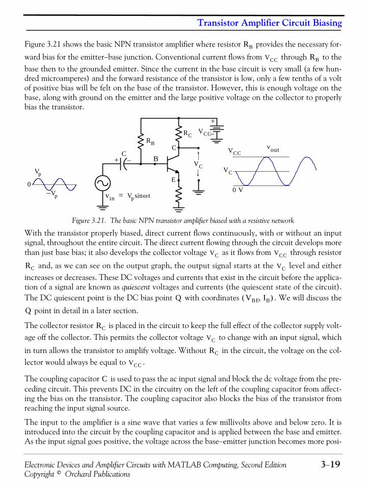
Electronic Devices and Amplifier Circuits with MATLAB Computing, Second Edition 3−19Copyright © Orchard Publications
Transistor Amplifier Circuit Biasing
Figure 3.21 shows the basic NPN transistor amplifier where resistor provides the necessary for-
ward bias for the emitter−base junction. Conventional current flows from through to thebase then to the grounded emitter. Since the current in the base circuit is very small (a few hun-dred microamperes) and the forward resistance of the transistor is low, only a few tenths of a voltof positive bias will be felt on the base of the transistor. However, this is enough voltage on thebase, along with ground on the emitter and the large positive voltage on the collector to properlybias the transistor.
Figure 3.21. The basic NPN transistor amplifier biased with a resistive network
With the transistor properly biased, direct current flows continuously, with or without an inputsignal, throughout the entire circuit. The direct current flowing through the circuit develops morethan just base bias; it also develops the collector voltage as it flows from through resistor
and, as we can see on the output graph, the output signal starts at the level and eitherincreases or decreases. These DC voltages and currents that exist in the circuit before the applica-tion of a signal are known as quiescent voltages and currents (the quiescent state of the circuit).The DC quiescent point is the DC bias point with coordinates . We will discuss the
point in detail in a later section.
The collector resistor is placed in the circuit to keep the full effect of the collector supply volt-age off the collector. This permits the collector voltage to change with an input signal, which
in turn allows the transistor to amplify voltage. Without in the circuit, the voltage on the col-lector would always be equal to .
The coupling capacitor is used to pass the ac input signal and block the dc voltage from the pre-ceding circuit. This prevents DC in the circuitry on the left of the coupling capacitor from affect-ing the bias on the transistor. The coupling capacitor also blocks the bias of the transistor fromreaching the input signal source.
The input to the amplifier is a sine wave that varies a few millivolts above and below zero. It isintroduced into the circuit by the coupling capacitor and is applied between the base and emitter.As the input signal goes positive, the voltage across the base−emitter junction becomes more posi-
RB
VCC RB
E
C
B
VCC
+ −C
RB
RC
vin Vp ωtsin=
VC
+
−
V– p
Vp
0
VC
VCC
0 V
vout
VC VCC
RC VC
Q VBE IB,( )
Q
RC
VC
RC
VCC
C

Chapter 3 Bipolar Junction Transistors
3−20 Electronic Devices and Amplifier Circuits with MATLAB Computing, Second EditionCopyright © Orchard Publications
tive. This in effect increases forward bias, which causes base current to increase at the same rateas that of the input sine wave. Collector and emitter currents also increase but much more thanthe base current. With an increase in collector current, more voltage is developed across .
Since the voltage across and the voltage across the transistor (collector to emitter) must add
up to , an increase in voltage across results in an equal decrease in voltage across thetransistor. Therefore, the output voltage from the amplifier, taken at the collector of the transis-tor with respect to the emitter, is a negative alternation of voltage that is larger than the input,but has the same sine wave characteristics.
During the negative alternation of the input, the input signal opposes the forward bias. Thisaction decreases base current, which results in a decrease in both collector and emitter currents.The decrease in current through decreases its voltage drop and causes the voltage across thetransistor to rise along with the output voltage. Therefore, the output for the negative alterna-tion of the input is a positive alternation of voltage that is larger than the input but has the samesine wave characteristics.
By examining both input and output signals for one complete alternation of the input, we can seethat the output of the amplifier is an exact reproduction of the input except for the reversal inpolarity and the increased amplitude (a few millivolts as compared to a few volts).
Figure 3.22 shows the basic PNP transistor amplifier. As we already know, the primary differencebetween the NPN and PNP amplifier is the polarity of the source voltage . With a negative
, the PNP base voltage is slightly negative with respect to ground, which provides the neces-sary forward bias condition between the emitter and base.
Figure 3.22. The basic PNP transistor amplifier
When the PNP input signal goes positive, it opposes the forward bias of the transistor. Thisaction cancels some of the negative voltage across the emitter−base junction, which reduces thecurrent through the transistor. Therefore, the voltage across decreases, and the voltage
RC
RC
VCC RC
RC
VCC
VCC
E
C
B
VCC
+ −C
RB
RC
vin Vp ωtsin=
+−
VC
V– p
Vp
0
VC
VCC
0 V
vout
RC
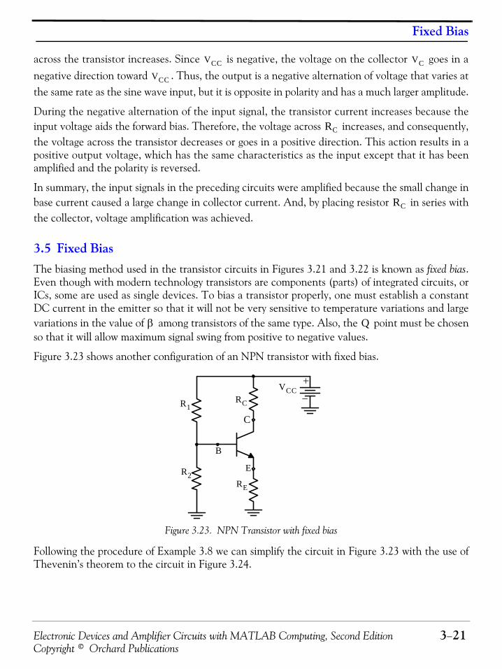
Electronic Devices and Amplifier Circuits with MATLAB Computing, Second Edition 3−21Copyright © Orchard Publications
Fixed Bias
across the transistor increases. Since is negative, the voltage on the collector goes in anegative direction toward . Thus, the output is a negative alternation of voltage that varies atthe same rate as the sine wave input, but it is opposite in polarity and has a much larger amplitude.
During the negative alternation of the input signal, the transistor current increases because theinput voltage aids the forward bias. Therefore, the voltage across increases, and consequently,the voltage across the transistor decreases or goes in a positive direction. This action results in apositive output voltage, which has the same characteristics as the input except that it has beenamplified and the polarity is reversed.
In summary, the input signals in the preceding circuits were amplified because the small change inbase current caused a large change in collector current. And, by placing resistor in series withthe collector, voltage amplification was achieved.
3.5 Fixed BiasThe biasing method used in the transistor circuits in Figures 3.21 and 3.22 is known as fixed bias.Even though with modern technology transistors are components (parts) of integrated circuits, orICs, some are used as single devices. To bias a transistor properly, one must establish a constantDC current in the emitter so that it will not be very sensitive to temperature variations and largevariations in the value of among transistors of the same type. Also, the point must be chosenso that it will allow maximum signal swing from positive to negative values.
Figure 3.23 shows another configuration of an NPN transistor with fixed bias.
Figure 3.23. NPN Transistor with fixed bias
Following the procedure of Example 3.8 we can simplify the circuit in Figure 3.23 with the use ofThevenin’s theorem to the circuit in Figure 3.24.
VCC VC
VCC
RC
RC
β Q
E
C
B
VCC
R1RC
RE
R2
+
−
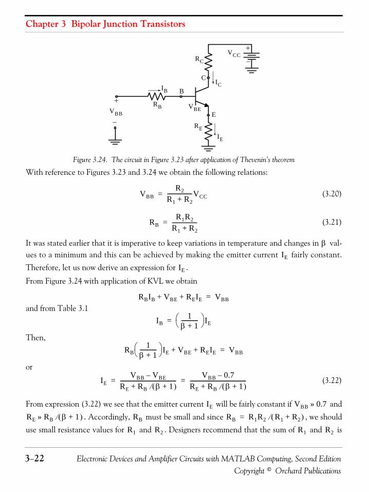
Chapter 3 Bipolar Junction Transistors
3−22 Electronic Devices and Amplifier Circuits with MATLAB Computing, Second EditionCopyright © Orchard Publications
Figure 3.24. The circuit in Figure 3.23 after application of Thevenin’s theorem
With reference to Figures 3.23 and 3.24 we obtain the following relations:
(3.20)
(3.21)
It was stated earlier that it is imperative to keep variations in temperature and changes in val-ues to a minimum and this can be achieved by making the emitter current fairly constant.
Therefore, let us now derive an expression for .
From Figure 3.24 with application of KVL we obtain
and from Table 3.1
Then,
or
(3.22)
From expression (3.22) we see that the emitter current will be fairly constant if and
. Accordingly, must be small and since , we should
use small resistance values for and . Designers recommend that the sum of and is
E
C
B
VCCRC
RE
RBVBB
IB
VBE
IE
+
−
+
−
IC
VBBR2
R1 R2+------------------VCC=
RBR1R2
R1 R2+------------------=
βIE
IE
RBIB VBE REIE+ + VBB=
IB1
β 1+------------⎝ ⎠
⎛ ⎞ IE=
RB1
β 1+------------⎝ ⎠
⎛ ⎞ IE VBE REIE+ + VBB=
IEVBB VBE–
RE RB β 1+( )⁄+----------------------------------------- VBB 0.7–
RE RB β 1+( )⁄+-----------------------------------------= =
IE VBB 0.7»
RE RB β 1+( )⁄» RB RB R1R2 R1 R2+( )⁄=
R1 R2 R1 R2

Electronic Devices and Amplifier Circuits with MATLAB Computing, Second Edition 3−23Copyright © Orchard Publications
Fixed Bias
such that the current through them (assuming that the base current is zero) is about half of theemitter current . It is also recommended that , or , and the product each
be close to one−third of the value of .
It is often said that the emitter resistor provides a negative feedback action which stabilizes
the bias current. To understand how this is done, let us assume that the emitter current
increases. In this case, the voltages and will also increase. But the base voltage being
determined by the voltage division provided by resistors and will remain relatively con-
stant and according to KVL, the base−to−emitter voltage will decrease. And since
, both the collector current and emitter current will decrease. Obviously,
this is a contradiction to our original assumption (increase in ) and thus we say that the emitter
resistor provides a negative feedback action.
Let us consider the transistor circuit in Figure 3.23 which is repeated as Figure 3.25 for conve-nience.
Figure 3.25. NPN transistor with fixed bias
Circuit designers maintain that if we specify the voltage, the current, and the value of ,we can determine the appropriate values of the four resistors for proper biasing by letting the val-ues of , or , and the product each be close to one−third of the value of ,
and assuming that the base current is negligible, the current through resistors and is
. For convenience, we will denote the sum of and as .
Example 3.9
For the transistor circuit of Figure 3.26 . Find the values of the four resistors for appro-priate fixed biasing.
IE VBB VCB VCB RCIC
VCC
RE
IE
REIE VE
R1 R2
VBE
IC IreVBE VT⁄
= IC IE
IE
RE
E
C
B
VCC
R1
RC
RE
R2
IE
IR
IB 0≈E
C
B
VCCRC
RE
RB
VBBIB VBE
IE
+
−+
−
+
−
VCC IE β
VBB VCB VCB RCIC VCC
IR R1 R2
IR 0.5IE= R1 R2 Req
β 120=

Chapter 3 Bipolar Junction Transistors
3−24 Electronic Devices and Amplifier Circuits with MATLAB Computing, Second EditionCopyright © Orchard Publications
Figure 3.26. Transistor circuit for Example 3.9Solution:The given circuit and its Thevenin equivalent are shown in Figure 3.27. The Thevenin equiva-lent is shown just to indicate the value of which will be used in the calculations.
Figure 3.27. The transistor circuit in Example 3.9 and its Thevenin equivalent
As stated above, it is suggested that the values of , or , and the product each
be close to one−third of the value of , and assuming that the base current is negligible, the
current through resistors and is . Then,
and with reference to the Thevenin equivalent circuit above, since by KVL
E
C
B
VCC
R1RC
RE
R2
+
−15 V
IE
VBB
E
C
B
VCC
R1
RC
RE
R2
IE
IR
IB 0≈E
C
B
VCCRC
RE
RB
VBBIB VBE
IE
+
−+
−
+
−
15 V VCC
IC
VBB VCB VCB RCIC
VCC
IR R1 R2 IR 0.5IE=
VBB13---VCC
13---15 5 V= = =
IB 0≈
VBE REIE+ VBB=
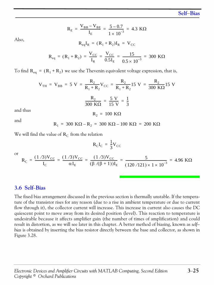
Electronic Devices and Amplifier Circuits with MATLAB Computing, Second Edition 3−25Copyright © Orchard Publications
Self−Bias
Also,
To find we use the Thevenin equivalent voltage expression, that is,
and thus
and
We will find the value of from the relation
or
3.6 Self−BiasThe fixed bias arrangement discussed in the previous section is thermally unstable. If the tempera-ture of the transistor rises for any reason (due to a rise in ambient temperature or due to currentflow through it), the collector current will increase. This increase in current also causes the DCquiescent point to move away from its desired position (level). This reaction to temperature isundesirable because it affects amplifier gain (the number of times of amplification) and couldresult in distortion, as we will see later in this chapter. A better method of biasing, known as self−bias is obtained by inserting the bias resistor directly between the base and collector, as shown inFigure 3.28.
REVBB VBE–
IE-------------------------- 5 0.7–
1 10 3–×------------------- 4.3 KΩ= = =
ReqIR R1 R2+( )IR VCC= =
Req R1 R2+( )VCC
IR---------- VCC
0.5IE------------ 15
0.5 10 3–×------------------------ 300 KΩ= = = = =
Req R1 R2+( )=
VTH VBB 5 VR2
R1 R2+------------------VCC
R2
R1 R2+------------------15 V
R2
300 KΩ--------------------15 V= = = = =
R2
300 KΩ-------------------- 5 V
15 V------------ 1
3---= =
R2 100 KΩ=
R1 300 KΩ R2– 300 KΩ 100 KΩ– 200 KΩ= = =
RC
RCIC13---VCC=
RC1 3⁄( )VCC
IC------------------------- 1 3⁄( )VCC
αIE------------------------- 1 3⁄( )VCC
β β 1+( )⁄( )IE---------------------------------- 5
120 121⁄( ) 1 10 3–××---------------------------------------------------- 4.96 KΩ= = = = =

Chapter 3 Bipolar Junction Transistors
3−26 Electronic Devices and Amplifier Circuits with MATLAB Computing, Second EditionCopyright © Orchard Publications
Figure 3.28. NPN transistor amplifier with self−bias
By tying the collector to the base in this manner, feedback voltage can be fed from the collectorto the base to develop forward bias. Now, if an increase of temperature causes an increase in col-lector current, the collector voltage will fall because of the increase of voltage produced
across the collector resistor . This drop in will be fed back to the base and will result in adecrease in the base current. The decrease in base current will oppose the original increase incollector current and tend to stabilize it. The exact opposite effect is produced when the collectorcurrent decreases.
From Figure 3.28,
(3.23)
From (3.23) we see that to maintain the emitter current fairly constant, we should choose the
collector and base resistors such that .
Example 3.10
For the transistor circuit in Figure 3.29 and we want the collector voltage to vary inaccordance with and . Find the values of and tomeet these specifications.
E
C
B
VCC
RB
RC
IB
IC
IE
IB IC+ IE=
VC
RL VC
RCIE RBIB VBE+ + VCC=
RCIE RB1
β 1+------------IE VBE+ + VCC=
IEVCC VBE–
RC RB β 1+( )⁄+-----------------------------------------=
IE
RB β 1+( )⁄ RC«
β 120=
VC 3 ωt Vsin VBE+= IE 1 mA= RC RB

Electronic Devices and Amplifier Circuits with MATLAB Computing, Second Edition 3−27Copyright © Orchard Publications
Self−Bias
Figure 3.29. Transistor circuit for Example 3.10Solution:
We assign current directions as shown in Figure 3.30.
Figure 3.30. Circuit for Example 3.10 with assigned current directions
By inspection,
or
Also, by inspection
E
C
B
VCC
RB
RC15 V
E
C
B
VCC
RB
RC
IB
IC
IE
IB IC+ IE=
15 V
VC RBIB VBE+ RB1
β 1+------------⎝ ⎠
⎛ ⎞ IE 0.7+ 3 ωtsin 0.7+ 3 0.7+= = = =
RB3
1 10 3–× 1 121⁄( )×---------------------------------------------- 363 KΩ= =
VC VCC RCIE–=
RCVCC VC–
IE----------------------- 15 3.7–
1 10 3–×------------------- 11.3 KΩ= = =

Chapter 3 Bipolar Junction Transistors
3−28 Electronic Devices and Amplifier Circuits with MATLAB Computing, Second EditionCopyright © Orchard Publications
3.7 Amplifier Classes and OperationIn the previous discussions we assumed that for every portion of the input signal there was anoutput from the amplifier. This is not always the case with all types of amplifiers. It may be desir-able to have the transistor conducting for only a portion of the input signal. The portion of theinput for which there is an output determines the class of operation of the amplifier. There arefour classes of amplifier operations. They are Class A, Class B, Class AB, and Class C.
Before discussing the different classes of amplifiers, we should remember that every amplifier hassome unavoidable limitations on its performance. The most important that we need to be con-cerned about when choosing and using them are:
• Limited bandwidth. For each amplifier there is an upper frequency beyond which it finds itimpossible to amplify signals.
• Noise. All electronic devices tend to add some random noise to the signals passing throughthem, hence degrading the SNR (signal to noise ratio). This, in turn, limits the accuracy of anymeasurement or communication.
• Limited output voltage, current, and power levels. A given amplifier cannot output signalsabove a particular level; there is always a finite limit to the output signal size.
• Distortion. The actual signal pattern will be altered due non−linearities in the amplifier. Thisalso reduces the accuracy of measurements and communications.
• Finite gain. A given amplifier may have a high gain, but this gain cannot normally be infiniteso may not be large enough for a given purpose. This is why we often use multiple amplifiers orstages to achieve a desired overall gain.
Let us first discuss the limits to signal size. Figure 3.31(a) shows a simple amplifier being used todrive output signals into a resistive load. The power supply voltages are and andthus the output voltage will be limited to the range
From our earlier discussion we can think of the transistor as a variable resistor between the col-lector resistor and emitter resistor . We denote this variable resistor, i.e., the transistor, as
and its value depends on the input voltage . The two extreme values of the variable resis-
tor are (open circuit) and (short circuit). These conditions are shown in Fig-ures 3.31(b) and 3.31(c).
+VCC VEE–
vout
VEE– vout +VCC< <
RC RE
Rtr vin
Rtr ∞= Rtr 0=

Electronic Devices and Amplifier Circuits with MATLAB Computing, Second Edition 3−29Copyright © Orchard Publications
Amplifier Classes and Operation
Figure 3.31. Simple amplifier with resistive load
Application of the voltage division expression for the circuit in Figure 3.31(b) yields the maximumvoltage across the load resistor, that is,
(3.24)
and the corresponding maximum current is
(3.25)
Obviously, we want the power delivered to the load resistor to be maximum; therefore, we mustmake the collector resistor much smaller than the load resistor , that is, to
maximize the current through the load resistor. For convenience, we choose to be one−tenthof the value of , that is,
(3.26)
Next, by application of Thevenin’s theorem for the circuit of Figure 3.31(c) where the load resis-tor is disconnected, we redraw the circuit as shown in Figure 3.32.
Figure 3.32. Thevenin equivalent for the circuit in Figure 3.31(c).
From Figure 3.32,
E
C
VCC
RE
RC
VEE
RloadvoutRtr ∞= Rtr 0=
a( ) b( ) c( )
RC RC
VCC VCC
B B BC C
E ERE RE
VEE VEE
Rloadvout voutRload
vout max( )Rload
RC Rload+------------------------- VCC⋅=
iout max( )VCC
RC Rload+-------------------------=
RC Rload RC Rload«
RC
Rload
RC 0.1Rload=
VCC
RERC
VEE
Rload vout
I
VTH
RTH
VTH

Chapter 3 Bipolar Junction Transistors
3−30 Electronic Devices and Amplifier Circuits with MATLAB Computing, Second EditionCopyright © Orchard Publications
(3.27)
(3.28)
and thus(3.29)
From (3.29) we see that for to be close to , the Thevenin resistance shown
in (3.28) and (3.29) should be minimized. We already have minimized to be ,
so let us make one−tenth of , that is, , or
(3.30)
Example 3.11 Let us suppose that the circuit of Figure 3.33 is to be used as the output stage of an audio systemwhose load resistance is and the supply voltages are and
. Taken into account the recommendations discussed above for sizing the emitterand collector resistors, find the power absorbed by the combination of the collector resistor, thetransistor, and the emitter resistor when and the amplifier is on.
Figure 3.33. Circuit for Example 3.11
IVCC VEE+
RC RE+------------------------=
VTH VCC RCI–REVCC RCVEE–
RC RE+--------------------------------------= =
RTHRCRE
RC RE+-------------------=
vout min( )Rload
RTH Rload+----------------------------VTH=
vout min( ) VEE– RTH
RC RC 0.1Rload=
RE RC RE 0.1RC=
RE 0.01Rload=
Rload 8 Ω= VCC +24V=
VEE 24V–=
vout 0 V=
E
C
B
VCC
RE
RC
vin
VEE
Rload vout

Electronic Devices and Amplifier Circuits with MATLAB Computing, Second Edition 3−31Copyright © Orchard Publications
Amplifier Classes and Operation
Solution:
With and , there is no current through the load
resistor and since , , that is, the amplifier will be draw-
ing from the positive power supply. Since there is no current through the load, this currentwill flow through the transistor and the emitter resistor and into the negative power supply. Thus,the power absorbed by the combination of the collector resistor , the transistor, and the emit-
ter resistor will be . This is indeed a very large amountof power and thus this amplifier is obviously very inefficient.
For a comparison of output signals for the different amplifier classes of operation, please refer toFigure 3.34 during the following discussion.
Figure 3.34. Output signals for Class A, Class B, Class AB, and Class C amplifiers
We should remember that the circuits presented in our subsequent discussion are only the outputstages of an amplifier to provide the necessary drive to the load.
3.7.1 Class A Amplifier OperationClass A amplifiers are biased so that variations in input signal polarities occur within the limits ofcutoff and saturation. In a PNP transistor, for example, if the base becomes positive with respectto the emitter, holes will be repelled at the PN junction and no current can flow in the collectorcircuit. This condition is known as cutoff. Saturation occurs when the base becomes so negativewith respect to the emitter that changes in the signal are not reflected in collector−current flow.
Biasing an amplifier in this manner places the DC operating point between cutoff and saturationand allows collector current to flow during the complete cycle (360 degrees) of the input signal,thus providing an output which is a replica of the input. Figure 3.35 is an example of a Class Aamplifier. Although the output from this amplifier is 180 degrees out−of−phase with the input, theoutput current still flows for the complete duration of the input.
Class A amplifiers are used as amplifiers in radio, radar, and sound systems.
The output stages of Class A amplifiers carry a fairly large current. This current is referred to a qui-escent current and it is defined as the current in the amplifier when the output voltage is zero.
RC 0.1Rload 0.1 8× 0.8 Ω= = = vout 0 V=
RCIC vout+ 24 V= IC 24 0.8⁄ 30 A= =
30 A
RC
RE 30 24 24+( )× 1440 w 1.44 Kw= =
Class A Class B Class AB Class C

Chapter 3 Bipolar Junction Transistors
3−32 Electronic Devices and Amplifier Circuits with MATLAB Computing, Second EditionCopyright © Orchard Publications
In Example 3.11 we learned that the arrangement of the circuit in Figure 3.33 is very inefficient.However, a Class A amplifier can be made more efficient if we employ a push−pull* arrangementas shown in Figure 3.36.
Figure 3.35. Typical Class A amplifier
Figure 3.36. Push−Pull Output stage for a Class A amplifier
From the circuit in Figure 3.36, it is evident that we can control the currents and by varying
the input voltages and . It is convenient to set the quiescent current, denoted as , to
one−half the maximum current drawn by the load. Then, we can adjust the currents and tobe equal and opposite. Then,
* The expression push−pull (or double ended) derives its name from the fact that one of the two transistors pushes (sources)current into the load during the positive cycle while the other pulls (sinks) current from the load during the negative cycle.
E
C
B
VCC
+ −C
RB
RC
vin Vp ωtsin=
+−
VC
V– p
Vp
0
VC
VCC
0 V
vout
i2
i1
iload
RE1
RE2
vin1
vin2 Rload
VEE
+
−
vout
+
+
−
−
VEE
i1 i2
vin1 vin2 IQ
i1 i2

Electronic Devices and Amplifier Circuits with MATLAB Computing, Second Edition 3−33Copyright © Orchard Publications
Amplifier Classes and Operation
(3.31)
and(3.32)
The currents and in each transistor vary from to ; therefore, the load current is within
the range .
Example 3.12
In the circuit in Figure 3.37, , , and . Compute the
power absorbed by the circuit if we want to apply up to to the load.
Figure 3.37. Circuit for Example 3.12
Solution:The maximum load current is
and the quiescent current is
Then, each transistor will absorb
and the total power absorbed by the circuit is
i1 IQiload
2----------+=
i2 IQiload
2----------–=
i1 i2 0 2IQ
2IQ– iload 2IQ≤ ≤
+VEE 24 V= V– EE 24 V–= Rload 8 Ω=
24 V 8 Ω
i2
i1
iload
RE1
RE2
vin1
vin2Rload
VEE
+
−
vout
+
+
−
−
VEE
24 V
8 Ω
24 V
iload max( ) 24 V8 Ω------------ 3 A= =
IQ3 A
2--------- 1.5 A= =
P 24 1.5× 36 w= =
Chapter 3 Bipolar Junction Transistors
3−34 Electronic Devices and Amplifier Circuits with MATLAB Computing, Second EditionCopyright © Orchard Publications
This is not very efficient, but it is much more efficient than the circuit in the previous example.
3.7.2 Class B Amplifier OperationThe circuit in Figure 3.38 shows the output stage of a Class B amplifier. This consists also of apush−pull arrangement but the bases (inputs) are tied by two diodes. The current in the diodes issupplied by two current sources denoted as .
Figure 3.38. Output stage in a typical Class B amplifier
When goes positive, the upper transistor conducts and the lower transistor is cutoff. Then,
the input to the base of the upper transistor is and the voltage at the emitter terminal
of the upper transistor is , and since , we find that
for (3.33)
When goes negative, the upper transistor is cutoff and the lower transistor conducts. then
the input to the base of the lower transistor is and the voltage at the emitter terminal of
the lower transistor is , and since , we find that
Ptotal 2 36× 72 w= =
Ibias
v1
i1
iload
RE2
RE1
vin
Rload
VCC
Ibias
Ibias
v2
vD1
vD2
vBE1 −
vEB2
+
+
+
−
−
−+
+vout−
VCCRC1
RC2
vin
vin vD1+
v1 vin vD1 vBE1–+= vBE1 vD1=
v1 vin= vin 0>
vin
vin vD2–
v2 vEB2 vin vD2–+= vEB2 vD2=

Electronic Devices and Amplifier Circuits with MATLAB Computing, Second Edition 3−35Copyright © Orchard Publications
Amplifier Classes and Operation
for (3.34)
From (3.33) and (3.34) we conclude that
(3.35)
Therefore, when , , and also, and the current and the output of both
transistors including the quiescent currents will be zero also, and the power absorbed by thecircuit will be zero. Accordingly, it appears that this arrangement has perfect efficiency. However,this ideal condition is never achieved because no two diodes or two transistors are exactly identi-cal. There exists a range where both transistors are cutoff when the input signal changes polarityand this results in crossover distortion as shown in Figure 3.39. This distortion is due to the non−lin-earities in transistor devices where the output does not vary linearly with the input.
Figure 3.39. Crossover distortion in Class B amplifier
The efficiency of a typical Class B amplifier varies between 65 to 75 percent.
3.7.3 Class AB Amplifier OperationWe’ve seen that Class A amplifiers are very inefficient, and Class B amplifiers although are effi-cient, they produce crossover distortion. Class AB amplifiers combine the advantages of Class Aand Class B amplifiers while they minimize the problems associated with them. Two possiblearrangements for the output stage of a typical Class AB amplifier are shown in Figure 3.40.
In Figure 3.40(a) the voltage at the upper transistor is , and since
, we find that and similarly for the lower transistor
. Then, when , we have
(3.36)
and the quiescent current, assuming that , is
(3.37)
v2 vin= vin 0<
v1 v2 vin= =
vin 0= v1 0= v2 0=
Ibias
Crossover distortion
voutvin
v1 v1 vin vD1 vD2 vBE1–+ +=
vBE1 vD1 vD2= = v1 vin vD+=
v2 vin vD–= vin 0=
v1 v2– 2vD=
RE1 RE2=
Ibiasv1 v2–
RE1 RE2+------------------------ 2vD
2RE---------- vD
RE------= ==

Chapter 3 Bipolar Junction Transistors
3−36 Electronic Devices and Amplifier Circuits with MATLAB Computing, Second EditionCopyright © Orchard Publications
Figure 3.40. Two possible arrangements for the output stage in a typical Class AB amplifier
For small output signals that require currents in the range both transistorswill conduct and will behave as Class A amplifier. But for larger signals, one transistor will con-duct and supply the current required by the load, while the other will be cutoff. In other words,for large signals the circuit of Figure 3.40(a) acts like a Class B amplifier and hence the nameClass AB amplifier.For sinusoidal signals into the load , the RMS voltage will be
(3.38)
and the output power will be
(3.39)
For maximum power, we should make as small as possible, so let , and let
and . Then,
v1
i1
iload
RE2
RE1
Rload
VCC
VCC
+
−vout
Ibias
v2
vD1
vD2
vBE1+
−
vEB2vD4
v1
i1
vin
Ibias
v2
+
−B
AR1
Radj
R2
vAB
−
−
+
+
Ibias
RC1
RC2
+−
vin
Ibias
+
+
+−
VCC
VCC
+−vBE1
vout−Rload+
−vEB2
RE1
RE2vD3
−
(a) (b)
iload
2Ibias– iload 2Ibias< <
Rload
vout RMS( )2vD
RE------------- Rload⋅=
Pload2vD
2
RE2
--------- Rload⋅=
RE RE 0.5 Ω=
Rload 8 Ω= vD 0.5 V=

Electronic Devices and Amplifier Circuits with MATLAB Computing, Second Edition 3−37Copyright © Orchard Publications
Amplifier Classes and Operation
If we let and , the total power absorbed will be
For the circuit in Figure 3.40(b), the voltage can be adjusted to any desired value by selecting
appropriate values for resistors and . The adjustable resistor is set to a position to yield
the desired value of the quiescent current .
From the above discussion, we have seen that the Class AB amplifier maintains current flow at alltimes so that the output devices can begin operation nearly instantly without the crossover distor-tion in Class B amplifiers. However, complete current is not allowed to flow at any one time thusavoiding much of the inefficiency of the Class A amplifier. Class AB designs are about 50 percentefficient (half of the power supply is power is turned into output to drive speakers) compared toClass A designs at 20 percent efficiency.Class AB amplifiers are the most commonly used amplifier designs due to their attractive combi-nation of good efficiency and high−quality output (low distortion and high linearity close to butnot equal to Class A amplifiers).
3.7.4 Class C Amplifier OperationClass C amplifiers have high efficiency and find wide applications in continuous wave (CW) laserand radar applications, in frequency modulation (FM), and phase and pulse amplification. How-ever, Class C amplifiers cannot be used with amplitude modulation (AM) because of the high dis-tortion. A typical Class C output stage is shown in Figure 3.41.
Figure 3.41. Output stage in a typical Class C amplifier
In Class C amplifier operation, the transistor in Figure 3.41 behaves as a open−closed switch. Theload can be thought of as an antenna. During the positive half−cycle the transistor behaves like aclosed switch, current flows through the inductor and creates a magnetic field, and at the same
time the capacitor discharges and thus the two currents flow through the emitter to the
Pload2vD
2
RE2
--------- Rload⋅ 0.50.25---------- 8× 20 w= = =
VCC 24 V= Ibias 1 A=
Ptotal 24 1 20+× 44 w= =
vAB
R1 R2 Radj
Ibias
VCCL
vBE+
−
−+
C
vin
iC
iL
iC iL+Load
+
−
iL
iC iL+
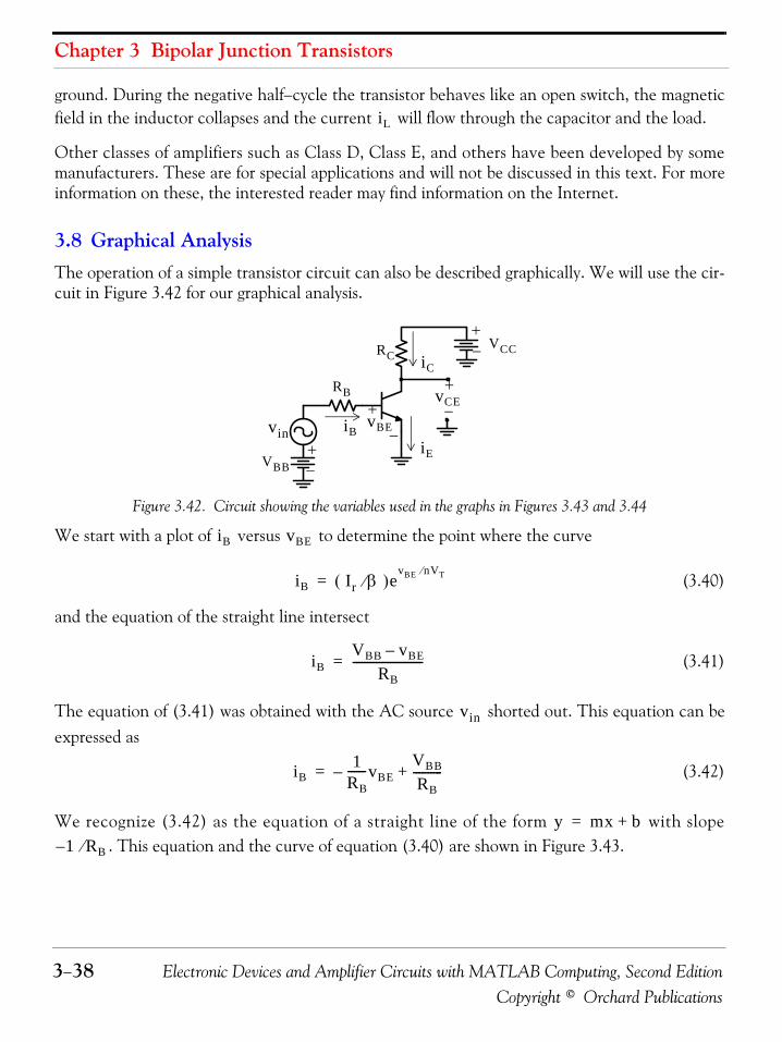
Chapter 3 Bipolar Junction Transistors
3−38 Electronic Devices and Amplifier Circuits with MATLAB Computing, Second EditionCopyright © Orchard Publications
ground. During the negative half−cycle the transistor behaves like an open switch, the magneticfield in the inductor collapses and the current will flow through the capacitor and the load.
Other classes of amplifiers such as Class D, Class E, and others have been developed by somemanufacturers. These are for special applications and will not be discussed in this text. For moreinformation on these, the interested reader may find information on the Internet.
3.8 Graphical AnalysisThe operation of a simple transistor circuit can also be described graphically. We will use the cir-cuit in Figure 3.42 for our graphical analysis.
Figure 3.42. Circuit showing the variables used in the graphs in Figures 3.43 and 3.44
We start with a plot of versus to determine the point where the curve
(3.40)
and the equation of the straight line intersect
(3.41)
The equation of (3.41) was obtained with the AC source shorted out. This equation can beexpressed as
(3.42)
We recognize (3.42) as the equation of a straight line of the form with slope. This equation and the curve of equation (3.40) are shown in Figure 3.43.
iL
VCCRC
vBE
+−
vin
iC
VBB
+
−
+
−vCE
iB
RB
+−
iE
iB vBE
iB Ir β⁄( )evBE nVT⁄
=
iBVBB vBE–
RB------------------------=
vin
iB1
RB------vBE–
VBB
RB----------+=
y mx b+=
1 RB⁄–
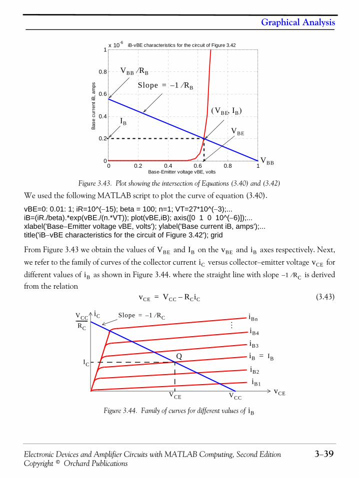
Electronic Devices and Amplifier Circuits with MATLAB Computing, Second Edition 3−39Copyright © Orchard Publications
Graphical Analysis
Figure 3.43. Plot showing the intersection of Equations (3.40) and (3.42)
We used the following MATLAB script to plot the curve of equation (3.40).
vBE=0: 0.01: 1; iR=10^(−15); beta = 100; n=1; VT=27*10^(−3);...iB=(iR./beta).*exp(vBE./(n.*VT)); plot(vBE,iB); axis([0 1 0 10^(−6)]);...xlabel('Base−Emitter voltage vBE, volts'); ylabel('Base current iB, amps');...title('iB−vBE characteristics for the circuit of Figure 3.42'); grid
From Figure 3.43 we obtain the values of and on the and axes respectively. Next,
we refer to the family of curves of the collector current versus collector−emitter voltage for
different values of as shown in Figure 3.44. where the straight line with slope is derivedfrom the relation
(3.43)
Figure 3.44. Family of curves for different values of
0 0.2 0.4 0.6 0.8 10
0.2
0.4
0.6
0.8
1x 10
-6
Base-Emitter voltage vBE, volts
Bas
e cu
rren
t iB
, am
ps
iB-vBE characteristics for the circuit of Figure 3.42
VBE IB,( )IB
Slope 1 RB⁄–=
VBE
VBB RB⁄
VBB
VBE IB vBE iB
iC vCE
iB 1 RC⁄–
vCE VCC RCiC–=
VCE VCC
QIC
iB IB=
Slope 1 RC⁄–=
vCE
iC
iB1
iB2
iB3
iB4
iBn…VCCRC
---------
iB

Chapter 3 Bipolar Junction Transistors
3−40 Electronic Devices and Amplifier Circuits with MATLAB Computing, Second EditionCopyright © Orchard Publications
Solving (3.43) for we obtain
* (3.44)
As shown in Figure 3.44, this straight line, commonly known as load line, and the curve
intersect at point whose coordinates are the DC bias values and . Obviously, the value
of the collector resistor must be chosen such that the load line is neither a nearly horizontalnor a nearly vertical line.
Example 3.13
For the circuit in Figure 3.45, the input voltage is a sinusoidal waveform. Using the versus
and versus curves shown in Figure 3.46, sketch the waveforms for , , , and
.
Figure 3.45. Circuit for Example 3.13
Solution:
Let . We draw three parallel lines with slope , one corresponding to input
, the second at , and the third at as shown in Figure 3.47. The
input voltage is superimposed on the DC bias voltage .
* We observe that (3.40) describes an equation of a straight line of the form where the slope is
and the ordinate axis intercept is .
iC
iC1
RC------– vCE
VCC
RC----------+=
y mx b+= m 1 RC⁄–=
b VCC RC⁄=
iB IB=
Q VCE IC
RC
vi iB
vBE iC vCE vBE iB vCE
iC
VCCRC
vBE
+−
vin
iC
VBB
+
−
+
−vCE
iB
RB
+−
iE
vin Vp ωtsin= 1 RB⁄–
vin 0= vin Vp= vin V– p=
vin VBB

Electronic Devices and Amplifier Circuits with MATLAB Computing, Second Edition 3−41Copyright © Orchard Publications
Graphical Analysis
Figure 3.46. versus and versus curves for Example 3.13
Figure 3.47. Graphical representation of and when the input voltage is a sinusoid
Figure 3.48 is the graphical representation of and when the input voltage is a sinusoid.
VCEVCC
QIC iB IB=
Slope 1 RC⁄–=
vCE
iC
…VCCRC
---------
iB
vBE
QIB
VBE
Slope 1 RB⁄–=
VBB
VBBRB
---------
iB vBE iC vCE
iB
vBE
QIB
VBE
Slope 1 RB⁄–=
VBB
VBBRB
---------
vin
vBE
iB
vBE iB vin
vCE iC vin

Chapter 3 Bipolar Junction Transistors
3−42 Electronic Devices and Amplifier Circuits with MATLAB Computing, Second EditionCopyright © Orchard Publications
Figure 3.48. Graphical representation of and when the input voltage is a sinusoid
3.9 Power Relations in the Basic Transistor AmplifierIn our subsequent discussion we will denote time−varying quantities with lower case letters andlower case subscripts. We will represent average (DC) values with upper case letters and uppercase subscripts. We will use lower case letters with upper case subscripts for the sum of theinstantaneous and average values.
Let us consider the circuit of Figure 3.49. The collector current and the collector−to−emittervoltage can be expressed as
(3.45)and
(3.46)
where and are the average values and are time−varying components whose aver-age value is zero.
VCE VCC
QIC iB IB=
Slope 1 RC⁄–=
vCE
iC
…
VCCRC
---------
iC
vCE
vCE iC vin
iC IC ic+=
vCE VCE vce+=
IC VCE ic vce
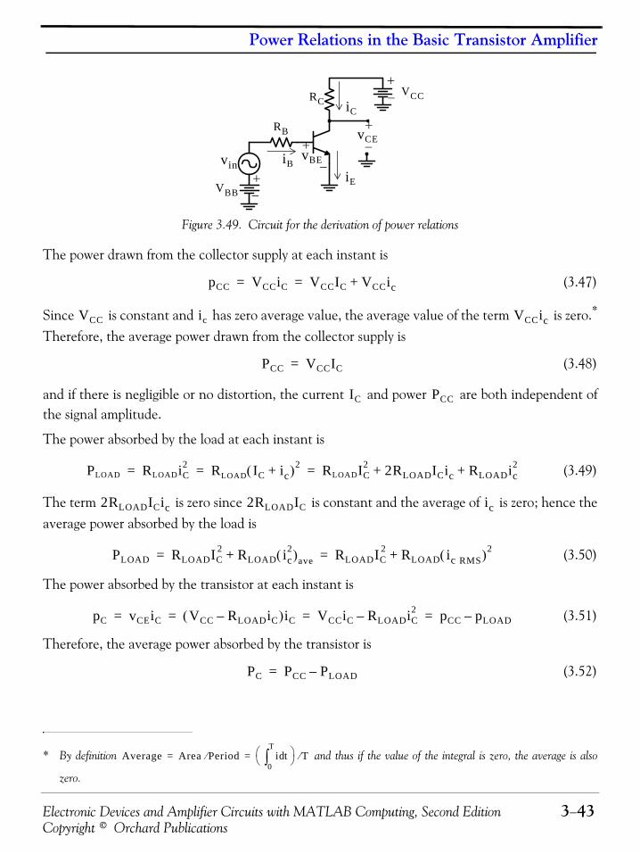
Electronic Devices and Amplifier Circuits with MATLAB Computing, Second Edition 3−43Copyright © Orchard Publications
Power Relations in the Basic Transistor Amplifier
Figure 3.49. Circuit for the derivation of power relations
The power drawn from the collector supply at each instant is
(3.47)
Since is constant and has zero average value, the average value of the term is zero.*
Therefore, the average power drawn from the collector supply is
(3.48)
and if there is negligible or no distortion, the current and power are both independent ofthe signal amplitude.
The power absorbed by the load at each instant is
(3.49)
The term is zero since is constant and the average of is zero; hence theaverage power absorbed by the load is
(3.50)
The power absorbed by the transistor at each instant is
(3.51)
Therefore, the average power absorbed by the transistor is
(3.52)
* By definition and thus if the value of the integral is zero, the average is also
zero.
VCCRC
vBE
+−
vin
iC
VBB
+
−
+
−vCE
iB
RB
+−
iE
pCC VCCiC VCCIC VCCic+= =
VCC ic VCCic
Average Area Period⁄ i td0
T
∫⎝ ⎠⎛ ⎞ T⁄= =
PCC VCCIC=
IC PCC
PLOAD RLOADiC2 RLOAD IC ic+( )2 RLOADIC
2 2RLOADICic RLOADic2+ += = =
2RLOADICic 2RLOADIC ic
PLOAD RLOADIC2 RLOAD ic
2( )ave+ RLOADIC2 RLOAD ic RMS( )2+= =
pC vCEiC VCC RLOADiC–( )iC VCCiC RLOADiC2– pCC pLOAD–= = = =
PC PCC PLOAD–=
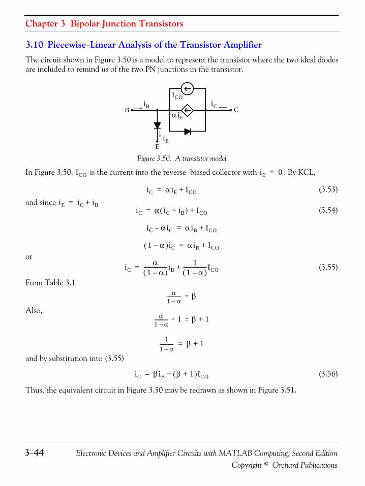
Chapter 3 Bipolar Junction Transistors
3−44 Electronic Devices and Amplifier Circuits with MATLAB Computing, Second EditionCopyright © Orchard Publications
3.10 Piecewise−Linear Analysis of the Transistor AmplifierThe circuit shown in Figure 3.50 is a model to represent the transistor where the two ideal diodesare included to remind us of the two PN junctions in the transistor.
Figure 3.50. A transistor model
In Figure 3.50, is the current into the reverse−biased collector with . By KCL,
(3.53)
and since (3.54)
or(3.55)
From Table 3.1
Also,
and by substitution into (3.55)
(3.56)
Thus, the equivalent circuit in Figure 3.50 may be redrawn as shown in Figure 3.51.
iBBiC
E
C
iE
ICO
αiE
ICO iE 0=
iC αiE ICO+=
iE iC iB+=iC α iC iB+( ) ICO+=
iC αiC– αiB ICO+=
1 α–( )iC αiB ICO+=
iCα
1 α–( )-----------------iB
11 α–( )
-----------------ICO+=
α1 α–------------ β=
α1 α–------------ 1+ β 1+=
11 α–---------- β 1+=
iC βiB β 1+( )ICO+=

Electronic Devices and Amplifier Circuits with MATLAB Computing, Second Edition 3−45Copyright © Orchard Publications
Piecewise−Linear Analysis of the Transistor Amplifier
Figure 3.51. An alternative transistor model.
The transistor models shown in Figures 3.50 and 3.51 are essentially ideal models. An improvedtransistor model is shown in Figure 3.52 where for silicon type of transistors and ,referred to as the base spreading resistance, is included to account for the small voltage drop in thebase of the transistor.
Figure 3.52. A more accurate model for the transistor
Analogous to the base resistance are the emitter diffusion resistance defined as
(3.57)
and the collector resistance
(3.58)
Typical values for are between to , for are between to , and is
very high, in excess of . The model in Figure 3.52 is for an NPN transistors. It applies alsoto PNP transistors provided that the diodes, voltage polarities, and current directions are reversed.
The transistor amplifier in Figure 3.53 can be analyzed by piece−wise linear methods with the aidof the transistor model in Figure 3.52.
iBBiC
E
C
iE
β 1+( )ICO
βiB
VD 0.7 V≈ rb
iBB
iC
E
C
iE
β 1+( )ICO
βiB
VD
rb
rb
re∂vE
∂iE--------
iC cons ttan=
=
rc∂vC
∂iC---------
iE cons ttan=
=
rb 50 Ω 250 Ω re 10 Ω 25 Ω rc
1 MΩ

Chapter 3 Bipolar Junction Transistors
3−46 Electronic Devices and Amplifier Circuits with MATLAB Computing, Second EditionCopyright © Orchard Publications
Figure 3.53. Basic transistor amplifier to be analyzed by piece−wise linear methods
For convenience, we neglect the small effects of , , and in Figure 3.52 and thusthe model is now as shown in Figure 3.54.
Figure 3.54. The piece−wise linear model in Figure 3.52 where , , and are neglected
When the transistor in the amplifier in Figure 3.53 is replaced by the piece−wise linear model inFigure 3.54, we obtain the circuit shown in Figure 3.55(a).
Figure 3.55. Piecewise linear model for the circuit in figure 3.53 and its current transfer characteristics
The current transfer characteristics are constructed by determining the points at which thediodes change from the conducting to the non−conducting state. The current represents thecollector saturation current.
Let us now suppose that the source current reaches a value that causes the reverse voltage
across the collector diode to become zero and the emitter diode is conducting and allows
iSvBE
−
VCC+
+
−
−
+
V1
RC
−vCE+
vS
RS R1
iB
rb VD β 1+( )ICO
iBBiC
E
C
iE
βiB
rb VD β 1+( )ICO
iS
VCC+
−V1
RC
−
vCE+
vS
RS R1
βiB
iE
iC
a( )
Collector diode
short circuited
iC
is
ICSVCC
RC--------=
Emitter diode
open circuited
iS IB–= iSICS
β------ IB–=
b( )
DC
DE
IB
B
E
C
ICS
is
DC DE
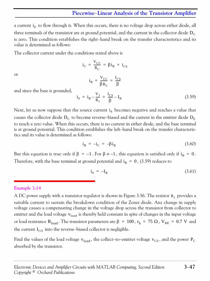
Electronic Devices and Amplifier Circuits with MATLAB Computing, Second Edition 3−47Copyright © Orchard Publications
Piecewise−Linear Analysis of the Transistor Amplifier
a current to flow through it. When this occurs, there is no voltage drop across either diode, all
three terminals of the transistor are at ground potential, and the current in the collector diode is zero. This condition establishes the right−hand break on the transfer characteristics and itsvalue is determined as follows:
The collector current under the conditions stated above is
or
and since the base is grounded,(3.59)
Next, let us now suppose that the source current becomes negative and reaches a value that
causes the collector diode to become reverse−biased and the current in the emitter diode to reach a zero value. When this occurs, there is no current in either diode, and the base terminalis at ground potential. This condition establishes the left−hand break on the transfer characteris-tics and its value is determined as follows:
(3.60)
But this equation is true only if . For , this equation is satisfied only if .
Therefore, with the base terminal at ground potential and , (3.59) reduces to
(3.61)
Example 3.14
A DC power supply with a transistor regulator is shown in Figure 3.56. The resistor provides asuitable current to sustain the breakdown condition of the Zener diode. Any change in supplyvoltage causes a compensating change in the voltage drop across the transistor from collector toemitter and the load voltage is thereby held constant in spite of changes in the input voltage
or load resistance . The transistor parameters are , , and
the current into the reverse−biased collector is negligible.
Find the values of the load voltage , the collect−to−emitter voltage , and the power absorbed by the transistor.
iE
DC
iCVCCRC
--------- βiB ICS= = =
iBVCC
βRC---------
ICS
β-------= =
iS iBV1R1-----–
ICS
β------- IB–= =
iS
DC DE
iB iC– βiB–= =
β 1–= β 1–≠ iB 0=
iB 0=
iS IB–=
R1
vload
Rload β 100= rb 75 Ω= VBE 0.7 V=
ICO
vload vCE PC
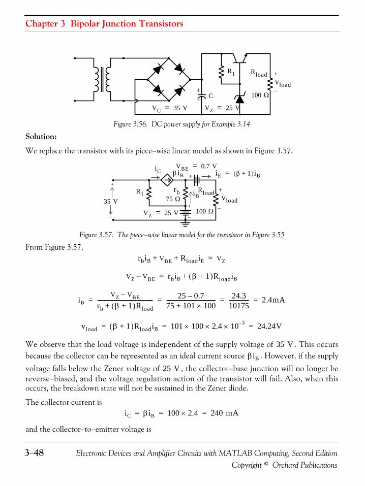
Chapter 3 Bipolar Junction Transistors
3−48 Electronic Devices and Amplifier Circuits with MATLAB Computing, Second EditionCopyright © Orchard Publications
Figure 3.56. DC power supply for Example 3.14
Solution:
We replace the transistor with its piece−wise linear model as shown in Figure 3.57.
Figure 3.57. The piece−wise linear model for the transistor in Figure 3.55
From Figure 3.57,
We observe that the load voltage is independent of the supply voltage of . This occursbecause the collector can be represented as an ideal current source . However, if the supply
voltage falls below the Zener voltage of , the collector−base junction will no longer bereverse−biased, and the voltage regulation action of the transistor will fail. Also, when thisoccurs, the breakdown state will not be sustained in the Zener diode.
The collector current is
and the collector−to−emitter voltage is
vload
+
−C−
+
VC 35 V=
R1 Rload
VZ 25 V=
100 Ω
vload35 VR1
Rload
VZ 25 V= 100 Ω
VBE 0.7 V=
rb75 Ω
iC βiB
iB
iE β 1+( )iB=
−
+
+
+
+
− −
−
rbiB VBE RloadiE+ + VZ=
VZ VBE– rbiB β 1+( )RloadiB+=
iBVZ VBE–
rb β 1+( )Rload+----------------------------------------- 25 0.7–
75 101 100×+------------------------------------ 24.3
10175--------------- 2.4mA= = = =
vload β 1+( )RloadiB 101 100 2.4 10 3–××× 24.24V= = =
35 VβiB
25 V
iC βiB 100 2.4× 240 mA= = =

Electronic Devices and Amplifier Circuits with MATLAB Computing, Second Edition 3−49Copyright © Orchard Publications
Incremental Linear Models
The power absorbed by the transistor is
3.11 Incremental Linear ModelsIn our discussion on piece−wise linear models on the preceding section, the small voltage dropbetween base and emitter is small in comparison with the bias voltage and thus can be neglected.However, the base−to−emitter voltage cannot be neglected when only the increments of voltageand currents is considered. Also, when calculating increments of current and voltage, it is oftennecessary to account for the small effects of variations in collector voltage on both the input andoutput circuits. For these reasons the incremental model for the transistor provides a betterapproximation than the piece−wise linear approximation.
The base−to−emitter voltage and the collector current are functions of the base current
and collector−to−emitter voltage . In other words,
(3.62)and
(3.63)
If and are changed in small increments, the resulting increment in can be expressedas
(3.64)
and the increment in can be written as
(3.65)
The partial derivative in the first term of (3.64) has the dimensions of resistance and it is denotedas , and that in the second term is a dimensionless voltage ratio denoted as . It is also conve-nient to denote these derivatives in lower case letters with lower case subscripts. Then, (3.64) isexpressed as
(3.66)
Likewise, the partial derivative in the first term of (3.65) is a dimensionless current ratio denotedas , and that in the second term has the dimensions of conductance and it is denoted as .Then, (3.65) is expressed as
vCE Supply Voltage Load Voltage– 35 24.24– 10.76 V= = =
PC vCEiC 10.76 0.24× 2.58 w= = =
vBE iC iB
vCE
vBE f iB vCE,( )=
iC f iB vCE,( )=
iB vCE vBE
ΔvBE dvBE≈∂vBE
∂iB-----------diB
∂vBE
∂vCE-----------dvCE+=
iC
ΔiC diC≈∂iC
∂iB-------diB
∂iC
∂vCE-----------dvCE+=
rn μ
vbe rnib μvce+=
β go
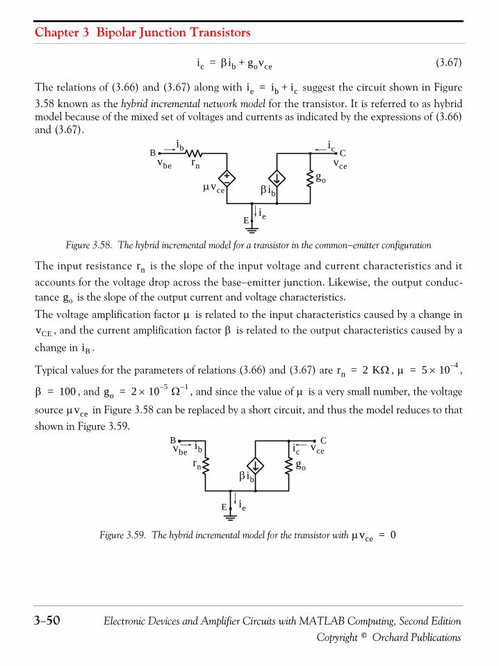
Chapter 3 Bipolar Junction Transistors
3−50 Electronic Devices and Amplifier Circuits with MATLAB Computing, Second EditionCopyright © Orchard Publications
(3.67)
The relations of (3.66) and (3.67) along with suggest the circuit shown in Figure3.58 known as the hybrid incremental network model for the transistor. It is referred to as hybridmodel because of the mixed set of voltages and currents as indicated by the expressions of (3.66)and (3.67).
Figure 3.58. The hybrid incremental model for a transistor in the common−emitter configuration
The input resistance is the slope of the input voltage and current characteristics and itaccounts for the voltage drop across the base−emitter junction. Likewise, the output conduc-tance is the slope of the output current and voltage characteristics.
The voltage amplification factor is related to the input characteristics caused by a change in, and the current amplification factor is related to the output characteristics caused by a
change in .
Typical values for the parameters of relations (3.66) and (3.67) are , ,
, and , and since the value of is a very small number, the voltage
source in Figure 3.58 can be replaced by a short circuit, and thus the model reduces to thatshown in Figure 3.59.
Figure 3.59. The hybrid incremental model for the transistor with
ic βib govce+=
ie ib ic+=
μvce
rnB
ib
vbego
βib
E
ic
vceC
ie
rn
go
μvCE β
iB
rn 2 KΩ= μ 5 10 4–×=
β 100= go 2 10 5– Ω 1–×= μ
μvce
rn
B ibvbego
βib
E
ic vceC
ie
μvce 0=
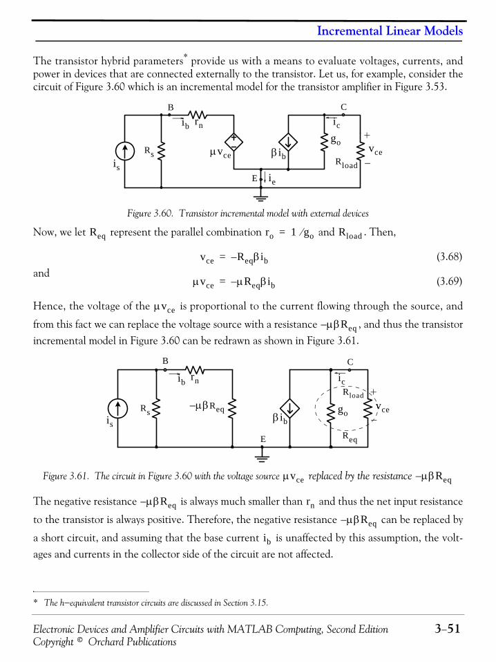
Electronic Devices and Amplifier Circuits with MATLAB Computing, Second Edition 3−51Copyright © Orchard Publications
Incremental Linear Models
The transistor hybrid parameters* provide us with a means to evaluate voltages, currents, andpower in devices that are connected externally to the transistor. Let us, for example, consider thecircuit of Figure 3.60 which is an incremental model for the transistor amplifier in Figure 3.53.
Figure 3.60. Transistor incremental model with external devices
Now, we let represent the parallel combination and . Then,
(3.68)and
(3.69)
Hence, the voltage of the is proportional to the current flowing through the source, and
from this fact we can replace the voltage source with a resistance , and thus the transistorincremental model in Figure 3.60 can be redrawn as shown in Figure 3.61.
Figure 3.61. The circuit in Figure 3.60 with the voltage source replaced by the resistance
The negative resistance is always much smaller than and thus the net input resistance
to the transistor is always positive. Therefore, the negative resistance can be replaced by
a short circuit, and assuming that the base current is unaffected by this assumption, the volt-ages and currents in the collector side of the circuit are not affected.
* The h−equivalent transistor circuits are discussed in Section 3.15.
μvce
rn
B
ib
is
goβib
E
ic
C
ie
Rload
Rs vce
Req ro 1 go⁄= Rload
vce Reqβib–=
μvce μReqβib–=
μvce
μβReq–
μβReq–
rn
B
ib
is
goβib
E
ic
C
Rload
Rsvce
Req
μvce μβReq–
μβReq– rn
μβReq–
ib
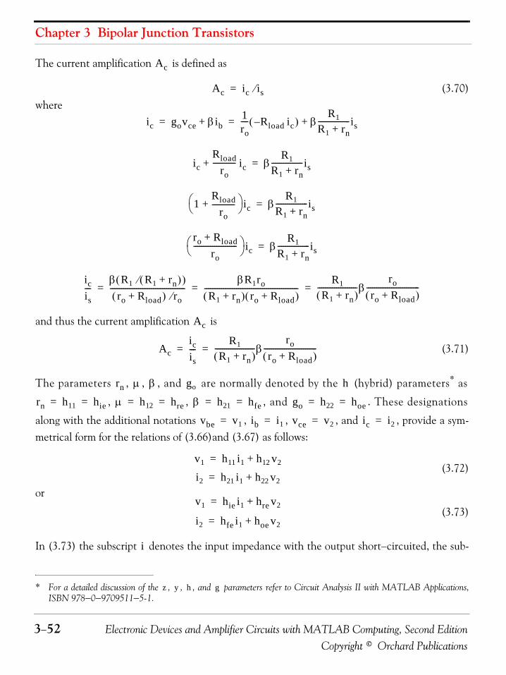
Chapter 3 Bipolar Junction Transistors
3−52 Electronic Devices and Amplifier Circuits with MATLAB Computing, Second EditionCopyright © Orchard Publications
The current amplification is defined as
(3.70)where
and thus the current amplification is
(3.71)
The parameters , , , and are normally denoted by the (hybrid) parameters* as
, , , and . These designations
along with the additional notations , , , and , provide a sym-metrical form for the relations of (3.66)and (3.67) as follows:
(3.72)
or
(3.73)
In (3.73) the subscript denotes the input impedance with the output short−circuited, the sub-
* For a detailed discussion of the , , , and parameters refer to Circuit Analysis II with MATLAB Applications,ISBN 978−0−9709511−5-1.
Ac
Ac ic is⁄=
ic govce βib+1ro---- Rload ic–( ) β
R1
R1 rn+-----------------is+= =
icRload
ro------------ ic+ β
R1
R1 rn+-----------------is=
1Rload
ro------------+⎝ ⎠
⎛ ⎞ ic βR1
R1 rn+-----------------is=
ro Rload+
ro-----------------------⎝ ⎠
⎛ ⎞ ic βR1
R1 rn+-----------------is=
icis---
β R1 R1 rn+( )⁄( )ro Rload+( ) ro⁄
----------------------------------------βR1ro
R1 rn+( ) ro Rload+( )--------------------------------------------------
R1
R1 rn+( )---------------------β
roro Rload+( )
----------------------------= = =
Ac
Acicis---
R1
R1 rn+( )---------------------β
roro Rload+( )
----------------------------= =
rn μ β go h
z y h g
rn h11 hie= = μ h12 hre= = β h21 hfe= = go h22 hoe= =
vbe v1= ib i1= vce v2= ic i2=
v1 h11 i1 h12 v2+=
i2 h21 i1 h22 v2+=
v1 hie i1 hre v2+=
i2 hfe i1 hoe v2+=
i

Electronic Devices and Amplifier Circuits with MATLAB Computing, Second Edition 3−53Copyright © Orchard Publications
Incremental Linear Models
script denotes the reverse transfer voltage ratio with the input terminals open−circuited, thesubscript denotes the forward transfer current ratio with the output short circuited, and the sub-script denotes the output admittance with the input terminals open−circuited. The second sub-script indicates that the parameters apply for the transistor operating in the common−emittermode. A similar set of symbols with the subscript replacing the subscript denotes the hybridparameters for a transistor operating in the common−base mode, and a set with the subscript replacing the letter denotes the hybrid parameters for a transistor operating in the common−col-lector mode.
Values for the hybrid parameters at a typical quiescent operating point for the common−emittermode are provided by the transistor manufacturers. Please refer to the last section in this chapter.Table 3.3 lists the h−parameter equations for the three bipolar transistor configurations.
Example 3.15
For the amplifier circuit in Figure 3.62 it is known that , ,
, and . Find the small signal current amplification
.
Figure 3.62. Transistor amplifier for Example 3.15Solution:The incremental model of this transistor amplifier is shown in Figure 3.63 where
TABLE 3.3 h−parameter equations for transistorsParameter Common−Base Common−Emitter Common−Collector
rf
oe
b ec
e
h11 hib hie h11 1 h21+( )⁄≈ hic h11 1 h21+( )⁄≈
h12 hrb hre h11h22 1 h21+( )⁄ h12–≈ hrc 1≈
h21 hfb hfe h21 1 h21+( )⁄–≈ hfc 1 1 h21+( )⁄–≈
h22 hob hoe h22 1 h21+( )⁄≈ hoc h22 1 h21+( )⁄≈
rn h11 2 KΩ= = β h21 100= =
μ h12 5 10 4–×= = go h22 2 10 5–× Ω 1–= =
Ac iload is⁄=
is
+
−
−+
2 KΩ
vs
Rs
iload
10 KΩ16 V
2 V
R1
RC
VCC
+
−
vCE
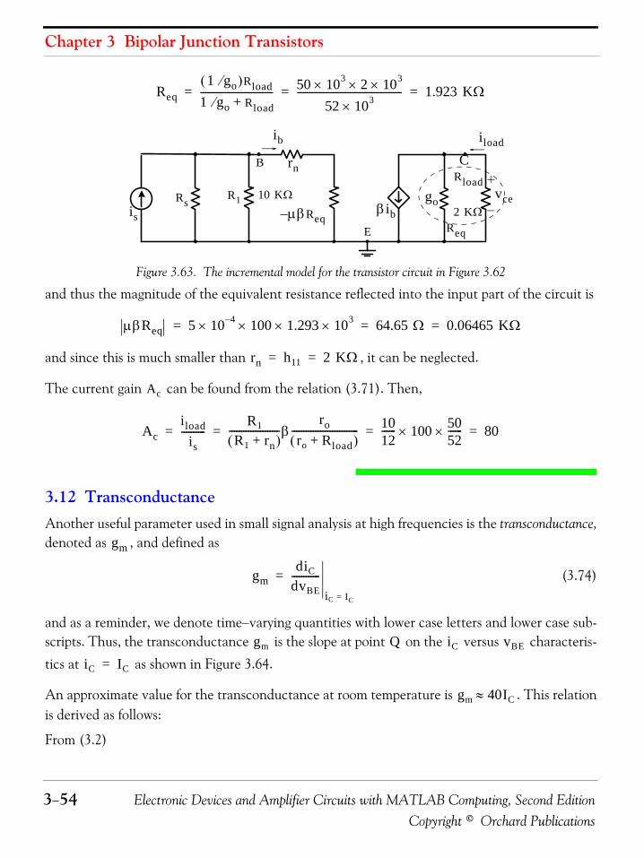
Chapter 3 Bipolar Junction Transistors
3−54 Electronic Devices and Amplifier Circuits with MATLAB Computing, Second EditionCopyright © Orchard Publications
Figure 3.63. The incremental model for the transistor circuit in Figure 3.62
and thus the magnitude of the equivalent resistance reflected into the input part of the circuit is
and since this is much smaller than , it can be neglected.
The current gain can be found from the relation (3.71). Then,
3.12 TransconductanceAnother useful parameter used in small signal analysis at high frequencies is the transconductance,denoted as , and defined as
(3.74)
and as a reminder, we denote time−varying quantities with lower case letters and lower case sub-scripts. Thus, the transconductance is the slope at point on the versus characteris-
tics at as shown in Figure 3.64.
An approximate value for the transconductance at room temperature is . This relationis derived as follows:
From (3.2)
Req1 go⁄( )Rload
1 go⁄ Rload+------------------------------ 50 103× 2 103××
52 103×-------------------------------------------- 1.923 KΩ= = =
μβReq–
rnB
ib
is
goβib
E
iload
CRload
R1 vce
Req
Rs10 KΩ
2 KΩ
μβReq 5 10 4–× 100× 1.293 103×× 64.65 Ω 0.06465 KΩ= = =
rn h11 2 KΩ= =
Ac
Aciload
is----------
R1
R1 rn+( )---------------------β
roro Rload+( )
---------------------------- 1012------ 100 50
52------×× 80= = = =
gm
gmdiC
dvBE------------
iC IC=
=
gm Q iC vBE
iC IC=
gm 40IC≈
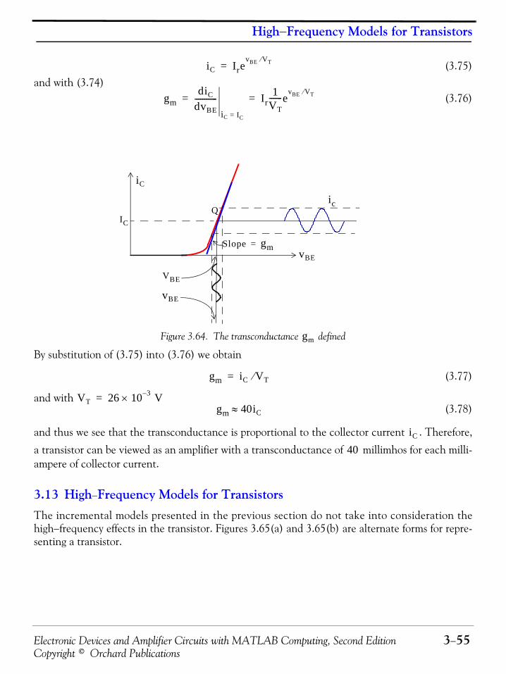
Electronic Devices and Amplifier Circuits with MATLAB Computing, Second Edition 3−55Copyright © Orchard Publications
High−Frequency Models for Transistors
(3.75)and with (3.74)
(3.76)
Figure 3.64. The transconductance defined
By substitution of (3.75) into (3.76) we obtain
(3.77)
and with (3.78)
and thus we see that the transconductance is proportional to the collector current . Therefore,
a transistor can be viewed as an amplifier with a transconductance of millimhos for each milli-ampere of collector current.
3.13 High−Frequency Models for TransistorsThe incremental models presented in the previous section do not take into consideration thehigh−frequency effects in the transistor. Figures 3.65(a) and 3.65(b) are alternate forms for repre-senting a transistor.
iC IrevBE VT⁄
=
gmdiC
dvBE------------
iC IC=
Ir1
VT-------e
vBE VT⁄= =
iC
vBE
QIC
VBE
Slope gm=
vBE
ic
gm
gm iC VT⁄=
VT 26 10 3– V×=gm 40iC≈
iC
40

Chapter 3 Bipolar Junction Transistors
3−56 Electronic Devices and Amplifier Circuits with MATLAB Computing, Second EditionCopyright © Orchard Publications
Figure 3.65. Alternate forms for the transistor model
In Figure 3.65(a) the input impedance is separated into two parts; one part, denoted as ,
accounts for the ohmic base spreading resistance; the other part, denoted as , is a nonlinear
resistance and accounts for the voltage drop across the emitter junction. Thus,
(3.79)
From Figure 3.65(a)(3.80)
and thus* (3.81)
and thus the model in Figure 3.65(a) can also be represented as that in Figure 3.65(b).
From (3.76)(3.82)
or(3.83)
Thus, when , , and in general, when is in milliamps,
(3.84)
The incremental models we have discussed thus far are valid only for frequencies of about or less. For higher frequencies, the effects of junction capacitances must be taken into
account. Figure 3.66 shows a model for the transistor at high frequencies referred to as hybrid−model.
* Since , it follows that
rbe
Bib
vbero
βibE
icvce
C
ie
r'b
v'be
rbe
ib
vbero
gmv'be
icvcer'b
v'be
b( )a( )
B C
E ie
rn r'brbe
v'be
rn r'b rbe+=
ibv'berbe--------=
βibβ
rbe------v'be gmv'be= =
ic βib βv 'berbe-----------= =
icv 'be-----------
vce 0=
dicdv 'be--------------
vCE cons ttan=
gm= =
gm β rbe⁄=
rbeβ
gm------ β
40iC----------= =
iC 1 ma= rbe 25β Ω= iC
rbe 25β( ) iC⁄=
2 MHzπ
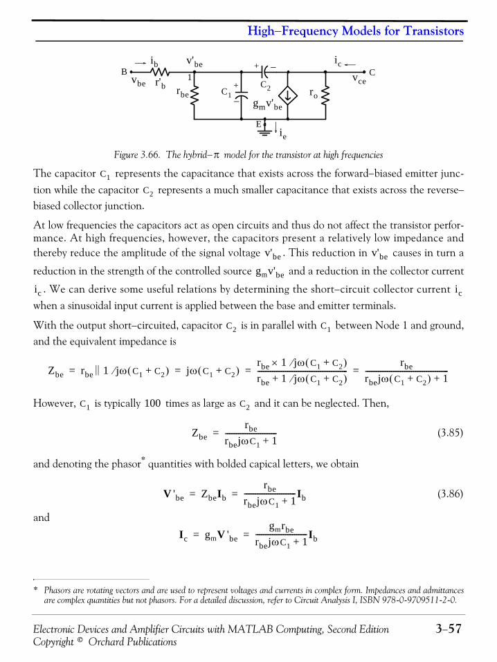
Electronic Devices and Amplifier Circuits with MATLAB Computing, Second Edition 3−57Copyright © Orchard Publications
High−Frequency Models for Transistors
Figure 3.66. The hybrid− model for the transistor at high frequencies
The capacitor represents the capacitance that exists across the forward−biased emitter junc-tion while the capacitor represents a much smaller capacitance that exists across the reverse−biased collector junction.
At low frequencies the capacitors act as open circuits and thus do not affect the transistor perfor-mance. At high frequencies, however, the capacitors present a relatively low impedance andthereby reduce the amplitude of the signal voltage . This reduction in causes in turn a
reduction in the strength of the controlled source and a reduction in the collector current
. We can derive some useful relations by determining the short−circuit collector current when a sinusoidal input current is applied between the base and emitter terminals.
With the output short−circuited, capacitor is in parallel with between Node 1 and ground,and the equivalent impedance is
However, is typically times as large as and it can be neglected. Then,
(3.85)
and denoting the phasor* quantities with bolded capical letters, we obtain
(3.86)
and
* Phasors are rotating vectors and are used to represent voltages and currents in complex form. Impedances and admittancesare complex quantities but not phasors. For a detailed discussion, refer to Circuit Analysis I, ISBN 978-0-9709511-2-0.
rbe
Bib
vbero
gmv'be
E
ic
vceC
ie
r'b
v'be
+
−
C1C2
1+
−
π
C1
C2
v'be v'be
gmv'be
ic ic
C2 C1
Zbe rbe 1 jω C1 C2+( )⁄|| jω C1 C2+( )rbe 1 jω C1 C2+( )⁄×rbe 1 jω C1 C2+( )⁄+-------------------------------------------------
rberbejω C1 C2+( ) 1+---------------------------------------------= = = =
C1 100 C2
Zberbe
rbejωC1 1+----------------------------=
V 'be ZbeIbrbe
rbejωC1 1+----------------------------Ib= =
Ic gmV 'begmrbe
rbejωC1 1+----------------------------Ib= =

Chapter 3 Bipolar Junction Transistors
3−58 Electronic Devices and Amplifier Circuits with MATLAB Computing, Second EditionCopyright © Orchard Publications
Using the relation of (3.82) we obtain
(3.87)
Thus, if the amplitude of the input current is held constant as the frequency is increased, theamplitude of the collector current decreases and approaches zero at very high frequencies.
The coefficient of in (3.86) must be a dimensionless constant; therefore the quantity
has the dimensions of frequency. Also, it is customary to represent as , and it is helpful to
define a new symbol as
(3.88)
By substitution of (3.88) into (3.87) we obtain
(3.89)
and the magnitute of the collector current is
(3.90)
Therefore, at the frequency , the magnitude of the collector current is reduced to
times its low−frequency value. Thus, serves as a useful measure of the band of fre-quencies over which the short−circuit current amplification remains reasonably constant andnearly equal to its low−frequency value. For this reason, is referred to as the cutoff fre-quency.
The frequency at which the current amplification is unity, that is, the frequency at which, is found from (3.90) as
(3.91)
As we know, a typical value for is ; therefore, in (3.91) the term is much larger
than unity and . Letting , we obtain
(3.92)
The relation of (3.92) is referred to as the current gain−bandwidth product for the transistor and
Icβ
rbejωC1 1+----------------------------Ib=
Ib 1 rbeC1⁄
C1 Ce
ωβ
ωβ1
rbeCe-------------≡
Icβ
jω ωβ⁄ 1+-------------------------- Ib=
Icβ
ω ωβ⁄( )2 1+----------------------------------- Ib=
ω ωβ= Ic
1 2⁄ ωβ
ωβ β
Ic Ib=
β ω ωβ⁄( )2 1+=
β 100 ω ωβ⁄( )2
ω ωβ» ω ωT=
ωT βωβ≈ fT βfβ≈

Electronic Devices and Amplifier Circuits with MATLAB Computing, Second Edition 3−59Copyright © Orchard Publications
High−Frequency Models for Transistors
it is an important figure of merit* for a transistor. Also, from (3.82), (3.88), and (3.92)
(3.93)
or(3.94)
Example 3.16
The specifications for a certain transistor state that , the current gain−bandwidth prod-uct is , and the collector current is . Using the hybrid− model of Fig-ure 3.66, find:
a. the transconductance
b. the base−emitter capacitance
c. the base−emitter resistance
d. the cutoff frequency
Solution:
a. From (3.78)
b. From (3.94)
c. From (3.83)
d. From (3.92)
and this indicates that at this frequency the current amplification is still large.
* The figure of merit is useful in comparing different devices for their overall performance.
ωTgmCe------=
fTgm
2πCe-------------=
β 100=
fT 200 MHz= iC 1 mA= π
gm
Ce
rbe
β
gm 40iC 40 millimhos=≈
Cegm
2πfT----------- 40 10 3–×
2π 2 108××------------------------------ 32 pF≈= =
rbeβ
gm------ 100
40 10 3–×---------------------- 2.5 KΩ= = =
fβfT
β---- 200 106×
100----------------------- 2 MHz= = =
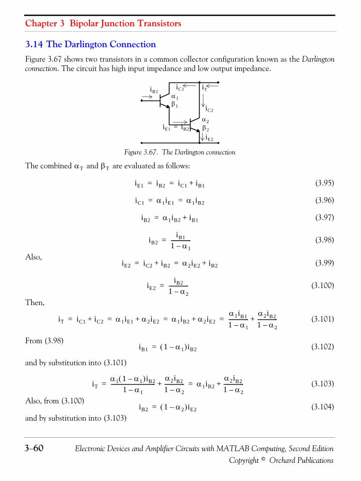
Chapter 3 Bipolar Junction Transistors
3−60 Electronic Devices and Amplifier Circuits with MATLAB Computing, Second EditionCopyright © Orchard Publications
3.14 The Darlington ConnectionFigure 3.67 shows two transistors in a common collector configuration known as the Darlingtonconnection. The circuit has high input impedance and low output impedance.
Figure 3.67. The Darlington connection
The combined and are evaluated as follows:
(3.95)
(3.96)
(3.97)
(3.98)
Also,(3.99)
(3.100)
Then,
(3.101)
From (3.98)(3.102)
and by substitution into (3.101)
(3.103)
Also, from (3.100)(3.104)
and by substitution into (3.103)
iTα1
iC2
iC1iB1
iE1 iB2=
iE2
α2
β1
β2
αT βT
iE1 iB2 iC1 iB1+= =
iC1 α1iE1 α1iB2= =
iB2 α1iB2 iB1+=
iB2iB1
1 α1–---------------=
iE2 iC2 iB2+ α2iE2 iB2+= =
iE2iB2
1 α2–---------------=
iT iC1 iC2+ α1iE1 α2iE2+ α1iB2 α2iE2+α1iB1
1 α1–---------------
α2iB2
1 α2–---------------+= = = =
iB1 1 α1–( )iB2=
iTα1 1 α1–( )iB2
1 α1–---------------------------------
α2iB2
1 α2–---------------+ α1iB2
α2iB2
1 α2–---------------+= =
iB2 1 α2–( )iE2=
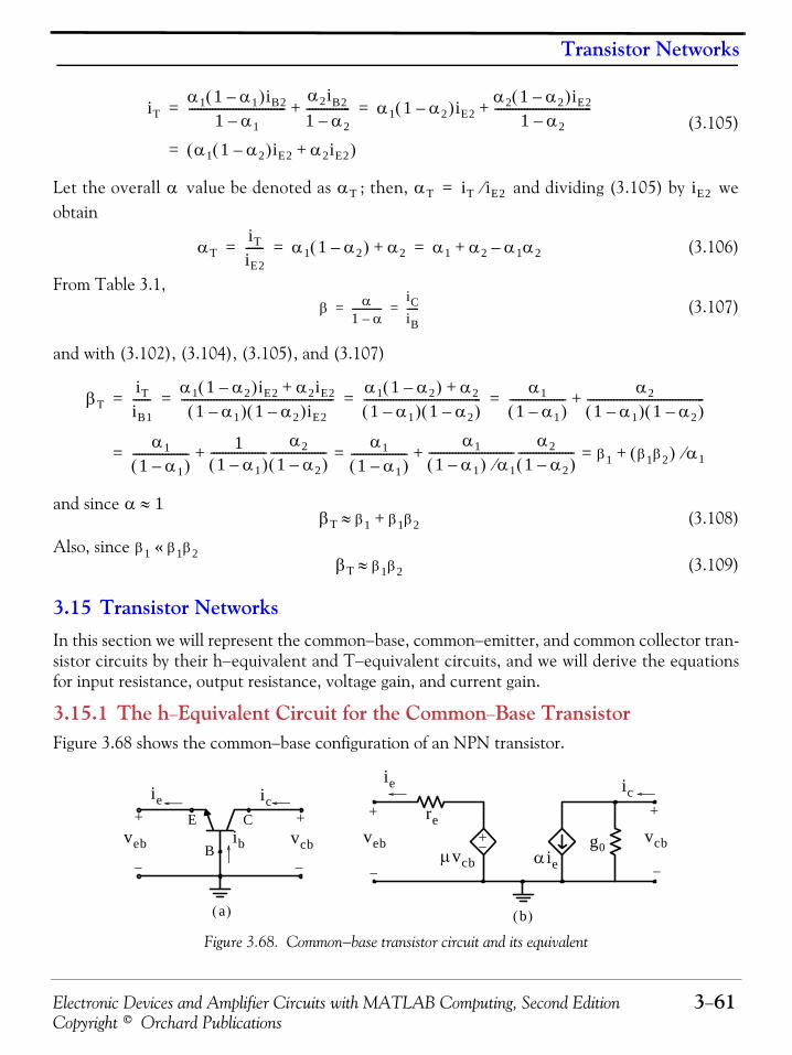
Electronic Devices and Amplifier Circuits with MATLAB Computing, Second Edition 3−61Copyright © Orchard Publications
Transistor Networks
(3.105)
Let the overall value be denoted as ; then, and dividing (3.105) by weobtain
(3.106)
From Table 3.1,(3.107)
and with (3.102), (3.104), (3.105), and (3.107)
and since (3.108)
Also, since (3.109)
3.15 Transistor NetworksIn this section we will represent the common−base, common−emitter, and common collector tran-sistor circuits by their h−equivalent and T−equivalent circuits, and we will derive the equationsfor input resistance, output resistance, voltage gain, and current gain.
3.15.1 The h−Equivalent Circuit for the Common−Base TransistorFigure 3.68 shows the common−base configuration of an NPN transistor.
Figure 3.68. Common−base transistor circuit and its equivalent
iTα1 1 α1–( )iB2
1 α1–---------------------------------
α2iB2
1 α2–---------------+ α1 1 α2–( )iE2
α2 1 α2–( )iE2
1 α2–---------------------------------+= =
α1 1 α2–( )iE2 α2iE2+( )=
α αT αT iT iE2⁄= iE2
αTiT
iE2------ α1 1 α2–( ) α2+ α1 α2 α1α2–+= = =
β α1 α–------------
iCiB-----= =
βTiT
iB1------ α1 1 α2–( )iE2 α2iE2+
1 α1–( ) 1 α2–( )iE2---------------------------------------------------- α1 1 α2–( ) α2+
1 α1–( ) 1 α2–( )---------------------------------------- α1
1 α1–( )------------------- α2
1 α1–( ) 1 α2–( )----------------------------------------+= = = =
α1
1 α1–( )------------------- 1
1 α1–( )------------------- α2
1 α2–( )-------------------+
α1
1 α1–( )-------------------
α1
1 α1–( ) α1⁄----------------------------- α2
1 α2–( )-------------------+ β1 β1β2( ) α1⁄+= ==
α 1≈βT β1 β1β2+≈
β1 β1β2«βT β1β2≈
E C
B
ie
veb ib
ic
vcb vcbg0αie
reveb
ie ic
μvcb
a( ) b( )

Chapter 3 Bipolar Junction Transistors
3−62 Electronic Devices and Amplifier Circuits with MATLAB Computing, Second EditionCopyright © Orchard Publications
From the equivalent circuit in Figure 3.68(b) we can draw the h−parameter equivalent circuitshown in Figure 3.69.
Figure 3.69. The h−parameter equivalent circuit for common−base transistor
From Figures 3.68 and (3.69), se observe that
Typical values for the h−parameter equivalent circuit for the common−base transistor are:
As indicated above, the input resistance has a small value, typically in the to .This can be shown as follows:
From (3.2)(3.110)
or(3.111)
and since (3.112)
by substitution of (3.112) into (3.111) we obtain
(3.113)
Normally, and we recall that
Retaining only the first two terms of this series, by substitution into (3.113) we obtain
(3.114)
vcbhobhfbie
hib
hrbvcb
veb
hib re= hob go= hfb α= hrb μ=
hib 30 Ω= hrb 5 10 4–×= hfb 0.98= hob 6 10 6– Ω 1–×=
hib re= 25 35 Ω
iC IrevBE VT⁄
=
iC IC ic+ IrevBE vbe+( ) VT⁄
IrevBE VT⁄
evbe VT⁄
⋅= = =
IC IrevBE VT⁄
=
iC ICevbe VT⁄
=
vbe VT«
ex 1 x x2
2!----- x3
3!----- x4
4!----- …+ + + + +=
iC IC 1vbeVT-------+⎝ ⎠
⎛ ⎞ ICIC
VT-------vbe+= =
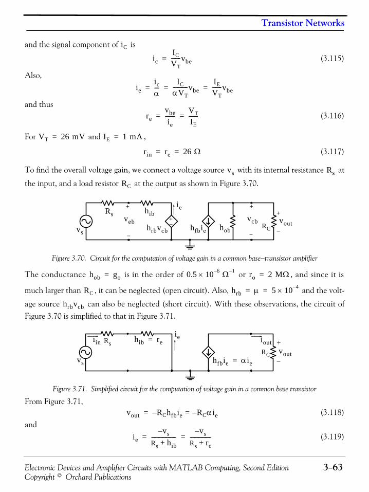
Electronic Devices and Amplifier Circuits with MATLAB Computing, Second Edition 3−63Copyright © Orchard Publications
Transistor Networks
and the signal component of is
(3.115)
Also,
and thus(3.116)
For and ,
(3.117)
To find the overall voltage gain, we connect a voltage source with its internal resistance at
the input, and a load resistor at the output as shown in Figure 3.70.
Figure 3.70. Circuit for the computation of voltage gain in a common base−transistor amplifier
The conductance is in the order of or , and since it is
much larger than , it can be neglected (open circuit). Also, and the volt-
age source can also be neglected (short circuit). With these observations, the circuit ofFigure 3.70 is simplified to that in Figure 3.71.
Figure 3.71. Simplified circuit for the computation of voltage gain in a common base transistor
From Figure 3.71,(3.118)
and(3.119)
iC
icIC
VT-------vbe=
ieicα---
IC
αVT-----------vbe
IE
VT-------vbe= = =
revbeie
------- VT
IE-------= =
VT 26 mV= IE 1 mA=
rin re 26 Ω= =
vs Rs
RC
vcbhobhfbie
hib
hrbvcb
vebRC
Rs
vs
vout
ie
hob go= 0.5 10 6–× Ω 1– ro 2 MΩ=
RC hrb μ 5 10 4–×= =
hrbvcb
hfbie αie=
hib re=
RC
Rs
vs
vout
ie ioutiin
vout RChfbie RCαie–=–=
ievs–
Rs hib+------------------
vs–
Rs re+---------------= =

Chapter 3 Bipolar Junction Transistors
3−64 Electronic Devices and Amplifier Circuits with MATLAB Computing, Second EditionCopyright © Orchard Publications
Substitution of (3.119) into (3.118) and division by yields the overall voltage gain as
(3.120)
and since and , the voltage gain depends on the values of and .
The current gain is
(3.121)
and the output resistance is(3.122)
Example 3.17
An NPN transistor is connected in a common−base configuration with ,
, , , and . Find the voltage and current gains,and input and output resistances.Solution:
3.15.2 The T−Equivalent Circuit for the Common−Base TransistorTransistor equivalent circuits can also be expressed as T−equivalent circuits. Figure 3.72 showsthe common−base T−equivalent circuit.
vs Av
Avvoutvs
--------- αRC
Rs re+---------------= =
α 1≈ re 26Ω≈ Rs RC
Ai
Aiioutiin--------
αie–
ie–----------- α= = =
RoutRout RC=
VT 26 mV=
iE 1 mA= β 120= RS 2 KΩ= RC 5 KΩ=
α ββ 1+------------ 120
121--------- 0.992= = =
hib re VT iE⁄ 26 mV 1 mA⁄ 26 Ω= = = =
AVαRC
Rs re+--------------- 0.992 5 103××
2 0.026+( ) 103×------------------------------------------ 2.45= = =
Ai α 0.992= =
Ri re 26 Ω= =
Ro RC 5 KΩ= =

Electronic Devices and Amplifier Circuits with MATLAB Computing, Second Edition 3−65Copyright © Orchard Publications
Transistor Networks
Figure 3.72. T−equivalent model for the common−base transistor
Typical numerical values for the 2N525 transistor are as follows:
and since
and with these assumptions the input and output resistances and voltage and current gains for theT−equivalent model for the common−base transistor are:
(3.123)
(3.124)
(3.125)
(3.126)
3.15.3 The h−Equivalent Circuit for the Common−Emitter TransistorFigure 3.73 shows the common−emitter configuration of an NPN transistor.
re
ie
rb
rc
αie ic
vs
RsRL
ib
α 0.978=
rc 1.67 MΩ=
re 12.5 Ω=
rb 840 Ω=
re rc«
rb rc«
RL rc<
Input resis cetan rin re rb 1 α–( )+= =
Output resis cetan rout rere rb 1 α–( ) RS+ +
re rb RS+ +---------------------------------------------⋅= =
Voltage gain AvαRL
re rb 1 α–( )+---------------------------------= =
Current gain Ai α= =
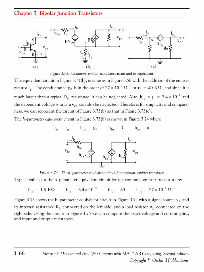
Chapter 3 Bipolar Junction Transistors
3−66 Electronic Devices and Amplifier Circuits with MATLAB Computing, Second EditionCopyright © Orchard Publications
Figure 3.73. Common−emitter transistor circuit and its equivalent
The equivalent circuit in Figure 3.73(b), is same as in Figure 3.58 with the addition of the emitter
resistor . The conductance is in the order of or , and since it is
much larger than a typical resistance, it can be neglected. Also, and
the dependent voltage source can also be neglected. Therefore, for simplicity and compact-ness, we can represent the circuit of Figure 3.73(b) as that in Figure 3.73(c).
The h−parameter equivalent circuit in Figure 3.73(b) is shown in Figure 3.74 where
Figure 3.74. The h−parameter equivalent circuit for common−emitter transistor
Typical values for the h−parameter equivalent circuit for the common−emitter transistor are:
Figure 3.75 shows the h−parameter equivalent circuit in Figure 3.74 with a signal source and
its internal resistance connected on the left side, and a load resistor connected on theright side. Using the circuit in Figure 3.75 we can compute the exact voltage and current gains,and input and output resistances.
E
C
B
ib
vbe
ib
ic
vce
vce
g0βib
vbe
ic
c( )b( )
ie
rn
E
C
B
ie
μvce
a( )
rn
ib
βib
icC
vce
re
AA
re g0 27 10 6–× Ω 1– r0 40 KΩ=
RC hre μ 3.4 10 4–×= =
μvce
hie rn= hoe g0= hfe β= hre μ=
vcehoehfeib
hie
hrevce
vbe
ib ic
hie 1.5 KΩ= hre 3.4 10 4–×= hfe 80= hoe 27 10 6– Ω 1–×=
vS
RS RL
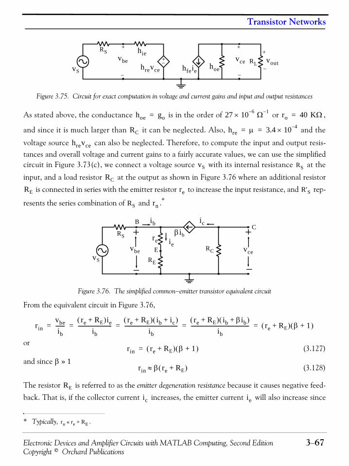
Electronic Devices and Amplifier Circuits with MATLAB Computing, Second Edition 3−67Copyright © Orchard Publications
Transistor Networks
Figure 3.75. Circuit for exact computation in voltage and current gains and input and output resistances
As stated above, the conductance is in the order of or ,
and since it is much larger than it can be neglected. Also, and the
voltage source can also be neglected. Therefore, to compute the input and output resis-tances and overall voltage and current gains to a fairly accurate values, we can use the simplifiedcircuit in Figure 3.73(c), we connect a voltage source with its internal resistance at the
input, and a load resistor at the output as shown in Figure 3.76 where an additional resistor
is connected in series with the emitter resistor to increase the input resistance, and rep-
resents the series combination of and .*
Figure 3.76. The simplified common−emitter transistor equivalent circuit
From the equivalent circuit in Figure 3.76,
or(3.127)
and since (3.128)
The resistor is referred to as the emitter degeneration resistance because it causes negative feed-
back. That is, if the collector current increases, the emitter current will also increase since
* Typically, .
vcehoehfeie
hie
hrevce
vbe RL
RS
vS
vout
hoe go= 27 10 6–× Ω 1– ro 40 KΩ=
RC hre μ 3.4 10 4–×= =
hrevce
vS RS
RC
RE re R'SRS rn
rn re RE+«
ib
vceRC
βib
vbe
ic
iereE
CB
RE
RS
vS
rinvbeib
-------re RE+( )ie
ib--------------------------
re RE+( ) ib ic+( )ib
-----------------------------------------re RE+( ) ib βib+( )
ib--------------------------------------------- re RE+( ) β 1+( )= = = = =
rin re RE+( ) β 1+( )=
β 1»rin β re RE+( )≈
RE
ic ie
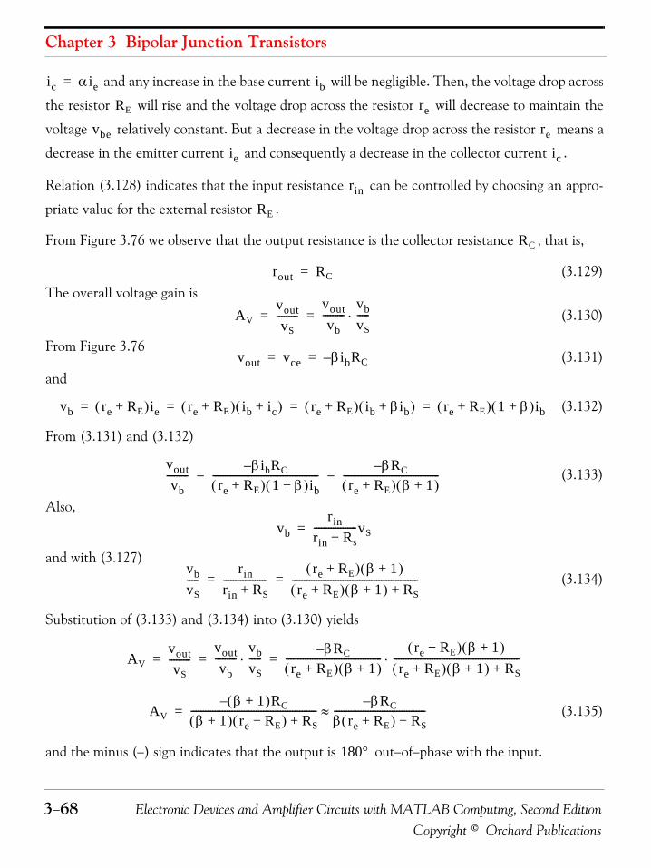
Chapter 3 Bipolar Junction Transistors
3−68 Electronic Devices and Amplifier Circuits with MATLAB Computing, Second EditionCopyright © Orchard Publications
and any increase in the base current will be negligible. Then, the voltage drop across
the resistor will rise and the voltage drop across the resistor will decrease to maintain the
voltage relatively constant. But a decrease in the voltage drop across the resistor means a
decrease in the emitter current and consequently a decrease in the collector current .
Relation (3.128) indicates that the input resistance can be controlled by choosing an appro-
priate value for the external resistor .
From Figure 3.76 we observe that the output resistance is the collector resistance , that is,
(3.129)The overall voltage gain is
(3.130)
From Figure 3.76(3.131)
and
(3.132)
From (3.131) and (3.132)
(3.133)
Also,
and with (3.127)(3.134)
Substitution of (3.133) and (3.134) into (3.130) yields
(3.135)
and the minus (−) sign indicates that the output is out−of−phase with the input.
ic αie= ib
RE re
vbe re
ie ic
rin
RE
RC
rout RC=
AVvoutvS
---------voutvb
---------vbvS-----⋅= =
vout vce βibRC–= =
vb re RE+( )ie re RE+( ) ib ic+( ) re RE+( ) ib βib+( ) re RE+( ) 1 β+( )ib= = = =
voutvb
--------- βibRC–re RE+( ) 1 β+( )ib
-------------------------------------------- βRC–re RE+( ) β 1+( )
----------------------------------------= =
vbrin
rin Rs+------------------vS=
vbvS-----
rinrin RS+------------------
re RE+( ) β 1+( )re RE+( ) β 1+( ) RS+
----------------------------------------------------= =
AVvoutvS
---------voutvb
---------vbvS-----⋅
βRC–re RE+( ) β 1+( )
----------------------------------------re RE+( ) β 1+( )
re RE+( ) β 1+( ) RS+----------------------------------------------------⋅= = =
AVβ 1+( )– RC
β 1+( ) re RE+( ) RS+---------------------------------------------------- β– RC
β re RE+( ) RS+--------------------------------------≈=
180°
Electronic Devices and Amplifier Circuits with MATLAB Computing, Second Edition 3−69Copyright © Orchard Publications
Transistor Networks
From (3.134) we observe that the introduction of the external resistor results in reduction ofthe overall gain.
The current gain is
(3.136)
Example 3.18
An NPN transistor is connected in a common−emitter configuration with ,
, , , and .
a. Find the voltage and current gains, and input and output resistances if .
b. Find the voltage and current gains, and input and output resistances if .
c. Find the maximum value of the applied signal so that or under the conditions of (a)
and (b) will not exceed .
Solution:a.
From (3.116)
From (3.128)
and from (3.129)
The voltage and current gains are found from (3.135) and (3.136). Thus, with , thevoltage gain is
and the current gain is
b.
RE
Aiioutib
--------βib–
ib----------- β–= = =
VT 26 mV=
iE 1 mA= β 120= RS 2 KΩ= RC 5 KΩ=
RE 0=
RE 200Ω=
vS vbe vb
5 mV
hie re VT iE⁄ 26 mV 1 mA⁄ 26 Ω= = = =
rin β re RE+( )≈ 120 26 0+( ) 3.12 KΩ= =
rout RC 5 KΩ= =
RE 0=
AVβ– RC
βre Rs+-------------------- 120 5 103××–
120 26 2 103×+×--------------------------------------------- 117.2–= =≈
Ai β– 120–= =
rin β re RE+( )≈ 120 26 200+( ) 27.12 KΩ= =
rout RC 5 KΩ= =
AVβ– RC
β re RE+( ) Rs+------------------------------------- 120 5 103××–
120 26 200+( ) 2 103×+-----------------------------------------------------------=≈ 20.6–=
Chapter 3 Bipolar Junction Transistors
3−70 Electronic Devices and Amplifier Circuits with MATLAB Computing, Second EditionCopyright © Orchard Publications
We observe that whereas the addition of has increased the input resistance by ,
the voltage gain has decreased by .c.
Without ,
and
With ,
Then,
We observe that for an increase of in input resistance, the maximum value of theapplied signal decreases by .
3.15.4 The T−Equivalent Circuit for the Common−Emitter TransistorFigure 3.77 shows the common−emitter T−equivalent circuit.
Figure 3.77. T−equivalent model for the common−emitter transistor
As with the T-equivalent model for the common-base transistor, we assume that
Ai β– 120–= =
RE 88.5%82.4%
RErin βre≈ 120 26× 3.12 KΩ= =
vberin
rin Rs+------------------vS=
vS max( )rin Rs+
rin------------------vbe
3.12 2+3.12
------------------- 5 mV× 8.2 mV= = =
RErin β re RE+( )≈ 120 26 200+( ) 27.12 KΩ= =
vS max( )rin Rs+
rin------------------vbe
27.12 2+27.12
---------------------- 5 mV× 5.4 mV= = =
88.5%vS 51.8%
rb
ib
re
rc
βib ic
vS
RS
RLievbe
B
E
C
re rc«
rb rc«

Electronic Devices and Amplifier Circuits with MATLAB Computing, Second Edition 3−71Copyright © Orchard Publications
Transistor Networks
and with these assumptions the input and output resistances and voltage and current gains for theT−equivalent model for the common−emitter transistor are:
(3.137)
(3.138)
(3.139)
(3.140)
3.15.5 The h−Equivalent Circuit for the Common−Collector TransistorFigure 3.78 shows the common−collector or emitter−follower configuration of an NPN transistor.The emitter−follower is useful in applications where a high−resistance source is to be connected toa low−resistance load.
Figure 3.78. Common−collector or emitter−follower transistor circuit and its equivalent
From the equivalent circuit in Figure 3.78(b) we can draw the h−parameter equivalent circuit shownin Figure 3.79 where
RL rc<
Input resis cetan rin rbre
1 α–------------+= =
Output resis cetan rout rc 1 α–( ) reαrc RS+
re rb RS+ +---------------------------⋅+= =
Voltage gain Avα– RL
re rb 1 α–( )+---------------------------------= =
Current gain Ai β–= =
E
CB
ib
vin vb=ie
ic
vout
vecgo
βib
vb
ic
a( ) b( )
iereE
CB
VCC
RL
RC
RL
ib
RE
hic re= hoc go= hfc β= hrc μ=
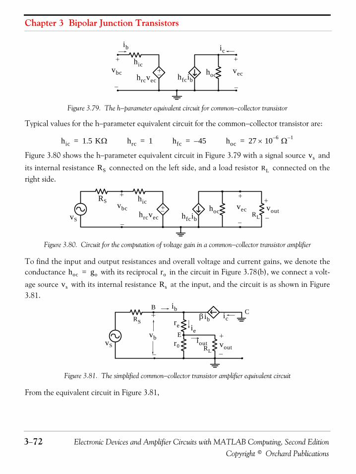
Chapter 3 Bipolar Junction Transistors
3−72 Electronic Devices and Amplifier Circuits with MATLAB Computing, Second EditionCopyright © Orchard Publications
Figure 3.79. The h−parameter equivalent circuit for common−collector transistor
Typical values for the h−parameter equivalent circuit for the common−collector transistor are:
Figure 3.80 shows the h−parameter equivalent circuit in Figure 3.79 with a signal source and
its internal resistance connected on the left side, and a load resistor connected on theright side.
Figure 3.80. Circuit for the computation of voltage gain in a common−collector transistor amplifier
To find the input and output resistances and overall voltage and current gains, we denote theconductance with its reciprocal in the circuit in Figure 3.78(b), we connect a volt-
age source with its internal resistance at the input, and the circuit is as shown in Figure3.81.
Figure 3.81. The simplified common−collector transistor amplifier equivalent circuit
From the equivalent circuit in Figure 3.81,
vechochfcib
hic
hrcvec
vbc
ib ic
hic 1.5 KΩ= hrc 1= hfc 45–= hoc 27 10 6– Ω 1–×=
vs
RS RL
vechochfcib
hic
hrcvec
vbcRL
voutvS
RS
hoc go= ro
vs Rs
ib
voutr0
βib
vb
ic
iere
E
CB
RL
RS
vSiout
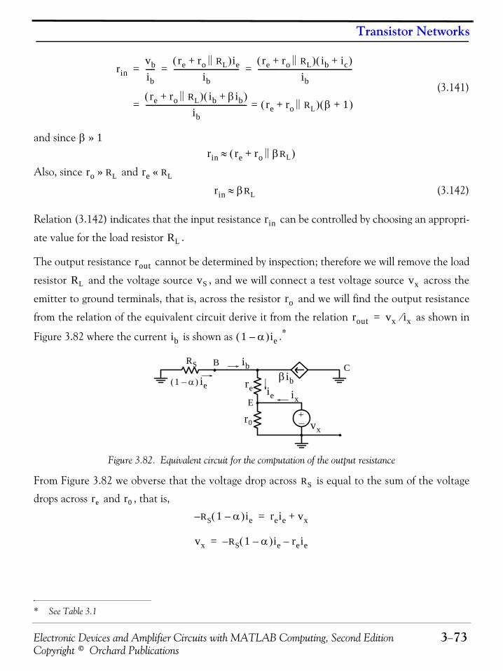
Electronic Devices and Amplifier Circuits with MATLAB Computing, Second Edition 3−73Copyright © Orchard Publications
Transistor Networks
(3.141)
and since
Also, since and
(3.142)
Relation (3.142) indicates that the input resistance can be controlled by choosing an appropri-
ate value for the load resistor .
The output resistance cannot be determined by inspection; therefore we will remove the load
resistor and the voltage source , and we will connect a test voltage source across the
emitter to ground terminals, that is, across the resistor and we will find the output resistance
from the relation of the equivalent circuit derive it from the relation as shown in
Figure 3.82 where the current is shown as .*
Figure 3.82. Equivalent circuit for the computation of the output resistance
From Figure 3.82 we obverse that the voltage drop across is equal to the sum of the voltage
drops across and , that is,
* See Table 3.1
rinvbib-----
re ro RL||+( )ieib
-----------------------------------re ro RL||+( ) ib ic+( )
ib---------------------------------------------------= = =
re ro RL||+( ) ib βib+( )ib
------------------------------------------------------ re ro RL||+( ) β 1+( )==
β 1»
rin re ro βRL||+( )≈
ro RL» re RL«
rin βRL≈
rin
RL
rout
RL vS vx
ro
rout vx ix⁄=
ib 1 α–( )ie
1 α–( ) ie
vxr0
βibie
re
E
CRS
ix
B ib
RS
re r0
R– S 1 α–( )ie reie vx+=
vx R– S 1 α–( )ie reie–=
Chapter 3 Bipolar Junction Transistors
3−74 Electronic Devices and Amplifier Circuits with MATLAB Computing, Second EditionCopyright © Orchard Publications
(3.143)
Also,
or
(3.144)
Substitution of (3.143) into (3.144) yields
and division of both sides by yields
The last relation above reminds us of the formula for the combination of two parallel resistors.Then,
(3.145)
and obviously the output resistance is quite low. The voltage gain is
where from Figure 3.81 and relation (3.141),
(3.146)
vxie-----– RS 1 α–( ) re+=
iev– x
RS 1 α–( ) re+----------------------------------=
r0 ie ix+( ) vx=
ixvxr0----- ie–=
ixvxr0-----
vxRS 1 α–( ) re+----------------------------------+=
vx
ixvx----- 1
rout-------- 1
ro---- 1
RS 1 α–( ) re+----------------------------------+= =
rout ro RS 1 α–( ) re+|| roRS
β 1+------------|| re+= = ro
RS
β-----||
ro RS β⁄⋅ro RS β⁄+-----------------------=≈
AvvoutvS
---------voutvb
---------vbvS-----⋅= =
vbrin
RS rin+------------------vS=
vbvS-----
rinRS rin+------------------
βRL
RS βRL+----------------------≈=
voutro RL||
re ro RL||+--------------------------- vb⋅=

Electronic Devices and Amplifier Circuits with MATLAB Computing, Second Edition 3−75Copyright © Orchard Publications
Transistor Networks
(3.147)
and thus
(3.148)
Relation (3.148) reveals that the voltage gain of the emitter−follower is less than unity. The cur-rent gain is
where by the current division expression
and thus
Since ,
(3.149)
Example 3.19
Figure 3.83 shows the equivalent circuit of a typical emitter−follower and it is given that .Find the input and output resistances and voltage and current gains.
Figure 3.83. Emitter−follower transistor amplifier equivalent circuit for Example 3.19
Solution:
From (3.142)
From (3.145)
voutvb
---------ro RL||
re ro RL||+--------------------------- RL
re RL+-----------------≈=
AvvoutvS
---------voutvb
---------vbvS-----⋅
RL
re RL+-----------------
βRL
RS βRL+----------------------⋅
βRL2
re RL+( ) RS βRL+( )⋅------------------------------------------------------=≈= =
Aiioutib
--------=
ioutro
ro RL+---------------- ie⋅
roro RL+---------------- β 1+( )ib⋅= =
Aiioutib
--------β 1+( )ro
ro RL+----------------------
βroro RL+----------------≈= =
ro RL»
Ai β≈
β 80=
ib
voutr0
βib
vb
icie
re
E
CB
RL
RS
vS
iout
5 KΩ
2 KΩ
10 Ω
30 KΩ
rin βRL 80 2 103×× 160 KΩ= =≈
Chapter 3 Bipolar Junction Transistors
3−76 Electronic Devices and Amplifier Circuits with MATLAB Computing, Second EditionCopyright © Orchard Publications
From (3.148)
This is the voltage gain with a load resistor connected to the circuit. With this resistor discon-nected, the input resistance as given by (3.141) where , is reduced to
(3.150)and (3.146) becomes
(3.151)
Also, (3.147) becomes
(3.152)
Then, the voltage gain with the load resistor disconnected is
(3.153)
and since this relation reduces to
(3.154)
With the given values
and from (3.149)
3.15.6 The T−Equivalent Circuit for the Common−Collector Transistor Amplifier
Figure 3.84 shows the common−collector T−equivalent circuit.
routro RS β⁄⋅ro RS β⁄+----------------------- 30 103× 5 103×× 80⁄
30 103× 5 103× 80⁄+------------------------------------------------------=≈ 62.4 Ω=
AvβRL
2
re RL+( ) RS βRL+( )⋅------------------------------------------------------ 80 4× 106×
10 2 103×+( ) 5 103× 80 2× 10³×+( )--------------------------------------------------------------------------------------------- 0.965= =≈
β 1»
rin β re ro+( )≈
vbvS-----
rinRS rin+------------------
β re ro+( )RS β re ro+( )+------------------------------------≈=
voutvb
---------ro
re ro+---------------=
Av RL ∞→
voutvS
---------voutvb
---------vbvS-----⋅
rore ro+---------------
β re ro+( )RS β re ro+( )+------------------------------------⋅= = =
re ro«
Av RL ∞→
βroRS βro+--------------------=
Av RL ∞→
80 30 103××5 103× 80 30 103××+-------------------------------------------------------- 0.998= =
Ai β 80≈ ≈

Electronic Devices and Amplifier Circuits with MATLAB Computing, Second Edition 3−77Copyright © Orchard Publications
Transistor Cutoff and Saturation Regions
Figure 3.84. T−equivalent model for the common−collector transistor amplifier
As with the T-equivalent models for the common-base and common-emitter transistors, weassume that
and with these assumptions the input and output resistances and voltage and current gains for theT−equivalent model for the common−collector transistor amplifier are:
(3.155)
(3.156)
(3.157)
(3.158)
Table 3.4 summarizes the three possible transistor amplifier configurations.
3.16 Transistor Cutoff and Saturation RegionsAs mentioned earlier, a transistor can be in a cutoff, active, or saturation region. The conditions
TABLE 3.4 Phase, input and output resistances, and voltage and current gains for transistor amplifiers Common−Base Common−Emitter Common Collector
Input/Output Phase
Input Resistance Low Moderate High
Output Resistance Equal to High Low
Voltage Gain Depends on ratio High Close to unity
Current Gain Close to unity High Large
rb
ib
rc
re
βib
ie
vS
RSRL
ic vout
re rc«
rb rc«
RL rc<
Input resis cetan rinRL
1 α–------------= =
Output resis cetan rout re rb RS+( ) 1 α–( )+= =
Voltage gain Av 1≈=
Current gain Ai β≈=
0° 180° 0°rin
rout RC
Av RC RS⁄
Ai
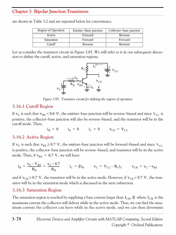
Chapter 3 Bipolar Junction Transistors
3−78 Electronic Devices and Amplifier Circuits with MATLAB Computing, Second EditionCopyright © Orchard Publications
are shown in Table 3.2 and are repeated below for convenience.
Let us consider the transistor circuit in Figure 3.85. We will refer to it in our subsequent discus-sion to define the cutoff, active, and saturation regions.
Figure 3.85. Transistor circuit for defining the regions of operation
3.16.1 Cutoff RegionIf is such that , the emitter−base junction will be reverse−biased and since ispositive, the collector−base junction will also be reverse−biased, and the transistor will be in thecutoff mode. Then,
3.16.2 Active RegionIf is such that , the emitter−base junction will be forward−biased and since is positive, the collector−base junction will be reverse−biased, and transistor will be in the activemode. Then, if , we will have
and if , the transistor will be in the active mode. However, if , the tran-sistor will be in the saturation mode which is discussed in the next subsection.
3.16.3 Saturation RegionThe saturation region is reached by supplying a base current larger than where is themaximum current the collector will deliver while in the active mode. Thus, we can find the max-imum current the collector can have while in the active mode, and we can then determine
Region of Operation Emitter−Base junction Collector−base junctionActive Forward Reverse
Saturation Forward ForwardCutoff Reverse Reverse
VCCRC
vBEvS
iC
+−
+
−vCE
iB
RB iE+−
+
−
vS vBE 0.6 V< VCC
iB 0= iE 0= iC 0= vCE VCC=
vS vBE 0.7 V≥ VCC
vBE 0.7 V=
iBvS VBE–
RB--------------------- vS 0.7–
RB------------------= = iC βiB= vC VCC RCiC–= vCB vC vBE–=
vCB 0.7 V≥ vCB 0.7 V<
ICM β⁄ ICM
Electronic Devices and Amplifier Circuits with MATLAB Computing, Second Edition 3−79Copyright © Orchard Publications
Transistor Cutoff and Saturation Regions
whether the transistor is in the active mode or the saturation mode.
With reference to the circuit in Figure 3.85, the maximum current the collector can havewhile in the active mode can be found from the relation
or
(3.159)
and if is the base current corresponding to the collector current , it follows that
(3.160)
We can also find the maximum value of the applied signal voltage that will keep the transistorin the active mode from the relation
(3.161)
If we increase the base current above , there will be a corresponding increase in and since
, will decrease and if it falls below the value of , the collector−base junc-
tion will become forward−biased and if it reaches a value of , any further increase in thebase current will result in a very small increase in the collector current, and whereas
in the active mode, we can see that this relation does not hold when the transistor
is in the saturation mode. In this case is referred to as the current gain at saturation and it isdenoted as .
When a transistor is deeply into saturation, the collector to emitter voltage is denoted as
and its value is approximately , that is,
(3.162)
and the corresponding collector current is found from the relation
(3.163)
Example 3.20
For the transistor circuit in Figure 3.86 it is known that it is in the active mode and . Find, , , , and .
ICM
RCICM vBE+ VCC=
ICMVCC vBE–
RC------------------------ VCC 0.7–
RC-----------------------= =
IBM ICM
IBM ICM β⁄=
vS
vS max RBIBM 0.7+=
IBM ICM
vC VCC RCIC–= vC vBE
0.6 V
β diC diB⁄=
ββsat
vCE sat
0.2 V
vCE sat 0.2 V≈
iC sat
iC satVCC vCE sat–
RC-------------------------------=
β 50>vE iE vC iC iB
Chapter 3 Bipolar Junction Transistors
3−80 Electronic Devices and Amplifier Circuits with MATLAB Computing, Second EditionCopyright © Orchard Publications
Figure 3.86. Circuit for Example 3.20Solution:
We do not know whether the transistor operates in the cutoff, active, or saturation region, butsince , it is safe to assume that it operates either in the active or saturation region.Assuming active mode of operation, we obtain
and since , let us assume that
Then, in active mode of operation
and since this value is much less that , we conclude that the transistor is deeply intosaturation. Then, in saturation
and
and this is indeed a very large base current. We now can find the value of at saturation.
This value also indicates that the transistor is deeply into saturation.
12 VRC
vBEvS
iC
+
−
vCiB
RB
iE
RE
vB
5 KΩ
3 KΩvE
+
+
+
+ +
−
−
−
−
−
8 V
B
E
C
vB 8 V=
vE vB vBE– 8 0.7– 7.3 V= = =
iEvE
RE------ 7.3
3 103×----------------- 2.43 mA= = =
iC αiE≈iC 2.3 mA≈
vC VCC RCiC– 12 5 103× 2.3 10 3–××– 0.5 V= = =
vB 8 V=
vC vCE sat vE+ 0.2 7.3+ 7.5 V= = =
iCVCC vC–
5 103×---------------------- 12 7.5–
5 103×------------------- 0.90 mA= = =
iB iE iC– 2.43 0.90– 1.53 mA= = =
β
βsatiC
iB---- 0.90
1.53---------- 0.59= = =
Electronic Devices and Amplifier Circuits with MATLAB Computing, Second Edition 3−81Copyright © Orchard Publications
The Ebers−Moll Transistor Model
3.17 The Ebers−Moll Transistor Model
The Ebers−Moll model of the bipolar transistor provides a simple, closed−form expression for thecollector, base, and emitter currents of a bipolar transistor in terms of the terminal voltages. It isvalid in all regions of operation of the bipolar transistor, transitioning between them smoothly.The Ebers−Moll bipolar transistor model expresses each of the terminal currents in terms of a for-ward component , which only depends on the base−to−emitter voltage, and a reverse compo-
nent , which only depends on the base−to−collector voltage.
Let denote the current amplification in the normal operation ( and
) and denote the inverted operation (
and ) common−base current gains of the bipolar transistor, and and
denote the normal and inverted operations respectively of the common−emitter gains. Then,the terminal currents can be expressed as
(3.164)
These current gains are related to one another by
(3.165)
By substituting these relationships into (3.164), we can show that the Ebers−Moll model satisfiesKirchhoff’s current law, that is,
(3.166)
If the emitter−base junction is forward biased and the collector−base junction is reverse biased,then and the bipolar transistor is said to be in the forward−active mode of operation. Inthis case, the terminal currents are given by
(3.167)
Figure 3.87 shows how an NPN and a PNP transistors are biased.
IF
IR
αF VBE forward biased–=
VCB reverse biased–= αR VBE reverse biased–=
VCB forward biased–= βF
βR
IC IFIR
αR------–= IE
IF
αR------ IR–= IE
IF
βF----- I
β---+=
αF R,βF R,
βF R, 1+-------------------= βF R,
αF R,
1 αF R,–-------------------=
IE IC IB+=
IF IR»
IC IF= IEIF
αF------= IB
IF
βF-----=

Chapter 3 Bipolar Junction Transistors
3−82 Electronic Devices and Amplifier Circuits with MATLAB Computing, Second EditionCopyright © Orchard Publications
Figure 3.87. Biased bipolar transistors showing the direction of conventional current flow
To bias an NPN bipolar transistor into the forward−active region, we should ensure that and . In this case, , , and are positive and are flowing in the direc-
tions indicated. To bias a PNP bipolar transistor into the forward−active region, we should ensurethat and . In this case, , , and are positive and are flowing in thedirections indicated.
By using (3.166) and (3.167), we can express the terminal currents in terms of one another as
(3.168)
If the collector−base junction is forward biased, and the emitter−base junction is reverse biased,then and the transistor is said to be in the reverse−active mode of operation in which thecollector and emitters effectively reverse their roles. In this case the terminal currents are givenby
(3.169)
By using (3.166) and (3.169), we can express the terminal currents in terms of one another as
(3.170)
If both junctions are forward biased simultaneously, the transistor is said to be in saturation.
Let be the saturation current and the thermal voltage. Then for the NPN bipolar transis-
tor biased as shown in Figure 3.87, the forward current component, , is given by
(3.171)
Likewise, the reverse current component is
(3.172)
E
C
B
E
CB
NPN Transistor PNP Transistor
IE
IC
IBIBIE
IC
+
−VB
VE
VC
VB
VC
VE−
−
−
−
−
++
+
+
+
VBE 4VT> VC VB≥ IC IE IB
VEB 4VT> VC VB≤ IC IE IB
IC βFIB αFIE= = IEIC
αF------ βF 1+( )IB= = IB
IC
βF----- IE
βF 1+---------------= =
IR IF»
IC IR αR⁄–= IE IR–= IB IR βR⁄=
IE βRIB– αRIC= = IC βR 1+( )IB– IE αR⁄= =
IS VT
IF
IF IS eVBE VT⁄
1–( ) IS eVB VE–( ) VT⁄
1–( )= =
IR
IR IS eVBC VT⁄
1–( ) IS eVB VC–( ) VT⁄
1–( )= =
Electronic Devices and Amplifier Circuits with MATLAB Computing, Second Edition 3−83Copyright © Orchard Publications
The Ebers−Moll Transistor Model
By substitution of (3.171) and (3.172) into (3.164) we express the terminal currents in terms ofthe terminal voltages as
(3.173)
If and , the transistor is biased deeply into the forward−active region and(3.172) reduces to
(3.174)
If and , the transistor is biased deeply into the reverse−active region and(3.173) reduces to
(3.175)
If and , the transistor is deeply saturated and (3.173) can be expressed as
(3.176)
If and , the transistor is deeply into the cutoff region and (3.173) can beexpressed as
(3.177)
For the PNP transistor shown in Figure 3.86, the forward current component, , is given by
(3.178)
IC IS eVB VE–( ) VT⁄
1–( )IS
αR------ e
VB VC–( ) VT⁄1–( )–=
IEIS
αR------ e
VB VE–( ) VT⁄1–( ) IS e
VB VC–( ) VT⁄1–( )–=
IBIS
βF----- e
VB VE–( ) VT⁄1–( )
IS
βR------ e
VB VC–( ) VT⁄1–( )–=
VBE 4VT> VC VB≥
IC IS eVB VE–( ) VT⁄
( )≈ IEIS
αF------ e
VB VE–( ) VT⁄( )≈ IB
IS
βF----- e
VB VE–( ) VT⁄( )≈
VBC 4VT> VE VB>
ICIS
αR------– e
VB VC–( ) VT⁄( )≈ IE IS– e
VB VC–( ) VT⁄( )≈ IB
IS
βR------ e
VB VC–( ) VT⁄( )≈
VBE 4VT> VBC 4VT>
IC IS eVB VE–( ) VT⁄
( )IS
αR------ e
VB VC–( ) VT⁄( )–≈
IEIS
αF------ e
VB VE–( ) VT⁄( ) IS e
VB VC–( ) VT⁄( )–≈
IBIS
βF----- e
VB VE–( ) VT⁄( )
IS
βR------ e
VB VC–( ) VT⁄( )+≈
VBE 4– VT< VBC 4– VT<
ICIS
βR------≈ IE
IS
βF-----≈ IB
IS
βF-----–
IS
βR------–≈
IF
IF IS eVEB VT⁄
1–( ) IS eVE VEB–( ) VT⁄
1–( )= =

Chapter 3 Bipolar Junction Transistors
3−84 Electronic Devices and Amplifier Circuits with MATLAB Computing, Second EditionCopyright © Orchard Publications
and the reverse current component, , is given by
(3.179)
From the Ebers−Moll model equations we can derive relationships for small signal parameters.First, we will find the incremental resistance seen looking into the base terminal of an NPN tran-sistor with the emitter voltage held fixed. From (3.174), that is,
(3.180)
we obtain this incremental base resistance by differentiating with respect to , which yields
or(3.181)
Next, we shall compute the incremental resistance seen looking into the emitter terminal withthe base voltage held constant. From (3.174), that is,
(3.182)
we obtain this incremental emitter resistance by differentiating with respect to , whichyields
or(3.183)
Now, we shall define the incremental transconductance gain of the NPN transistor as the partialderivative of the collector current with respect to the base voltage. From (3.174)
(3.184)
we can obtain this incremental transconductance gain as
IR
IR IS eVCB VT⁄
1–( ) IS eVC VB–( ) VT⁄
1–( )= =
IBIS
βF----- e
VB VE–( ) VT⁄( )≈
IB VB
rb∂VB
∂IB----------
∂IB
∂VB----------⎝ ⎠
⎛ ⎞1– 1
VT-------
IS
βF----- e
VB VE–( ) VT⁄( )
IB
⎝ ⎠⎜ ⎟⎜ ⎟⎛ ⎞ 1–
= = =
⎧ ⎪ ⎪ ⎨ ⎪ ⎪ ⎩
rbVT
IB-------=
IEIS
αF------ e
VB VE–( ) VT⁄( )≈
IE– VE
re∂VE
∂ IE–( )----------------
∂IE
∂VE----------⎝ ⎠
⎛ ⎞1–
– 1VT-------–⎝ ⎠
⎛ ⎞ IS
αF------ e
VB VE–( ) VT⁄( )
IE
⎝ ⎠⎜ ⎟⎛ ⎞
⎝ ⎠⎜ ⎟⎜ ⎟⎛ ⎞
–
1–
= = =
⎧ ⎪ ⎪ ⎨ ⎪ ⎪ ⎩
re VT IE⁄=
IC IS eVB VE–( ) VT⁄
( )≈
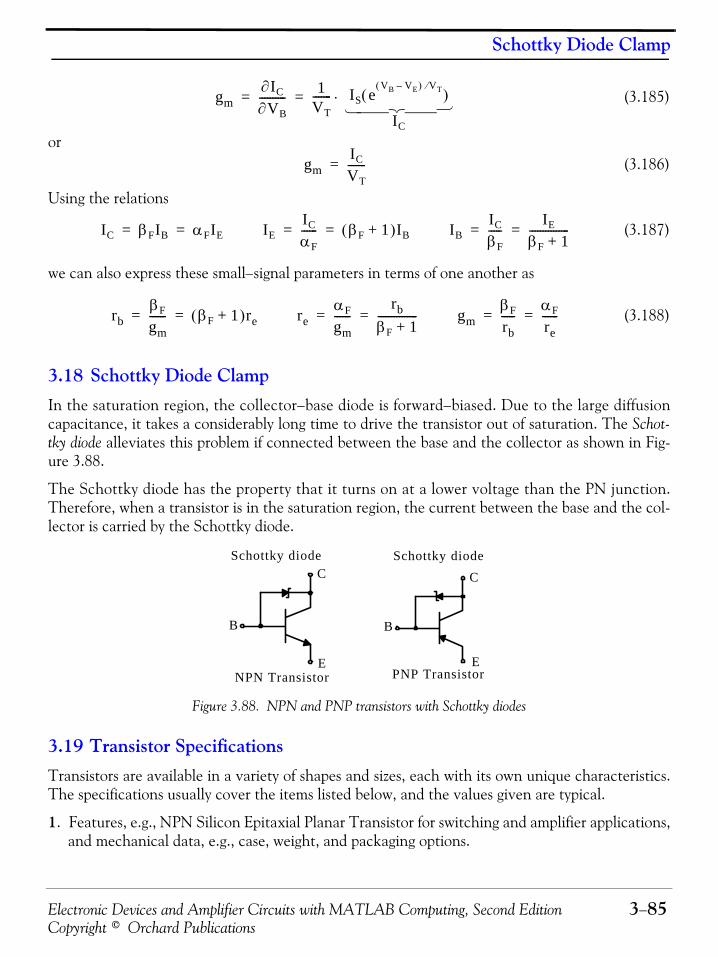
Electronic Devices and Amplifier Circuits with MATLAB Computing, Second Edition 3−85Copyright © Orchard Publications
Schottky Diode Clamp
(3.185)
or(3.186)
Using the relations
(3.187)
we can also express these small−signal parameters in terms of one another as
(3.188)
3.18 Schottky Diode ClampIn the saturation region, the collector−base diode is forward−biased. Due to the large diffusioncapacitance, it takes a considerably long time to drive the transistor out of saturation. The Schot-tky diode alleviates this problem if connected between the base and the collector as shown in Fig-ure 3.88.
The Schottky diode has the property that it turns on at a lower voltage than the PN junction.Therefore, when a transistor is in the saturation region, the current between the base and the col-lector is carried by the Schottky diode.
Figure 3.88. NPN and PNP transistors with Schottky diodes
3.19 Transistor SpecificationsTransistors are available in a variety of shapes and sizes, each with its own unique characteristics.The specifications usually cover the items listed below, and the values given are typical.
1. Features, e.g., NPN Silicon Epitaxial Planar Transistor for switching and amplifier applications,and mechanical data, e.g., case, weight, and packaging options.
gm∂IC
∂VB---------- 1
VT------- IS e
VB VE–( ) VT⁄( )
IC
⋅= =
⎧ ⎪ ⎪ ⎨ ⎪ ⎪ ⎩
gmIC
VT-------=
IC βFIB αFIE= = IEIC
αF------ βF 1+( )IB= = IB
IC
βF----- IE
βF 1+---------------= =
rbβF
gm------ βF 1+( )re= = re
αF
gm------
rbβF 1+---------------= = gm
βF
rb----- αF
re------= =
E
C
B
E
C
B
NPN Transistor PNP Transistor
Schottky diodeSchottky diode

Chapter 3 Bipolar Junction Transistors
3−86 Electronic Devices and Amplifier Circuits with MATLAB Computing, Second EditionCopyright © Orchard Publications
2. Maximum Ratings and Thermal Characteristics, e.g., collector−emitter, collector−base, andemitter base voltages, collector current, power dissipation at room temperature, thermal resis-tance, etc.
3. Electrical Characteristics, e.g., breakdown voltages, saturation voltages, cutoff currents, noisefigure, delay, rise, fall, and storage times, etc. For example, some of the electrical characteris-tics for the 2N3904 NPN are listed as follows:
(DC current gain): min , typical at ,
(Input impedance): min , max at ,
(Voltage feedback ratio): min , max at , ,
(Small signal current gain): min , max at , ,
(Output admittance): min , max at , ,
(Gain−Bandwidth product): at , ,
hFE 100 300 VCE 1 V= IC 10 mA=
hie 1 KΩ 10 KΩ VCE 1 V= IC 10 mA=
hre 0.5 10 4–× 8 10 4–× VCE 10 V= IC 1 mA=
f 100 MHz=
hfe 100 400 VCE 10 V= IC 1 mA=
f 1 KHz=
hoe 1 μΩ 1– 40 μΩ 1– VCE 10 V= IC 1 mA=
f 1 KHz=
fT 300 MHz VCE 20 V= IC 10 mA= f 100 MHz=
Electronic Devices and Amplifier Circuits with MATLAB Computing, Second Edition 3−87Copyright © Orchard Publications
Summary
3.20 Summary• Transistors are three terminal devices that can be formed with the combination of two separate
PN junction materials into one block.
• An NPN transistor is formed with two PN junctions with the P−type material at the center,whereas a PNP transistor is formed with two PN junctions with the N−type material at the cen-ter.
• The three terminals of a transistor, whether it is an NPN or PNP transistor, are identified asthe emitter, the base, and the collector.
• Transistors are used either as amplifiers or as electronic switches.
• Like junction diodes, most transistors are made of silicon. Gallium Arsenide (GaAs) technol-ogy has been under development for several years and its advantage over silicon is its speed,about six times faster than silicon, and lower power consumption. The disadvantages of GaAsover silicon is that arsenic, being a deadly poison, requires very special manufacturing pro-cesses.
• Since a transistor is a 3−terminal device, there are three currents, the base current, denoted as, the collector current, denoted as , and the emitter current, denoted as .
• For any transistor, NPN or PNP, the three currents are related as
• In a transistor the collector current is defined as
where is the reverse (saturation) current, typically to as in junction
diodes, is the base−to−emitter voltage, and at .
• A very useful parameter in transistors is the common−emitter gain , a constant whose valueranges from 75 to 300. Its value is specified by the manufacturer. The base current is much
smaller than the collector current and these two currents are related in terms of the con-
stant as
• Another important parameter in transistors is the common−base current gain denoted as andrelates the collector and emitter currents as
• The parameters and are related as
iB iC iE
iB iC+ iE=
iC IrevBE VT⁄
=
Ir 10 12– A 10 15– AvBE VT 26 mV≈ T 300 °K=
βiB
iC
βiB iC β⁄=
α
iC αiE=
α β
Chapter 3 Bipolar Junction Transistors
3−88 Electronic Devices and Amplifier Circuits with MATLAB Computing, Second EditionCopyright © Orchard Publications
• As with diodes, the base−emitter voltage decreases approximately for each
rise in temperature when the emitter current remains constant.
• In a transistor, the output resistance looking into the collector is defined as
where is the Early voltage supplied by the manufacturer, and is the DC collector cur-rent.
• Two common methods of biasing a transistor are the fixed bias method and the self−biasmethod.
• There are four classes of amplifier operations: Class A, Class AB, Class B, and Class C.
• Class A amplifiers operate entirely in the active region and thus the output if a faithful repro-duction of the input signal with some amplification. In a Class A amplifier the efficiency isvery low. Class A amplifiers are used for audio and frequency amplification.
• Class AB amplifiers are biased so that the collector current is cutoff for a portion of one cycleof the input and so the efficiency is higher than that of a Class A amplifier. Class AB amplifi-ers are normally used as push−pull amplifiers to alleviate the crossover distortion of Class Bamplifiers.
• Class B amplifiers are biased so that the collector current is cutoff during one−half of the inputsignal. Therefore, the efficiency in a Class B amplifier is higher than that of a Class AB ampli-fier. Class B amplifiers are used in amplifiers requiring high power output.
• Class C amplifiers are biased so that the collector current flows for less than one−half cycle ofthe input signal. Class C amplifiers have the highest efficiency and are used for radio frequencyamplification in transmitters.
• The operation of a simple transistor circuit can also be described graphically using versus
and versus curves.
• The average power drawn from the collector supply is
α ββ 1+------------=
β α1 α–------------=
vBE 2 mV 1 °CiE
rout∂vCE
∂iC-----------
vBE cons ttan=
VA
IC-------= =
VA IC
iB
vBE iC vCE
PCC VCCIC=

Electronic Devices and Amplifier Circuits with MATLAB Computing, Second Edition 3−89Copyright © Orchard Publications
Summary
• The average power absorbed by the load is
• The average power absorbed by the transistor is
• The piecewise−linear analysis is a practical method of analyzing transistor amplifiers.
• The incremental model for the transistor provides a better approximation than the piece−wiselinear approximation.
• In the incremental model for the transistor the input resistance is the slope of the input volt-age and current characteristics and it accounts for the voltage drop across the base−emitterjunction. Likewise, the output conductance is the slope of the output current and voltage
characteristics. The voltage amplification factor is related to the input characteristics causedby a change in , and the current amplification factor is related to the output characteris-
tics caused by a change in .
• Transistor hybrid parameters provide us with a means to evaluate voltages, currents, andpower in devices that are connected externally to the transistor. The parameters , , , and
are normally denoted by the (hybrid) parameters as , ,
, and . These designations along with the additional notations
, , , and , provide a symmetrical form for the relations of(3.62)and (3.63) as follows:
• In the incremental model for the transistor the current amplification is defined as
• The transconductance, denoted as , and defined as
An approximate value for the transconductance at room temperature is .
PLOAD RLOADIC2 RLOAD ic RMS( )2+=
PC PCC PL–=
rn
go
μvCE β
iB
rn μ β
go h rn h11 hie= = μ h12 hre= =
β h21 hfe= = go h22 hoe= =
vbe v1= ib i1= vce v2= ic i2=
v1 h11 i1 h12 v2+=
i2 h21 i1 h22 v2+=
Ac
Acic
is---=
gm
gmdiC
dvBE------------
iC IC=
iC
VT-------= =
gm 40IC≈

Chapter 3 Bipolar Junction Transistors
3−90 Electronic Devices and Amplifier Circuits with MATLAB Computing, Second EditionCopyright © Orchard Publications
• The high−frequency models for transistors take into consideration the nonlinear resistance that accounts for the voltage drop across the emitter junction, and the capacitance
that exists across the forward−biased emitter junction. For higher frequencies, the effects ofjunction capacitances must be taken into account. Accordingly, the cutoff frequency,denoted as , is defined as
• If is in milliamps,
• The current gain−bandwidth product, denoted as , is an important figure of merit for atransistor and it can be found from the relations
• The Darlington connection consists of two transistors with a common collector point andexhibits a high input impedance and low output impedance. The combined and are
and
• The common−base, common−emitter, and common collector transistor circuits can also berepresented by their h−equivalent and T−equivalent circuits.
• The Ebers−Moll model of the bipolar transistor provides a simple, closed−form expression forthe collector, base, and emitter currents of a bipolar transistor in terms of the terminal volt-ages. It is valid in all regions of operation of the bipolar transistor, transitioning between themsmoothly.
• The Schottky diode has the property that it turns on at a lower voltage than the PN junction.Therefore, when a transistor is in the saturation region, the current between the base and thecollector is carried by the Schottky diode.
rbe Ce
βωβ
ωβ1
rbeCe------------≡
iC
rbe25βiC
---------=
ωT
ωT βωβgm
Ce------=≈
αT βT
αT α1 α2 α1α2–+=
βT β1 β1β2+≈

Electronic Devices and Amplifier Circuits with MATLAB Computing, Second Edition 3−91Copyright © Orchard Publications
Exercises
3.21 Exercises
1. It is known that in a NPN transistor, when the base−to−emitter voltage , the col-
lector current at temperature . Find the range of changes in at
this temperature for the range .
2. It is known that in a NPN transistor, when the base−to−emitter voltage , the
emitter current , and at temperature . Find , , and
.
3. For the NPN transistor circuit below, it is known that and . The cir-
cuit operates at . Find , , , and .
4. For the PNP transistor circuit below, it is known that , and
. The circuit operates at . Find , , and .
5. Find the output resistance for a bipolar junction transistor whose Early voltage is
and the DC collector current is
a.
b.
c.
vBE 0.7 V=
iC 1.2 mA= T 27 °C= vBE
0.2 iC 5 mA≤ ≤
vBE 0.7 V=
iE 1.2 mA= iB 12 μA= T 27 °C= β α
Ir
VE 0.72– V= β 115=
T 27 °C= IE IB IC VC
EC
B10 VIB
IEIC
VCCVC VEE
10 V
RC 6 KΩ= RE 8 KΩ=
VE
RB 130 KΩ= VE 2 V=
VEB 0.7 V= T 27 °C= α β VC
EC
B12 V
IB
IEIC
VCCVC VEE
12 VVE
RC 5 KΩ= RE 10 KΩ=
RB
VB
rout
VA 75 V=
IC 0.1 mA=
IC 1 mA=
IC 5 mA=
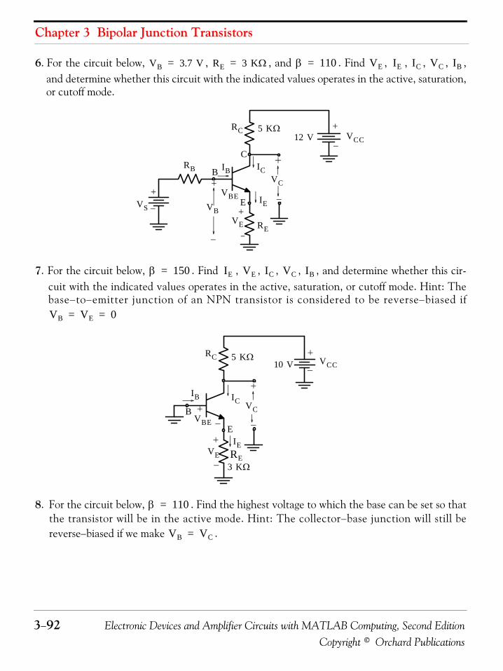
Chapter 3 Bipolar Junction Transistors
3−92 Electronic Devices and Amplifier Circuits with MATLAB Computing, Second EditionCopyright © Orchard Publications
6. For the circuit below, , , and . Find , , , , ,and determine whether this circuit with the indicated values operates in the active, saturation,or cutoff mode.
7. For the circuit below, . Find , , , , , and determine whether this cir-cuit with the indicated values operates in the active, saturation, or cutoff mode. Hint: Thebase−to−emitter junction of an NPN transistor is considered to be reverse−biased if
8. For the circuit below, . Find the highest voltage to which the base can be set so thatthe transistor will be in the active mode. Hint: The collector−base junction will still bereverse−biased if we make .
VB 3.7 V= RE 3 KΩ= β 110= VE IE IC VC IB
E
C
B IB ICRB
VBEVS
VCC
VC
VB
RE
IE
VE
5 KΩRC12 V
β 150= IE VE IC VC IB
VB VE 0= =
E
B
IB IC
VBE
VCC
VC
RE3 KΩ
IEVE
5 KΩRC10 V
β 110=
VB VC=

Electronic Devices and Amplifier Circuits with MATLAB Computing, Second Edition 3−93Copyright © Orchard Publications
Exercises
9. For an NPN transistor circuit , , and with the reverse−
biased collector−base junction set at we want the collector current to be
. What should the values of and be to achieve this value?
10. For a PNP transistor circuit with , , , , and
, what would the largest value of be so that the transistor operates at theactive mode?
11. For a PNP transistor circuit with , , , ,
, and , what should the values of and be so that the tran-sistor operates at the active mode?
12. For the circuit below, it is known that for both transistors. Find all indicated volt-ages and currents. Are both the transistors operating in the active mode? What is the totalpower absorbed by this circuit?
E
C
B IB IC
RB VBEVS
VCC
VC
VBRE
3 KΩ
IEVE
5 KΩRC12 V
β 100= VCC 11.3 V= VB 3.5 V=
VCB 1.8 V=
IC 0.8 mA= RC RE
β 120= VEE 12 V= VB 0 V= VCC 12 V–=
RE 3 KΩ= RC
β 150= VEE 12 V= VB 0 V= VCC 12 V–=
IE 0.8 mA= VCB 3– V= RC RE
β 120=
E1
C1
B1
IB1
IC1
R2
VBE1
VCC
VC1
VB1
RE15 KΩ
IE1VE1
8 KΩRC1
R1 60 KΩ
KΩ
C2
E2
B2IB2 IE2
VEB2VE2
RC28 KΩ
IC2VC2
5 KΩRE2 12 V
10 μAVB2
30
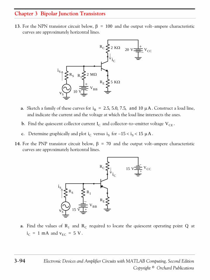
Chapter 3 Bipolar Junction Transistors
3−94 Electronic Devices and Amplifier Circuits with MATLAB Computing, Second EditionCopyright © Orchard Publications
13. For the NPN transistor circuit below, and the output volt−ampere characteristiccurves are approximately horizontal lines.
a. Sketch a family of these curves for . Construct a load line,and indicate the current and the voltage at which the load line intersects the axes.
b. Find the quiescent collector current and collector−to−emitter voltage .
c. Determine graphically and plot versus for .
14. For the PNP transistor circuit below, and the output volt−ampere characteristiccurves are approximately horizontal lines.
a. Find the values of and required to locate the quiescent operating point at
and .
β 100=
iS
+−
−+2 KΩ
vS
RS
iC
2 MΩ
20 V
10 V
R1
RC
VBB
RE 5 KΩ
VCC
iB 2.5 5.0 7.5 and 10 μA, , ,=
IC VCE
iC iS 15 iS 15 μA< <–
β 70=
iS
+
−
−
+
vS
RS
iC
15 V
15 V
R1
RC VCC
VBB
RE
R1 RC QiC 1 mA= vEC 5 V=
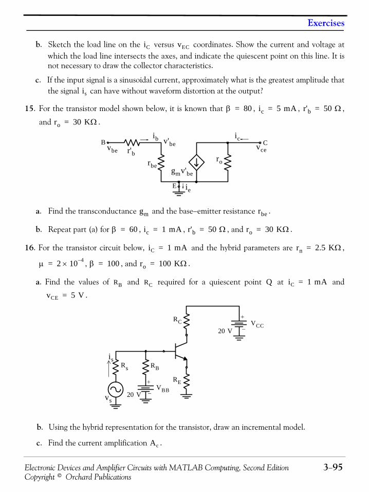
Electronic Devices and Amplifier Circuits with MATLAB Computing, Second Edition 3−95Copyright © Orchard Publications
Exercises
b. Sketch the load line on the versus coordinates. Show the current and voltage atwhich the load line intersects the axes, and indicate the quiescent point on this line. It isnot necessary to draw the collector characteristics.
c. If the input signal is a sinusoidal current, approximately what is the greatest amplitude thatthe signal can have without waveform distortion at the output?
15. For the transistor model shown below, it is known that , , ,
and .
a. Find the transconductance and the base−emitter resistance .
b. Repeat part (a) for , , , and .
16. For the transistor circuit below, and the hybrid parameters are ,
, , and .
a. Find the values of and required for a quiescent point at and
.
b. Using the hybrid representation for the transistor, draw an incremental model.
c. Find the current amplification .
iC vEC
is
β 80= ic 5 mA= r'b 50 Ω=
ro 30 KΩ=
rbe
Bib
vbero
gmv'be
E
icvce
C
ie
r'bv'be
gm rbe
β 60= ic 1 mA= r'b 50 Ω= ro 30 KΩ=
iC 1 mA= rn 2.5 KΩ=
μ 2 10 4–×= β 100= ro 100 KΩ=
RB RC Q iC 1 mA=
vCE 5 V=
is
+
−
−
+
vs
Rs
20 V
20 V
RB
RC VCC
VBB
RE
Ac

Chapter 3 Bipolar Junction Transistors
3−96 Electronic Devices and Amplifier Circuits with MATLAB Computing, Second EditionCopyright © Orchard Publications
17. Determine whether the PNP transistor shown below is operating in the cutoff, active, or sat-uration region
18. The equations describing the parameters can be used to represent the network shownbelow. This network is a transistor equivalent circuit for the common−emitter configurationand the parameters given are typical values for such a circuit. Compute the voltage andcurrent gains for this network if a voltage source of in series with is
connected at the input (left side), and a load is connected at the output (right side).
E
CB
10 V+
−
RC
10 KΩ
2 KΩRE
RB
5 KΩ
VB
10 V +
−VCC
VEE
h
hv1 ωtcos mV= 800 Ω
5 KΩ
− −
+ +h11
+−h12v2 h21i1
v2v1
i1 i2
h22
h11 1.2 KΩ=
h12 2 10 4–×=
h21 50=
h22 50 10 6– Ω 1–×=

Electronic Devices and Amplifier Circuits with MATLAB Computing, Second Edition 3−97Copyright © Orchard Publications
Solutions to End−of−Chapter Exercises
3.22 Solutions to End−of−Chapter Exercises1. From (3.2)
(1)
and as we know from Chapter 2 at , . From the given data
(2)Division of (1) by (2) yields
(3)
With , from (3),
and with ,
Therefore, for , the range is
2. From (3.1)
iC IrevBE VT⁄
=
T 27 °C= VT 26 mV=
1.2 10 3–× Ire0.7 VT⁄
=
iC
1.2 10 3–×------------------------ e
vBE VT⁄
e0.7 VT⁄
----------------=
iC 1.2 10 3–× evBE 0.7–( ) VT⁄
=
iC( )ln 1.2 10 3–× evBE 0.7–( ) VT⁄
( )ln 1.2 10 3–×( )ln vBE 0.7–( ) VT⁄+= =
iC( )ln 1.2 10 3–×( )ln– vBE 0.7–( ) VT⁄=
iC
1.2 10 3–×------------------------⎝ ⎠⎛ ⎞ln vBE 0.7–( ) VT⁄=
VTiC
1.2 10 3–×------------------------⎝ ⎠⎛ ⎞ln vBE 0.7–=
BE 0.7 VTiC
1.2 10 3–×------------------------⎝ ⎠⎛ ⎞ln+ 0.7 26 10 3–×
iC
1.2 10 3–×------------------------⎝⎛ln+= =
iC 0.2 mA=
vBE 0.7 26 10 3–× 0.2 10 3–×1.2 10 3–×------------------------⎝ ⎠⎛ ⎞ln+ 0.7 26 10 3–× 1.792–( )×+ 0.653 V= = =
iC 5 mA=
vBE 0.7 26 10 3–× 5 10 3–×1.2 10 3–×------------------------⎝ ⎠⎛ ⎞ln+ 0.7 26 10 3–× 1.427×+ 0.737 V= = =
0.2 iC 5 mA≤ ≤ vBE 0.653 vBE 0.737 V≤ ≤
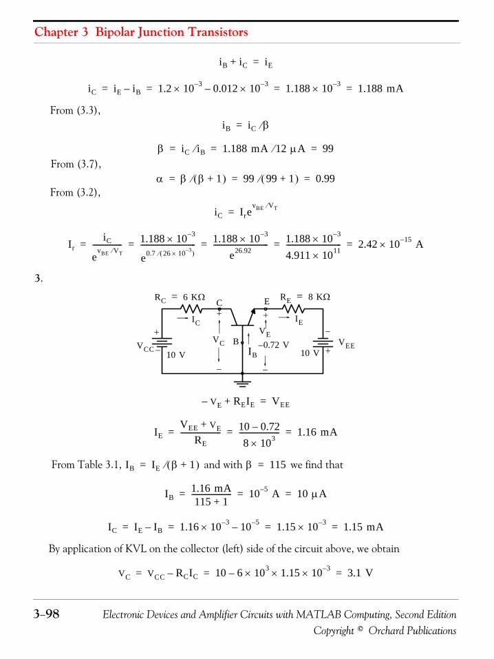
Chapter 3 Bipolar Junction Transistors
3−98 Electronic Devices and Amplifier Circuits with MATLAB Computing, Second EditionCopyright © Orchard Publications
From (3.3),
From (3.7),
From (3.2),
3.
From Table 3.1, and with we find that
By application of KVL on the collector (left) side of the circuit above, we obtain
iB iC+ iE=
iC iE iB– 1.2 10 3–× 0.012 10 3–×– 1.188 10 3–× 1.188 mA= = = =
iB iC β⁄=
β iC iB⁄ 1.188 mA 12 μA⁄ 99= = =
α β β 1+( )⁄ 99 99 1+( )⁄ 0.99= = =
iC IrevBE VT⁄
=
IriC
evBE VT⁄
---------------- 1.188 10 3–×
e0.7 26 10 3–×( )⁄------------------------------ 1.188 10 3–×
e26.92------------------------------ 1.188 10 3–×
4.911 1011×------------------------------ 2.42 10 15–× A= = = = =
EC
B10 VIB
IEIC
VCCVC VEE
10 V
RC 6 KΩ= RE 8 KΩ=
VE0.72– V
VE– REIE+ VEE=
IEVEE VE+
RE---------------------- 10 0.72–
8 103×---------------------- 1.16 mA= = =
IB IE β 1+( )⁄= β 115=
IB1.16 mA115 1+
---------------------- 10 5– A 10 μA= = =
IC IE IB– 1.16 10 3–× 10 5–– 1.15 10 3–× 1.15 mA= = = =
VC VCC RCIC– 10 6 103× 1.15 10 3–××– 3.1 V= = =
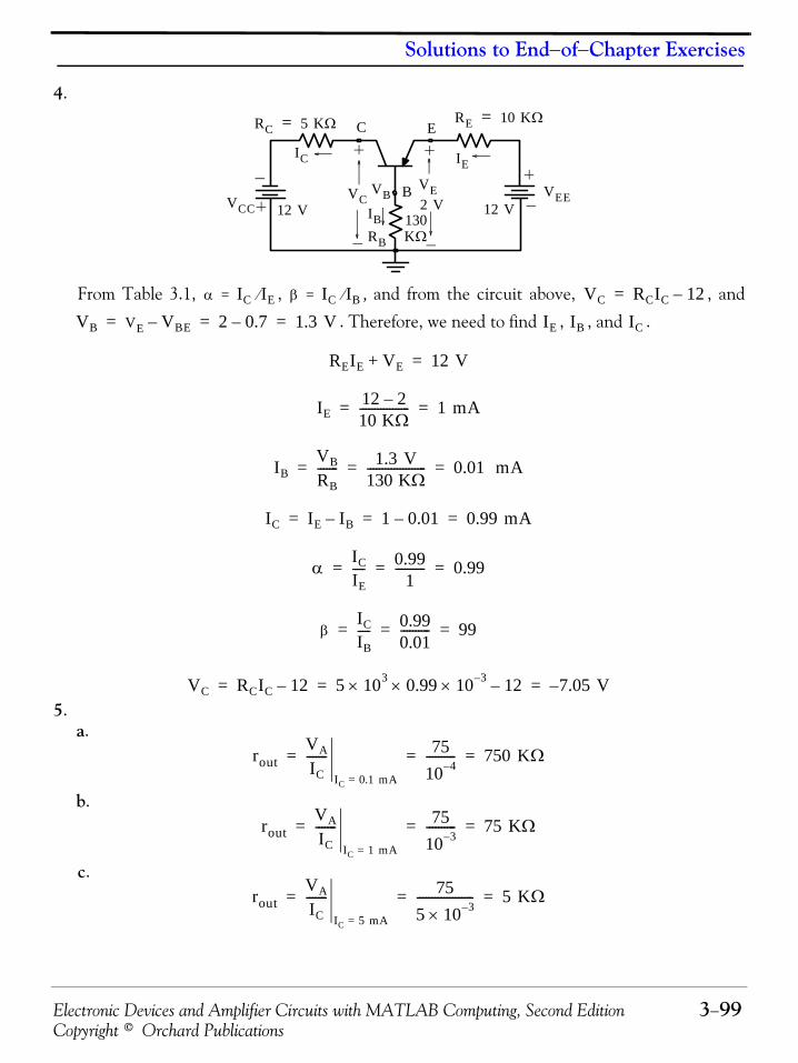
Electronic Devices and Amplifier Circuits with MATLAB Computing, Second Edition 3−99Copyright © Orchard Publications
Solutions to End−of−Chapter Exercises
4.
From Table 3.1, , , and from the circuit above, , and
. Therefore, we need to find , , and .
5.a.
b.
c.
EC
B12 VIB
IEIC
VCCVC VEE
12 V
VE
RC 5 KΩ= RE 10 KΩ=
RB
VB2 V
130KΩ
α IC IE⁄= β IC IB⁄= VC RCIC 12–=
VB VE VBE– 2 0.7– 1.3 V= = = IE IB IC
REIE VE+ 12 V=
IE12 2–10 KΩ----------------- 1 mA= =
IBVB
RB------- 1.3 V
130 KΩ-------------------- 0.01 mA= = =
IC IE IB– 1 0.01– 0.99 mA= = =
αIC
IE----- 0.99
1---------- 0.99= = =
βIC
IB----- 0.99
0.01---------- 99= = =
VC RCIC 12– 5 103× 0.99 10 3–×× 12– 7.05 V–= = =
routVA
IC-------
IC 0.1 mA=
7510 4–---------- 750 KΩ= = =
routVA
IC-------
IC 1 mA=
7510 3–---------- 75 KΩ= = =
routVA
IC-------
IC 5 mA=
755 10× 3–------------------- 5 KΩ= = =

Chapter 3 Bipolar Junction Transistors
3−100 Electronic Devices and Amplifier Circuits with MATLAB Computing, Second EditionCopyright © Orchard Publications
6.
Since it is reasonable to assume that the base−emitter junction is forward−
biased and thus . Then,
and
It is given that . Then,
and
The collector voltage is
This is an NPN transistor and the collector (N) to base (P) must be reverse−biased for thetransistor to operate in the active mode. Since , the transistor is indeed operating inthe active mode and our assumption that the base−emitter junction is forward−biased, is cor-rect.
Finally,
E
C
B IB ICRB
VBEVS
VCC
VC
VB
RE
IE
VE
5 KΩRC12 V
3.7 V
3 KΩ
VB 3.7 V=
VBE 0.7 V=
VE VB VBE– 3.7 0.7– 3 V= = =
IEVE
RE------- 3
3 10 3–×------------------- 1 mA= = =
β 110=
α ββ 1+------------ 110
111--------- 0.991= = =
IC αIE 0.991 1× 0.991 mA= = =
VC VCC RCIC– 12 5 103× 0.991 10 3–××– 7.05V= = =
VC VB>
IB IE IC– 1 0.991– 9 μA= = =
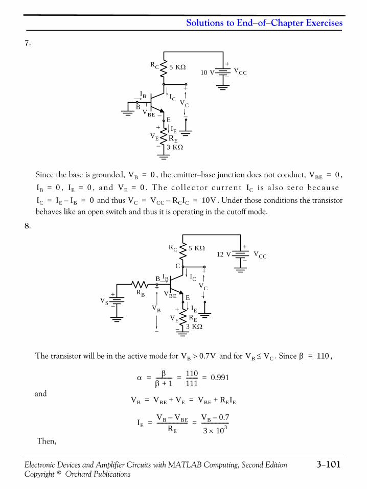
Electronic Devices and Amplifier Circuits with MATLAB Computing, Second Edition 3−101Copyright © Orchard Publications
Solutions to End−of−Chapter Exercises
7.
Since the base is grounded, , the emitter−base junction does not conduct, ,
, , and . The co l l ec to r cu r rent i s a l so z e ro because
and thus . Under those conditions the transistorbehaves like an open switch and thus it is operating in the cutoff mode.
8.
The transistor will be in the active mode for and for . Since ,
and
Then,
E
B
IB IC
VBE
VCC
VC
RE3 KΩ
IEVE
5 KΩRC10 V
VB 0= VBE 0=
IB 0= IE 0= VE 0= IC
IC IE IB– 0= = VC VCC RCIC– 10V= =
E
C
B IB IC
RB VBEVS
VCC
VC
VBRE
3 KΩ
IEVE
5 KΩRC12 V
VB 0.7V> VB VC≤ β 110=
α ββ 1+------------ 110
111--------- 0.991= = =
VB VBE VE+ VBE REIE+= =
IEVB VBE–
RE----------------------- VB 0.7–
3 103×--------------------= =
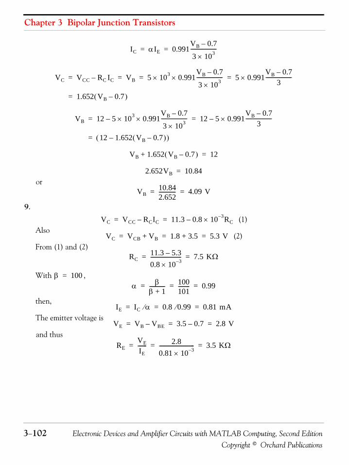
Chapter 3 Bipolar Junction Transistors
3−102 Electronic Devices and Amplifier Circuits with MATLAB Computing, Second EditionCopyright © Orchard Publications
or
9.
(1)Also
(2)From (1) and (2)
With ,
then,
The emitter voltage is
and thus
IC αIE 0.991VB 0.7–
3 103×--------------------= =
VC VCC RC IC– VB 5 103× 0.991VB 0.7–
3 103×--------------------× 5 0.991×
VB 0.7–3
--------------------= = = =
1.652 VB 0.7–( )=
VB 12 5 103× 0.991VB 0.7–
3 103×--------------------×– 12 5 0.991×
VB 0.7–3
--------------------–= =
12 1.652 VB 0.7–( )–( )=
VB 1.652 VB 0.7–( )+ 12=
2.652VB 10.84=
VB10.842.652------------- 4.09 V= =
VC VCC RCIC– 11.3 0.8 10 3–× RC–= =
VC VCB VB+ 1.8 3.5+ 5.3 V= = =
RC11.3 5.3–
0.8 10 3–×------------------------ 7.5 KΩ= =
β 100=α β
β 1+------------ 100
101--------- 0.99= = =
IE IC α⁄ 0.8 0.99⁄ 0.81 mA= = =
VE VB VBE– 3.5 0.7– 2.8 V= = =
REVE
IE------- 2.8
0.81 10 3–×--------------------------- 3.5 KΩ= = =

Electronic Devices and Amplifier Circuits with MATLAB Computing, Second Edition 3−103Copyright © Orchard Publications
Solutions to End−of−Chapter Exercises
10.
A PNP transistor will still be in the active mode if . For this exercise the base is
grounded so and we can let also. Then,
or (1)
where (2)
and from
we obtain (3)
By substitution of (2) and (3) into (1) we obtain
C
E
BIB IE
VEB
VEE
VE
RC3 KΩ
IC
VC
5 KΩRE 12 V
VCC12 V
VC VB=
VB 0= VC 0≈
VC RCIC VCC– RCαIE 12– 0≈= =
RC12αIE--------=
α ββ 1+------------ 120
121--------- 0.992= = =
VE VEB 0.7 VEE REIE– 12 REIE–= = = =
IE12 0.7–
3 103×------------------- 3.77 mA= =
RC12αIE-------- 12
0.992 3.77 10 3–××----------------------------------------------- 3.21 KΩ= = =

Chapter 3 Bipolar Junction Transistors
3−104 Electronic Devices and Amplifier Circuits with MATLAB Computing, Second EditionCopyright © Orchard Publications
11.
Since the base is grounded,
and
Then,
Also, since
then,
or
C
E
BIB
IE
VEB
VEE
VE
RC IC
VC
RE 12 V
VCC12 V
VC VCB 3 V–= =
VE VEB 0.7 V= =
REIE VE+ VEE 12 V= =
RE12 0.7–
0.8 10 3–×------------------------ 14 KΩ= =
IC αIEβ
β 1+------------IE 0.993 0.8× 0.795 mA= = = =
VC RCIC+ V– CC=
RC12–( )– 3–
0.795 10 3–×------------------------------ 11.3 KΩ= =

Electronic Devices and Amplifier Circuits with MATLAB Computing, Second Edition 3−105Copyright © Orchard Publications
Solutions to End−of−Chapter Exercises
12.
The left part in the circuit above is the same as that in Example 3.8 where we applied Theve-nin’s theorem. Therefore the given circuit is redrawn as shown below.
Application of KVL around the left part of the circuit yields
From Table 3.1, . Then,
E1
C1
B1
IB1
IC1
R2
VBE1
VCC
VC1
VB1
RE15 KΩ
IE1VE1
8 KΩRC1
R1 60 KΩ
KΩ
C2
E2
B2IB2 IE2
VEB2VE2
RC28 KΩ
IC2VC2
5 KΩRE2 12 V
10 μAVB2
30
E1
C1
B1IB1
IC1
VBE1
VCC
VC1
VB1
RE15 KΩ
IE1
VE1
8 KΩRC1
C2
E2
B2
IB2 IE2
VEB2VE2
RC28 KΩ
IC2VC2
5 KΩRE212 V
20 KΩ
RTH
VTH4 V
I'C1
10 μA
VB2
RTHIB1 VBE1 RE1IE1+ + VTH=
20 103×( )IB1 0.7 5 103×( )IE1+ + 4=
4IB1 IE1+ 3.35 103×----------------- 0.66 10 3–×= =
IE β 1+( )IB=
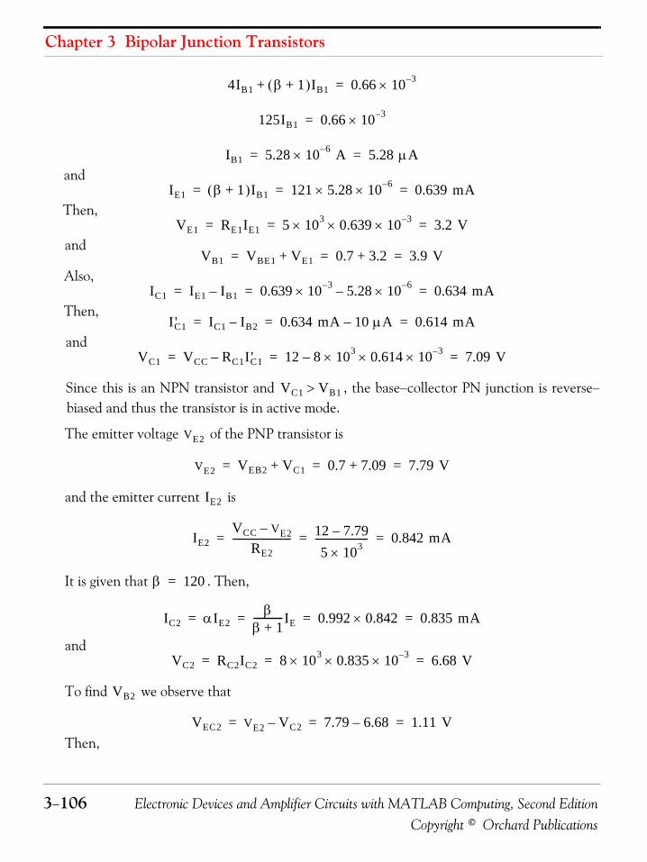
Chapter 3 Bipolar Junction Transistors
3−106 Electronic Devices and Amplifier Circuits with MATLAB Computing, Second EditionCopyright © Orchard Publications
and
Then,
and
Also,
Then,
and
Since this is an NPN transistor and , the base−collector PN junction is reverse−biased and thus the transistor is in active mode.
The emitter voltage of the PNP transistor is
and the emitter current is
It is given that . Then,
and
To find we observe that
Then,
4IB1 β 1+( )IB1+ 0.66 10 3–×=
125IB1 0.66 10 3–×=
IB1 5.28 10 6–× A 5.28 μA= =
IE1 β 1+( )IB1 121 5.28 10 6–×× 0.639 mA= = =
VE1 RE1IE1 5 103× 0.639 10 3–×× 3.2 V= = =
VB1 VBE1 VE1+ 0.7 3.2+ 3.9 V= = =
IC1 IE1 IB1– 0.639 10 3–× 5.28 10 6–×– 0.634 mA= = =
I 'C1 IC1 IB2– 0.634 mA 10 μA– 0.614 mA= = =
VC1 VCC RC1I'C1– 12 8 103× 0.614 10 3–××– 7.09 V= = =
VC1 VB1>
VE2
VE2 VEB2 VC1+ 0.7 7.09+ 7.79 V= = =
IE2
IE2VCC VE2–
RE2------------------------ 12 7.79–
5 103×---------------------- 0.842 mA= = =
β 120=
IC2 αIE2β
β 1+------------IE 0.992 0.842× 0.835 mA= = = =
VC2 RC2IC2 8 103× 0.835 10 3–×× 6.68 V= = =
VB2
VEC2 VE2 VC2– 7.79 6.68– 1.11 V= = =
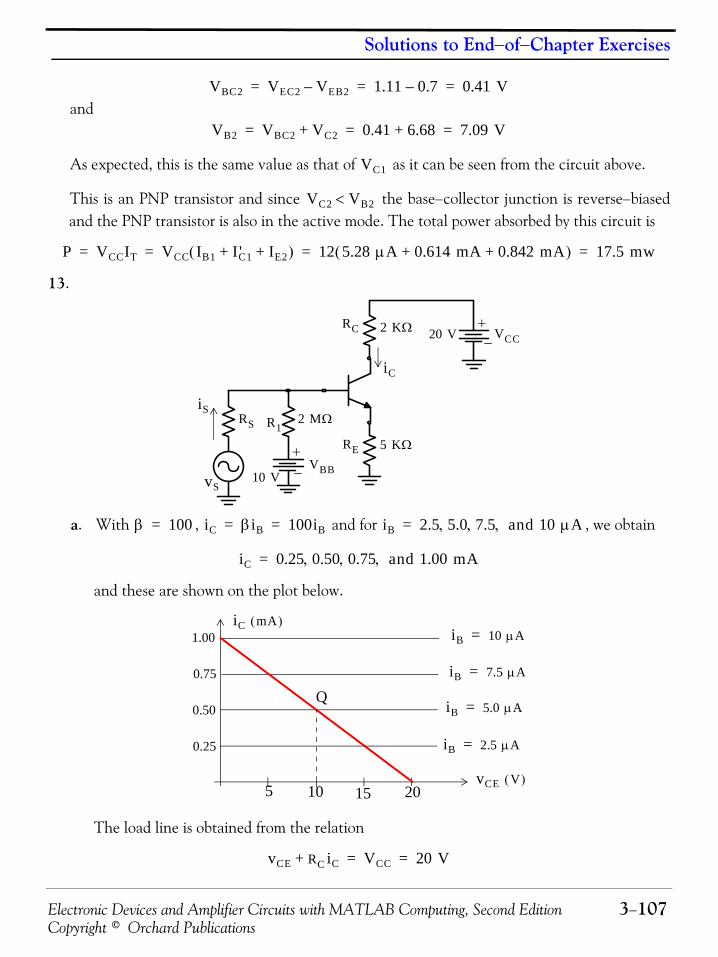
Electronic Devices and Amplifier Circuits with MATLAB Computing, Second Edition 3−107Copyright © Orchard Publications
Solutions to End−of−Chapter Exercises
and
As expected, this is the same value as that of as it can be seen from the circuit above.
This is an PNP transistor and since the base−collector junction is reverse−biasedand the PNP transistor is also in the active mode. The total power absorbed by this circuit is
13.
a. With , and for , we obtain
and these are shown on the plot below.
The load line is obtained from the relation
VBC2 VEC2 VEB2– 1.11 0.7– 0.41 V= = =
VB2 VBC2 VC2+ 0.41 6.68+ 7.09 V= = =
VC1
VC2 VB2<
P VCCIT VCC IB1 I 'C1 IE2+ +( ) 12 5.28 μA 0.614 mA 0.842 mA+ +( ) 17.5 mw= = = =
iS
+−
−+2 KΩ
vS
RS
iC
2 MΩ
20 V
10 V
R1
RC
VBB
RE 5 KΩ
VCC
β 100= iC βiB 100iB= = iB 2.5 5.0 7.5 and 10 μA, , ,=
iC 0.25 0.50 0.75 and 1.00 mA, , ,=
0.25
0.50
0.75
1.00
5 10 15 20
iB 2.5 μA=
iB 5.0 μA=
iB 10 μA=
iB 7.5 μA=
iC mA( )
vCE V( )
Q
vCE RC iC+ VCC 20 V= =

Chapter 3 Bipolar Junction Transistors
3−108 Electronic Devices and Amplifier Circuits with MATLAB Computing, Second EditionCopyright © Orchard Publications
When , , and when , .
The load line then intercepts the axis at and the axis at .
b. As shown above, the point is the intersection of the load line and the line .
Thus with reference to the circuit above and , , and
the point is as shown above and we observe that and .
c.
and
Then, for the range , we obtain the corresponding collector current val-ues as shown on the table below.
The plot below shows the current transfer characteristics
−15 −10 −5 0 5 10 15
0 0 0 5 10 10 10
iC 0= vCE 20 V= vCE 0= iC VCC RC⁄ 20 20 KΩ⁄ 1 mA= = =
vCE 20 V iC 1 mA
Q iB IB=
is 0= IB 10 V 2 MΩ⁄ 5 μA= =
Q IC 0.5 mA= VCE 10 V=
iB IB is+VBB
R1---------- is+ 5 is+= = =
iC βiB β 5 is+( )= =
15 is 15 μA< <–
is μA( )
iC mA( )
iC mA( )
is μA( )10–15– 5– 5 10 15
10
5
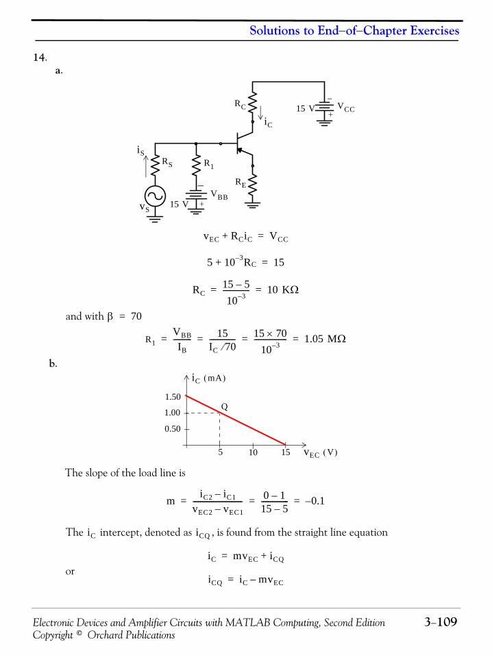
Electronic Devices and Amplifier Circuits with MATLAB Computing, Second Edition 3−109Copyright © Orchard Publications
Solutions to End−of−Chapter Exercises
14.a.
and with
b.
The slope of the load line is
The intercept, denoted as , is found from the straight line equation
or
iS
+
−
−
+
vS
RS
iC
15 V
15 V
R1
RC VCC
VBB
RE
vEC RCiC+ VCC=
5 10 3– RC+ 15=
RC15 5–
10 3–--------------- 10 KΩ= =
β 70=
R1VBB
IB---------- 15
IC 70⁄-------------- 15 70×
10 3–------------------ 1.05 MΩ= = = =
1.50
0.50
1.00
5 10 15
iC mA( )
vEC V( )
Q
m iC2 iC1–vEC2 vEC1–--------------------------- 0 1–
15 5–--------------- 0.1–= = =
iC iCQ
iC mvEC iCQ+=
iCQ iC mvEC–=
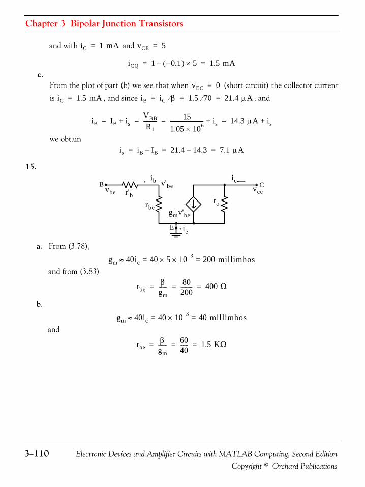
Chapter 3 Bipolar Junction Transistors
3−110 Electronic Devices and Amplifier Circuits with MATLAB Computing, Second EditionCopyright © Orchard Publications
and with and
c.From the plot of part (b) we see that when (short circuit) the collector current
is , and since , and
we obtain
15.
a. From (3.78),
and from (3.83)
b.
and
iC 1 mA= vCE 5=
iCQ 1 0.1–( ) 5×– 1.5 mA= =
vEC 0=
iC 1.5 mA= iB iC β⁄ 1.5 70⁄ 21.4 μA= = =
iB IB is+VBB
R1---------- 15
1.05 106×------------------------- is+ 14.3 μA is+= = = =
is iB IB– 21.4 14.3– 7.1 μA= = =
rbe
Bib
vbero
gmv'be
E
icvce
C
ie
r'bv'be
gm 40ic 40 5 10 3–×× 200 millimhos= =≈
rbeβ
gm------ 80
200--------- 400 Ω= = =
gm 40ic 40 10 3–× 40 millimhos= =≈
rbeβ
gm------ 60
40------ 1.5 KΩ= = =

Electronic Devices and Amplifier Circuits with MATLAB Computing, Second Edition 3−111Copyright © Orchard Publications
Solutions to End−of−Chapter Exercises
16.
a.
b. The incremental model circuit in Figure 3.63 is applicable here and it is shown below withthe given parameters and the values obtained in part (a).
c. From (3.67)
or
is
+
−
−
+
vs
Rs
20 V
20 V
RB
RC VCC
VBB
RE
RCiC vCE+ VCC=
RCVCC vCE–
iC------------------------ 20 5–
10 3–--------------- 15 KΩ= = =
IB IC β⁄ 10 3– 100⁄ 10 μA= = =
RBVBB
IB---------- 20
10 5–---------- 2 MΩ= = =
μβReq–
rnB iB
is
roβib
E
C
RB
Req
Rs2 MΩ
2.5 KΩ
26 Ω–
100iB
iC
KΩ15RC
100KΩ
vCE
Acicis---
RB
RB rn+( )----------------------β
roro RC+( )
----------------------= =
Ac2 106×
2.0025 106×------------------------------- 100 105
1.15 105×-------------------------×× 87≈=
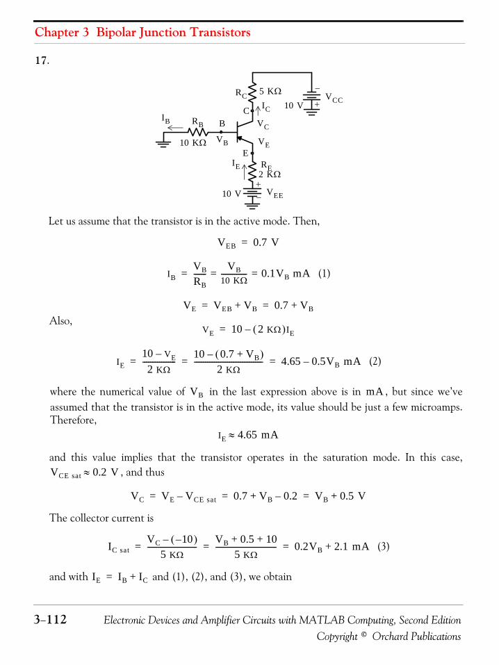
Chapter 3 Bipolar Junction Transistors
3−112 Electronic Devices and Amplifier Circuits with MATLAB Computing, Second EditionCopyright © Orchard Publications
17.
Let us assume that the transistor is in the active mode. Then,
(1)
Also,
(2)
where the numerical value of in the last expression above is in , but since we’veassumed that the transistor is in the active mode, its value should be just a few microamps.Therefore,
and this value implies that the transistor operates in the saturation mode. In this case,, and thus
The collector current is
(3)
and with and (1), (2), and (3), we obtain
E
CB
10 V+
−
RC
10 KΩ
2 KΩ
RB
5 KΩ
VB
10 V +
−VCC
VEE
IB
VE
REIE
VC
IC
VEB 0.7 V=
IBVB
RB------- VB
10 KΩ-------------- 0.1VB mA= ==
VE VEB VB+ 0.7 VB+= =
VE 10 2 KΩ( )IE–=
IE10 VE–
2 KΩ------------------ 10 0.7 VB+( )–
2 KΩ------------------------------------- 4.65 0.5VB mA–= = =
VB mA
IE 4.65 mA≈
VCE sat 0.2 V≈
VC VE VCE sat– 0.7 VB 0.2–+ VB 0.5 V+= = =
IC satVC 10–( )–
5 KΩ--------------------------- VB 0.5 10+ +
5 KΩ--------------------------------- 0.2VB 2.1 mA+= = =
IE IB IC+=

Electronic Devices and Amplifier Circuits with MATLAB Computing, Second Edition 3−113Copyright © Orchard Publications
Solutions to End−of−Chapter Exercises
Solving for ,
Then
Also,
18. We recall that (1)
(2)
With the voltage source in series with connected at the input and a load connected at the output the network is as shown below.
The network above is described by the equations
or
We write the two equations above in matrix form and use MATLAB for the solution.
A=[2*10^3 2*10^(−4); 50 250*10^(−6)]; B=[10^(−3) 0]'; X=A\B;...fprintf(' \n'); fprintf('i1 = %5.2e A \t',X(1)); fprintf('v2 = %5.2e V',X(2))
4.65 VB– 0.1VB 0.2VB 2.1+ +=
VB
VB2.551.3---------- 1.96 V= =
IB1.96
10 KΩ-------------- 0.196 mA= =
IC sat 0.2VB 2.1+ 3.03 mA≈=
βsatIC sat
IB----------- 3.03
0.196------------- 15.5≈= =
v1 h11i1 h12v2+=
i2 h21i1 h22v2+=
v1 ωtcos mV= 800 Ω5 KΩ
v1
i2 i1
−
+
1 0° mV∠
800 Ω 1200 Ω
2 10 4– v2× 50i1 50 10 6– Ω 1–×
5000 Ω
+
−
v2+−
800 1200+( )i1 2 10 4– v2×+ 10 3–=
50i1 50 10 6– v2×+ i2v2–
5000------------= =
2 103i1× 2 10 4– v2×+ 10 3–=
50i1 250 10 6– v2×+ 0=
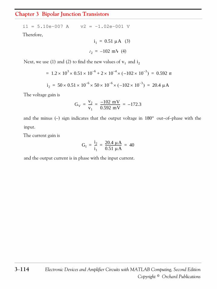
Chapter 3 Bipolar Junction Transistors
3−114 Electronic Devices and Amplifier Circuits with MATLAB Computing, Second EditionCopyright © Orchard Publications
i1 = 5.10e-007 A v2 = -1.02e-001 V
Therefore, (3)
(4)
Next, we use (1) and (2) to find the new values of and
The voltage gain is
and the minus (−) sign indicates that the output voltage in out−of−phase with the
input.
The current gain is
and the output current is in phase with the input current.
i1 0.51 μA=
v2 102 mV–=
v1 i2
1.2 103× 0.51 10 6–×× 2 10 4–× 102 10 3–×–( )×+ 0.592 m= =
i2 50 0.51 10 6–×× 50 10 6–×× 102 10 3–×–( )× 20.4 μA= =
GVv2
v1----- 102 mV–
0.592 mV------------------------- 172.3–= = =
180°
GIi2
i1--- 20.4 μA
0.51 μA-------------------- 40= = =

Electronic Devices and Amplifier Circuits with MATLAB Computing, Second Edition 4−1Copyright © Orchard Publications
Chapter 4
Field Effect Transistors and PNPN Devices
his chapter begins with a discussion of Field Effect Transistors (FETs), characteristics, andapplications. Other PNPN devices, the four−layer diode, the silicon controlled rectifier(SCR), the silicon controlled switch (SCS), and the triac are introduced with some of their
applications. The chapter includes also a brief discussion on unijunction transistors, and diacs.
4.1 The Junction Field Effect Transistor (JFET)
The Field−Effect Transistor (FET) is another semiconductor device. The Junction FET (JFET) isthe earlier type and the Metal Oxide Semiconductor FET (MOSFET) is now the most popular type.In this section we will discuss the JFET and we will discuss the MOSFET in the next section.
Figure 4.1(a) shows the basic JFET amplifier configuration and the output volt−ampere character-istics are shown in Fig. 4.1(b). These characteristics are similar to those for the junction transistorexcept that the parameter for this family is the input voltage rather than the input current. Likethe old vacuum triode, the FET is a voltage−controlled device.
Figure 4.1. Pictorial representation and output volt−ampere characteristics for a typical JFET
The lower terminal in the N material is called the source, and the upper terminal is called thedrain; the two regions of P material, which are usually connected together externally, are calledgates. P−N junctions exist between the P and N materials, and in normal operation the voltageapplied to the gates biases these junctions in the reverse direction. A potential barrier exists acrossthe junctions, and the electrons carrying the current in the N material are forced to flowthrough the channel between the two gates. If the voltage applied to the gates is changed, thewidth of the transition region at the junction changes; thus the width of the channel changes,resulting in a change in the resistance between source and drain. In this way the current in the
T
N
PP+
+
−
−vG
RL
VDD
Rs
vs
vD
iG
iD
10 20
iD mA( )15
12
9
6
3
vD V( )
a( )
vG 0=
vG 1–=
vG 2–=
vG 3–=
vG 4–=
b( )
iD

Chapter 4 Field Effect Transistors and PNPN Devices
4−2 Electronic Devices and Amplifier Circuits with MATLAB Computing, Second EditionCopyright © Orchard Publications
output circuit is controlled by the gate voltage. A small potential applied to the gates, 5 to 10volts, is sufficient to reduce the channel width to zero and to cut off the flow of current in theoutput circuit.
One of the most attractive features of the JFET is the fact that the input resistance, measuredbetween gate and source, can be made very large, from 1 to 100 megohms. This high input resis-tance results from the fact that the input voltage biases the junctions in the reverse directionand consequently is required to deliver only the small leakage current across the junctions. Thereare many circuits in which a high input resistance is required, and the ordinary junction transis-tor is not suitable for such applications.
JFETs have been made with input resistances exceeding 1 megohm, with transconductances inthe range of to millimhos, and with the ability to provide a voltage amplification of about at frequencies up to . The current in a JFET is carried only by majority carriers and forthis reason the FET is also known as unipolar transistor, in contrast to the ordinary transistor inwhich both majority and minority carriers participate in the conduction process, and it is knownas bipolar transistor.
To better understand the JFET operation, let us review the depletion region which we discussedin Chapter 2. Figure 4.2 shows a PN junction and the depletion region when no bias is applied.
Figure 4.2. PN junction and depletion region of a typical PN junction
The width of the depletion region depends on the applied bias. Forward−biasing, where a voltagesource is connected with the plus (+) on the P side and the minus (−) on the N side, makes thedepletion region narrower by repelling the holes and free electrons toward the junction, and ifthe bias is about , the free electrons will cross the junction and join with the holes. Thus,the forward biasing causes the depletion region to decrease resulting in a low resistance at thejunction and a relatively large current across it.
If a reverse−biasing is applied, where a voltage source is connected with the plus (+) on the Nside and the minus (−) on the P side, the free electrons move towards the right side while theholes move towards the left side causing the depletion region to widen. A high resistancebetween the terminals is developed, and only a small current flows between the terminals.
vG
1 5 1010 MHz
Junction
Depletion Region
HoleFree ElectronNegative Ion
Positive Ion
P N
0.65 V

Electronic Devices and Amplifier Circuits with MATLAB Computing, Second Edition 4−3Copyright © Orchard Publications
The Junction Field Effect Transistor (JFET)
The cross−sectional area of a typical JFET channel can be controlled by variations in the voltageapplied to the gate. This is illustrated in Figure 4.3.
Figure 4.3. JFET operation with adjustable gate bias
In Figure 4.3, let us adjust the voltage source at the gate so that , that is, the gate isgrounded, and set the voltage at the drain to . Let us assume that under those condi-tions the drain−to−source current through the channel is .Therefore, we concludethat the drain−to−source resistance is or .
Next, let us adjust the voltage source at the gate so that , and maintain the voltageat the drain to . This reverse−bias condition cause the depletion region to expandand that reduces the effective cross−sectional area of the channel. Let us assume that under thoseconditions the drain−to−source current through the channel is .Therefore, we con-clude that the drain−to−source resistance is now or .
Now, let us adjust the voltage source at the gate so that , and maintain the voltage atthe drain to . This reverse−bias condition cause the depletion region to expand evenmore and that reduces further the effective cross−sectional area of the channel. and we assumethat under those conditions the drain−to−source current through the channel is
.Thus, we conclude that the drain−to−source resistance is now or , and therefore, we observe that the drain−to−source
resistance can be controlled by the voltage applied at the gate. The voltage at the gate whichcauses the drain−to−source resistance to become infinite, is referred to as the pinch−off volt-age and it is denoted as . In other words, when , no current flows through the chan-nel.
N
PPGate G( )
Drain D( )
Source S( )
Depletion region
VDD
+
−VGG
+
−
VGG 0=
VDD 10 V=
IDS 10 mA=
RDS RDS VDD IDS⁄ 10 V 10 mA⁄= = RDS 1 KΩ=
VGG 2 V–=
VDD 10 V=
IDS 0.1 mA=
RDS RDS 10 V 0.1 mA⁄= RDS 100 KΩ=
VGG 4 V–=
VDD 10 V=
IDS 0.01 mA= RDS
RDS 10 V 0.01 mA⁄= RDS 1 MΩ=
RDS
RDS
VP VGG VP=
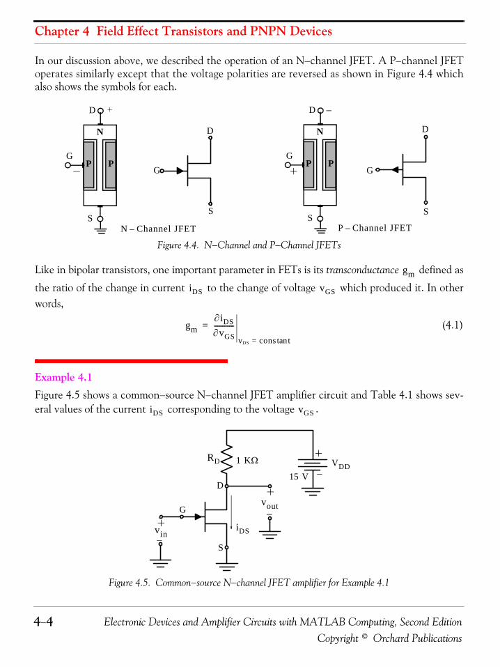
Chapter 4 Field Effect Transistors and PNPN Devices
4−4 Electronic Devices and Amplifier Circuits with MATLAB Computing, Second EditionCopyright © Orchard Publications
In our discussion above, we described the operation of an N−channel JFET. A P−channel JFEToperates similarly except that the voltage polarities are reversed as shown in Figure 4.4 whichalso shows the symbols for each.
Figure 4.4. N−Channel and P−Channel JFETs
Like in bipolar transistors, one important parameter in FETs is its transconductance defined as
the ratio of the change in current to the change of voltage which produced it. In otherwords,
(4.1)
Example 4.1 Figure 4.5 shows a common−source N−channel JFET amplifier circuit and Table 4.1 shows sev-eral values of the current corresponding to the voltage .
Figure 4.5. Common−source N−channel JFET amplifier for Example 4.1
N
PPG
D
S
+
D
S
G
N
PPG
D
S
+
D
S
G
−
N Channel JFET– P Channel JFET–
gm
iDS vGS
gm∂iDS∂vGS------------
vDS cons ttan=
=
iDS vGS
D
S
G
VDDRD 1 KΩ
vin
vout
+
−
iDS
+
+−
−
15 V

Electronic Devices and Amplifier Circuits with MATLAB Computing, Second Edition 4−5Copyright © Orchard Publications
The Junction Field Effect Transistor (JFET)
a. Find the output voltage if the input signal is .
b. Find the output voltage if the input signal is .
c. Is this an inverting or a non−inverting amplifier?
d. Find the transconductance using the results of (a) and (b).
e. Plot versus and indicate how the transconductance can be calculated from this plot.
Solution:a.
Figure 4.6. Circuit for the solution of Example 4.1From Figure 4.6,
(4.2)
but we do not know all values of for the interval . Therefore, let us use thefollowing MATLAB script to plot a suitable curve for this interval.
vGS=[−4 −3 −2 −1 0]; iDS=[0 2 8 20 35];... % These are the data in Table 4.1curve=polyfit(vGS,iDS,4);... % Fits the data to a polynomial of fourth degreevGSaxis=−4.0:0.1:0.0;... % Creates horizontal (vGS) axispolcurve=polyval(curve,vGSaxis);... % Computes the polynomial for vGS axis valuesplot(vGSaxis,polcurve);... % Plots the fourth degree polynomialxlabel('vGS (volts)'); ylabel('iDS (milliamps)'); title('Plot for Example 4.1'); grid
The generated plot is shown in Figure 4.7.
TABLE 3.1 Current versus voltage for Example 4.1iDS vGS
vGS V( ) 0 1– 2– 3– 4–
iDS mA( ) 35 20 8 2 0
vout vin 2.4 V–=
vout vin 1.8 V–=
iDS vGS
D
S
G
15 V
RD 1 KΩ
vin vGS=
vout
+
−
iDS
+
+−
−
VDD
vout VDD RDiDS–=
iDS 0 iDS 35 mA≤ ≤

Chapter 4 Field Effect Transistors and PNPN Devices
4−6 Electronic Devices and Amplifier Circuits with MATLAB Computing, Second EditionCopyright © Orchard Publications
Figure 4.7. MATLAB generated plot for Example 4.1
From the plot of Figure 4.7 we see that for , . Therefore,
(4.3)
b.From the plot of Figure 4.7 we see that for , . Therefore,
(4.4)
c.The results of (a) and (b) indicate that an increase in the input voltage results in a decrease ofthe output voltage. Therefore, we conclude that the given JFET circuit is an inverting ampli-fier.
d.(4.5)
e.The plot in Figure 4.7 shows the slope of and it is calculated as in (4.5).
4.2 The Metal Oxide Semiconductor Field Effect Transistor (MOSFET)The most popular type of a FET is the Metal−Oxide−Semiconductor Field Effect Transistor orMOSFET. Another less frequently name for the MOSFET is Insulated−Gate FET or IGFET.
-4 -3.5 -3 -2.5 -2 -1.5 -1 -0.5 0-5
0
5
10
15
20
25
30
35
vGS (volts)
iDS
(m
illia
mps
)
Plot for Example 4.1
vin vGS 2.4 V–= = iDS 5 mA≈
vout vGS 2.4 V–=VDD RDiDS– 15 103 5 10 3–××– 10 V= = =
vin vGS 1.8 V–= = iDS 10 mA≈
vout vGS 1.8 V–=VDD RDiDS– 15 103 10 10 3–××– 5 V= = =
gmΔiDSΔvGS------------- 5 10–( ) 10 3–×
2.4– 1.8–( )–------------------------------------- 0.0083 Ω 1–
= = =
gm

Electronic Devices and Amplifier Circuits with MATLAB Computing, Second Edition 4−7Copyright © Orchard Publications
The Metal Oxide Semiconductor Field Effect Transistor (MOSFET)
Figure 4.8 shows a cross section and the symbol for an −channel MOSFET or NMOS FETdevice. The complementary −channel MOSFET or PMOS FET is similar but opposite in polar-ity.
Figure 4.8. Cross section of an n−channel MOSFET
In Figure 4.8, heavily doped N−type regions, indicated by , are diffused into a P−type substrateor base. An conducting channel may be formed and exist with the gate voltage . A neg-ative gate voltage will then drive electrons out of the channel, increasing the resistance fromsource to drain. This is termed depletion−mode operation. The JFET also operates in this manner.Conversely, if no channel exists with , one can be formed by applying positive voltage and attracting electrons to a thin surface layer. This is termed enhancement−mode operation. Theenhancement mode MOSFET has a lightly doped channel and uses forward bias to enhance thecurrent carriers in the channel. A MOSFET can be constructed that will operate in either modedepending upon what type of bias is applied, thus allowing a greater range of input signals.
The symbols for the four basic variations of the MOSFET are shown in Figure 4.9.
Figure 4.9. MOSFET types and symbols
np
n+n+
L
wOX
Metal
p type substrate–
Substrate B( )
Source S( )Drain D( )
Gate G( )
Channel
n+
n VG 0=
VG 0= VG
G
D
B
S
G
D
B
S
Enhancement MOSFETn channel– p channel–
G
D
B
S
G
D
B
S
Depletion MOSFET
n channel– p channel–

Chapter 4 Field Effect Transistors and PNPN Devices
4−8 Electronic Devices and Amplifier Circuits with MATLAB Computing, Second EditionCopyright © Orchard Publications
4.2.1 The N−Channel MOSFET in the Enhancement Mode
Figure 4.10 shows the drain−to−source current versus the drain−to−source voltage fordifferent values of gate−to−source voltage .
Figure 4.10. Current−voltage characteristics for typical MOSFET
The voltage at which the channel is closed is known as the pinch−off voltage , and the mini-mum voltage required to form a conducting channel between the drain and source is referred toas the threshold voltage and it is denoted as . Typical values for are 2 to 4 volts for highvoltage devices with thicker gate oxides, and 1 to 2 volts for lower voltage devices with thinnergate oxides. In terms of this, the drain current in a MOSFET can be written approximately as
(4.6)
where is the channel length as shown in Figure 4.8, is the width of the structure perpendic-ular to the paper in Figure 4.8, is the oxide thickness, is its dielectric constant, and isthe mobility of carriers in the channel. The values for the channel length and width depend onthe voltage and typical values are and .
It is convenient to represent the quantity as *, and typical values of are around
. Then (4.6) is expressed as
(4.7)
* The subscript is used here as a reminder that relation (4.7) applies to n−channel MOSFETs.
iDS vDS
vGS
5 10
iDS mA( )
2.5
2.0
1.5
1.0
0.5
vDS V( )
vGS 5 V=
vGS 4 V=
vGS 3 V=
vGS 2 V=
vGS 1 V=
0
VP
VT VT
iD
iDεμWLwOX-------------- vGS VT–( )vDS
12---vDS
2–= for vDS vGS VT–≤
L WwOX ε μ
vGS 2 μm L 10 μm≤ ≤ 100 μm W 100 μm≤ ≤
εμ wOX⁄ kn kn
n
20 μA V2⁄
iD knWL----- vGS VT–( )vDS
12---vDS
2–= for vDS vGS VT–≤
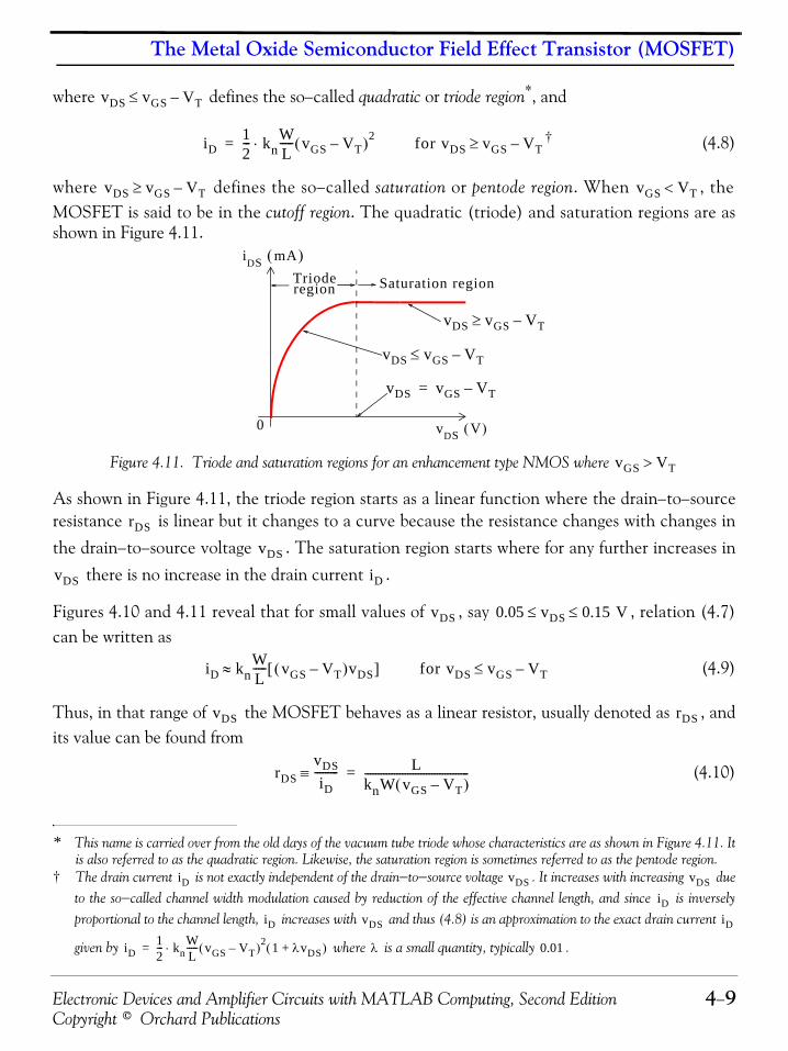
Electronic Devices and Amplifier Circuits with MATLAB Computing, Second Edition 4−9Copyright © Orchard Publications
The Metal Oxide Semiconductor Field Effect Transistor (MOSFET)
where defines the so−called quadratic or triode region*, and
† (4.8)
where defines the so−called saturation or pentode region. When , theMOSFET is said to be in the cutoff region. The quadratic (triode) and saturation regions are asshown in Figure 4.11.
Figure 4.11. Triode and saturation regions for an enhancement type NMOS where
As shown in Figure 4.11, the triode region starts as a linear function where the drain−to−sourceresistance is linear but it changes to a curve because the resistance changes with changes inthe drain−to−source voltage . The saturation region starts where for any further increases in
there is no increase in the drain current .
Figures 4.10 and 4.11 reveal that for small values of , say , relation (4.7)can be written as
(4.9)
Thus, in that range of the MOSFET behaves as a linear resistor, usually denoted as , andits value can be found from
(4.10)
* This name is carried over from the old days of the vacuum tube triode whose characteristics are as shown in Figure 4.11. Itis also referred to as the quadratic region. Likewise, the saturation region is sometimes referred to as the pentode region.
† The drain current is not exactly independent of the drain−to−source voltage . It increases with increasing dueto the so−called channel width modulation caused by reduction of the effective channel length, and since is inverselyproportional to the channel length, increases with and thus (4.8) is an approximation to the exact drain current
given by where is a small quantity, typically .
vDS vGS VT–≤
iD12--- kn
WL-----⋅ vGS VT–( )2= for vDS vGS VT–≥
iD vDS vDS
iD
iD vDS iD
iD12--- kn
WL-----⋅ vGS VT–( )2 1 λvDS+( )= λ 0.01
vDS vGS VT–≥ vGS VT<
iDS mA( )
vDS V( )0
Saturation regionregionTriode
vDS vGS VT–=
vDS vGS VT–≥
vDS vGS VT–≤
vGS VT>
rDS
vDS
vDS iD
vDS 0.05 vDS 0.15 V≤ ≤
iD knWL----- vGS VT–( )vDS[ ]≈ for vDS vGS VT–≤
vDS rDS
rDSvDSiD
---------≡ LknW vGS VT–( )---------------------------------------=
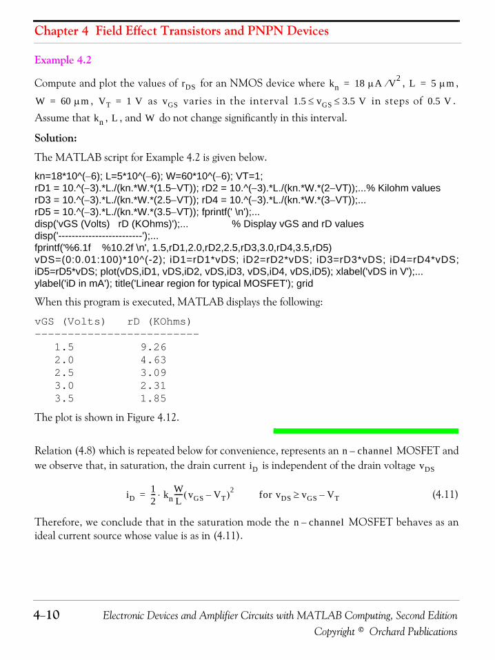
Chapter 4 Field Effect Transistors and PNPN Devices
4−10 Electronic Devices and Amplifier Circuits with MATLAB Computing, Second EditionCopyright © Orchard Publications
Example 4.2
Compute and plot the values of for an NMOS device where , ,
, as varies in the interval in steps of .Assume that , , and do not change significantly in this interval.
Solution:
The MATLAB script for Example 4.2 is given below.
kn=18*10^(−6); L=5*10^(−6); W=60*10^(−6); VT=1;rD1 = 10.^(−3).*L./(kn.*W.*(1.5−VT)); rD2 = 10.^(−3).*L./(kn.*W.*(2−VT));...% Kilohm valuesrD3 = 10.^(−3).*L./(kn.*W.*(2.5−VT)); rD4 = 10.^(−3).*L./(kn.*W.*(3−VT));...rD5 = 10.^(−3).*L./(kn.*W.*(3.5−VT)); fprintf(' \n');...disp('vGS (Volts) rD (KOhms)');... % Display vGS and rD valuesdisp('-------------------------');...fprintf('%6.1f %10.2f \n', 1.5,rD1,2.0,rD2,2.5,rD3,3.0,rD4,3.5,rD5)vDS=(0:0.01:100)*10^(-2); iD1=rD1*vDS; iD2=rD2*vDS; iD3=rD3*vDS; iD4=rD4*vDS;iD5=rD5*vDS; plot(vDS,iD1, vDS,iD2, vDS,iD3, vDS,iD4, vDS,iD5); xlabel('vDS in V');...ylabel('iD in mA'); title('Linear region for typical MOSFET'); grid
When this program is executed, MATLAB displays the following:
vGS (Volts) rD (KOhms)------------------------- 1.5 9.26 2.0 4.63 2.5 3.09 3.0 2.31 3.5 1.85
The plot is shown in Figure 4.12.
Relation (4.8) which is repeated below for convenience, represents an MOSFET andwe observe that, in saturation, the drain current is independent of the drain voltage
(4.11)
Therefore, we conclude that in the saturation mode the MOSFET behaves as anideal current source whose value is as in (4.11).
rDS kn 18 μA V2⁄= L 5 μm=
W 60 μm= VT 1 V= vGS 1.5 vGS 3.5 V≤ ≤ 0.5 V
kn L W
n channel–
iD vDS
iD12--- kn
WL-----⋅ vGS VT–( )2
= for vDS vGS VT–≥
n channel–

Electronic Devices and Amplifier Circuits with MATLAB Computing, Second Edition 4−11Copyright © Orchard Publications
The Metal Oxide Semiconductor Field Effect Transistor (MOSFET)
Figure 4.12. Plot for Example 4.2
In analogy with the transconductance in bipolar junction transistors, the MOSFET transconduc-tance is defined as
(4.12)
In other words, the transconductance is a measure of the sensitivity of drain current to changes ingate−to−source bias.
As indicated in the previous chapter, subscripts in upper case represent the sum of the quiescentand small signal parameters, and subscripts in lower case represent just the small signal parame-ters. Thus, and (4.11) can be expressed as
For small signals, transconductance is defined in terms of the second term of the above expressionand thus
Letting
and substituting the last expression above into (4.12) we obtain
0 0.2 0.4 0.6 0.8 10
2
4
6
8
10
vDS in V
iD in
mA
Linear region for typical MOSFET
VGS 1.5 V=VGS 2.0 V=VGS 2.5 V=
VGS 3.0 V=
VGS 3.5 V=
gm∂iD
∂vGS------------
vDS cons ttan=
=
vGS VGS vgs+=
iD12--- kn
WL-----⋅ VGS vgs VT–+( )2 1
2--- kn
WL-----⋅ VGS VT–( ) vgs+[ ]2
= =
12--- kn
WL-----⋅ VGS VT–( )2 kn
WL----- VGS VT–( )vgs
12--- kn
WL-----⋅ vgs
2+ +=
id knWL----- VGS VT–( )vgs=
∂id∂vgs-----------
id2 id1–
vgs2 vgs1–---------------------------
idvgs-------= =

Chapter 4 Field Effect Transistors and PNPN Devices
4−12 Electronic Devices and Amplifier Circuits with MATLAB Computing, Second EditionCopyright © Orchard Publications
(4.13)
or(4.14)
The output conductance is defined as
(4.15)
At saturation the slope of (4.15) is(4.16)
From (4.7) for the triode region
Therefore the output conductance is found by differentiation of the last expression above as
(4.17)
4.2.2 The N−Channel MOSFET in the Depletion Mode
As we’ve learned, in the enhancement mode we apply a positive voltage and as this valueincreases, the channel conductivity increases until we reach saturation. However, a MOSFETcan also be fabricated with an implanted channel so that drain current will flow if we apply avoltage even though the voltage is zero. If, however we want to decrease the channelconductivity, we can apply a sufficiently negative to deplete the implanted channel, and thismode of operation is referred to as the depletion mode. The negative value of that causes thechannel to be entirely depleted is the threshold voltage of the MOSFET andobviously has a negative value. At this threshold negative voltage , the drain current iszero although may still be present.
Typical values of drain current versus the gate−to−source voltage characteristics for an MOSFET that operates in the enhancement mode only are shown in Figure 4.13(a)
and one that operates in both the depletion and enhancement modes are shown in Figure4.13(b).
gmid
vgs-------
kn W L⁄( ) VGS VT–( )vgsvgs
-------------------------------------------------------------= =
gmid
vgs------- kn
WL----- VGS VT–( )= =
go∂iD
∂vDS------------
vGS cons ttan=
=
go sat( ) 0=
iD knWL----- vGS VT–( )vDS
12---vDS
2–=
go∂iD
∂vDS------------ kn
WL----- vGS VT– vDS–( )= =
vGS
iD
vDS vGS
vGS
vGS
VT n channel–
VT iD
vDS
iD vGS
n channel–
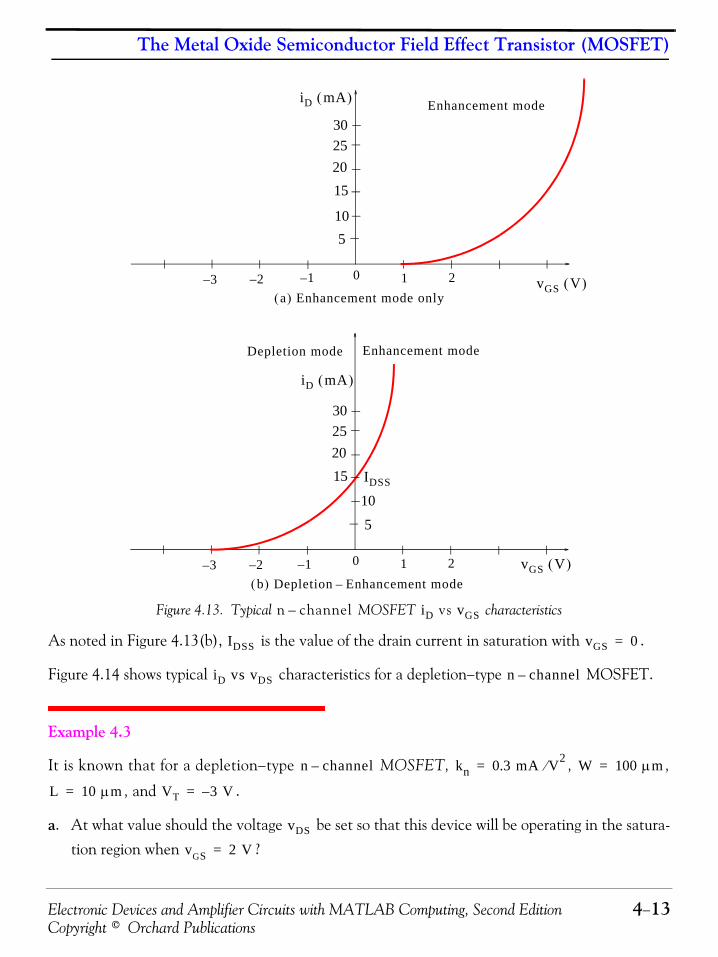
Electronic Devices and Amplifier Circuits with MATLAB Computing, Second Edition 4−13Copyright © Orchard Publications
The Metal Oxide Semiconductor Field Effect Transistor (MOSFET)
Figure 4.13. Typical MOSFET characteristics
As noted in Figure 4.13(b), is the value of the drain current in saturation with .
Figure 4.14 shows typical characteristics for a depletion−type MOSFET.
Example 4.3
It is known that for a depletion−type MOSFET, , ,
, and .
a. At what value should the voltage be set so that this device will be operating in the satura-tion region when ?
5
0
15
10
1
302520
23– 2– 1–
5
0
15
10
1
302520
23– 2– 1–
vGS V( )
iD mA( )
iD mA( )
vGS V( )
Enhancement mode
Enhancement modeDepletion mode
a( ) Enhancement mode only
b( ) Depletion Enhancement mode–
IDSS
n channel– iD vs vGS
IDSS vGS 0=
iD vs vDS n channel–
n channel– kn 0.3 mA V2⁄= W 100 μm=
L 10 μm= VT 3 V–=
vDS
vGS 2 V=
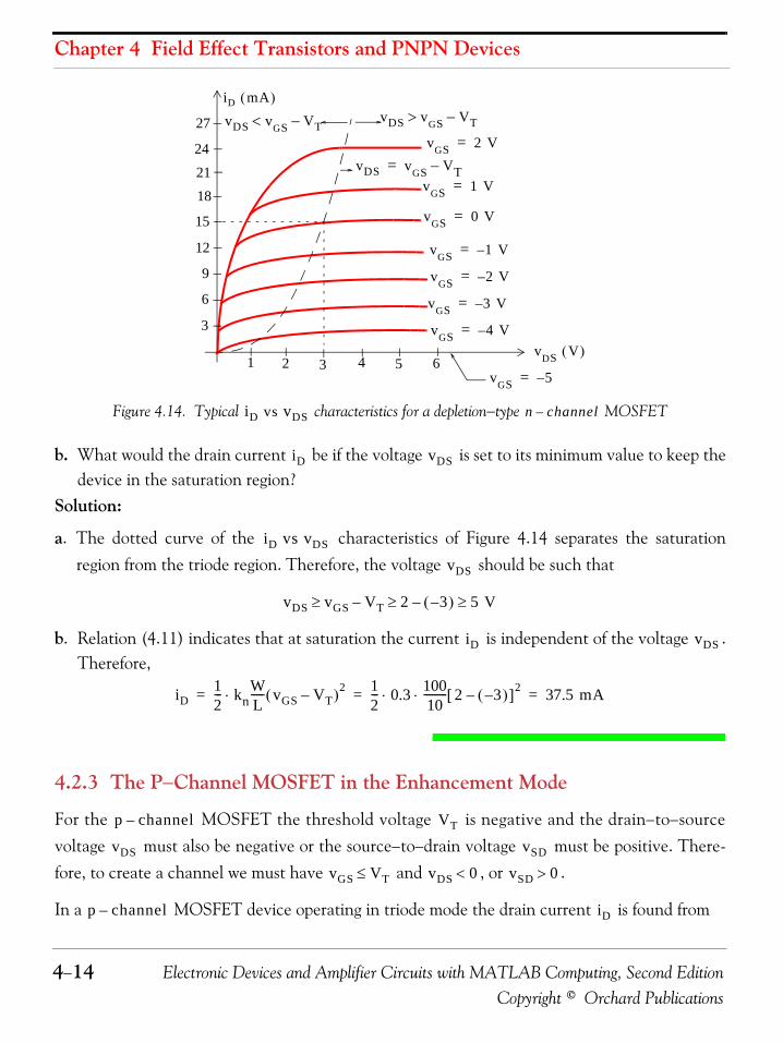
Chapter 4 Field Effect Transistors and PNPN Devices
4−14 Electronic Devices and Amplifier Circuits with MATLAB Computing, Second EditionCopyright © Orchard Publications
Figure 4.14. Typical characteristics for a depletion−type MOSFET
b. What would the drain current be if the voltage is set to its minimum value to keep thedevice in the saturation region?
Solution:
a. The dotted curve of the characteristics of Figure 4.14 separates the saturationregion from the triode region. Therefore, the voltage should be such that
b. Relation (4.11) indicates that at saturation the current is independent of the voltage .Therefore,
4.2.3 The P−Channel MOSFET in the Enhancement Mode
For the MOSFET the threshold voltage is negative and the drain−to−sourcevoltage must also be negative or the source−to−drain voltage must be positive. There-fore, to create a channel we must have and , or .
In a MOSFET device operating in triode mode the drain current is found from
1 6
iD mA( )
15
12
9
6
3
vDS V( )
vGS 0 V=
vGS 1 V–=
vGS 2 V–=
vGS 3 V–=
vGS 4 V–=
27
242118
vGS 5–=
vGS 1 V=
vGS 2 V=
2 3 4 5
vDS vGS VT–>vDS vGS VT–<
vDS vGS VT–=
iD vs vDS n channel–
iD vDS
iD vs vDS
vDS
vDS vGS VT– 2 3–( )– 5 V≥ ≥ ≥
iD vDS
iD12--- kn
WL-----⋅ vGS VT–( )2 1
2--- 0.3 100
10--------- 2 3–( )–[ ]2⋅ ⋅ 37.5 mA= = =
p channel– VT
vDS vSD
vGS VT≤ vDS 0< vSD 0>
p channel– iD
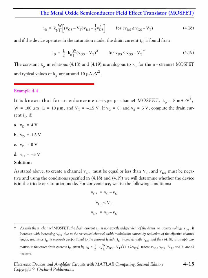
Electronic Devices and Amplifier Circuits with MATLAB Computing, Second Edition 4−15Copyright © Orchard Publications
The Metal Oxide Semiconductor Field Effect Transistor (MOSFET)
(4.18)
and if the device operates in the saturation mode, the drain current is found from
* (4.19)
The constant in relations (4.18) and (4.19) is analogous to for the MOSFET
and typical values of are around .
Example 4.4
I t i s known that for an enhancement− type MOSFET, ,
, , and . If , and , compute the drain cur-rent if:
a.
b.
c.
d.
Solution:
As stated above, to create a channel must be equal or less than , and must be nega-tive and using the conditions specified in (4.18) and (4.19) we will determine whether the deviceis in the triode or saturation mode. For convenience, we list the following conditions:
* As with the n−channel MOSFET, the drain current is not exactly independent of the drain−to−source voltage . Itincreases with increasing due to the so−called channel width modulation caused by reduction of the effective channellength, and since is inversely proportional to the channel length, increases with and thus (4.18) is an approxi-
mation to the exact drain current given by where , , , and are all
negative.
iD kpWL----- vGS VT–( )vDS
12---vDS
2–= for vDS vGS VT–≥( )
iD
iD12--- kp
WL-----⋅ vGS VT–( ) 2= for vDS vGS VT–≤
iD vDS
vDS
iD iD vDS
iD iD12--- kn
WL-----⋅ vGS VT–( )2 1 λvDS+( )= vGS vDS VT λ
kp kn n channel–
kp 10 μA V2⁄
p channel– kp 8 mA V2⁄=
W 100 μm= L 10 μm= VT 1.5 V–= vG 0= vS 5 V=
iD
vD 4 V=
vD 1.5 V=
vD 0 V=
vD 5– V=
vGS VT vDS
vGS vG vS–=
vGS VT<
vDS vD vS–=

Chapter 4 Field Effect Transistors and PNPN Devices
4−16 Electronic Devices and Amplifier Circuits with MATLAB Computing, Second EditionCopyright © Orchard Publications
a.
and we conclude that the device operates in the triode mode. Then, with (4.17) we obtain
b.
and we conclude that the device operates at the point where the triode mode ends and thesaturation region begins. Then, with (4.19) we obtain
c.
and we conclude that the device operates well in the saturation region.Then, with (4.19) weobtain
d.
vDS vGS VT–>
vGS vG vS– 0 5– 5 V–= = =
vGS VT< 5 1.5 –<–⇒
vDS vD vS– 4 5– 1 V–= = =
vGS VT– 5– 1.5–( )– 3.5 V–= =
vDS vGS VT–> 1 3.5–>–⇒
iD kpWL----- vGS VT–( )vDS
12---vDS
2– 8 10
1------ 5– 1.5–( )–( ) 1–( )×[ ]×× 0.5 1–( ) 2×– 0.24 mA= = =
vDS vD vS– 1.5 5– 3.5 V–= = =
vGS VT– 5– 1.5–( )– 3.5 V–= =
vDS vGS VT– 3.5 V–= =
iD12--- kp
WL-----⋅ vGS VT–( ) 2 0.5 8 10 5– 1.5–( )–[ ] 2×× 0.49 mA= = =
vDS vD vS– 0 5– 5 V–= = =
vGS VT– 5– 1.5–( )– 3.5 V–= =
vDS vGS VT–< 5 3.5<–⇒
iD12--- kp
WL-----⋅ vGS VT–( ) 2 0.5 8 10 5– 1.5–( )–[ ] 2×× 0.49 mA= = =
vDS vD vS– 5– 5– 10 V–= = =
vGS VT– 5– 1.5–( )– 3.5 V–= =
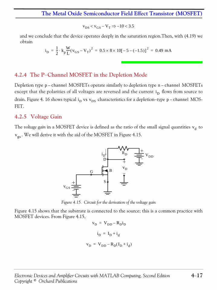
Electronic Devices and Amplifier Circuits with MATLAB Computing, Second Edition 4−17Copyright © Orchard Publications
The Metal Oxide Semiconductor Field Effect Transistor (MOSFET)
and we conclude that the device operates deeply in the saturation region.Then, with (4.19) weobtain
4.2.4 The P−Channel MOSFET in the Depletion Mode
Depletion type MOSFETs operate similarly to depletion type MOSFETsexcept that the polarities of all voltages are reversed and the current flows from source to
drain. Figure 4. 16 shows typical characteristics for a depletion−type MOS-FET.
4.2.5 Voltage Gain
The voltage gain in a MOSFET device is defined as the ratio of the small signal quantities to
. We will derive it with the aid of the MOSFET in Figure 4.15.
Figure 4.15. Circuit for the derivation of the voltage gain
Figure 4.15 shows that the substrate is connected to the source; this is a common practice withMOSFET devices. From Figure 4.15,
vDS vGS VT–< 10 3.5<–⇒
iD12--- kp
WL-----⋅ vGS VT–( ) 2 0.5 8 10 5– 1.5–( )–[ ] 2×× 0.49 mA= = =
p channel– n channel–
iDiD vs vDS p channel–
vd
vgs
DVDD
RD
vGS
vD
+
+
−
−
iD
G B
S
+
−
vD VDD RDiD–=
iD ID id+=
vD VDD RD ID id+( )–=
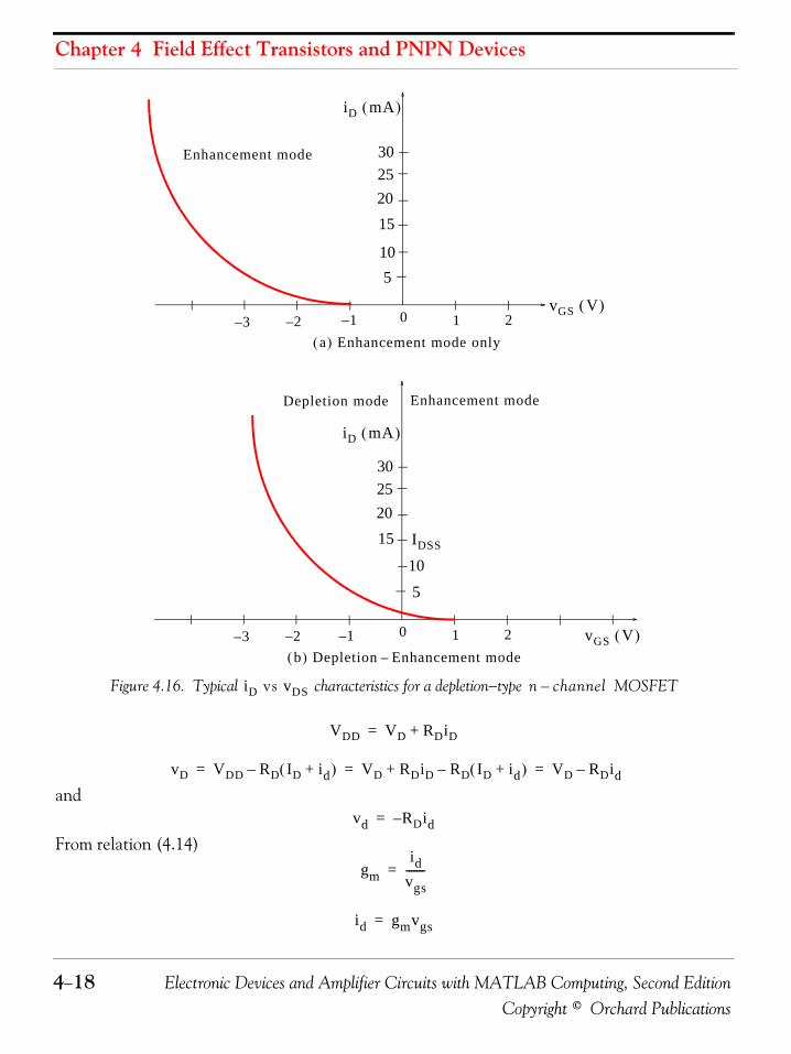
Chapter 4 Field Effect Transistors and PNPN Devices
4−18 Electronic Devices and Amplifier Circuits with MATLAB Computing, Second EditionCopyright © Orchard Publications
Figure 4.16. Typical characteristics for a depletion−type MOSFET
and
From relation (4.14)
5
0
15
10
1
302520
23– 2– 1–
5
0
15
10
1
302520
23– 2– 1–
vGS V( )
iD mA( )
iD mA( )
vGS V( )
Enhancement mode
Enhancement modeDepletion mode
a( ) Enhancement mode only
b( ) Depletion Enhancement mode–
IDSS
iD vs vDS n channel–
VDD VD RDiD+=
vD VDD RD ID id+( )– VD RDiD RD ID id+( )–+ VD RDid–= = =
vd RDid–=
gmid
vgs-------=
id gmvgs=
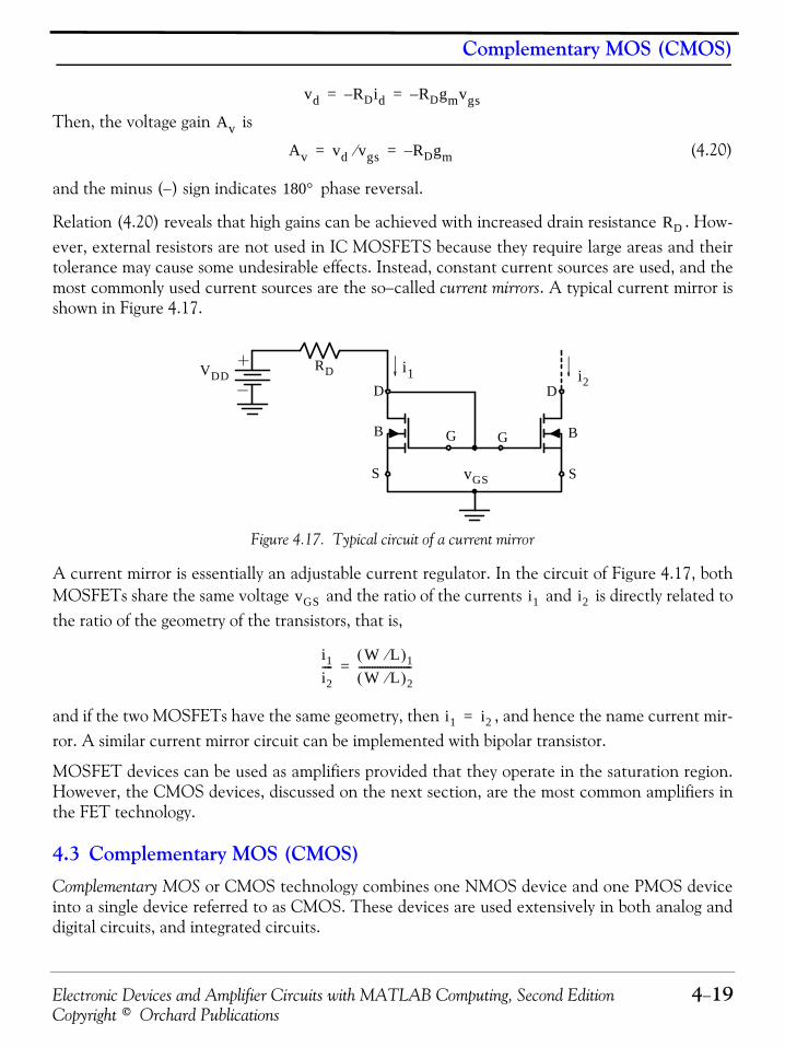
Electronic Devices and Amplifier Circuits with MATLAB Computing, Second Edition 4−19Copyright © Orchard Publications
Complementary MOS (CMOS)
Then, the voltage gain is
(4.20)
and the minus (−) sign indicates phase reversal.
Relation (4.20) reveals that high gains can be achieved with increased drain resistance . How-ever, external resistors are not used in IC MOSFETS because they require large areas and theirtolerance may cause some undesirable effects. Instead, constant current sources are used, and themost commonly used current sources are the so−called current mirrors. A typical current mirror isshown in Figure 4.17.
Figure 4.17. Typical circuit of a current mirror
A current mirror is essentially an adjustable current regulator. In the circuit of Figure 4.17, bothMOSFETs share the same voltage and the ratio of the currents and is directly related tothe ratio of the geometry of the transistors, that is,
and if the two MOSFETs have the same geometry, then , and hence the name current mir-ror. A similar current mirror circuit can be implemented with bipolar transistor.
MOSFET devices can be used as amplifiers provided that they operate in the saturation region.However, the CMOS devices, discussed on the next section, are the most common amplifiers inthe FET technology.
4.3 Complementary MOS (CMOS)Complementary MOS or CMOS technology combines one NMOS device and one PMOS deviceinto a single device referred to as CMOS. These devices are used extensively in both analog anddigital circuits, and integrated circuits.
vd RDid– RDgmvgs–= =
Av
Av vd vgs⁄ RDgm–= =
180°
RD
D
B
S
D
B
S vGS
i1 i2 VDD
RD
GG
vGS i1 i2
i1i2----
W L⁄( )1W L⁄( )2
--------------------=
i1 i2=
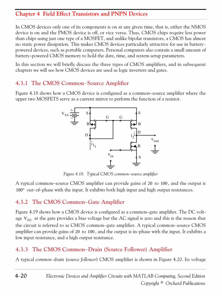
Chapter 4 Field Effect Transistors and PNPN Devices
4−20 Electronic Devices and Amplifier Circuits with MATLAB Computing, Second EditionCopyright © Orchard Publications
In CMOS devices only one of its components is on at any given time, that is, either the NMOSdevice is on and the PMOS device is off, or vice versa. Thus, CMOS chips require less powerthan chips using just one type of a MOSFET, and unlike bipolar transistors, a CMOS has almostno static power dissipation. This makes CMOS devices particularly attractive for use in battery−powered devices, such as portable computers. Personal computers also contain a small amount ofbattery−powered CMOS memory to hold the date, time, and system setup parameters.
In this section we will briefly discuss the three types of CMOS amplifiers, and in subsequentchapters we will see how CMOS devices are used as logic inverters and gates.
4.3.1 The CMOS Common−Source Amplifier
Figure 4.18 shows how a CMOS device is configured as a common−source amplifier where theupper two MOSFETS serve as a current mirror to perform the function of a resistor.
Figure 4.18. Typical CMOS common−source amplifier
A typical common−source CMOS amplifier can provide gains of to , and the output is out−of−phase with the input. It exhibits both high input and high output resistances.
4.3.2 The CMOS Common−Gate Amplifier
Figure 4.19 shows how a CMOS device is configured as a common−gate amplifier. The DC volt-age at the gate provides a bias voltage but the AC signal is zero and this is the reason thatthe circuit is referred to as CMOS common−gate amplifier. A typical common−source CMOSamplifier can provide gains of to , and the output is in−phase with the input. It exhibits alow input resistance, and a high output resistance.
4.3.3 The CMOS Common−Drain (Source Follower) Amplifier
A typical common−drain (source follower) CMOS amplifier is shown in Figure 4.20. Its voltage
S
B
D
S
B
D
i1 B
S
VSS
vout
vin
i2
G G
20 100180°
VDC
20 100

Electronic Devices and Amplifier Circuits with MATLAB Computing, Second Edition 4−21Copyright © Orchard Publications
The Metal Semiconductor FET (MESFET)
gain is less than unity, and the output is in−phase with the input. It exhibits a low output resis-tance, and thus it can be used as a buffer amplifier. It is referred to as common−drain amplifierbecause there is no signal at the drain of the upper MOSFET device; the voltage just pro-vides a bias. It is also referred to as source follower because the lower right MOSFET device acts asa load for the upper MOSFET device.
Figure 4.19. Typical CMOS common−gate amplifier
Figure 4.20. Typical common−drain (source follower) amplifier
4.4 The Metal Semiconductor FET (MESFET)The Metal−Semiconductor−Field−Effect−Transistor (MESFET) consists of a conducting channelpositioned between a source and drain contact region. The carrier flow from source to drain iscontrolled by a Schottky metal gate. The control of the channel is obtained by varying the deple-tion layer width underneath the metal contact which modulates the thickness of the conductingchannel and thereby the current. MESFETs use GaAs (gallium arsenide) technology. Only
VDD
S
D
S
B
Dvout
VDC
vin
G GVSS
B
D
B
S
D B
S
i1
VSS
Bvin
VDD
vout
i2
D
S
G G
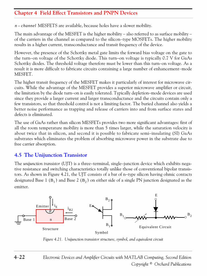
Chapter 4 Field Effect Transistors and PNPN Devices
4−22 Electronic Devices and Amplifier Circuits with MATLAB Computing, Second EditionCopyright © Orchard Publications
MESFETS are available, because holes have a slower mobility.
The main advantage of the MESFET is the higher mobility − also referred to as surface mobility −of the carriers in the channel as compared to the silicon−type MOSFETs. The higher mobilityresults in a higher current, transconductance and transit frequency of the device.
However, the presence of the Schottky metal gate limits the forward bias voltage on the gate tothe turn−on voltage of the Schottky diode. This turn−on voltage is typically 0.7 V for GaAsSchottky diodes. The threshold voltage therefore must be lower than this turn−on voltage. As aresult it is more difficult to fabricate circuits containing a large number of enhancement−modeMESFET.
The higher transit frequency of the MESFET makes it particularly of interest for microwave cir-cuits. While the advantage of the MESFET provides a superior microwave amplifier or circuit,the limitation by the diode turn−on is easily tolerated. Typically depletion−mode devices are usedsince they provide a larger current and larger transconductance and the circuits contain only afew transistors, so that threshold control is not a limiting factor. The buried channel also yields abetter noise performance as trapping and release of carriers into and from surface states anddefects is eliminated.
The use of GaAs rather than silicon MESFETs provides two more significant advantages: first ofall the room temperature mobility is more than 5 times larger, while the saturation velocity isabout twice that in silicon, and second it is possible to fabricate semi−insulating (SI) GaAssubstrates which eliminates the problem of absorbing microwave power in the substrate due tofree carrier absorption.
4.5 The Unijunction TransistorThe unijunction transistor (UJT) is a three−terminal, single−junction device which exhibits nega-tive resistance and switching characteristics totally unlike those of conventional bipolar transis-tors. As shown in Figure 4.21, the UJT consists of a bar of n−type silicon having ohmic contactsdesignated Base 1 ( ) and Base 2 ( ) on either side of a single PN junction designated as theemitter.
Figure 4.21. Unijunction transistor structure, symbol, and equivalent circuit
n channel–
B1 B2
p
n Base 2
SymbolEquivalent CircuitStructure
Emitter
B2
iE iB2
Base 1B1
E
B2B1
E
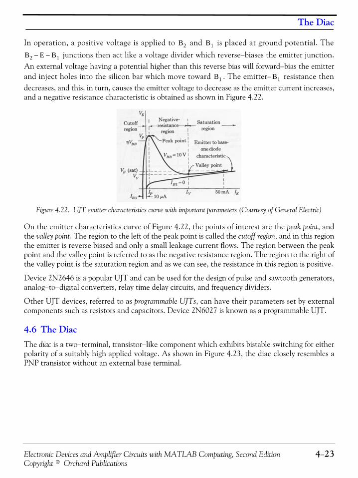
Electronic Devices and Amplifier Circuits with MATLAB Computing, Second Edition 4−23Copyright © Orchard Publications
The Diac
In operation, a positive voltage is applied to and is placed at ground potential. The junctions then act like a voltage divider which reverse−biases the emitter junction.
An external voltage having a potential higher than this reverse bias will forward−bias the emitterand inject holes into the silicon bar which move toward . The emitter− resistance thendecreases, and this, in turn, causes the emitter voltage to decrease as the emitter current increases,and a negative resistance characteristic is obtained as shown in Figure 4.22.
Figure 4.22. UJT emitter characteristics curve with important parameters (Courtesy of General Electric)
On the emitter characteristics curve of Figure 4.22, the points of interest are the peak point, andthe valley point. The region to the left of the peak point is called the cutoff region, and in this regionthe emitter is reverse biased and only a small leakage current flows. The region between the peakpoint and the valley point is referred to as the negative resistance region. The region to the right ofthe valley point is the saturation region and as we can see, the resistance in this region is positive.
Device 2N2646 is a popular UJT and can be used for the design of pulse and sawtooth generators,analog−to−digital converters, relay time delay circuits, and frequency dividers.
Other UJT devices, referred to as programmable UJTs, can have their parameters set by externalcomponents such as resistors and capacitors. Device 2N6027 is known as a programmable UJT.
4.6 The DiacThe diac is a two−terminal, transistor−like component which exhibits bistable switching for eitherpolarity of a suitably high applied voltage. As shown in Figure 4.23, the diac closely resembles aPNP transistor without an external base terminal.
B2 B1
B2 E– B1–
B1 B1
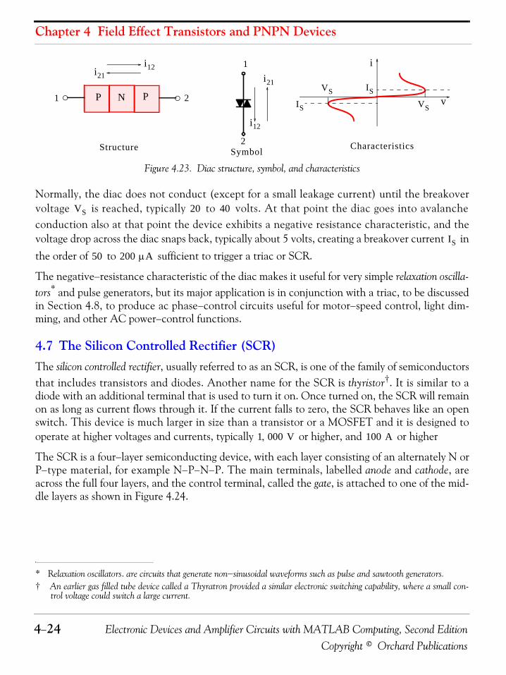
Chapter 4 Field Effect Transistors and PNPN Devices
4−24 Electronic Devices and Amplifier Circuits with MATLAB Computing, Second EditionCopyright © Orchard Publications
Figure 4.23. Diac structure, symbol, and characteristics
Normally, the diac does not conduct (except for a small leakage current) until the breakovervoltage is reached, typically to volts. At that point the diac goes into avalancheconduction also at that point the device exhibits a negative resistance characteristic, and thevoltage drop across the diac snaps back, typically about 5 volts, creating a breakover current inthe order of to sufficient to trigger a triac or SCR.
The negative−resistance characteristic of the diac makes it useful for very simple relaxation oscilla-tors* and pulse generators, but its major application is in conjunction with a triac, to be discussedin Section 4.8, to produce ac phase−control circuits useful for motor−speed control, light dim-ming, and other AC power−control functions.
4.7 The Silicon Controlled Rectifier (SCR)The silicon controlled rectifier, usually referred to as an SCR, is one of the family of semiconductorsthat includes transistors and diodes. Another name for the SCR is thyristor†. It is similar to adiode with an additional terminal that is used to turn it on. Once turned on, the SCR will remainon as long as current flows through it. If the current falls to zero, the SCR behaves like an openswitch. This device is much larger in size than a transistor or a MOSFET and it is designed tooperate at higher voltages and currents, typically or higher, and or higher
The SCR is a four−layer semiconducting device, with each layer consisting of an alternately N orP−type material, for example N−P−N−P. The main terminals, labelled anode and cathode, areacross the full four layers, and the control terminal, called the gate, is attached to one of the mid-dle layers as shown in Figure 4.24.
* Relaxation oscillators. are circuits that generate non−sinusoidal waveforms such as pulse and sawtooth generators.† An earlier gas filled tube device called a Thyratron provided a similar electronic switching capability, where a small con-
trol voltage could switch a large current.
NP P
2
1
1
2
i12
i21 i21
i
v
Structure Symbol Characteristics
VS
VS IS
IS
i12
VS 20 40
IS
50 200 μA
1 000 V, 100 A
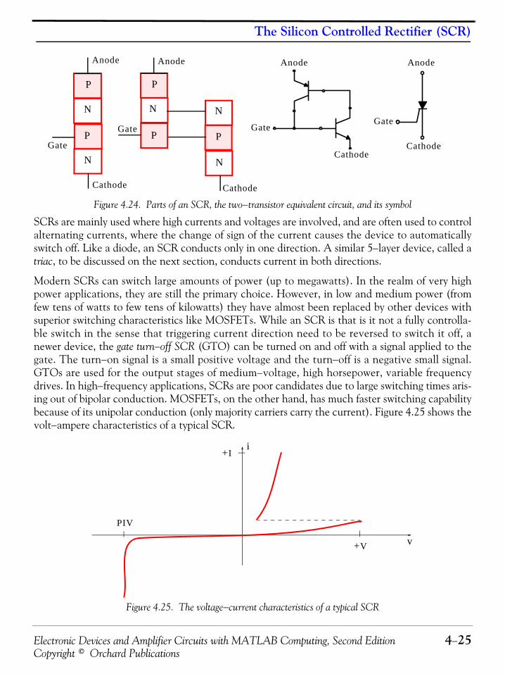
Electronic Devices and Amplifier Circuits with MATLAB Computing, Second Edition 4−25Copyright © Orchard Publications
The Silicon Controlled Rectifier (SCR)
Figure 4.24. Parts of an SCR, the two−transistor equivalent circuit, and its symbol
SCRs are mainly used where high currents and voltages are involved, and are often used to controlalternating currents, where the change of sign of the current causes the device to automaticallyswitch off. Like a diode, an SCR conducts only in one direction. A similar 5−layer device, called atriac, to be discussed on the next section, conducts current in both directions.
Modern SCRs can switch large amounts of power (up to megawatts). In the realm of very highpower applications, they are still the primary choice. However, in low and medium power (fromfew tens of watts to few tens of kilowatts) they have almost been replaced by other devices withsuperior switching characteristics like MOSFETs. While an SCR is that is it not a fully controlla-ble switch in the sense that triggering current direction need to be reversed to switch it off, anewer device, the gate turn−off SCR (GTO) can be turned on and off with a signal applied to thegate. The turn−on signal is a small positive voltage and the turn−off is a negative small signal.GTOs are used for the output stages of medium−voltage, high horsepower, variable frequencydrives. In high−frequency applications, SCRs are poor candidates due to large switching times aris-ing out of bipolar conduction. MOSFETs, on the other hand, has much faster switching capabilitybecause of its unipolar conduction (only majority carriers carry the current). Figure 4.25 shows thevolt−ampere characteristics of a typical SCR.
Figure 4.25. The voltage−current characteristics of a typical SCR
P
P
N
N
P
P
N
P
N
N
Anode
Cathode
Gate
Anode
Cathode
Gate
Anode
Gate
Cathode
Gate
Anode
Cathode
v
i
+V
+I
PIV

Chapter 4 Field Effect Transistors and PNPN Devices
4−26 Electronic Devices and Amplifier Circuits with MATLAB Computing, Second EditionCopyright © Orchard Publications
As shown in Figure 4.25, when the forward bias voltage from anode to cathode reaches a valueindicated as , and a positive signal is applied to the gate, the device reverts to a low imped-ance and current flows from the anode to cathode. The dotted line shows the interval of the volt-ages from anode to cathode in which the SCR will be conducting after the trigger signal has beenremoved. The current must be limited by the load to the value , or the SCR will be damaged.
When the forward bias from anode to cathode is reduced to zero or becomes negative, the SCRbecomes a non−conductive device and the signal at the gate, even if present, will not change thenon−conductive state of the device. If the negative bias exceeds the peak−inverse voltage indicatedas , the SCR will be damaged. It is recommended that the value should be at least threetimes the RMS value of the applied voltage.Figure 4.26 shows sinusoidal waveform applied to the gate of an SCR where during the positivehalf cycle the SCR is triggered at after the sinewave starts from zero and increases in the pos-itive direction.
Figure 4.26. SCR gate control
As shown in Figure 4.26, the number of degrees from the beginning of the cycle until the SCR isgated to the on condition is referred to as the firing angle, and the number of degrees that theSCR remains conducting is known as the conduction angle. For accurate SCR gating, the firingcircuit must be synchronized with the AC line voltage being applied anode−to−cathode acrossthe device. Without synchronization, the SCR firing would be random in nature and the systemresponse will be erratic. Also, when the firing angle is greater than zero, the voltage applied to theload is no longer sinusoidal. This presents no problem in the case of motor loads, but for radioand television an interference is created and usually the manufacturer of the SCR equipment willinclude an electromagnetic interference (EMI) filter to rectify the problem.
In closed−loop systems, such as motor control, an Error Detector Circuit computes the requiredfiring angle based on the system setpoint and the actual system output. The firing circuit is ableto sense the start of the cycle, and, based on an input from the Error Detector, delay the firingpulse until the proper time in the cycle to provide the desired output voltage. An analogy of a fir-ing circuit would be an automobile distributor which advances or retards the spark plug firingbased on the action of the vacuum advance mechanism.
In analog control systems the error detector circuit is usually an integrated circuit operational
+V
+I
PIV PIV
45°
θ Conductionangle
Firing angle
θ 45°=

Electronic Devices and Amplifier Circuits with MATLAB Computing, Second Edition 4−27Copyright © Orchard Publications
The Silicon Controlled Rectifier (SCR)
amplifier which takes reference and system feedback inputs and computes the amount of error(difference) between the actual output voltage and the desired setpoint value. Even though theSCR is an analog device, many new control systems now use a microprocessor based, digital, firingcircuit to sense the AC line zero−crossing, measure feedback and compare it with the setpoint,and generate the required firing angle to hold the system in a balanced state.
Another consideration is SCR protection. The SCR, like a conventional diode, has a very highone−cycle surge rating. Typically, the device will carry from eight to ten time its continuous cur-rent rating for a period of one electrical cycle. It is extremely important that the proper high−speed, current−limiting, rectifier fuses recommended by the manufacturer be employed; oneshould never substitute with another type fuse. Current limiting fuses are designed to sense a faultin a quarter−cycle and clear the fault in one−half of a cycle, thereby protecting the SCR from dam-age due to short circuits.
Switching spikes and transients, which may exceed the device PIV rating, are also a serious con-cern with semiconductor devices. Surge suppressors, such as the GE Metal−Oxide−Varistor(MOV), are extremely effective in absorbing these short−term transients. High voltage capacitorsare also often employed as a means of absorbing these destructive spikes and provide a degree ofelectrical noise suppression as well.
4.7.1 The SCR as an Electronic SwitchThe SCR circuit of Figure 4.27 shows a possible arrangement for switching the SCR to the offposition. We recall that to switch the SCR to the off position, the anode to cathode voltage mustbe zero or negative.
Figure 4.27. A switching circuit using an SCR
The SCR in the circuit of Figure 4.27 is switched to the on (conducting) state by applying a posi-tive triggering pulse at and with the SCR on, there is there is a very small voltage drop from
anode to cathode. The capacitor then charges to voltage and this voltage is approximatelyequal to . The SCR will be turned off by closing the switch , and when this occurs, we observethat the positive side of the capacitor is connected to the ground. Since the capacitor voltage can-not change instantly, the anode of the SCR becomes negative with respect to the cathode. The
VS
R1
vin
vC
R2
R3 R4C
S
vin
vC
VS S
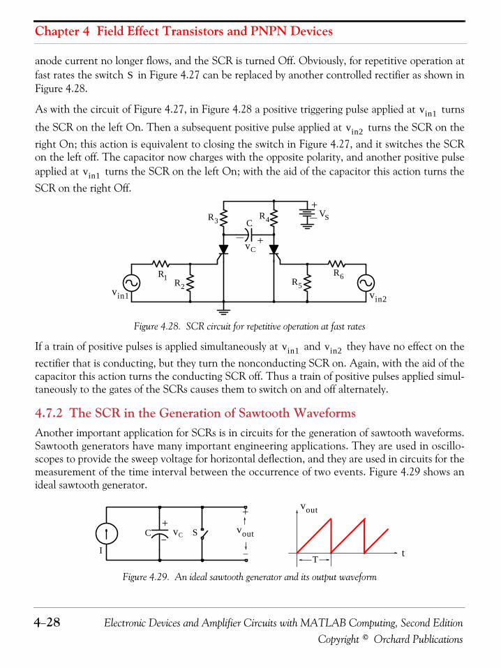
Chapter 4 Field Effect Transistors and PNPN Devices
4−28 Electronic Devices and Amplifier Circuits with MATLAB Computing, Second EditionCopyright © Orchard Publications
anode current no longer flows, and the SCR is turned Off. Obviously, for repetitive operation atfast rates the switch in Figure 4.27 can be replaced by another controlled rectifier as shown inFigure 4.28.
As with the circuit of Figure 4.27, in Figure 4.28 a positive triggering pulse applied at turns
the SCR on the left On. Then a subsequent positive pulse applied at turns the SCR on theright On; this action is equivalent to closing the switch in Figure 4.27, and it switches the SCRon the left off. The capacitor now charges with the opposite polarity, and another positive pulseapplied at turns the SCR on the left On; with the aid of the capacitor this action turns theSCR on the right Off.
Figure 4.28. SCR circuit for repetitive operation at fast rates
If a train of positive pulses is applied simultaneously at and they have no effect on therectifier that is conducting, but they turn the nonconducting SCR on. Again, with the aid of thecapacitor this action turns the conducting SCR off. Thus a train of positive pulses applied simul-taneously to the gates of the SCRs causes them to switch on and off alternately.
4.7.2 The SCR in the Generation of Sawtooth WaveformsAnother important application for SCRs is in circuits for the generation of sawtooth waveforms.Sawtooth generators have many important engineering applications. They are used in oscillo-scopes to provide the sweep voltage for horizontal deflection, and they are used in circuits for themeasurement of the time interval between the occurrence of two events. Figure 4.29 shows anideal sawtooth generator.
Figure 4.29. An ideal sawtooth generator and its output waveform
S
vin1
vin2
vin1
VS
R1
vin1
vC
R2
R3 R4
vin2
R6R5
C
+
+
vin1 vin2
+vC vout
vout
t
S
T
+
I
C
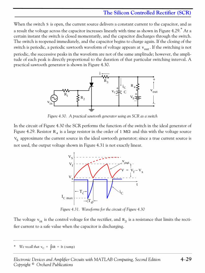
Electronic Devices and Amplifier Circuits with MATLAB Computing, Second Edition 4−29Copyright © Orchard Publications
The Silicon Controlled Rectifier (SCR)
When the switch is open, the current source delivers a constant current to the capacitor, and asa result the voltage across the capacitor increases linearly with time as shown in Figure 4.29.* At acertain instant the switch is closed momentarily, and the capacitor discharges through the switch.The switch is reopened immediately, and the capacitor begins to charge again. If the closing of theswitch is periodic, a periodic sawtooth waveform of voltage appears at . If the switching is notperiodic, the successive peaks in the waveform are not of the same amplitude; however, the ampli-tude of each peak is directly proportional to the duration of that particular switching interval. Apractical sawtooth generator is shown in Figure 4.30.
Figure 4.30. A practical sawtooth generator using an SCR as a switch
In the circuit of Figure 4.30 the SCR performs the function of the switch in the ideal generator ofFigure 4.29. Resistor is a large resistor in the order of and this with the voltage source
approximate the current source in the ideal sawtooth generator; since a true current source isnot used, the output voltage shown in Figure 4.31 is not exactly linear.
Figure 4.31. Waveforms for the circuit of Figure 4.30
The voltage is the control voltage for the rectifier, and is a resistance that limits the recti-fier current to a safe value when the capacitor is discharging.
* We recall that
S
vC I td∫ It ramp( )= =
vout
VSR1
vin
R2
R3R 4
+vC
voutiC
i
+
+
C
R 4 1 MΩ
VS
V Vf Vx–=
Vf
Vx
VS
Tc
Td
vout
iC
t
IC max
vin R3

Chapter 4 Field Effect Transistors and PNPN Devices
4−30 Electronic Devices and Amplifier Circuits with MATLAB Computing, Second EditionCopyright © Orchard Publications
When the SCR is switched off, the capacitor charges with a current from the DC supply voltage that is almost constant, and the capacitor voltage rises exponentially with time. The wave-
forms of voltage and current are shown in Figure 4.31. When the capacitor voltage reaches thecritical value , known as firing voltage, the SCR fires and discharges the capacitor rapidly.
When the capacitor is discharged to the critical voltage , referred to as the extinction voltage,the SCR switches off, and the cycle repeats itself.
The duration of the charging interval is determined by the firing voltage , the extinction
voltage , the capacitor current , and the capacitance . Since the firing voltage depends on
the control voltage , the amplitude and frequency, of the sawtooth wave can be adjusted by
adjusting . For a practical circuit triggering pulses of voltage can be applied at to controlthe firing of the SCR and thereby synchronize the sawtooth with an external signal.
The duration of the discharging interval depends on the amplitude of the sawtooth voltage,
the discharging current, and the capacitance . For rapid discharging, which is highly desired,the discharging current should be as large as possible; however, the current must be limited to avalue that is safe for the SCR. Thus, for good performance the SCR should have a high currentrating and short switching times.
All applications for the sawtooth generator require a highly linear sawtooth waveform and a shortdischarge time. These two quantities can be related in a very simple way to the important param-eters of the circuit. During the charging interval , the SCR is switched off, and the circuit is a
simple series connection of , , and . Thus, choosing at the beginning of the charg-ing interval, the equation for the output voltage during that interval has the form
* (4.21)
When , has its minimum value as shown in Figure 4.31; hence letting in(4.21) we obtain
or
and by substitution into (4.21)
(4.22)
* For an introduction to transient analysis, refer to Circuit Analysis I with MATLAB Applications, ISBN 978−0−9709511−2−0.
VS
Vf
Vx
Tc Vf
Vx iC C
vin
vin vin
Td
C
Tc
R 4 C VS t 0=
vout
vout VS Ae t R4C⁄–( )+=
t 0= vout Vx t 0=
vout VS A+ Vx= =
A Vx VS–=
vout VS VS Vx–( )e t R4C⁄–( )–=
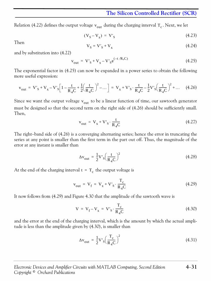
Electronic Devices and Amplifier Circuits with MATLAB Computing, Second Edition 4−31Copyright © Orchard Publications
The Silicon Controlled Rectifier (SCR)
Relation (4.22) defines the output voltage during the charging interval . Next, we let
(4.23)Then
(4.24)and by substitution into (4.22)
(4.25)
The exponential factor in (4.25) can now be expanded in a power series to obtain the followingmore useful expression:
(4.26)
Since we want the output voltage to be a linear function of time, our sawtooth generatormust be designed so that the second term on the right side of (4.26) should be sufficiently small.Then,
(4.27)
The right−band side of (4.26) is a converging alternating series; hence the error in truncating theseries at any point is smaller than the first term in the part out off. Thus, the magnitude of theerror at any instant is smaller than
(4.28)
At the end of the charging interval the output voltage is
(4.29)
It now follows from (4.29) and Figure 4.30 that the amplitude of the sawtooth wave is
(4.30)
and the error at the end of the charging interval, which is the amount by which the actual ampli-tude is less than the amplitude given by (4.30), is smaller than
(4.31)
vout Tc
VS Vx–( ) V'S=
VS V'S= Vx+
vout V'S Vx V'Se t R4C⁄–( )–+=
vout V'S Vx V'S 1 tR 4C----------- 1
2--- t
R 4C-----------⎝ ⎠
⎛ ⎞ 2…–+––+ Vx V'S
tR 4C-----------⋅ 1
2---V'S
tR 4C-----------⎝ ⎠
⎛ ⎞ 2– …+ += =
vout
vout Vx V'St
R 4C-----------⋅+=
Δvout12---V'S
tR 4C-----------⎝ ⎠
⎛ ⎞ 2=
t Tc=
vout Vf Vx V'STc
R 4C-----------⋅+= =
V Vf Vx– V'STc
R 4C-----------⋅= =
Δvout12---V'S
TcR 4C-----------⎝ ⎠
⎛ ⎞2
=

Chapter 4 Field Effect Transistors and PNPN Devices
4−32 Electronic Devices and Amplifier Circuits with MATLAB Computing, Second EditionCopyright © Orchard Publications
Solving (4.30) for and substituting the result into (4.31) we obtain
(4.32)
From (4.30) and (4.32)(4.33)
Relation (4.33) reveals that the fractional error depends only on the relative sizes of the sawtoothamplitude and the effective DC supply voltage; in order to have good linearity it is necessary tohave an effective supply voltage much larger than the required amplitude of the sawtooth. Goodlinearity is often obtained by the direct expedient of using a large supply voltage or by generatinga sawtooth wave of small amplitude. In more sophisticated designs the effect of a very large sup-ply voltage, often thousands of volts, is simulated by the use of additional circuitry in whichamplifiers are frequently used. One method of simulating a large supply voltage is illustrated inExample 4.5 at the end of this section. When the capacitor is charged from an ideal currentsource, as in Figure 4.28, the effective supply voltage is the open−circuit voltage of the source;this voltage is infinite, giving zero error.
In designing a sawtooth generator, and must be chosen so that the fractional error givenby (4.33) is sufficiently small. The time constant can then be chosen to produce the desiredslope to the sawtooth. With the control voltage in Figure 4.29 held constant, the firing volt-
age and the sawtooth amplitude are also constant, and the slope of the sawtooth deter-mines the length of the charging period. From Equation (4.30),
(4.34)
and when a train of triggering pulses is applied at , is determined by the interval between
the pulses, and the slope of the sawtooth determines the amplitude . With a fixed slope, is ameasure of the time interval .
At the end of the charging interval the SCR switches on, and the capacitor discharges exponen-tially through the SCR at a rate determined by the resistance in Figure 4.29. During the dis-charging interval the voltage across the capacitor changes by the amount
(4.35)
The duration of the discharging interval can be determined from this relation. To simplify the
Tc R 4C( )⁄
Δvout12--- V 2
V'S--------=
ΔvoutV
-------------- V2V'S-----------
Tc2R 4C--------------= =
VS V'SR 4C
vin
Vf V
Tc R 4C VV'S--------=
vin Tc
V VTc
R3
V Vf Vx–Qf Qx–
C------------------= =
Td

Electronic Devices and Amplifier Circuits with MATLAB Computing, Second Edition 4−33Copyright © Orchard Publications
The Silicon Controlled Rectifier (SCR)
calculation we will approximate the discharging current pulse, shown in Figure 4.30, with a pulsethat decreases linearly with time from the peak value to zero. With this approximation the
average value of the current during the discharging interval is , and the charge removed
from the capacitor during this interval is . Thus (4.33) can be written as
(4.36)
Also, since the capacitor current is approximately equal to the current through theSCR, we can express (4.36) as
(4.37)
or(4.38)
Division of (4.38) by (4.34) yields(4.39)
For good linearity we must have , and since the voltage drop across during the charg-
ing interval is approximately , and is very nearly the charging current for thecapacitor, (4.37) can be expressed as
(4.40)
where is the charging current for the capacitor, and is the peak discharging currentthrough the SCR. To provide a relatively short discharge time, the peak SCR current must bemuch greater than the capacitor charging current.
Any load that is connected across the output terminals of the sawtooth generator in Figure 4.30will affect the operation of the circuit, and any leakage resistance that develops across the capaci-tor has a similar effect. Figure 4.32(a) shows a sawtooth generator with a load resistor con-nected across the output terminals.
IC max
IC max 2⁄
Td IC max 2⁄
VTd IC max
2C-----------------------≈
IC max Imax
VTd Imax
2C-------------------≈
Td2CVImax------------=
TdTc------
2V'SR 4 Imax-------------------=
V V'S« R 4
V'S V'S R 4⁄ IC
TdTc------
2ICImax------------=
IC Imax
RL

Chapter 4 Field Effect Transistors and PNPN Devices
4−34 Electronic Devices and Amplifier Circuits with MATLAB Computing, Second EditionCopyright © Orchard Publications
Figure 4.32. A sawtooth generator with resistive load and its Thevenin equivalent
To simplify the circuit of Figure 4.32(a), we apply Thevenin’s theorem at points and weobtain the circuit of Figure 4.32(b) where
(4.41)
and
(4.42)
It is then evident that the addition of the load resistor affects both the slope and the linearityof the sawtooth waveform. The presence of affects the effective DC supply voltage, andhence on the linearity, is especially severe. Therefore, it becomes necessary to make greater
than . A load resistor of about would reduce the effective supply voltage and willincrease the fractional error by a factor of more than . It is quite possible in such cases for theeffective voltage to be less than the firing voltage , for the SCR; then the rectifier neverfires, and no sawtooth wave is generated. Accordingly, the output from the sawtooth generatormust be connected to a very high impedance device such as a MOSFET. The output can also bedelivered to a bipolar junction transistor, but a very special circuit configuration must be used toprovide the required high input resistance.
VTH
R3RTH+ vC
iC
i
SCRCircuit
VS
R3R 4+
vC
iC
i
SCRCircuit
RL vout
a( )
b( )
y
x
+
+C
+
+
C
x y–
VTHRL
R 4 RL+------------------- VS⋅=
RTHR 4RL
R 4 RL+-------------------=
RL
RL
RL
1 MΩ 100 KΩ10
VTH Vf
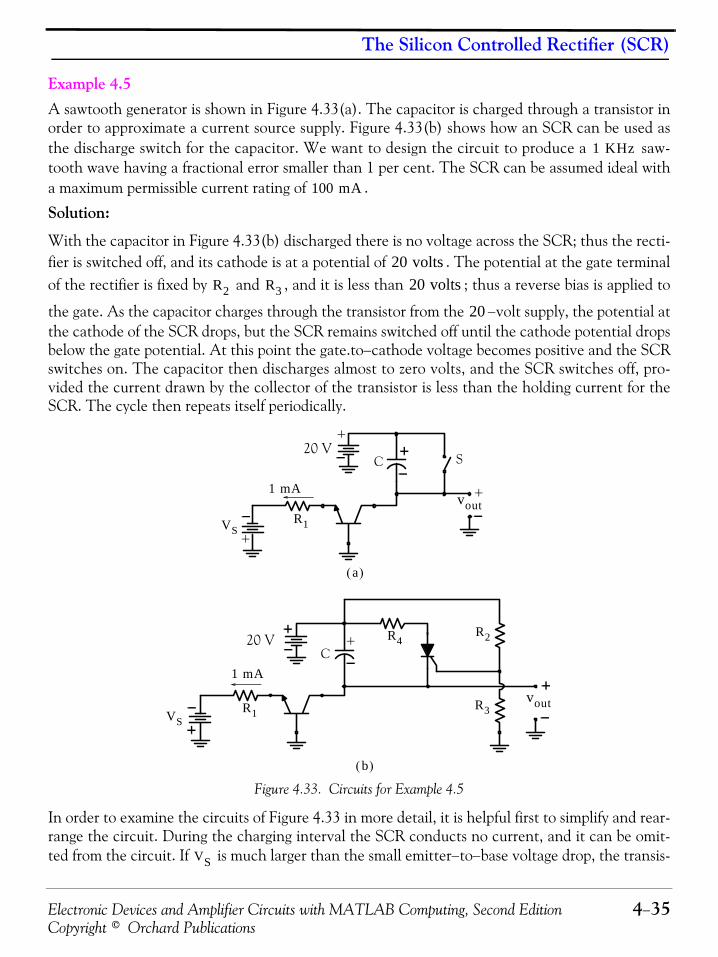
Electronic Devices and Amplifier Circuits with MATLAB Computing, Second Edition 4−35Copyright © Orchard Publications
The Silicon Controlled Rectifier (SCR)
Example 4.5 A sawtooth generator is shown in Figure 4.33(a). The capacitor is charged through a transistor inorder to approximate a current source supply. Figure 4.33(b) shows how an SCR can be used asthe discharge switch for the capacitor. We want to design the circuit to produce a saw-tooth wave having a fractional error smaller than 1 per cent. The SCR can be assumed ideal witha maximum permissible current rating of .
Solution:
With the capacitor in Figure 4.33(b) discharged there is no voltage across the SCR; thus the recti-fier is switched off, and its cathode is at a potential of . The potential at the gate terminalof the rectifier is fixed by and , and it is less than ; thus a reverse bias is applied to
the gate. As the capacitor charges through the transistor from the −volt supply, the potential atthe cathode of the SCR drops, but the SCR remains switched off until the cathode potential dropsbelow the gate potential. At this point the gate.to−cathode voltage becomes positive and the SCRswitches on. The capacitor then discharges almost to zero volts, and the SCR switches off, pro-vided the current drawn by the collector of the transistor is less than the holding current for theSCR. The cycle then repeats itself periodically.
Figure 4.33. Circuits for Example 4.5
In order to examine the circuits of Figure 4.33 in more detail, it is helpful first to simplify and rear-range the circuit. During the charging interval the SCR conducts no current, and it can be omit-ted from the circuit. If is much larger than the small emitter−to−base voltage drop, the transis-
1 KHz
100 mA
20 voltsR2 R3 20 volts
20
C S20 V
VSR1
1 mA
20 V
VSR1
1 mA
R3
R2R4
vout
a( )
b( )
vout
C
VS
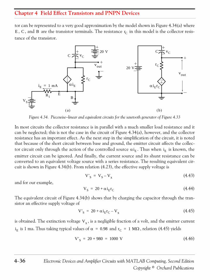
Chapter 4 Field Effect Transistors and PNPN Devices
4−36 Electronic Devices and Amplifier Circuits with MATLAB Computing, Second EditionCopyright © Orchard Publications
tor can be represented to a very good approximation by the model shown in Figure 4.34(a) where, , and are the transistor terminals. The resistance in this model is the collector resis-
tance of the transistor.
Figure 4.34. Piecewise−linear and equivalent circuits for the sawtooth generator of Figure 4.33
In most circuits the collector resistance is in parallel with a much smaller load resistance and itcan be neglected; this is not the case in the circuit of Figure 4.34(a), however, and the collectorresistance has an important effect. As the next step in the simplification of the circuit, it is notedthat because of the short circuit between base and ground, the emitter circuit affects the collec-tor circuit only through the action of the controlled source . Thus when is known, theemitter circuit can be ignored. And finally, the current source and its shunt resistance can beconverted to an equivalent voltage source with a series resistance. The resulting equivalent cir-cuit is shown in Figure 4.34(b). From relation (4.23), the effective supply voltage is
(4.43)and for our example,
(4.44)
The equivalent circuit of Figure 4.34(b) shows that by charging the capacitor through the tran-sistor an effective supply voltage of
(4.45)
is obtained. The extinction voltage , is a negligible fraction of a volt, and the emitter current
is 1 ma. Thus taking typical values of and , relation (4.45) yields
(4.46)
E C B rC
VS
R1
a( ) b( )
αiE
20 V
iE 1 mA=
E
C
B
vout
C
αiErC
rC
vout
20 VrC
vC
vC
αiE iE
V'S VS Vx–=
VS 20 αiErC+=
V'S 20 αiErC Vx–+=
Vx
iE α 0.98= rC 1 MΩ=
V'S 20 980+ 1000 V= =

Electronic Devices and Amplifier Circuits with MATLAB Computing, Second Edition 4−37Copyright © Orchard Publications
The Silicon Controlled Rectifier (SCR)
For a fractional error of 1 per cent in the amplitude of the sawtooth, relation (4.33) yields
(4.47)
and thus(4.48)
Thus, in principle the amplitude of the sawtooth output can be as large as the DC supply voltage;however, to avoid possible non linearities in the transistor characteristics at low voltages and toallow for possible variations in the supply voltage, a value of 15 volts might be chosen for .Accordingly, the values of resistors and should be chosen to make the gate−terminal poten-tial about 5 volts when the SCR is switched off.
To limit the SCR current to the maximum safe value of 100 ma, the value of resistor should be
(4.49)
For a sawtooth frequency of ,
(4.50)
From (4.40)(4.51)
With , and using (4.50) and (4.51) we obtain
(4.52)
and thus(4.53)
Finally, from (4.34)
or(4.54)
where is as shown in Figure 4.34(b).
ΔvoutV
-------------- 0.01 V2V'S-----------= =
V 20 V=
VR2 R3
R4
R4V
Imax----------- 15
0.1------- 150 Ω= = =
1 KHz
Tc Td+ Tc 1TdTc------+
⎝ ⎠⎜ ⎟⎛ ⎞ 1
f--- 0.001 sec= = =
TdTc------
2ICImax------------=
IC αiE≈ 1 mA= Imax 100 mA=
Tc 1 2 1100---------+⎝ ⎠
⎛ ⎞ 1.02Tc 0.001= =
Tc 0.00098 sec=
Tc R4C VV'S--------=
CTcR4------
V'SV
-------- 0.00098
106------------------- 1000
15------------⋅ 0.0655 μF= = =
R4 rC 1 MΩ= =
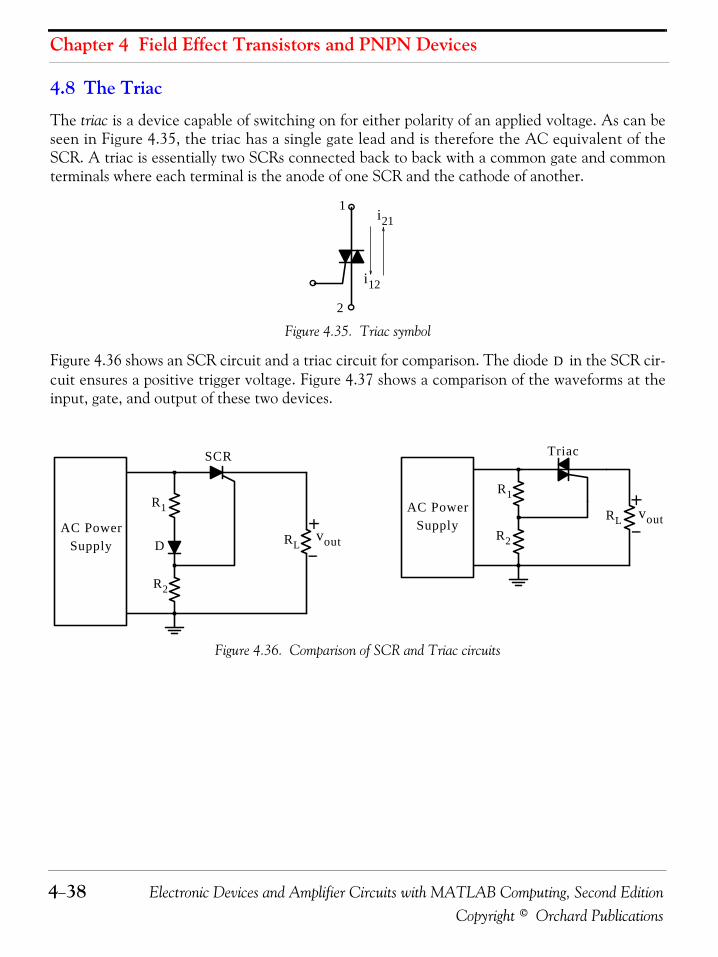
Chapter 4 Field Effect Transistors and PNPN Devices
4−38 Electronic Devices and Amplifier Circuits with MATLAB Computing, Second EditionCopyright © Orchard Publications
4.8 The Triac
The triac is a device capable of switching on for either polarity of an applied voltage. As can beseen in Figure 4.35, the triac has a single gate lead and is therefore the AC equivalent of theSCR. A triac is essentially two SCRs connected back to back with a common gate and commonterminals where each terminal is the anode of one SCR and the cathode of another.
Figure 4.35. Triac symbol
Figure 4.36 shows an SCR circuit and a triac circuit for comparison. The diode in the SCR cir-cuit ensures a positive trigger voltage. Figure 4.37 shows a comparison of the waveforms at theinput, gate, and output of these two devices.
Figure 4.36. Comparison of SCR and Triac circuits
2
1
i12
i21
D
SCR
D
AC PowerSupply
Triac
RLvout
RL voutR1
R2
R1
R2AC Power
Supply
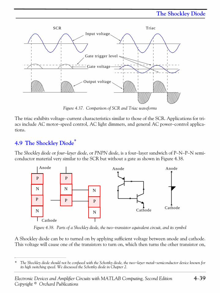
Electronic Devices and Amplifier Circuits with MATLAB Computing, Second Edition 4−39Copyright © Orchard Publications
The Shockley Diode
Figure 4.37. Comparison of SCR and Triac waveforms
The triac exhibits voltage−current characteristics similar to those of the SCR. Applications for tri-acs include AC motor−speed control, AC light dimmers, and general AC power−control applica-tions.
4.9 The Shockley Diode*
The Shockley diode or four−layer diode, or PNPN diode, is a four−layer sandwich of P−N−P−N semi-conductor material very similar to the SCR but without a gate as shown in Figure 4.38.
Figure 4.38. Parts of a Shockley diode, the two−transistor equivalent circuit, and its symbol
A Shockley diode can be to turned on by applying sufficient voltage between anode and cathode.This voltage will cause one of the transistors to turn on, which then turns the other transistor on,
* The Shockley diode should not be confused with the Schottky diode, the two−layer metal−semiconductor device known forits high switching speed. We discussed the Schottky diode in Chapter 2.
Input voltageSCR Triac
Output voltage
Gate voltage
Gate trigger level
P
P
N
N
P
P
N
P
N
N
Anode
Cathode
Anode
Cathode
Anode
Cathode
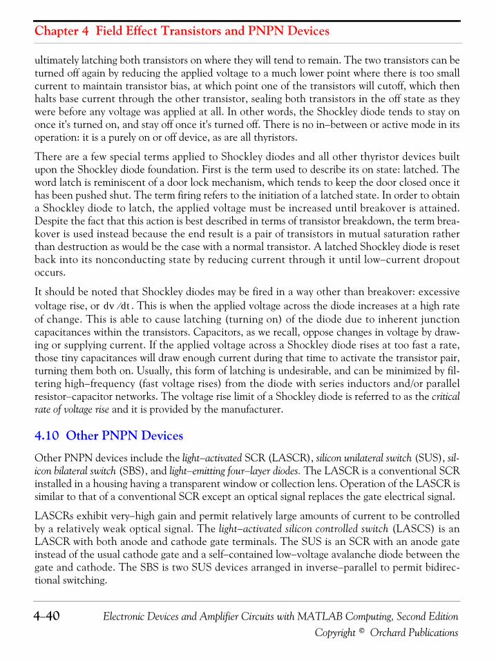
Chapter 4 Field Effect Transistors and PNPN Devices
4−40 Electronic Devices and Amplifier Circuits with MATLAB Computing, Second EditionCopyright © Orchard Publications
ultimately latching both transistors on where they will tend to remain. The two transistors can beturned off again by reducing the applied voltage to a much lower point where there is too smallcurrent to maintain transistor bias, at which point one of the transistors will cutoff, which thenhalts base current through the other transistor, sealing both transistors in the off state as theywere before any voltage was applied at all. In other words, the Shockley diode tends to stay ononce it's turned on, and stay off once it's turned off. There is no in−between or active mode in itsoperation: it is a purely on or off device, as are all thyristors.
There are a few special terms applied to Shockley diodes and all other thyristor devices builtupon the Shockley diode foundation. First is the term used to describe its on state: latched. Theword latch is reminiscent of a door lock mechanism, which tends to keep the door closed once ithas been pushed shut. The term firing refers to the initiation of a latched state. In order to obtaina Shockley diode to latch, the applied voltage must be increased until breakover is attained.Despite the fact that this action is best described in terms of transistor breakdown, the term brea-kover is used instead because the end result is a pair of transistors in mutual saturation ratherthan destruction as would be the case with a normal transistor. A latched Shockley diode is resetback into its nonconducting state by reducing current through it until low−current dropoutoccurs.
It should be noted that Shockley diodes may be fired in a way other than breakover: excessivevoltage rise, or . This is when the applied voltage across the diode increases at a high rateof change. This is able to cause latching (turning on) of the diode due to inherent junctioncapacitances within the transistors. Capacitors, as we recall, oppose changes in voltage by draw-ing or supplying current. If the applied voltage across a Shockley diode rises at too fast a rate,those tiny capacitances will draw enough current during that time to activate the transistor pair,turning them both on. Usually, this form of latching is undesirable, and can be minimized by fil-tering high−frequency (fast voltage rises) from the diode with series inductors and/or parallelresistor−capacitor networks. The voltage rise limit of a Shockley diode is referred to as the criticalrate of voltage rise and it is provided by the manufacturer.
4.10 Other PNPN Devices
Other PNPN devices include the light−activated SCR (LASCR), silicon unilateral switch (SUS), sil-icon bilateral switch (SBS), and light−emitting four−layer diodes. The LASCR is a conventional SCRinstalled in a housing having a transparent window or collection lens. Operation of the LASCR issimilar to that of a conventional SCR except an optical signal replaces the gate electrical signal.
LASCRs exhibit very−high gain and permit relatively large amounts of current to be controlledby a relatively weak optical signal. The light−activated silicon controlled switch (LASCS) is anLASCR with both anode and cathode gate terminals. The SUS is an SCR with an anode gateinstead of the usual cathode gate and a self−contained low−voltage avalanche diode between thegate and cathode. The SBS is two SUS devices arranged in inverse−parallel to permit bidirec-tional switching.
dv dt⁄
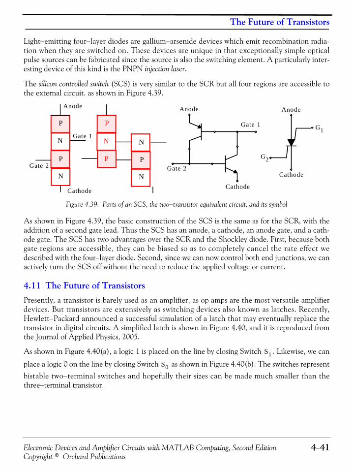
Electronic Devices and Amplifier Circuits with MATLAB Computing, Second Edition 4−41Copyright © Orchard Publications
The Future of Transistors
Light−emitting four−layer diodes are gallium−arsenide devices which emit recombination radia-tion when they are switched on. These devices are unique in that exceptionally simple opticalpulse sources can be fabricated since the source is also the switching element. A particularly inter-esting device of this kind is the PNPN injection laser.
The silicon controlled switch (SCS) is very similar to the SCR but all four regions are accessible tothe external circuit. as shown in Figure 4.39.
Figure 4.39. Parts of an SCS, the two−transistor equivalent circuit, and its symbol
As shown in Figure 4.39, the basic construction of the SCS is the same as for the SCR, with theaddition of a second gate lead. Thus the SCS has an anode, a cathode, an anode gate, and a cath-ode gate. The SCS has two advantages over the SCR and the Shockley diode. First, because bothgate regions are accessible, they can be biased so as to completely cancel the rate effect wedescribed with the four−layer diode. Second, since we can now control both end junctions, we canactively turn the SCS off without the need to reduce the applied voltage or current.
4.11 The Future of TransistorsPresently, a transistor is barely used as an amplifier, as op amps are the most versatile amplifierdevices. But transistors are extensively as switching devices also known as latches. Recently,Hewlett−Packard announced a successful simulation of a latch that may eventually replace thetransistor in digital circuits. A simplified latch is shown in Figure 4.40, and it is reproduced fromthe Journal of Applied Physics, 2005.
As shown in Figure 4.40(a), a logic 1 is placed on the line by closing Switch . Likewise, we can
place a logic 0 on the line by closing Switch as shown in Figure 4.40(b). The switches representbistable two−terminal switches and hopefully their sizes can be made much smaller than thethree−terminal transistor.
P
P
N
N
P
P
N
P
N
N
Anode
Cathode
Gate 2
Anode
Cathode
Gate 1
Anode
Cathode
G2
G1
Gate 2
Gate 1
S1
S0
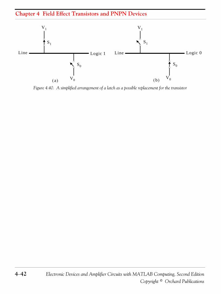
Chapter 4 Field Effect Transistors and PNPN Devices
4−42 Electronic Devices and Amplifier Circuits with MATLAB Computing, Second EditionCopyright © Orchard Publications
Figure 4.40. A simplified arrangement of a latch as a possible replacement for the transistor
Line Line
V1 V1
V0 V0
Logic 1 Logic 0
S1 S1
S0 S0
a( ) b( )
Electronic Devices and Amplifier Circuits with MATLAB Computing, Second Edition 4−43Copyright © Orchard Publications
Summary
4.12 Summary• The Field−Effect Transistor (FET) is another semiconductor device. The FET is a voltage−
controlled device.The Junction FET (JFET) is the earlier type and the Metal Oxide Semicon-ductor FET (MOSFET) is now the most popular type. A FET has four terminals, drain,source, gate and substrate. The substrate is normally connected to the source and thus a FET isessentially a three−terminal device.
• One of the most attractive features of the FET is the fact that the input resistance, measuredbetween gate and source, can be made very large, from 1 to 100 megohms.
• N−channel FETs are the most common. P−channel FETs operate similarly except that thevoltage polarities are reversed.
• One important parameter in FETs is its transconductance defined as the ratio of the
change in current to the change of voltage which produced it. In other words,
In other words, the transconductance is a measure of the sensitivity of drain current to changesin gate−to−source bias.
• A MOSFET is said to operate in the depletion mode when a negative voltage is applied at thegate. The JFET also operates in this manner. A MOSFET is said to operate in the enhance-ment mode if a positive voltage is applied at the gate. A MOSFET can be constructed that willoperate in either mode depending upon what type of bias is applied, thus allowing a greaterrange of input signals.
• In a MOSFET, the voltage at which the channel is closed is known as the pinch−off voltage, and the minimum voltage required to form a conducting channel between the drain and
source is referred to as the threshold voltage and it is denoted as . Typical values for are2 to 4 volts for high voltage devices with thicker gate oxides, and 1 to 2 volts for lower voltagedevices with thinner gate oxides.
• In a MOSFET, the three regions of operation are the cutoff, the quadratic or triode, and thesaturation or pentode. In the cutoff mode, and no drain current flows. In the qua-dratic region the drain current is determined from the expression
and in the saturation region from the expression
gm
iDS vGS
gm∂iDS∂vGS------------
vDS cons ttan=
=
VP
VT VT
vGS VT<
iD knWL----- vGS VT–( )vDS
12---vDS
2–= for vDS vGS VT–≤
Chapter 4 Field Effect Transistors and PNPN Devices
4−44 Electronic Devices and Amplifier Circuits with MATLAB Computing, Second EditionCopyright © Orchard Publications
where is a constant depending on electron mobility, and oxide thickness, permittivity, andcapacitance for n−channel MOSFETs. For p−channel MOSFETs this parameter is denoted as
. The ratio denotes the ratio of the channel width to channel length . Typical
values of are around , for , around , and for about .
• For small signals, transconductance is defined as
• The output conductance is defined as
• The voltage gain in a MOSFET device is defined as
and the minus (−) sign indicates phase reversal.
• In high density integrated circuits, current mirrors are normally used in lieu of resistors.
• Complementary MOS or CMOS technology combines one NMOS device and one PMOSdevice into a single device referred to as CMOS. These devices are used extensively in bothanalog and digital circuits, and integrated circuits. Also, CMOS devices are the most commonamplifiers in the FET technology.
• In CMOS devices only one of its components is on at any given time, that is, either theNMOS device is on and the PMOS device is off, or vice versa. Thus, CMOS chips require lesspower than chips using just one type of a MOSFET, and unlike bipolar transistors, a CMOShas almost no static power dissipation.
• A CMOS device can be configured as a common−source amplifier, common−gate amplifier,and common−drain or source follower.
• The Metal−Semiconductor−Field−Effect−Transistor (MESFET) consists of a conductingchannel positioned between a source and drain contact region. The carrier flow from sourceto drain is controlled by a Schottky metal gate. The control of the channel is obtained byvarying the depletion layer width underneath the metal contact which modulates the thick-
iD12--- kn
WL-----⋅ vGS VT–( )2
= for vDS vGS VT–≥
kn
kp W L⁄ W L
kn 20 μA V2⁄ kp 10 μA V2⁄ W L⁄ 10
gmid
vgs------- kn
WL----- VGS VT–( )= =
go∂iD
∂vDS------------
vGS cons ttan=
=
Av
Avvdvgs------- RDgm–= =
180°
Electronic Devices and Amplifier Circuits with MATLAB Computing, Second Edition 4−45Copyright © Orchard Publications
Summary
ness of the conducting channel and thereby the current MESFETs use GaAs (gallium ars-enide) technology. Only MESFETS are available because holes have a slowermobility.
• The unijunction transistor (UJT) is a three−terminal, single−junction device which exhibitsnegative resistance and switching characteristics totally unlike those of conventional bipolartransistors. UJTs can be used for the design of pulse and sawtooth generators, analog−to−digi-tal converters, relay time delay circuits, and frequency dividers. Other UJT devices, referred toas programmable UJTs, can have their parameters set by external components such as resistorsand capacitors.
• The diac is a two−terminal, transistor−like component which exhibits bistable switching foreither polarity of a suitably high applied voltage. The diac closely resembles a PNP transistorwithout an external base terminal. Its major application is in conjunction with a triac to pro-duce AC phase−control circuits useful for motor−speed control, light dimming, and other acpower−control functions.
• The silicon controlled rectifier (SCR) is a four−layer semiconducting device, with each layerconsisting of an alternately N or P−type material, for example N−P−N−P. The main terminals,labelled anode and cathode, are across the full four layers, and the control terminal, called thegate, is attached to one of the middle layers. Another name for the SCR is thyristor. It is similarto a diode with an additional terminal that is used to turn it on. Once turned on, the SCR willremain on as long as current flows through it. If the current falls to zero, the SCR behaves likean open switch.
• The triac is a device capable of switching on for either polarity of an applied voltage; It is theAC equivalent of the SCR.
• The Shockley diode, (not to be confused with the Schottky diode), or four−layer diode, orPNPN diode, is a four−layer sandwich of P−N−P−N semiconductor material very similar to theSCR but without a gate.
• The silicon controlled switch (SCS) is very similar to the SCR but all four regions are accessi-ble to the external circuit.
n channel–

Chapter 4 Field Effect Transistors and PNPN Devices
4−46 Electronic Devices and Amplifier Circuits with MATLAB Computing, Second EditionCopyright © Orchard Publications
4.13 Exercises1. For the JFET amplifier circuit below, prove that the voltage gain depends only on the
transconductance and the value of the drain resistor , that is, show that .
2. Compute the value of for an NMOS device where , ,, , and .
3. Draw an equivalent circuit that represents the MOSFET in the saturation mode.
4. An MOSFET with , , , and , is
biased with and .
a. Compute the drain current
b. Compute the transconductance
c. Compute the output conductance if
d. Compute the output conductance if
5. An enhancement−type MOSFET with , ,
, and , is biased with and . What is the highestvoltage of that will keep the device in saturation?
6. In the circuit below, the SCR is used to control the power delivered to the load by thesinusoidal source. As shown, the gate supply is adjustable.
a. Over what range may the conduction angle of the SCR be continuously varied?
b. Over what range may the load DC current be continuously varied if the frequency is?
AV
gm RD AV gmRD–=
D
S
G
VDD
vin
vout+
+
+
rDS k 18 μA V2⁄= L 5 μm=
W 60 μm= VT 2 V= vGS 4 V=
n channel–
n channel– kn 50 10 6–×= W 10 μm= L 1 μm= VT 1 V=
vGS 3 V= vDS 5 V=
iD
gm
go VDS 2 V=
go VDS 0 V=
p channel– kp 10 10 6–×= W 10 μm=
L 1 μm= VT 2– V= vG 0 V= vS 5 V=
vD
50 ΩVGG
60 Hz

Electronic Devices and Amplifier Circuits with MATLAB Computing, Second Edition 4−47Copyright © Orchard Publications
Exercises
7. The circuit below is in steady state with the switch open and the SCR is in the conductingstate. The voltage drop across the SCR is while it is conducting. The switch is then closedat , and it is assumed that the SCR switches instantly to the non−conducting state andremains non−conducting thereafter.
a. What are the initial and final values of the voltage across the capacitor with the polaritiesshown?
b. If the anode potential of the SCR must remain negative for to ensure that the SCRswitches to the non−conducting state, what is the minimum value of the capacitor thatshould be used?
VGG100 ωtsin
Rload
RG
50 Ω
1 Vt 0=
10 μsC
R3 R4
R1
R2
C
S
1 KΩ
50 KΩ
10 KΩ
20 KΩ
VDC 50 V
100 ωtsin
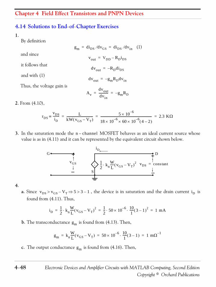
Chapter 4 Field Effect Transistors and PNPN Devices
4−48 Electronic Devices and Amplifier Circuits with MATLAB Computing, Second EditionCopyright © Orchard Publications
4.14 Solutions to End−of−Chapter Exercises1.
By definition (1)
and since
it follows that
and with (1)
Thus, the voltage gain is
2. From (4.10),
3. In the saturation mode the MOSFET behaves as an ideal current source whosevalue is as in (4.11) and it can be represented by the equivalent circuit shown below.
4.a. Since , the device is in saturation and the drain current is
found from (4.11). Thus,
b. The transconductance is found from (4.13). Then,
c. The output conductance is found from (4.16). Then,
gm diDS dvGS⁄ diDS dvin⁄= =
vout VDD RDiDS–=
dvout RDdiDS–=
dvout gmRDdvin–=
Avdvoutdvin------------- gmRD–= =
rDSvDSiD
---------≡ LkW vGS VT–( )------------------------------------ 5 10 6–×
18 10 6–× 60 10 6– 4 2–( )××---------------------------------------------------------------------- 2.3 KΩ= = =
n channel–
D
S
G
vGS vDS cons ttan=
iD
12--- kn
WL-----⋅ vGS VT–( )2
vDS vGS VT–> 5 3 1–>⇒ iD
iD12--- kn
WL-----⋅ vGS VT–( )2 1
2--- 50 10 6–× 10
1------⋅⋅ 3 1–( )2 1 mA= = =
gm
gm knWL----- vGS VT–( ) 50 10 6–× 10
1------⋅ 3 1–( ) 1 mΩ 1–
= = =
gm
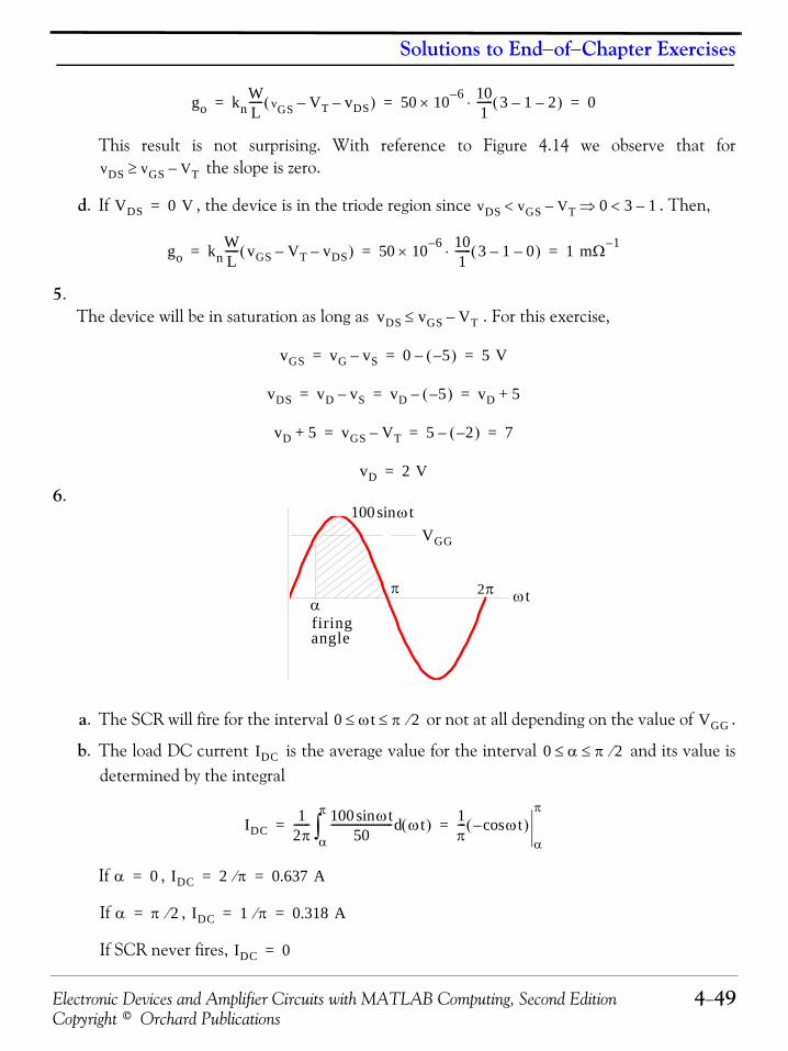
Electronic Devices and Amplifier Circuits with MATLAB Computing, Second Edition 4−49Copyright © Orchard Publications
Solutions to End−of−Chapter Exercises
This result is not surprising. With reference to Figure 4.14 we observe that for the slope is zero.
d. If , the device is in the triode region since . Then,
5.The device will be in saturation as long as . For this exercise,
6.
a. The SCR will fire for the interval or not at all depending on the value of .
b. The load DC current is the average value for the interval and its value isdetermined by the integral
If ,
If ,
If SCR never fires,
go knWL----- vGS VT– vDS–( ) 50 10 6–× 10
1------ 3 1– 2–( )⋅ 0= = =
vDS vGS VT–≥
VDS 0 V= vDS vGS VT–< 0 3 1–<⇒
go knWL----- vGS VT– vDS–( ) 50 10 6–× 10
1------ 3 1– 0–( )⋅ 1 mΩ 1–
= = =
vDS vGS VT–≤
vGS vG vS– 0 5–( )– 5 V= = =
vDS vD vS– vD 5–( )– vD 5+= = =
vD 5+ vGS VT– 5 2–( )– 7= = =
vD 2 V=
0 1 2 3 4 5 6 7-1
-0.5
0
0.5
1
απ 2π ωt
VGG
100 ωsin t
firingangle
0 ωt π 2⁄≤≤ VGG
IDC 0 α π 2⁄≤ ≤
IDC1
2π------ 100 ωtsin
50----------------------- ωt( )d
α
π
∫1π--- ωtcos–( )
α
π= =
α 0= IDC 2 π⁄ 0.637 A= =
α π 2⁄= IDC 1 π⁄ 0.318 A= =
IDC 0=

Chapter 4 Field Effect Transistors and PNPN Devices
4−50 Electronic Devices and Amplifier Circuits with MATLAB Computing, Second EditionCopyright © Orchard Publications
7.
a. Just before the switch closes, the voltage drop across the SCR is and the voltage dropacross the capacitor is with the polarity as shown. The capacitor voltage cannotchange instantaneously so immediately after the switch is closed, the capacitor voltage willbe as shown in the figure below, and the SCR will be Off.
The capacitor voltage will eventually charge to with respect to the ground and thusit will undergo a change from (initial value) to (final value).
b. We want the SCR anode to remain negative for , that is, until the voltage across thecapacitor reaches the value of . Using the general formula for the capacitor voltage, wemust have
or
R3 R4
R1
R2
C
S
1 KΩ50 KΩ
10 KΩ20 KΩ
VDC 50 V
100 ωtsin
1 V49 V
49– V
VDC50 V
R3 1 KΩR4 50 KΩ
C
50 V49– V +50 V
10 μs0 V
vC t( ) V∞ V∞ Vinitial–( )e t– RC( )⁄–=
0 50 50 49–( )–[ ]e t– RC( )⁄–=
e t– RC( )⁄ 50 99⁄=
t– R3C( )⁄ 50 99⁄( )ln=
Ct R3⁄–
50 99⁄( )ln-------------------------- 10 10 6–×–( ) 103⁄
0.683–-------------------------------------------- 14.64 nF= ==

Electronic Devices and Amplifier Circuits with MATLAB Computing, Second Edition 5−1Copyright © Orchard Publications
Chapter 5
Operational Amplifiers
his chapter begins with an introduction to operational amplifiers (op amps), characteristics,and applications. We will discuss the ideal op amp, analysis of circuits in the inverting andnon−inverting configurations, and gain and bandwidth on circuit performance. We will also
introduce some circuits consisting of op amps and non−linear devices, and analog computers.
5.1 The Operational AmplifierThe operational amplifier or simply op amp, is the most versatile electronic amplifier. It derives itname from the fact that it is capable of performing many mathematical operations such as addi-tion, multiplication, differentiation, integration, and analog−to−digital conversion or vice versa. Itcan also be used as a comparator and electronic filter. It is also the basic block in analog computerdesign. Its symbol and pinouts are shown in Figure 5.1.
Figure 5.1. Symbol and pinouts for operational amplifier
As shown above the op amp has two inputs but only one output. For this reason it is referred to asdifferential input, single ended output amplifier. Figure 5.2 shows the internal construction of thepopular 741 op amp. This figure also shows terminals and . These are the voltage sourcesrequired to power up the op amp. Typically, is +15 volts and is −15 volts. These terminalsare not shown in op amp circuits since they just provide power, and do not reveal any other usefulinformation for the op amp’s circuit analysis.
5.2 An Overview of the Op AmpThe op amp has the following important characteristics:
1. Very high input impedance (resistance)
2. Very low output impedance (resistance)
3. Capable of producing a very large gain that can be set to any value by connection of externalresistors of appropriate values
T
62
+
−7
34
V −
V +
V + V −
V + V −
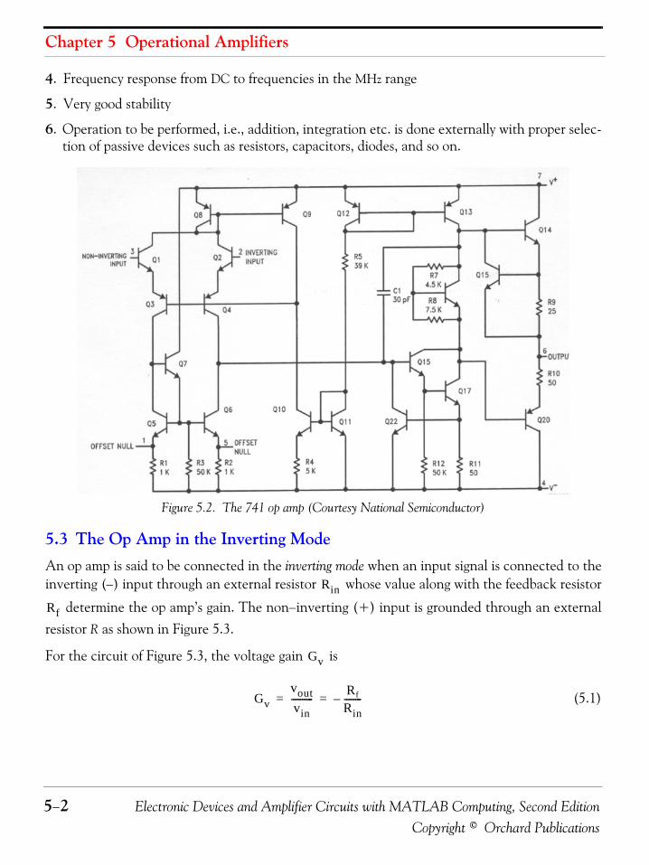
Chapter 5 Operational Amplifiers
5−2 Electronic Devices and Amplifier Circuits with MATLAB Computing, Second EditionCopyright © Orchard Publications
4. Frequency response from DC to frequencies in the MHz range
5. Very good stability
6. Operation to be performed, i.e., addition, integration etc. is done externally with proper selec-tion of passive devices such as resistors, capacitors, diodes, and so on.
Figure 5.2. The 741 op amp (Courtesy National Semiconductor)
5.3 The Op Amp in the Inverting ModeAn op amp is said to be connected in the inverting mode when an input signal is connected to theinverting (−) input through an external resistor whose value along with the feedback resistor
determine the op amp’s gain. The non−inverting (+) input is grounded through an externalresistor R as shown in Figure 5.3.
For the circuit of Figure 5.3, the voltage gain is
(5.1)
Rin
Rf
Gv
Gvvoutvin---------- Rf
Rin--------–= =
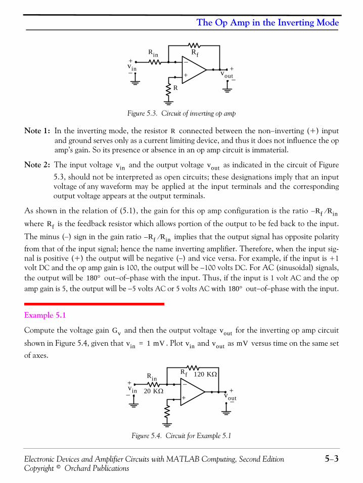
Electronic Devices and Amplifier Circuits with MATLAB Computing, Second Edition 5−3Copyright © Orchard Publications
The Op Amp in the Inverting Mode
Figure 5.3. Circuit of inverting op amp
Note 1: In the inverting mode, the resistor connected between the non−inverting (+) inputand ground serves only as a current limiting device, and thus it does not influence the opamp’s gain. So its presence or absence in an op amp circuit is immaterial.
Note 2: The input voltage and the output voltage as indicated in the circuit of Figure5.3, should not be interpreted as open circuits; these designations imply that an inputvoltage of any waveform may be applied at the input terminals and the correspondingoutput voltage appears at the output terminals.
As shown in the relation of (5.1), the gain for this op amp configuration is the ratio
where is the feedback resistor which allows portion of the output to be fed back to the input.
The minus (−) sign in the gain ratio implies that the output signal has opposite polarityfrom that of the input signal; hence the name inverting amplifier. Therefore, when the input sig-nal is positive (+) the output will be negative (−) and vice versa. For example, if the input is +1volt DC and the op amp gain is 100, the output will be −100 volts DC. For AC (sinusoidal) signals,the output will be out−of−phase with the input. Thus, if the input is 1 volt AC and the opamp gain is 5, the output will be −5 volts AC or 5 volts AC with out−of−phase with the input.
Example 5.1
Compute the voltage gain and then the output voltage for the inverting op amp circuit
shown in Figure 5.4, given that . Plot and as versus time on the same setof axes.
Figure 5.4. Circuit for Example 5.1
R
+
−
vin
Rf
vout
Rin
+
+ −−
R
vin vout
Rf Rin⁄–
Rf
Rf Rin⁄–
180°180°
Gv vout
vin 1 mV= vin vout mV
−+
RinRf
vin vout
120 KΩ
20 KΩ+
+−−
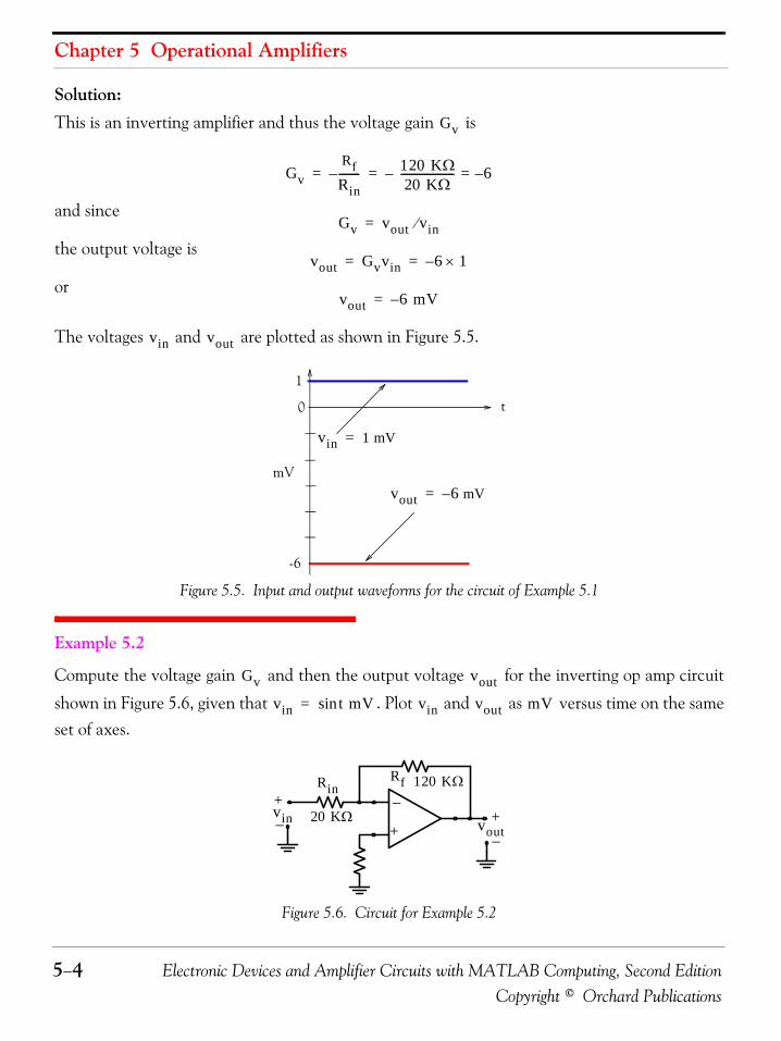
Chapter 5 Operational Amplifiers
5−4 Electronic Devices and Amplifier Circuits with MATLAB Computing, Second EditionCopyright © Orchard Publications
Solution:
This is an inverting amplifier and thus the voltage gain is
and since
the output voltage is
or
The voltages and are plotted as shown in Figure 5.5.
Figure 5.5. Input and output waveforms for the circuit of Example 5.1
Example 5.2
Compute the voltage gain and then the output voltage for the inverting op amp circuit
shown in Figure 5.6, given that . Plot and as versus time on the sameset of axes.
Figure 5.6. Circuit for Example 5.2
Gv
GvRfRin--------– 120 KΩ
20 KΩ-------------------- 6–=–= =
Gv vout vin⁄=
vout Gvvin 6 1×–= =
vout 6 mV–=
vin vout
0
-6
1
mV
t
vin 1 mV=
vout 6– mV=
Gv vout
vin t sin mV= vin vout mV
−+
RinRf
vin vout
120 KΩ
20 KΩ+
+−−
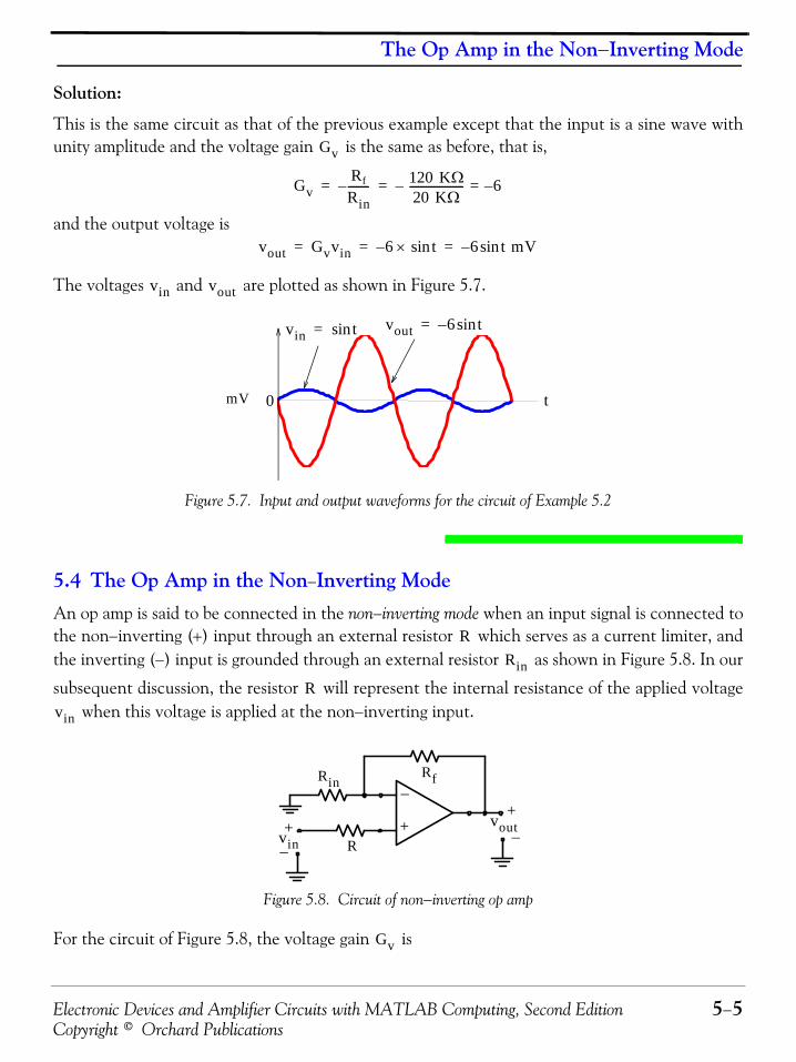
Electronic Devices and Amplifier Circuits with MATLAB Computing, Second Edition 5−5Copyright © Orchard Publications
The Op Amp in the Non−Inverting Mode
Solution:
This is the same circuit as that of the previous example except that the input is a sine wave withunity amplitude and the voltage gain is the same as before, that is,
and the output voltage is
The voltages and are plotted as shown in Figure 5.7.
Figure 5.7. Input and output waveforms for the circuit of Example 5.2
5.4 The Op Amp in the Non−Inverting ModeAn op amp is said to be connected in the non−inverting mode when an input signal is connected tothe non−inverting (+) input through an external resistor which serves as a current limiter, andthe inverting (−) input is grounded through an external resistor as shown in Figure 5.8. In our
subsequent discussion, the resistor will represent the internal resistance of the applied voltage when this voltage is applied at the non−inverting input.
Figure 5.8. Circuit of non−inverting op amp
For the circuit of Figure 5.8, the voltage gain is
Gv
GvRf
Rin--------– 120 KΩ
20 KΩ-------------------- 6–=–= =
vout Gvvin 6 tsin×– 6 t sin mV–= = =
vin vout
0 tmV
vin tsin= vout 6 tsin–=
RRin
Rvin
R−
+voutvin
RinRf
+ +
−
−
Gv
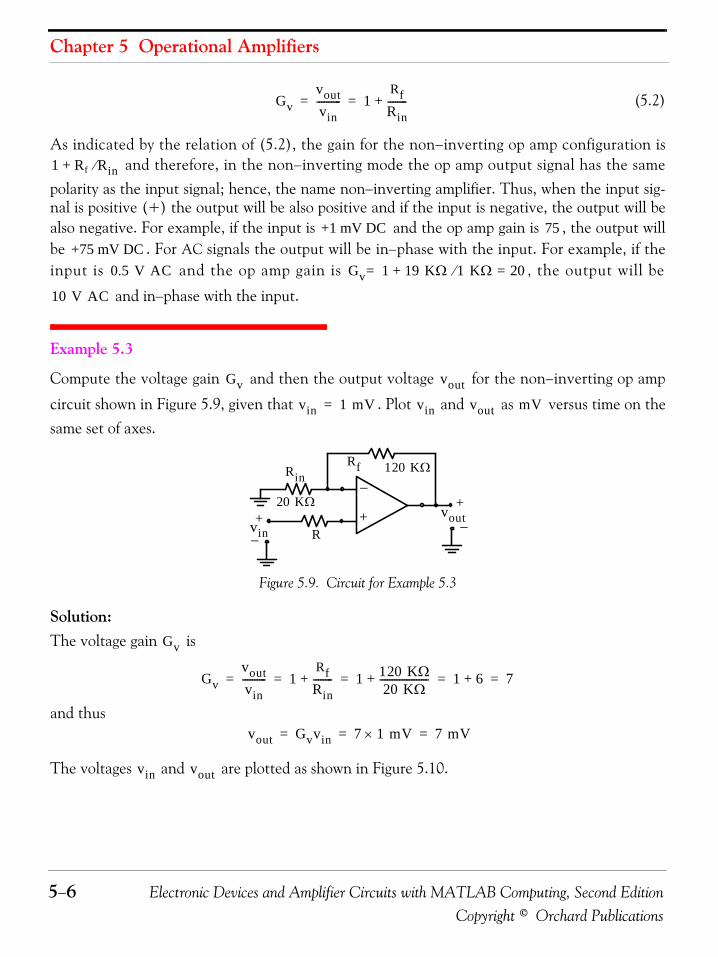
Chapter 5 Operational Amplifiers
5−6 Electronic Devices and Amplifier Circuits with MATLAB Computing, Second EditionCopyright © Orchard Publications
(5.2)
As indicated by the relation of (5.2), the gain for the non−inverting op amp configuration is and therefore, in the non−inverting mode the op amp output signal has the same
polarity as the input signal; hence, the name non−inverting amplifier. Thus, when the input sig-nal is positive (+) the output will be also positive and if the input is negative, the output will bealso negative. For example, if the input is and the op amp gain is , the output willbe . For AC signals the output will be in−phase with the input. For example, if theinput is and the op amp gain is , the output will be
and in−phase with the input.
Example 5.3
Compute the voltage gain and then the output voltage for the non−inverting op amp
circuit shown in Figure 5.9, given that . Plot and as versus time on thesame set of axes.
Figure 5.9. Circuit for Example 5.3
Solution:The voltage gain is
and thus
The voltages and are plotted as shown in Figure 5.10.
Gvvoutvin---------- 1
RfRin--------+= =
1 Rf Rin⁄+
+1 mV DC 75+75 mV DC
0.5 V AC Gv 1 19 KΩ 1 KΩ⁄+ 20==
10 V AC
Gv vout
vin 1 mV= vin vout mV
R−
+voutvin
RinRf
+ +
−
−
20 KΩ
120 KΩ
Gv
Gvvoutvin---------- 1
RfRin--------+ 1 120 KΩ
20 KΩ--------------------+ 1 6+ 7= = = = =
vout Gvvin 7 1× mV 7 mV= = =
vin vout
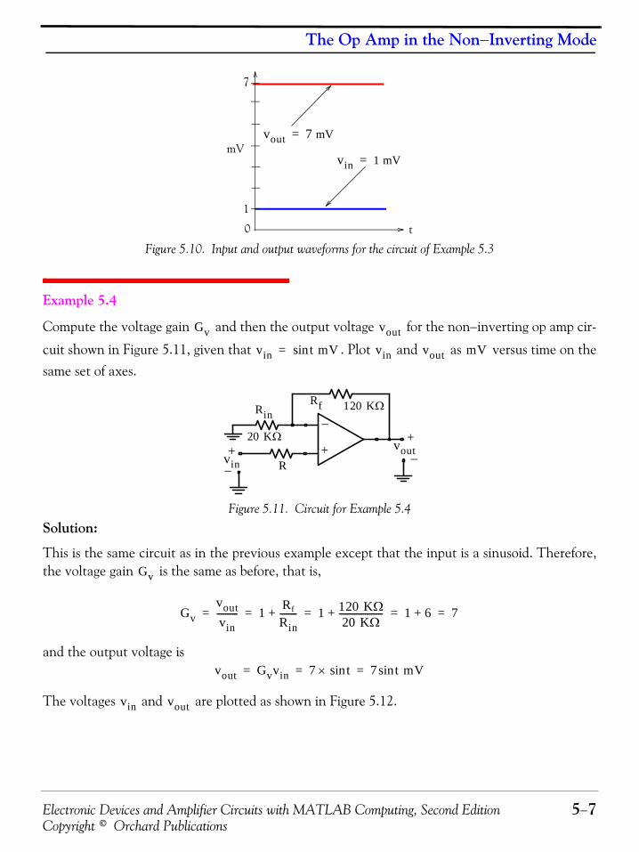
Electronic Devices and Amplifier Circuits with MATLAB Computing, Second Edition 5−7Copyright © Orchard Publications
The Op Amp in the Non−Inverting Mode
Figure 5.10. Input and output waveforms for the circuit of Example 5.3
Example 5.4
Compute the voltage gain and then the output voltage for the non−inverting op amp cir-
cuit shown in Figure 5.11, given that . Plot and as versus time on thesame set of axes.
Figure 5.11. Circuit for Example 5.4
Solution:
This is the same circuit as in the previous example except that the input is a sinusoid. Therefore,the voltage gain is the same as before, that is,
and the output voltage is
The voltages and are plotted as shown in Figure 5.12.
0
7
1
mV
t
vin 1 mV=
vout 7 mV=
Gv vout
vin t sin mV= vin vout mV
R−
+voutvin
RinRf
+ +
−
−
20 KΩ
120 KΩ
Gv
Gvvoutvin---------- 1 Rf
Rin--------+ 1 120 KΩ
20 KΩ--------------------+ 1 6+ 7= = = = =
vout Gvvin 7 tsin× 7 t sin mV= = =
vin vout

Chapter 5 Operational Amplifiers
5−8 Electronic Devices and Amplifier Circuits with MATLAB Computing, Second EditionCopyright © Orchard Publications
Figure 5.12. Input and output waveforms for the circuit of Example 5.4
Quite often an op amp is connected as shown in Figure 5.13.
Figure 5.13. Circuit of unity gain op amp
For the circuit of Figure 5.13, the voltage gain is
and thus
For this reason, the op amp circuit of Figure 5.13 it is called unity gain amplifier. For example, ifthe input voltage is the output will also be , and if the input voltage is
, the output will also be . The unity gain op amp is used to provide a veryhigh resistance between a voltage source and the load connected to it. An application is pre-sented in Example 5.8.
5.5 Active FiltersAn active filter is an electronic circuit consisting of an amplifier and other devices such as resistorsand capacitors. In contrast, a passive filter is a circuit which consists of passive devices such asresistors, capacitors and inductors. Operational amplifiers are used extensively as active filters.
A low−pass filter transmits (passes) all frequencies below a critical (cutoff) frequency denoted as, and attenuates (blocks) all frequencies above this cutoff frequency. An op amp low−pass filter
0 2 4 6 8 1 0 1 2 1 4-8
-6
-4
-2
0
2
4
6
8
mV
vin tsin=
vout 7 tsin=
0 t
−R
+vin
vout+ +
−
−
Gv
Gvvoutvin---------- 1= =
vout vin=
5 mV DC 5 mV DC2 mV AC 2 mV AC
ωC
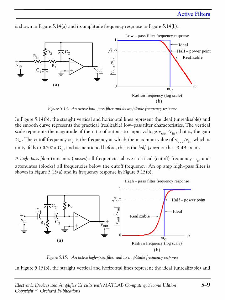
Electronic Devices and Amplifier Circuits with MATLAB Computing, Second Edition 5−9Copyright © Orchard Publications
Active Filters
is shown in Figure 5.14(a) and its amplitude frequency response in Figure 5.14(b).
Figure 5.14. An active low−pass filter and its amplitude frequency response
In Figure 5.14(b), the straight vertical and horizontal lines represent the ideal (unrealizable) andthe smooth curve represents the practical (realizable) low−pass filter characteristics. The verticalscale represents the magnitude of the ratio of output−to−input voltage , that is, the gain
. The cutoff frequency is the frequency at which the maximum value of which is
unity, falls to , and as mentioned before, this is the half−power or the point.
A high−pass filter transmits (passes) all frequencies above a critical (cutoff) frequency , andattenuates (blocks) all frequencies below the cutoff frequency. An op amp high−pass filter isshown in Figure 5.15(a) and its frequency response in Figure 5.15(b).
Figure 5.15. An active high−pass filter and its amplitude frequency response
In Figure 5.15(b), the straight vertical and horizontal lines represent the ideal (unrealizable) and
vinvout
b( )
a( )
R2Rin
C1
R1
C2
ωCRadian frequency (log scale)
Half power point–
Ideal
Realizable
1
0
3 2⁄
Low pass filter frequency response–
v out
v in⁄
ω
vout vin⁄
Gv ωc vout vin⁄
0.707 Gv× 3 dB–
ωc
vinvout
b( )
a( )
v out
v in⁄
High pass filter frequency response–
Half power point–
1
3 2⁄
ωC0
Radian frequency (log scale)
IdealRealizable
R2C1
R1
C2
C3
ω

Chapter 5 Operational Amplifiers
5−10 Electronic Devices and Amplifier Circuits with MATLAB Computing, Second EditionCopyright © Orchard Publications
the smooth curve represents the practical (realizable) high−pass filter characteristics. The verti-cal scale represents the magnitude of the ratio of output−to−input voltage , that is, the
gain . The cutoff frequency is the frequency at which the maximum value of
which is unity, falls to , i.e., the half−power or the point.
A band−pass filter transmits (passes) the band (range) of frequencies between the critical (cutoff)frequencies denoted as and , where the maximum value of which is unity, falls to
, while it attenuates (blocks) all frequencies outside this band. An op amp band−passfilter and its frequency response are shown below. An op amp band−pass filter is shown in Figure5.16(a) and its frequency response in Figure 5.16(b).
A band−elimination or band−stop or band−rejection filter attenuates (rejects) the band (range) offrequencies between the critical (cutoff) frequencies denoted as and , where the maximumvalue of which is unity, falls to , while it transmits (passes) all frequencies outsidethis band. An op amp band−stop filter is shown in Figure 5.17(a) and its frequency response inFigure 5.17(b).
Figure 5.16. An active band−pass filter and its amplitude frequency response
vout vin⁄
Gv ωc vout vin⁄
0.707 Gv× 3 dB–
ω1 ω2 Gv
0.707 Gv×
ω1 ω2
Gv 0.707 Gv×
1 02
1 03
1 04
0
2
4
6
8
1 0
vinvout
b( )
a( )
Radian frequency (log scale)
ωω1 ω2
v out
v in⁄
1
3 2⁄
0
Half power points–
IdealRealizable
R2
C1
R1
C2R3

Electronic Devices and Amplifier Circuits with MATLAB Computing, Second Edition 5−11Copyright © Orchard Publications
Analysis of Op Amp Circuits
Figure 5.17. An active band−elimination filter and its amplitude frequency response
5.6 Analysis of Op Amp CircuitsThe procedure for analyzing an op amp circuit (finding voltages, currents and power) is the sameas for the other circuits which we have studied thus far. That is, we can apply Ohm’s law, KCLand KVL, superposition, Thevenin’s and Norton’s theorems. When analyzing an op amp circuit,we must remember that, for all practical purposes, in any op−amp:
a. The currents into both input terminals are zero
b. The voltage difference between the input terminals of an op amp is zero
c. For circuits containing op amps, we will assume that the reference (ground) is the common terminal ofthe two power supplies. For simplicity, the terminals of the power supplies will not be shown.
In this section we will provide several examples to illustrate the analysis of op amp circuits withoutbeing concerned about its internal operation; this will be discussed in a later section.
vinvout
a( )
b( )
v out
v in⁄
1
3 2⁄
0
Half power points–
Radian frequency (log scale)
ω1 ω2ω
Ideal
Realizable
R2
C1
R1
C2
R3
C3
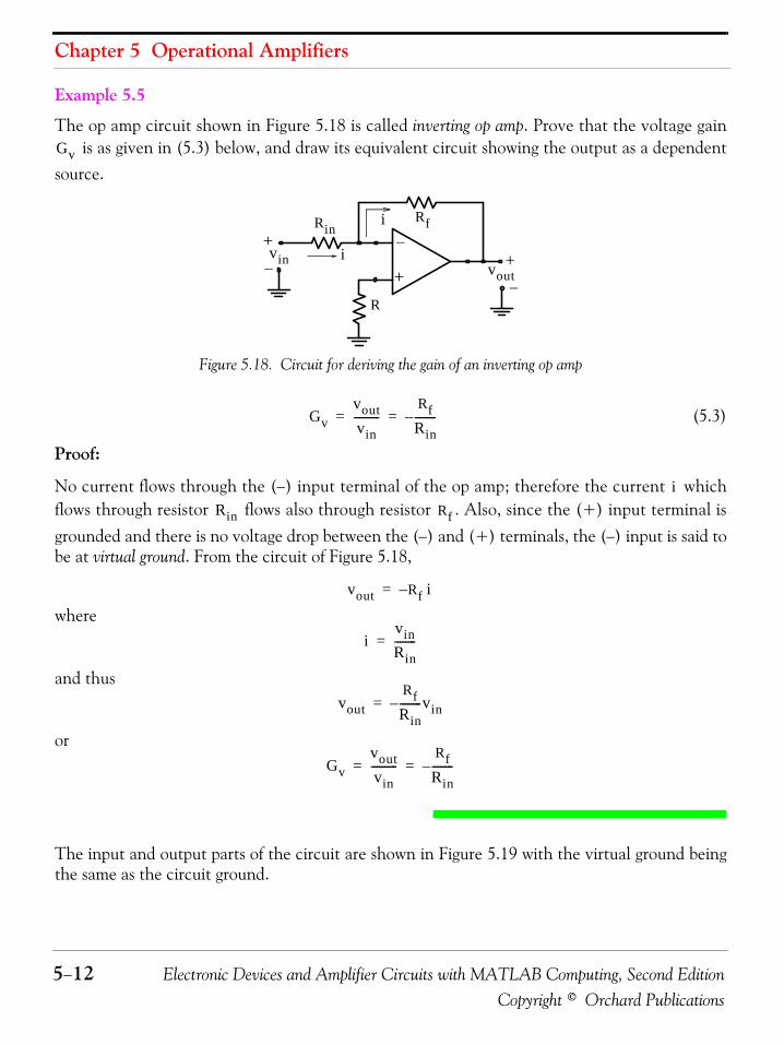
Chapter 5 Operational Amplifiers
5−12 Electronic Devices and Amplifier Circuits with MATLAB Computing, Second EditionCopyright © Orchard Publications
Example 5.5
The op amp circuit shown in Figure 5.18 is called inverting op amp. Prove that the voltage gain is as given in (5.3) below, and draw its equivalent circuit showing the output as a dependent
source.
Figure 5.18. Circuit for deriving the gain of an inverting op amp
(5.3)
Proof:
No current flows through the (−) input terminal of the op amp; therefore the current whichflows through resistor flows also through resistor . Also, since the (+) input terminal isgrounded and there is no voltage drop between the (−) and (+) terminals, the (−) input is said tobe at virtual ground. From the circuit of Figure 5.18,
where
and thus
or
The input and output parts of the circuit are shown in Figure 5.19 with the virtual ground beingthe same as the circuit ground.
Gv
+
−
R
+
−− +vin
Rf
vout
Rin
i
i
Gvvoutvin----------
RfRin--------–= =
iRin Rf
vout Rf i–=
ivinRin--------=
voutRfRin--------– vin=
Gvvoutvin----------
RfRin--------–= =

Electronic Devices and Amplifier Circuits with MATLAB Computing, Second Edition 5−13Copyright © Orchard Publications
Analysis of Op Amp Circuits
Figure 5.19. Input and output parts for the inverting op amp
These two circuits are normally drawn with the output as a dependent source as shown in Figure5.20. This is the equivalent circuit of the inverting op amp and the dependent source is a VoltageControlled Voltage Source (VCVS).*
Figure 5.20. Equivalent circuit for the inverting op amp
Example 5.6
The op amp circuit shown in Figure 5.21 is called non−inverting op amp. Prove that the voltage gain is as given in (5.4) below, and draw its equivalent circuit showing the output as a dependent
source.
Figure 5.21. Circuit of non−inverting op amp
(5.4)
Proof:
Let the voltages at the (−) and (+) terminals be denoted as and respectively as shown inFigure 5.22.
* For a definition of dependent sources please refer to Circuit Analysis I with MATLAB Applications, ISBN 978−0−9709511−2−0.
+
−+
−−
+
i−
+vin voutRfRin
i
+−
−
+
vin Rinvout
RfRin-------vin
+
−
Gv
+
−
+ −−
+voutvin
RinRf
Gvvoutvin---------- 1
RfRin--------+= =
v1 v2

Chapter 5 Operational Amplifiers
5−14 Electronic Devices and Amplifier Circuits with MATLAB Computing, Second EditionCopyright © Orchard Publications
Figure 5.22. Non−inverting op amp circuit for derivation of (5.4)
By application of KCL at
or(5.5)
There is no potential difference between the (−) and (+) terminals; therefore, or
. Relation (5.5) then can be written as
Rearranging, we obtain(5.6)
Figure 5.23 shows the equivalent circuit of Figure 5.22. The dependent source of this equivalentcircuit is also a VCVS.
Figure 5.23. Equivalent circuit for the non−inverting op amp
+
−
+ −−
+
+ −RfRin
i1
i2
vin
vout
v1
v2
v1
i1 i2+ 0=
v1Rin--------
v1 vout–
Rf---------------------+ 0=
v1 v2– 0=
v1 v2 vin= =
vinRin--------
vin vout–
Rf-----------------------+ 0=
1Rin-------- 1
Rf-----+⎝ ⎠
⎛ ⎞ vinvoutRf
----------=
Gvvoutvin---------- 1
RfRin--------+= =
+
−−
+
+−
1RfRin-------+⎝ ⎠
⎛ ⎞ vinvoutvin

Electronic Devices and Amplifier Circuits with MATLAB Computing, Second Edition 5−15Copyright © Orchard Publications
Analysis of Op Amp Circuits
Example 5.7
If, in the non−inverting op amp circuit of Example 5.6, we replace with an open circuit
( ) and with a short circuit ( ), prove that the voltage gain is
(5.7)
and thus
Proof:
With open and shorted, the non−inverting amplifier of the previous example reduces tothe circuit of Figure 5.24.
Figure 5.24. Circuit of Figure 5.22 with open and shorted
The voltage difference between the (+) and (−) terminals is zero; then .
We will obtain the same result if we consider the non−inverting op amp gain
Then, letting , the gain reduces to and for this reason this circuit is called unity
gain amplifier or voltage follower. It is also called buffer amplifier because it can be used to “buffer”(isolate) one circuit from another when one “loads” the other as we will see on the next example.
Example 5.8
For the circuit of Figure 5.25:
a. With the load disconnected, compute the open circuit voltage
b. With the load connected, compute the voltage across the load
Rin
Rin ∞→ Rf Rf 0→ Gv
Gvvoutvin---------- 1= =
vout vin=
Rin Rf
+
−
+ −−
+voutvin
Rin Rf
vout vin=
Gvvoutvin---------- 1
RfRin--------+= =
Rf 0→ Gv 1=
Rload vab
vload Rload
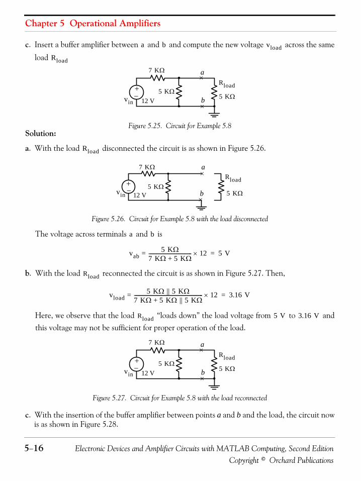
Chapter 5 Operational Amplifiers
5−16 Electronic Devices and Amplifier Circuits with MATLAB Computing, Second EditionCopyright © Orchard Publications
c. Insert a buffer amplifier between and and compute the new voltage across the same
load
Figure 5.25. Circuit for Example 5.8Solution:
a. With the load disconnected the circuit is as shown in Figure 5.26.
Figure 5.26. Circuit for Example 5.8 with the load disconnected
The voltage across terminals and is
b. With the load reconnected the circuit is as shown in Figure 5.27. Then,
Here, we observe that the load “loads down” the load voltage from to andthis voltage may not be sufficient for proper operation of the load.
Figure 5.27. Circuit for Example 5.8 with the load reconnected
c. With the insertion of the buffer amplifier between points a and b and the load, the circuit nowis as shown in Figure 5.28.
a b vload
Rload
+−
12 V×
×a
bvin
Rload
7 KΩ
5 KΩ5 KΩ
Rload
12 V ×
×a
b
7 KΩ
5 KΩ5 KΩ
+−vin
Rload
a b
vab5 KΩ
7 KΩ 5 KΩ+-----------------------------------= 12× 5 V=
Rload
vload5 KΩ || 5 KΩ
7 KΩ 5 KΩ || 5 KΩ+--------------------------------------------------------= 12× 3.16 V=
Rload 5 V 3.16 V
+−
12 V×
×a
bvin
Rload
7 KΩ
5 KΩ5 KΩ

Electronic Devices and Amplifier Circuits with MATLAB Computing, Second Edition 5−17Copyright © Orchard Publications
Analysis of Op Amp Circuits
Figure 5.28. Circuit for Example 5.8 with the insertion of a buffer op amp
From the circuit of Figure 5.28, we observe that the voltage across the load is as desired.
Example 5.9
The op amp circuit shown in Figure 5.29 is called summing circuit or summer because the output isthe summation of the weighted inputs. Prove that for this circuit,
(5.8)
Figure 5.29. Two−input summing op amp circuitProof:
We recall that the voltage across the (−) and (+) terminals is zero. We also observe that the (+)input is grounded, and thus the voltage at the (−) terminal is at “virtual ground”. Then, by appli-cation of KCL at the (−) terminal, we obtain
(5.9)
and solving for we obtain (5.8).
Alternately, we can apply the principle of superposition to derive this relation.
+−
12 V ×
×a
b
+
−
5 Vvin
7 KΩ
5 KΩ 5 KΩ
Rload vload vab 5 V= =−
+
5 V
vout Rfvin1Rin1----------
vin2Rin2----------+⎝ ⎠
⎛ ⎞–=
Rf
vout
Rin1
Rin2
vin2
vin1−+
+
++
−
−
R
vin1Rin1----------
vin2Rin2----------
voutRf
----------+ + 0=
vout
−
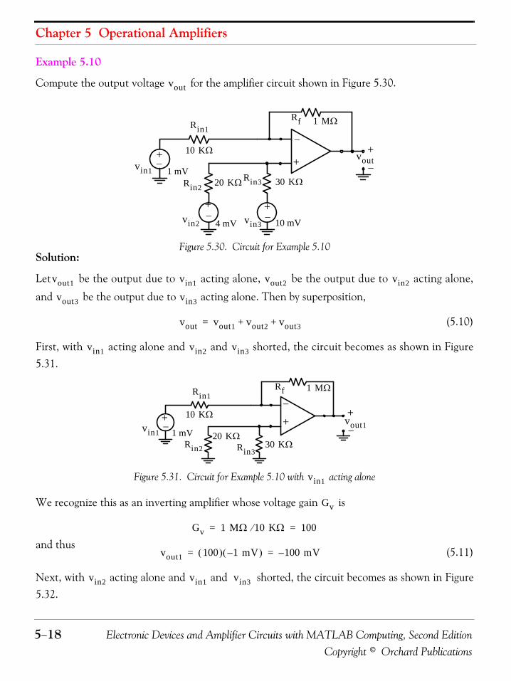
Chapter 5 Operational Amplifiers
5−18 Electronic Devices and Amplifier Circuits with MATLAB Computing, Second EditionCopyright © Orchard Publications
Example 5.10
Compute the output voltage for the amplifier circuit shown in Figure 5.30.
Figure 5.30. Circuit for Example 5.10Solution:
Let be the output due to acting alone, be the output due to acting alone,
and be the output due to acting alone. Then by superposition,
(5.10)
First, with acting alone and and shorted, the circuit becomes as shown in Figure5.31.
Figure 5.31. Circuit for Example 5.10 with acting alone
We recognize this as an inverting amplifier whose voltage gain is
and thus (5.11)
Next, with acting alone and and shorted, the circuit becomes as shown in Figure5.32.
vout
+−
−+
−1 mV
4 mV 10 mV
+
−+−
vout
vin3
vin1
vin2
Rin2
Rin1Rf 1 MΩ
10 KΩ
20 KΩ 30 KΩRin3
+
vout1 vin1 vout2 vin2
vout3 vin3
vout vout1 vout2 vout3+ +=
vin1 vin2 vin3
+− +
−+
1 mV
Rin1
10 KΩvin1
Rin220 KΩ
Rin330 KΩ
Rf 1 MΩ
vout1−
vin1
Gv
Gv 1 MΩ 10 KΩ⁄ 100= =
vout1 100( ) 1 mV–( ) 100 mV–= =
vin2 vin1 vin3

Electronic Devices and Amplifier Circuits with MATLAB Computing, Second Edition 5−19Copyright © Orchard Publications
Analysis of Op Amp Circuits
Figure 5.32. Circuit for Example 5.10 with acting alone
The circuit of Figure 5.32 as a non−inverting op amp whose voltage gain is
and the voltage at the plus (+) input is computed from the voltage divider circuit shown in Figure5.33.
Figure 5.33. Voltage divider circuit for the computation of with acting alone
Then,
and thus(5.12)
Finally, with acting alone and and shorted, the circuit becomes as shown in Figure5.34.
The circuit of Figure 5.34 is also a non−inverting op amp whose voltage gain is
and the voltage at the plus (+) input is computed from the voltage divider circuit shown in Figure5.35.
+−
+
−+
−
4 mV
Rin1
10 KΩ
Rf 1 MΩ
vout2Rin3
30 KΩ
vin2
Rin220 KΩ
vin2
Gv
Gv 1 1 MΩ+ 10 KΩ⁄ 101= =
+−
4 mV
+
−
30 KΩRin3
Rin220 KΩ
To v +( )
vin2
v +( ) vin2
v +( )
Rin3Rin2 Rin3+---------------------------- vin2× 30 KΩ
50 KΩ----------------- 4 mV× 2.4 mV= = =
vout2 101 2.4× mV 242.4 mV= =
vin3 vin1 vin2
Gv
Gv 1 1 MΩ+ 10 KΩ⁄ 101= =

Chapter 5 Operational Amplifiers
5−20 Electronic Devices and Amplifier Circuits with MATLAB Computing, Second EditionCopyright © Orchard Publications
Figure 5.34. Circuit for Example 5.10 with acting alone
Figure 5.35. Voltage divider circuit for the computation of with acting alone
From Figure 5.35,
and thus
Therefore, from (5.11), (5.12) and (5.13),
Example 5.11 For the circuit shown in Figure 5.36, derive an expression for the voltage gain in terms of the
external resistors , , , and .
Figure 5.36. Circuit for Example 5.11
+−
+
−+
−
10 mV
Rin1
10 KΩ
Rin220 KΩ
Rin3 30 KΩ
vin3
Rf 1 MΩ
vout3
vin3
+−
10 mV
+
−
30 KΩRin3Rin2
20 KΩ
To v +( )
vin3
v +( ) vin3
v +( )
Rin2Rin2 Rin3+---------------------------- vin2× 20 KΩ
50 KΩ----------------- 10 mV× 4 mV= = =
vout3 101 4× mV 404 mV= =
vout vout1 vout2 vout3+ + 100– 242.4 404+ + 546.4 mV= = =
Gv
R1 R2 R3 Rf
+
− +
−+
−R2
R3
RfR1
voutvin

Electronic Devices and Amplifier Circuits with MATLAB Computing, Second Edition 5−21Copyright © Orchard Publications
Analysis of Op Amp Circuits
Solution:
We apply KCL at nodes and as shown in Figure 5.37.
Figure 5.37. Application of KCL for the circuit of Example 5.11
At node :
or(5.13)
At node :
or (5.14)
and since , we rewrite (5.14) as
(5.15)
Equating the right sides of (5.13) and (5.15) we obtain
or
v1 v2
+
− +
−+
−R2
R3
RfR1
voutvin
v1
v2
v1v1 vin–
R1------------------
v1 vout–
Rf---------------------+ 0=
1R1------ 1
Rf-----+⎝ ⎠
⎛ ⎞ v1vinR1-------
voutRf
----------+=
R1 Rf+
R1Rf-----------------⎝ ⎠
⎛ ⎞ v1Rfvin R1vout+
R1Rf------------------------------------=
v1Rf vin R1vout+
R1 Rf+-------------------------------------=
v2v2 vin–
R2------------------
v2R3------+ 0=
v2R3vin
R2 R3+-------------------=
v2 v1=
v1R3vin
R2 R3+-------------------=
Rfvin R1vout+
R1 Rf+------------------------------------
R3vinR2 R3+-------------------=
Rf vin R1vout+R3vin
R2 R3+------------------- R1 Rf+( )=
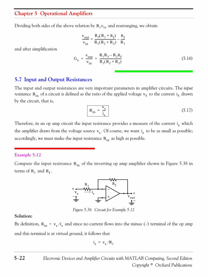
Chapter 5 Operational Amplifiers
5−22 Electronic Devices and Amplifier Circuits with MATLAB Computing, Second EditionCopyright © Orchard Publications
Dividing both sides of the above relation by and rearranging, we obtain
and after simplification
(5.16)
5.7 Input and Output ResistancesThe input and output resistances are very important parameters in amplifier circuits. The inputresistance of a circuit is defined as the ratio of the applied voltage to the current drawnby the circuit, that is,
(5.17)
Therefore, in an op amp circuit the input resistance provides a measure of the current which
the amplifier draws from the voltage source . Of course, we want to be as small as possible;
accordingly, we must make the input resistance as high as possible.
Example 5.12
Compute the input resistance of the inverting op amp amplifier shown in Figure 5.38 in
terms of and .
Figure 5.38. Circuit for Example 5.12
Solution:
By definition, and since no current flows into the minus (−) terminal of the op amp
and this terminal is at virtual ground, it follows that
R1vin
voutvin----------
R3 R1 Rf+( )
R1 R2 R3+( )------------------------------=
RfR1------–
Gvvoutvin----------
R1R3 R2Rf–
R1 R2 R3+( )-------------------------------= =
Rin vS iS
Rinvsis-----=
isvs is
Rin
Rin
R1 Rf
+
−+
−−
+
RfR1
vs voutis
Rin vs is⁄=
is vs R1⁄=
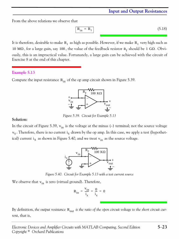
Electronic Devices and Amplifier Circuits with MATLAB Computing, Second Edition 5−23Copyright © Orchard Publications
Input and Output Resistances
From the above relations we observe that
(5.18)
It is therefore, desirable to make as high as possible. However, if we make very high such as, for a large gain, say , the value of the feedback resistor should be . Obvi-
ously, this is an impractical value. Fortunately, a large gain can be achieved with the circuit ofExercise 8 at the end of this chapter.
Example 5.13
Compute the input resistance of the op amp circuit shown in Figure 5.39.
Figure 5.39. Circuit for Example 5.13Solution:
In the circuit of Figure 5.39, is the voltage at the minus (−) terminal; not the source voltage
. Therefore, there is no current drawn by the op amp. In this case, we apply a test (hypothet-ical) current as shown in Figure 5.40, and we treat as the source voltage.
Figure 5.40. Circuit for Example 5.13 with a test current source
We observe that is zero (virtual ground). Therefore,
By definition, the output resistance is the ratio of the open circuit voltage to the short circuit cur-
rent, that is,
Rin R1=
R1 R1
10 MΩ 100 Rf 1 GΩ
Rin
+
−
−
+
Rf
voutvin
100 KΩ+
−
vin
vS iS
iX vin
+
−
−
+
Rf
vout
vin100 KΩ
iX
vin
Rinvinix------- 0
ix---- 0= = =
Rout

Chapter 5 Operational Amplifiers
5−24 Electronic Devices and Amplifier Circuits with MATLAB Computing, Second EditionCopyright © Orchard Publications
(5.19)
The output resistance is not the same as the load resistance. The output resistance provides ameasure of the change in output voltage when a load which is connected at the output terminalsdraws current from the circuit. It is desirable to have an op amp with very low output resistanceas illustrated by the following example.
Example 5.14
The output voltage of an op amp decreases by when a load is connected at the out-put terminals. Compute the output resistance .
Solution:Consider the output portion of the op amp shown in Figure 5.41.
Figure 5.41. Partial circuit for Example 5.14
With no load connected at the output terminals, we observe that
(5.20)
With a load connected at the output terminals, the load voltage is
(5.21)
and from (5.20) and (5.21)(5.22)
Therefore,
and solving for we obtain
From (5.22) we observe that as , and with (5.20), .
Routvocisc--------=
Rout
10% 5 KΩRout
+
− Rout
vout+
−
vout voc Gvvin= =
Rload vload
vloadRload
Rout Rload+------------------------------- vout×=
vloadRload
Rout Rload+------------------------------- Gvvin×=
vloadvOC------------ 0.9 5 KΩ
Rout 5 KΩ+--------------------------------= =
Rout Rout 555 Ω=
Rout 0→ vload Gvvin= vload vOC=
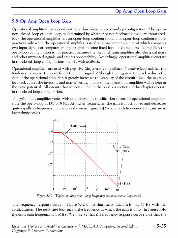
Electronic Devices and Amplifier Circuits with MATLAB Computing, Second Edition 5−25Copyright © Orchard Publications
Op Amp Open Loop Gain
5.8 Op Amp Open Loop Gain
Operational amplifiers can operate either a closed−loop or an open−loop configuration. The opera-tion, closed−loop or open−loop, is determined by whether or not feedback is used. Without feed-back the operational amplifier has an open−loop configuration. This open−loop configuration ispractical only when the operational amplifier is used as a comparator − a circuit which comparestwo input signals or compares an input signal to some fixed level of voltage. As an amplifier, theopen−loop configuration is not practical because the very high gain amplifies also electrical noiseand other unwanted signals, and creates poor stability. Accordingly, operational amplifiers operatein the closed−loop configurations, that is, with feedback.
Operational amplifiers are used with negative (degenerative) feedback. Negative feedback has thetendency to oppose (subtract from) the input signal. Although the negative feedback reduces thegain of the operational amplifier, it greatly increases the stability of the circuit. Also, the negativefeedback causes the inverting and non−inverting inputs to the operational amplifier will be kept atthe same potential. All circuits that we considered in the previous sections of this chapter operatein the closed loop configuration.
The gain of any amplifier varies with frequency. The specification sheets for operational amplifiersstate the open−loop at DC or . At higher frequencies, the gain is much lower and decreasesquite rapidly as frequency increases as shown in Figure 5.42 where both frequency and gain are inlogarithmic scales.
Figure 5.42. Typical op amp open−loop frequency response curve (log scales)
The frequency−response curve of Figure 5.42 shows that the bandwidth is only with thisconfiguration. The unity gain frequency is the frequency at which the gain is unity. In Figure 5.46the unity gain frequency is . We observe that the frequency response curve shows that the
0 Hz
1
f Hz( )
10
10610210 103104 105
1
102
103
104
105
Gain
3 dB point
frequencyUnity Gain
10 Hz
1 MHz
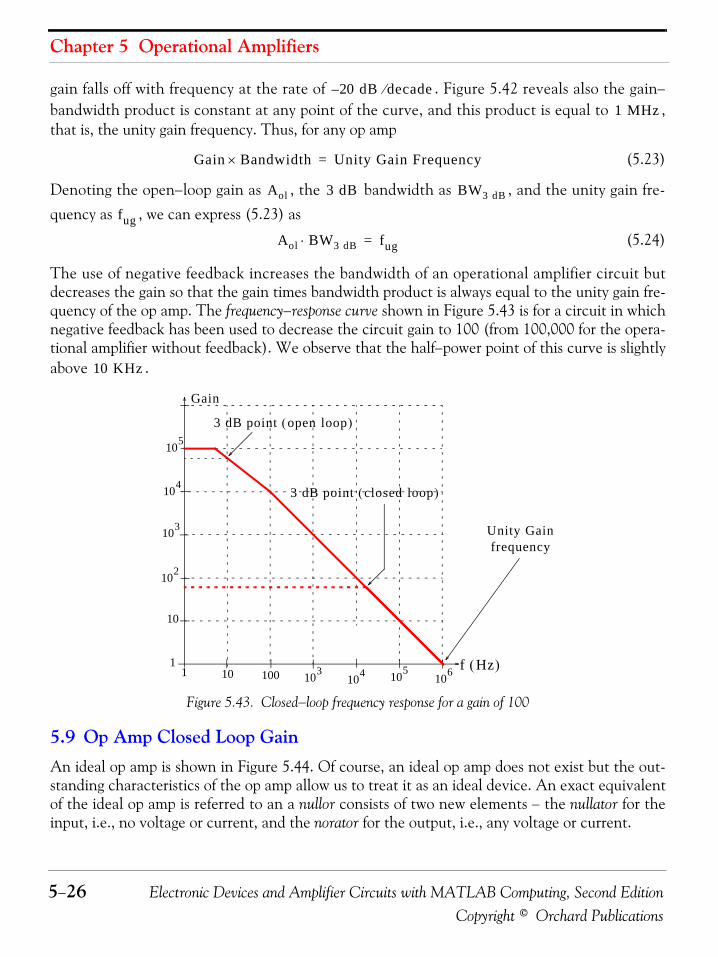
Chapter 5 Operational Amplifiers
5−26 Electronic Devices and Amplifier Circuits with MATLAB Computing, Second EditionCopyright © Orchard Publications
gain falls off with frequency at the rate of . Figure 5.42 reveals also the gain−bandwidth product is constant at any point of the curve, and this product is equal to ,that is, the unity gain frequency. Thus, for any op amp
(5.23)
Denoting the open−loop gain as , the bandwidth as , and the unity gain fre-quency as , we can express (5.23) as
(5.24)
The use of negative feedback increases the bandwidth of an operational amplifier circuit butdecreases the gain so that the gain times bandwidth product is always equal to the unity gain fre-quency of the op amp. The frequency−response curve shown in Figure 5.43 is for a circuit in whichnegative feedback has been used to decrease the circuit gain to 100 (from 100,000 for the opera-tional amplifier without feedback). We observe that the half−power point of this curve is slightlyabove .
Figure 5.43. Closed−loop frequency response for a gain of 100
5.9 Op Amp Closed Loop GainAn ideal op amp is shown in Figure 5.44. Of course, an ideal op amp does not exist but the out-standing characteristics of the op amp allow us to treat it as an ideal device. An exact equivalentof the ideal op amp is referred to an a nullor consists of two new elements − the nullator for theinput, i.e., no voltage or current, and the norator for the output, i.e., any voltage or current.
20 dB decade⁄–
1 MHz
Gain Bandwidth× Unity Gain Frequency=
Aol 3 dB BW3 dB
fug
Aol BW3 dB⋅ fug=
10 KHz
1 f Hz( )
10
10610010 103104 105
1
102
103
104
105
Gain
3 dB point open loop( )
frequency
3 dB point closed loop( )
Unity Gain
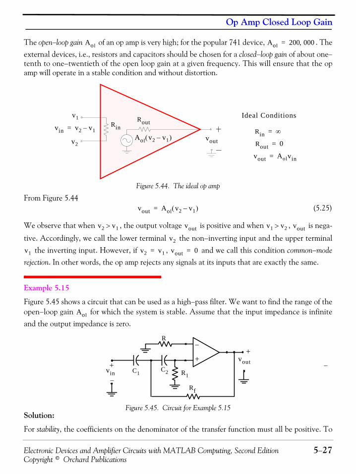
Electronic Devices and Amplifier Circuits with MATLAB Computing, Second Edition 5−27Copyright © Orchard Publications
Op Amp Closed Loop Gain
The open−loop gain of an op amp is very high; for the popular 741 device, . Theexternal devices, i.e., resistors and capacitors should be chosen for a closed−loop gain of about one−tenth to one−twentieth of the open loop gain at a given frequency. This will ensure that the opamp will operate in a stable condition and without distortion.
Figure 5.44. The ideal op amp
From Figure 5.44(5.25)
We observe that when , the output voltage is positive and when , is nega-
tive. Accordingly, we call the lower terminal the non−inverting input and the upper terminal the inverting input. However, if , and we call this condition common−mode
rejection. In other words, the op amp rejects any signals at its inputs that are exactly the same.
Example 5.15
Figure 5.45 shows a circuit that can be used as a high−pass filter. We want to find the range of theopen−loop gain for which the system is stable. Assume that the input impedance is infiniteand the output impedance is zero.
Figure 5.45. Circuit for Example 5.15Solution:
For stability, the coefficients on the denominator of the transfer function must all be positive. To
Aol Aol 200 000,=
RoutRinvin v2 v1–=
voutRin ∞=
Rout 0=
vout Aolvin=
Ideal Conditionsv1
v2Aol v2 v1–( )
vout Aol v2 v1–( )=
v2 v1> vout v1 v2> vout
v2
v1 v2 v1= vout 0=
Aol
+
−
+
−
+
Rf
R
vin
voutC1 C2 R1
−
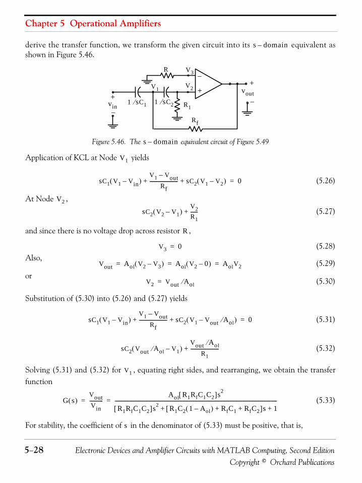
Chapter 5 Operational Amplifiers
5−28 Electronic Devices and Amplifier Circuits with MATLAB Computing, Second EditionCopyright © Orchard Publications
derive the transfer function, we transform the given circuit into its equivalent asshown in Figure 5.46.
Figure 5.46. The equivalent circuit of Figure 5.49
Application of KCL at Node yields
(5.26)
At Node ,
(5.27)
and since there is no voltage drop across resistor ,
(5.28)Also,
(5.29)or
(5.30)
Substitution of (5.30) into (5.26) and (5.27) yields
(5.31)
(5.32)
Solving (5.31) and (5.32) for , equating right sides, and rearranging, we obtain the transferfunction
(5.33)
For stability, the coefficient of in the denominator of (5.33) must be positive, that is,
s domain–
+
−
+
−
+
Rf
R
vin
vout
R11 sC1⁄ 1 sC2⁄
V3
V2V1
−
s domain–
V1
sC1 V1 Vin–( )V1 Vout–
Rf----------------------- sC2 V1 V2–( )+ + 0=
V2
sC2 V2 V1–( )V2R1------+
R
V3 0=
Vout Aol V2 V3–( ) Aol V2 0–( ) AolV2= = =
V2 Vout Aol⁄=
sC1 V1 Vin–( )V1 Vout–
Rf----------------------- sC2 V1 Vout Aol⁄–( )+ + 0=
sC2 Vout Aol⁄ V1–( )Vout Aol⁄
R1-----------------------+
V1
G s( )VoutVin-----------
Aol R1RfC1C2[ ]s2
R1RfC1C2[ ]s2 R1C2 1 Aol–( ) RfC1 RfC2+ +[ ]s 1+ +------------------------------------------------------------------------------------------------------------------------------------= =
s
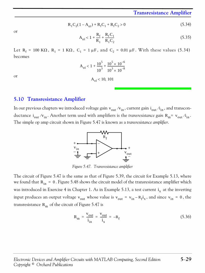
Electronic Devices and Amplifier Circuits with MATLAB Computing, Second Edition 5−29Copyright © Orchard Publications
Transresistance Amplifier
(5.34)or
(5.35)
Let , , , and . With these values (5.34)becomes
or
5.10 Transresistance Amplifier
In our previous chapters we introduced voltage gain , current gain , and transcon-
ductance . Another term used with amplifiers is the transresistance gain .The simple op amp circuit shown in Figure 5.47 is known as a transresistance amplifier.
Figure 5.47. Transresistance amplifier
The circuit of Figure 5.47 is the same as that of Figure 5.39, the circuit for Example 5.13, wherewe found that . Figure 5.48 shows the circuit model of the transresistance amplifier which
was introduced in Exercise 4 in Chapter 1. As in Example 5.13, a test current at the inverting
input produces an output voltage whose value is , and since , the
transresistance of the circuit of Figure 5.47 is
(5.36)
R1C2 1 Aol–( ) RfC1 RfC2+ + 0>
Aol 1RfR1------
Rf C1R1C2-------------+ +<
Rf 100 KΩ= R1 1 KΩ= C1 1 μF= C2 0.01 μF=
Aol 1 105
103-------- 105 10 6–×
103 10 8–×-------------------------+ +<
Aol 10 101,<
vout vin⁄ iout iin⁄
iout vin⁄ Rm vout iin⁄=
+
−
Rf
vout
vin+
+−
−
Rin 0=
ix
vout vout vin Rfix–= vin 0=
Rm
Rmvoutiin
----------voutix
---------- Rf–= = =

Chapter 5 Operational Amplifiers
5−30 Electronic Devices and Amplifier Circuits with MATLAB Computing, Second EditionCopyright © Orchard Publications
Figure 5.48. Transresistance circuit model
and the minus (−) sign indicates that them output voltage and the test current are out−of−phase with each other.
5.11 Closed Loop Transfer FunctionIn all of the previous sections of this chapter, the external devices in the op amp circuits wereresistors. However, several other circuits such as integrators, differentiators, and active filterscontain capacitors in addition to resistors. In this case it is convenient to denote devices in seriesas an impedance in the as , and in the as . Likewise, it is alsoconvenient to denote devices in parallel as or . Thus, for the inverting input mode,the closed loop transfer function is
(5.37)
where and are as shown in Figure 5.49.
Figure 5.49. The inverting amplifier
Example 5.16 Derive the closed−loop transfer function for the circuit of Figure 5.50.
Solution:
To derive the transfer function, we first convert the given circuit to its equivalent,and for convenience we denote the series devices as and the parallel devices as . Thecircuit then is as shown in Figure 5.51.
vinvoutRin
Rout
Rmiin
Rmvoutiin
----------iout 0=
=
ioutiin
vout ix 180°
s domain– Z s( ) jω domain– Z jω( )Y s( ) Y jω( )
G s( )
G s( )Vout s( )Vin s( )------------------
Zf s( )Z1 s( )-------------–= =
Zf s( ) Z1 s( )
+
−
Zf s( )
Z1 s( )Vin s( )Vout s( )
I s( )
++
−
−
s domain–
s domain–
Z1 s( ) Yf s( )
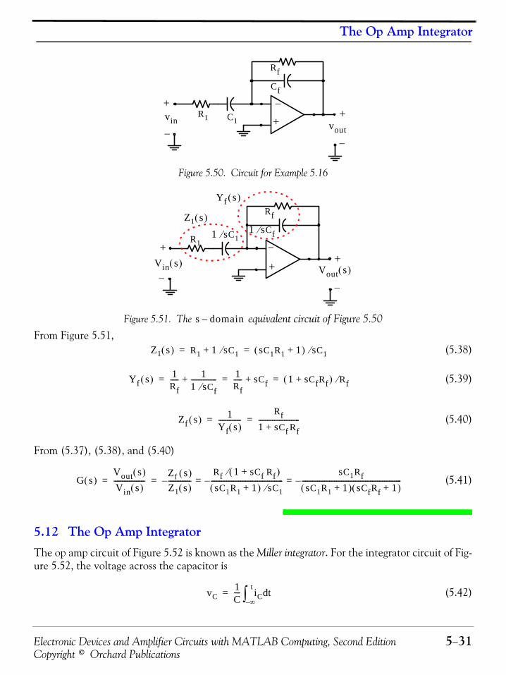
Electronic Devices and Amplifier Circuits with MATLAB Computing, Second Edition 5−31Copyright © Orchard Publications
The Op Amp Integrator
Figure 5.50. Circuit for Example 5.16
Figure 5.51. The equivalent circuit of Figure 5.50From Figure 5.51,
(5.38)
(5.39)
(5.40)
From (5.37), (5.38), and (5.40)
(5.41)
5.12 The Op Amp IntegratorThe op amp circuit of Figure 5.52 is known as the Miller integrator. For the integrator circuit of Fig-ure 5.52, the voltage across the capacitor is
(5.42)
+
−R1
Rf
Cf
vin C1
+
−−
+vout
+
−R1
Rf
Yf s( )
Vin s( )+
−−
+
1 sCf⁄1 sC1⁄
Vout s( )
Z1 s( )
s domain–
Z1 s( ) R1 1 sC1⁄+ sC1R1 1+( ) sC1⁄= =
Yf s( ) 1Rf----- 1
1 sCf⁄---------------+ 1
Rf----- sCf+ 1 sCfRf+( ) Rf⁄= = =
Zf s( ) 1Yf s( )-------------
Rf1 sCf Rf+------------------------= =
G s( )Vout s( )
Vin s( )------------------
Zf s( )Z1 s( )-------------
Rf 1 sCf Rf+( )⁄
sC1R1 1+( ) sC1⁄------------------------------------------
sC1RfsC1R1 1+( ) sCfRf 1+( )
----------------------------------------------------------–=–=–= =
vC1C---- iC td
∞–
t∫=
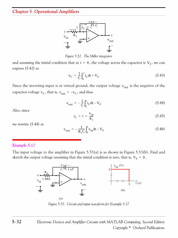
Chapter 5 Operational Amplifiers
5−32 Electronic Devices and Amplifier Circuits with MATLAB Computing, Second EditionCopyright © Orchard Publications
Figure 5.52. The Miller integrator
and assuming the initial condition that at , the voltage across the capacitor is , we canexpress (5.42) as
(5.43)
Since the inverting input is at virtual ground, the output voltage is the negative of the
capacitor voltage , that is, , and thus
(5.44)
Also, since(5.45)
we rewrite (5.44) as(5.46)
Example 5.17
The input voltage to the amplifier in Figure 5.53(a) is as shown in Figure 5.53(b). Find andsketch the output voltage assuming that the initial condition is zero, that is, .
Figure 5.53. Circuit and input waveform for Example 5.17
iC i=
vin vout
i C
R1
t 0= V0
vC1C---- iC td
0
t∫ V0+=
vout
vC vout vC–=
vout1C---- iC td
0
t∫– V0–=
iC ivinR1-------= =
vout1
R1C---------- vin td
0
t∫– V0–=
V0 0=
vin vout
1 MΩ
vin V( )
t s( )
2
3
a( )
b( )
1 μFR1
C
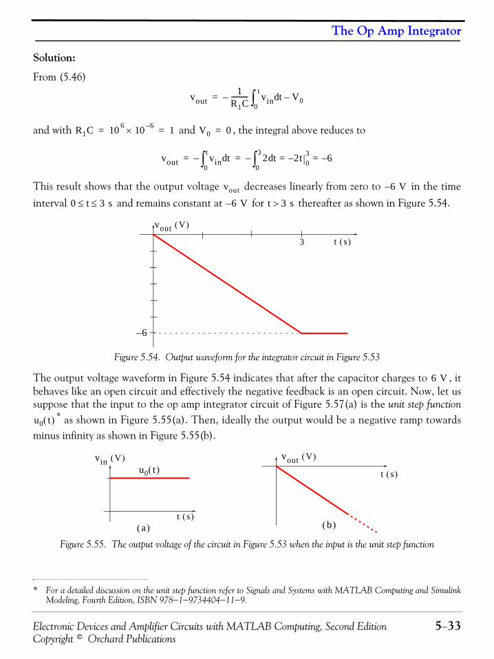
Electronic Devices and Amplifier Circuits with MATLAB Computing, Second Edition 5−33Copyright © Orchard Publications
The Op Amp Integrator
Solution:
From (5.46)
and with and , the integral above reduces to
This result shows that the output voltage decreases linearly from zero to in the timeinterval and remains constant at for thereafter as shown in Figure 5.54.
Figure 5.54. Output waveform for the integrator circuit in Figure 5.53
The output voltage waveform in Figure 5.54 indicates that after the capacitor charges to , itbehaves like an open circuit and effectively the negative feedback is an open circuit. Now, let ussuppose that the input to the op amp integrator circuit of Figure 5.57(a) is the unit step function
* as shown in Figure 5.55(a). Then, ideally the output would be a negative ramp towardsminus infinity as shown in Figure 5.55(b).
Figure 5.55. The output voltage of the circuit in Figure 5.53 when the input is the unit step function
* For a detailed discussion on the unit step function refer to Signals and Systems with MATLAB Computing and SimulinkModeling, Fourth Edition, ISBN 978−1−9734404−11−9.
vout1
R1C---------- vin td
0
t∫– V0–=
R1C 10 6 10 6–× 1= = V0 0=
vout vin td0
t∫– 2 td
0
3∫ 2– t 0
3 6–= =–= =
vout 6 V–
0 t 3 s≤ ≤ 6 V– t 3 s>
t s( )
vout V( )
3
6–
6 V
u0 t( )
u0 t( )
t s( )a( )
vin V( )
t s( )
vout V( )
b( )

Chapter 5 Operational Amplifiers
5−34 Electronic Devices and Amplifier Circuits with MATLAB Computing, Second EditionCopyright © Orchard Publications
In reality, the output voltage saturates at the power supply voltage of the op amp, typically depending on the polarity of the input DC signal. This problem can be rectified if we place afeedback resistor in parallel with the capacitor, and in this case the circuit behaves like a low−
pass filter as shown in Exercise 13 at the end of this chapter. This feedback resistor should be atleast as large as the input resistance .
Example 5.18
The input voltage to the amplifier in Figure 5.56(a) is as shown in Figure 5.56(b). Find andsketch the output voltage for the interval assuming that the initial condition is zero,that is, .
Figure 5.56. Circuit and input waveform for Example 5.18Solution:
This is the same circuit and input voltage waveform as in Example 5.17 except that a feedback resistor has been added and the capacitor value was changed to to simplify thecomputations. Since it is stated that the initial condition is zero, the capacitor charges in accor-dance with the relation
(5.47)where
for . The output voltage for this time interval is
and at
15 V±
Rf
R1
0 t 10 s≤ ≤V0 0=
vin vout
1 MΩ
vin V( )
t s( )
2
3
a( ) b( )
0.2 μF
Rf
R1
5 MΩ
C
i
5 MΩ0.2 μF
vC V∞ 1 e1 RfC⁄( )t–
–( )=
V∞ iRf–vinR1-------Rf–
2–1 MΩ-------------- 5 MΩ× 10V–= = = =
0 t 3 s≤ ≤
vout vC– 10 1 e1 RfC⁄( ) t–
–( )–= =
t 3 s=
vout t 3 s=10 1 e 3 1⁄––( )– 10 1 0.05–( )– 10 0.95( )– 9.5 V–= = = =

Electronic Devices and Amplifier Circuits with MATLAB Computing, Second Edition 5−35Copyright © Orchard Publications
The Op Amp Differentiator
At
The output waveform is shown in Figure 5.57.
Figure 5.57. Output waveform for the circuit of Example 5.18
As we can see from Figure 5.57, the addition of the feedback resistor makes the circuit of Figure5.56 somewhat less than an ideal integrator.
5.13 The Op Amp DifferentiatorThe op amp can also be configured to perform differentiation. The basic differentiator circuit isshown in Figure 5.58.
Figure 5.58. Basic differentiator circuit
We observe that the right side of the capacitor is virtually grounded and therefore the currentthrough the capacitor is
Also,
(5.48)
and we observe that the output voltage is the derivative of the input voltage .
t 10 s=
vout t 10 s=vout t 3 s=
e 1 RC⁄( ) t–× 10e 10 1⁄–– 10 4.54 10 5–××– 45.4 μV–= = = =
t s( )
vout V( )3
9.5–
10
Rf
vin
C+
−−
+vout
iC
iC
+
−
iC CdvCdt
--------- Cdvindt
----------= =
vout Rf iC–=
vout RfCdvindt
----------–=
vout vin
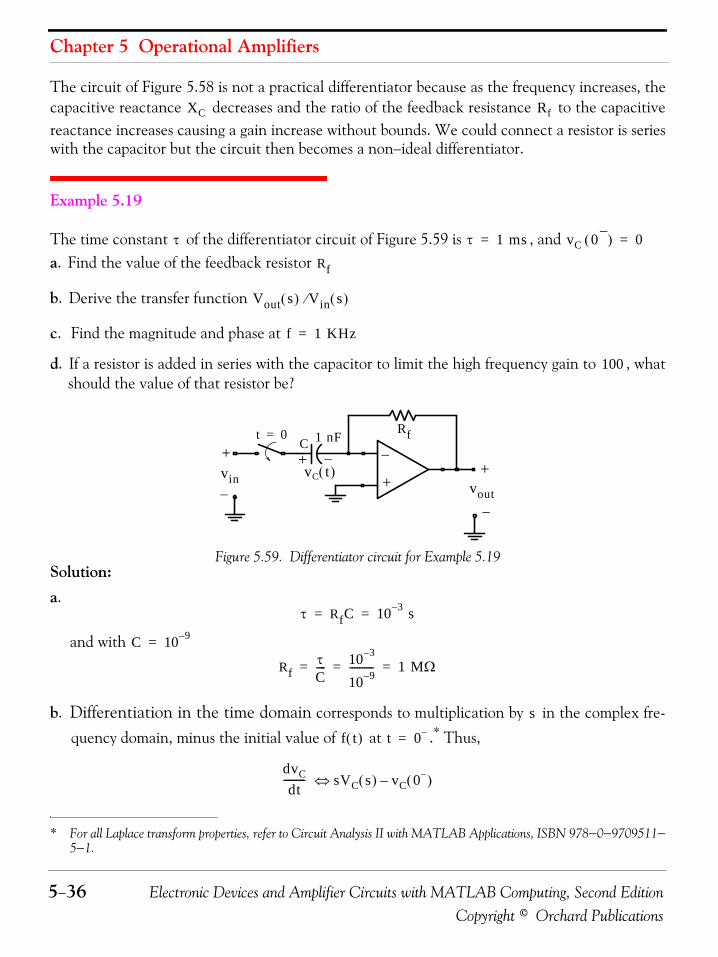
Chapter 5 Operational Amplifiers
5−36 Electronic Devices and Amplifier Circuits with MATLAB Computing, Second EditionCopyright © Orchard Publications
The circuit of Figure 5.58 is not a practical differentiator because as the frequency increases, thecapacitive reactance decreases and the ratio of the feedback resistance to the capacitivereactance increases causing a gain increase without bounds. We could connect a resistor is serieswith the capacitor but the circuit then becomes a non−ideal differentiator.
Example 5.19
The time constant of the differentiator circuit of Figure 5.59 is , and a. Find the value of the feedback resistor
b. Derive the transfer function
c. Find the magnitude and phase at
d. If a resistor is added in series with the capacitor to limit the high frequency gain to , whatshould the value of that resistor be?
Figure 5.59. Differentiator circuit for Example 5.19Solution:a.
and with
b. Differentiation in the time domain corresponds to multiplication by in the complex fre-
quency domain, minus the initial value of at .* Thus,
* For all Laplace transform properties, refer to Circuit Analysis II with MATLAB Applications, ISBN 978−0−9709511−5−1.
XC Rf
τ τ 1 ms= vC 0 −( ) 0=
Rf
Vout s( ) Vin s( )⁄
f 1 KHz=
100
+
−
Rf
vin
t 0=
+
−−
+vout
1 nF
vC t( )
C+ −
τ RfC 10 3– s= =
C 10 9–=
RfτC---- 10 3–
10 9–---------- 1 MΩ= = =
s
f t( ) t 0−=
dvCdt
--------- sVC s( ) vC 0−( )–⇔
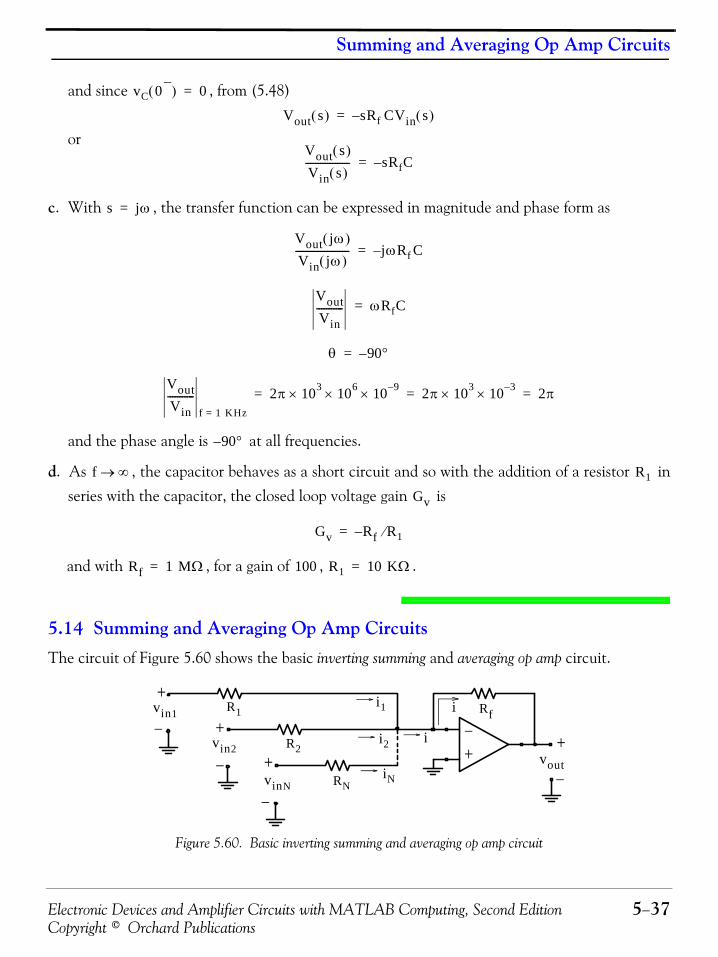
Electronic Devices and Amplifier Circuits with MATLAB Computing, Second Edition 5−37Copyright © Orchard Publications
Summing and Averaging Op Amp Circuits
and since , from (5.48)
or
c. With , the transfer function can be expressed in magnitude and phase form as
and the phase angle is at all frequencies.
d. As , the capacitor behaves as a short circuit and so with the addition of a resistor inseries with the capacitor, the closed loop voltage gain is
and with , for a gain of , .
5.14 Summing and Averaging Op Amp CircuitsThe circuit of Figure 5.60 shows the basic inverting summing and averaging op amp circuit.
Figure 5.60. Basic inverting summing and averaging op amp circuit
vC 0 −( ) 0=
Vout s( ) sRf CVin s( )–=
Vout s( )
Vin s( )------------------ sRfC–=
s jω=
Vout jω( )
Vin jω( )---------------------- jωRf C–=
VoutVin----------- ωRfC=
θ 90°–=
VoutVin-----------
f 1 KHz=
2π 103× 106× 10 9–× 2π 103× 10 3–× 2π= = =
90°–
f ∞→ R1
Gv
Gv Rf R1⁄–=
Rf 1 MΩ= 100 R1 10 KΩ=
Rfvin1
+
−
voutvinN RN
R1
R2vin2
ii1
i2
iN
i+
+ ++
−
−
−
−

Chapter 5 Operational Amplifiers
5−38 Electronic Devices and Amplifier Circuits with MATLAB Computing, Second EditionCopyright © Orchard Publications
In the circuit of 5.60, the total current is
where
Also
Then,
(5.49)
If all input resistances are equal, that is, if
the relation of (5.49) reduces to
(5.50)
If , relation (5.49) reduces further to
(5.51)
and this indicates that the circuit of Figure 5.60 can be used to find the negative sum of any num-ber of input voltages.
The circuit of Figure 5.60 can also be used to find the average value of all input voltages. Theratio is selected such that the sum of the input voltages is divided by the number of inputvoltages applied at the inverting input of the op amp.
The circuit of Figure 5.61 shows the basic non−inverting summing and non−inverting averaging opamp circuit. In Figure 5.61 the voltage sources and their series resistances
can be replaced by current sources whose values are
and their parallel resistances .* The circuit of Figure 5.61 can now be represented asin Figure 5.62.
* For voltage source with series resistance to current source with parallel resistance transformation please refer to CircuitAnalysis I with MATLAB Applications, ISBN 978−0−9709511−2−0
i i1 i2 … iN+ + +=
i1vin1R1
---------= i2vin2R2
---------= … iNvinNRN
----------=
vout Rfi– Rf i1 i2 … iN+ + +( )–= =
vout Rfi– Rf i1 i2 … iN+ + +( )–RfR1------vin1
RfR2------vin2 …
RfRN-------vinN+ + +⎝ ⎠
⎛ ⎞–= = =
R1 R2 … RN R= = = =
voutRfR----- vin1 vin2 … vinN+ + +( )–=
Rf R=
vout vin1 vin2 … vinN+ + +( )–=
Rf R⁄
vin1 vin2 … vinN, , ,
R1 R2 … RN, , ,
vin1 R1⁄ vin2 R2⁄ … vinN RN⁄, , ,
R1 R2 … RN, , ,

Electronic Devices and Amplifier Circuits with MATLAB Computing, Second Edition 5−39Copyright © Orchard Publications
Differential Input Op Amp
Figure 5.61. Basic non−inverting summing and averaging op amp circuit
Figure 5.62. Equivalent circuit for the circuit of Figure 5.61
In the circuit of Figure 5.62, the voltage at the non−inverting input is and thusthe output voltage is
(5.52)
5.15 Differential Input Op AmpThe circuit of Figure 5.63 is a differential input op amp.
Figure 5.63. Differential input op amp
Rf
vin1
+
−
vout
vinN
RN
R1
R2
vin2
+
+
++
−
−
−
−
R
+
−Rf
−
+vout
Req
V2
R
V2 V2 ReqIeq=
voutRfR----- 1+⎝ ⎠
⎛ ⎞ V2RfR----- 1+⎝ ⎠
⎛ ⎞ ReqIeq( )= =
+
−
Rf
−
+vout+
−
vin1 R2
R3
R1+
−vin2

Chapter 5 Operational Amplifiers
5−40 Electronic Devices and Amplifier Circuits with MATLAB Computing, Second EditionCopyright © Orchard Publications
The differential input configuration allows input signals to be applied simultaneously to bothinput terminals and produce an output of the difference between the input signals as shown inFigure 5.63. Differential input op amps are used in instrumentation circuits.
We will apply the superposition principle to derive an expression for the output voltage .
With the input voltage acting alone and grounded, the circuit of Figure 5.63 reduces tothat of Figure 5.64.
Figure 5.64. The circuit of Figure 5.63 with acting alone
The circuit of Figure 5.64 is an inverting amplifier and thus
(5.53)
Next, with the input voltage grounded and acting alone, the circuit of Figure 5.63reduces to that of Figure 5.65 and as indicated, we denote the voltage at the non−inverting inputas .
Figure 5.65. The circuit of Figure 5.67 with acting alone
Then, by the voltage division expression,
(5.54)
The circuit of Figure 5.65 is a non−inverting amplifier and thus
vout
vin1 vin2
+−
Rf
vout1
vin1
R2 R3
R1
++ −
−
vin1
vout1
RfR1------vin1–=
vin1 vin2
v2
+
−
Rf
+vout2+
−
R2
R3
R1
vin2
v2
−
vin2
v2R3
R2 R3+-------------------vin2=
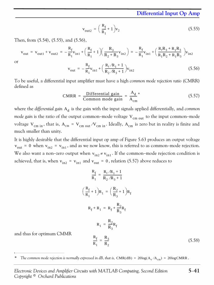
Electronic Devices and Amplifier Circuits with MATLAB Computing, Second Edition 5−41Copyright © Orchard Publications
Differential Input Op Amp
(5.55)
Then, from (5.54), (5.55), and (5.56),
or(5.56)
To be useful, a differential input amplifier must have a high common mode rejection ratio (CMRR)defined as
* (5.57)
where the differential gain is the gain with the input signals applied differentially, and common
mode gain is the ratio of the output common−mode voltage to the input common−mode
voltage , that is, . Ideally, is zero but in reality is finite andmuch smaller than unity.
It is highly desirable that the differential input op amp of Figure 5.63 produces an output voltage when , and as we now know, this is referred to as common−mode rejection.
We also want a non−zero output when . If the common−mode rejection condition is
achieved, that is, when and , relation (5.57) above reduces to
and thus for optimum CMMR(5.58)
* The common mode rejection is normally expressed in dB, that is, .
vout2RfR1------ 1+⎝ ⎠
⎛ ⎞ v2=
vout vout1 vout2+RfR1------vin1–
RfR1------ 1+⎝ ⎠
⎛ ⎞ R3R2 R3+-------------------vin2⎝ ⎠
⎛ ⎞+RfR1------vin1–
RfR3 R1R3+
R1R2 R1R3+--------------------------------⎝ ⎠
⎛ ⎞ vin2+= = =
voutRfR1------vin1–
Rf R1⁄ 1+
R2 R3⁄ 1+--------------------------⎝ ⎠
⎛ ⎞ vin2+=
CMRR Differential gainCommon mode gain------------------------------------------------------
AdAcm----------= =
CMR dB( ) 20 Av Acm⁄( )log 20 CMRRlog= =
Ad
Vcm out
Vcm in Acm Vcm out Vcm in⁄= Acm
vout 0= vin2 vin1=
vin2 vin1≠
vin2 vin1= vout 0=
RfR1------
Rf R1⁄ 1+
R2 R3⁄ 1+--------------------------=
RfR1------ 1+⎝ ⎠
⎛ ⎞ R1R2R3------ 1+⎝ ⎠
⎛ ⎞ Rf=
Rf R1+ RfR2R3------Rf+=
R1R2R3------Rf=
RfR1------
R3R2------=
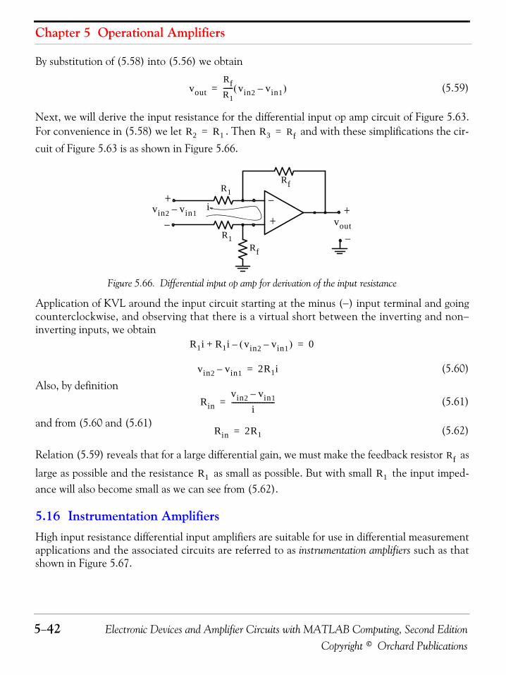
Chapter 5 Operational Amplifiers
5−42 Electronic Devices and Amplifier Circuits with MATLAB Computing, Second EditionCopyright © Orchard Publications
By substitution of (5.58) into (5.56) we obtain
(5.59)
Next, we will derive the input resistance for the differential input op amp circuit of Figure 5.63.For convenience in (5.58) we let . Then and with these simplifications the cir-cuit of Figure 5.63 is as shown in Figure 5.66.
Figure 5.66. Differential input op amp for derivation of the input resistance
Application of KVL around the input circuit starting at the minus (−) input terminal and goingcounterclockwise, and observing that there is a virtual short between the inverting and non−inverting inputs, we obtain
(5.60)Also, by definition
(5.61)
and from (5.60 and (5.61)(5.62)
Relation (5.59) reveals that for a large differential gain, we must make the feedback resistor as
large as possible and the resistance as small as possible. But with small the input imped-ance will also become small as we can see from (5.62).
5.16 Instrumentation AmplifiersHigh input resistance differential input amplifiers are suitable for use in differential measurementapplications and the associated circuits are referred to as instrumentation amplifiers such as thatshown in Figure 5.67.
voutRfR1------ vin2 vin1–( )=
R2 R1= R3 Rf=
+
−
Rf
−
+vout
R1Rf
R1+
−vin2 vin1– i
R1i R1i vin2 vin1–( )–+ 0=
vin2 vin1– 2R1i=
Rinvin2 vin1–
i-------------------------=
Rin 2R1=
Rf
R1 R1

Electronic Devices and Amplifier Circuits with MATLAB Computing, Second Edition 5−43Copyright © Orchard Publications
Instrumentation Amplifiers
Figure 5.67. High input resistance differential input op amp for use with instrumentation circuits
In the circuit of Figure 5.67 we have made the assumption that there is no current flowing at theinputs of amplifiers and and thus the same current flows through the resistive network. Thus,
(5.63)
We also have made the assumption that there is no voltage difference between the amplifiers and input terminals.
The output voltage of amplifier is
and with the second term on the right side of (5.63) the above relation can be expressed as
(5.64)
(5.65)
To find the output of amplifier we express (5.59) as
vout
R1v1 v2– +
−
R2
R2
R3
R3 R4
R4
v2
v1
vo1
vo2
A2
A1
A3I
+
+
+
+
+
−
−
−
−
−
A1 A2 R2 R1 R2––
Ivo1 v1–
R2-------------------
v1 v2–R1
----------------v2 v1–
R2----------------= = =
A1
A2
vo1 A1
vo1 R2I R1I R2I vo2+ + + R1 2R2+( )I vo2+= =
vo1 R1 2R2+( )v1 v2–
R1----------------⎝ ⎠
⎛ ⎞ vo2+ 12R2R1
---------+⎝ ⎠⎛ ⎞ v1 v2–( ) vo2+= =
vo1 vo2– 12R2R1
---------+⎝ ⎠⎛ ⎞ v1 v2–( )=
vo2 vo1– 12R2R1
---------+⎝ ⎠⎛ ⎞ v2 v1–( )=
vout A3
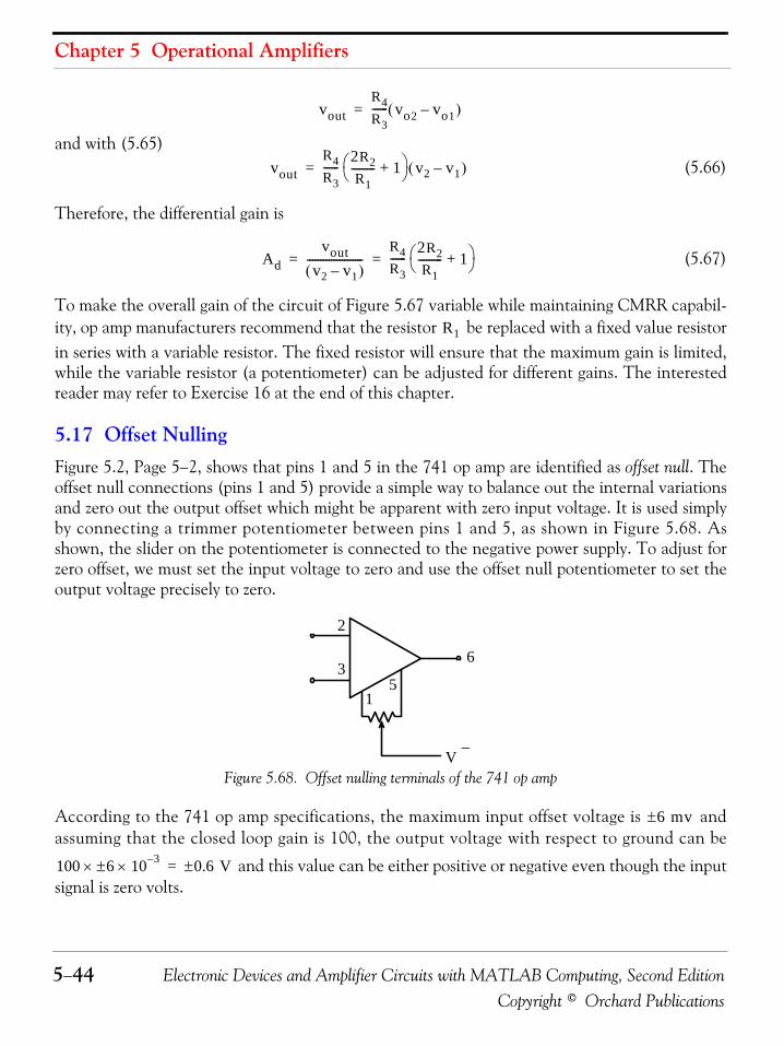
Chapter 5 Operational Amplifiers
5−44 Electronic Devices and Amplifier Circuits with MATLAB Computing, Second EditionCopyright © Orchard Publications
and with (5.65)(5.66)
Therefore, the differential gain is
(5.67)
To make the overall gain of the circuit of Figure 5.67 variable while maintaining CMRR capabil-ity, op amp manufacturers recommend that the resistor be replaced with a fixed value resistorin series with a variable resistor. The fixed resistor will ensure that the maximum gain is limited,while the variable resistor (a potentiometer) can be adjusted for different gains. The interestedreader may refer to Exercise 16 at the end of this chapter.
5.17 Offset NullingFigure 5.2, Page 5−2, shows that pins 1 and 5 in the 741 op amp are identified as offset null. Theoffset null connections (pins 1 and 5) provide a simple way to balance out the internal variationsand zero out the output offset which might be apparent with zero input voltage. It is used simplyby connecting a trimmer potentiometer between pins 1 and 5, as shown in Figure 5.68. Asshown, the slider on the potentiometer is connected to the negative power supply. To adjust forzero offset, we must set the input voltage to zero and use the offset null potentiometer to set theoutput voltage precisely to zero.
Figure 5.68. Offset nulling terminals of the 741 op amp
According to the 741 op amp specifications, the maximum input offset voltage is andassuming that the closed loop gain is 100, the output voltage with respect to ground can be
and this value can be either positive or negative even though the inputsignal is zero volts.
voutR4R3------ vo2 vo1–( )=
voutR4R3------ 2R2
R1--------- 1+⎝ ⎠
⎛ ⎞ v2 v1–( )=
Advout
v2 v1–( )---------------------
R4R3------ 2R2
R1--------- 1+⎝ ⎠
⎛ ⎞= =
R1
1
3
2
6
5
V −
6± mv
100 6± 10 3–×× 0.6± V=
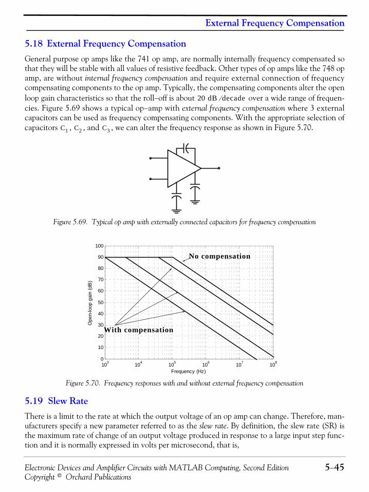
Electronic Devices and Amplifier Circuits with MATLAB Computing, Second Edition 5−45Copyright © Orchard Publications
External Frequency Compensation
5.18 External Frequency CompensationGeneral purpose op amps like the 741 op amp, are normally internally frequency compensated sothat they will be stable with all values of resistive feedback. Other types of op amps like the 748 opamp, are without internal frequency compensation and require external connection of frequencycompensating components to the op amp. Typically, the compensating components alter the openloop gain characteristics so that the roll−off is about over a wide range of frequen-cies. Figure 5.69 shows a typical op−amp with external frequency compensation where 3 externalcapacitors can be used as frequency compensating components. With the appropriate selection ofcapacitors , , and , we can alter the frequency response as shown in Figure 5.70.
Figure 5.69. Typical op amp with externally connected capacitors for frequency compensation
Figure 5.70. Frequency responses with and without external frequency compensation
5.19 Slew RateThere is a limit to the rate at which the output voltage of an op amp can change. Therefore, man-ufacturers specify a new parameter referred to as the slew rate. By definition, the slew rate (SR) isthe maximum rate of change of an output voltage produced in response to a large input step func-tion and it is normally expressed in volts per microsecond, that is,
20 dB decade⁄
C1 C2 C3
103
104
105
106
107
108
0
10
20
30
40
50
60
70
80
90
100
Frequency (Hz)
Ope
n-lo
op g
ain
(dB
)
No compensation
With compensation

Chapter 5 Operational Amplifiers
5−46 Electronic Devices and Amplifier Circuits with MATLAB Computing, Second EditionCopyright © Orchard Publications
(5.68)
Of course, relation (5.68) is the slope of the output voltage under maximum rate of change con-ditions. Typical slew rates range from to , and most internally compensatedop amps have slew rates in the order of . Figure 5.71 shows a step function of amplitude
applied to the input of a unity gain op amp, and the waveform at the output of this op amp.
Figure 5.71. The resultant slew rate when a step function is applied to a unity gain op amp
The linearly rising slew rate shown in Figure 5.71 will not be produced if the input voltage issmaller than that specified by the manufacturer. In this case, the slew rate will be a rising expo-nential such as the rising voltage across a capacitor. In most op amps the slew rate is set by thecharging rate of the frequency compensating capacitor and the output voltage is
(5.69)
where is the final value of the output voltage as shown in Figure 5.71, , and is the unity gain frequency as defined in (5.24), i.e., .
Figure 5.72. Plot for expression
5.20 Circuits with Op Amps and Non−Linear Devices Op amps are often used in circuits with non−linear devices. There are many circuits that can beformed with op amps and non−linear devices such as junction diodes, zener diodes, bipolar tran-
Slew Rate SRdvoutdtmax-------------= =
0.1 V μs⁄ 100 V μs⁄1 V μs⁄
10 V
vin V( ) vout V( )
t
Slew rate Slope=
t
10 10
−R
+
vin
vout+ +
−
−
vout Vf 1 eωugt–
–( )=
Vf ωug 2πfug= fug
Aol BW3 dB⋅ fug=
Δt 1 ωug⁄=
Vf
vout
t
vout Vf 1 eωugt–
–( )=

Electronic Devices and Amplifier Circuits with MATLAB Computing, Second Edition 5−47Copyright © Orchard Publications
Circuits with Op Amps and Non−Linear Devices
sistors, and MOSFETs. In this section we will introduce just a few.
Figure 5.73 shows a positive and negative voltage limiter circuit and its transfer characteristics. In thevoltage limiting circuit of Figure 5.73 the Zener diodes and limit the peak−to−peak valueof the output voltage. Thus, when the output voltage is positive, its value is limited to the value
where is the voltage drop across the forward−biased Zener diode and it is typically
about . Likewise, when the output voltage is positive, its value is limited to the value.
Figure 5.73. A positive and negative voltage limiter circuit and its transfer characteristics
Example 5.20
In the circuit of Figure 5.73, , , , and .
Describe the output waveforms when
a.
b.
c.
Solution:
Since this is an inverting amplifier, its gain is * and since we are interestedin peak values, the frequencies and phase angles are immaterial for this example. With the givenvalues, the output peaks on positive half−cycles are limited to
and the output peaks on negative half−cycles are limited to
* The gain is always expressed as a positive quantity. The minus sign simply implies inversion.
D1 D2
VZ1VF+ VF
0.7 VVZ2
VF+( )–
+−
Rf −
+vout
R1+
−
vin
voutD1 D2
Slope Rf R1⁄–=
VZ1VF+
VZ2VF+( )–vin
VZ1VZ2
6.3 V= = VF 0.7 V= R1 5 KΩ= Rf 100 KΩ=
vin 0.3 10 tsin=
vin 0.6 100cos t=
vin 3 1000 t π 6⁄+( )cos=
Rf R1⁄ 100 5⁄ 20= =
VZ1VF+ 6.3 0.7+ 7 V= =
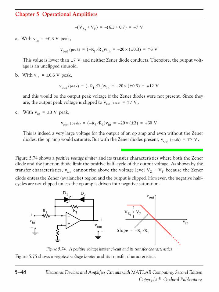
Chapter 5 Operational Amplifiers
5−48 Electronic Devices and Amplifier Circuits with MATLAB Computing, Second EditionCopyright © Orchard Publications
a. With peak,
This value is lower than and neither Zener diode conducts. Therefore, the output volt-age is an unclipped sinusoid.
b. With peak,
and this would be the output peak voltage if the Zener diodes were not present. Since theyare, the output peak voltage is clipped to .
c. With peak,
This is indeed a very large voltage for the output of an op amp and even without the Zenerdiodes, the op amp would saturate. But with the Zener diodes present, .
Figure 5.74 shows a positive voltage limiter and its transfer characteristics where both the Zenerdiode and the junction diode limit the positive half−cycle of the output voltage. As shown by thetransfer characteristics, cannot rise above the voltage level because the Zener
diode enters the Zener (avalanche) region and the output is clipped. However, the negative half−cycles are not clipped unless the op amp is driven into negative saturation.
Figure 5.74. A positive voltage limiter circuit and its transfer characteristics
Figure 5.75 shows a negative voltage limiter and its transfer characteristics.
VZ2VF+( )– 6.3 0.7+( )– 7– V= =
vin 0.3± V=
vout peak( ) Rf– R1⁄( )vin 20 0.3±( )×– 6+− V= = =
7 V±
vin 0.6± V=
vout peak( ) Rf– R1⁄( )vin 20 0.6±( )×– 12+− V= = =
vout peak( ) 7+− V=
vin 3± V=
vout peak( ) Rf– R1⁄( )vin 20 3±( )×– 60+− V= = =
vout peak( ) 7+− V=
vout VZ1VF+
+
−Rf
−
+vout
R1
vin
+
−vin
voutD1 D2
Slope Rf R1⁄–=
VZ1VF+
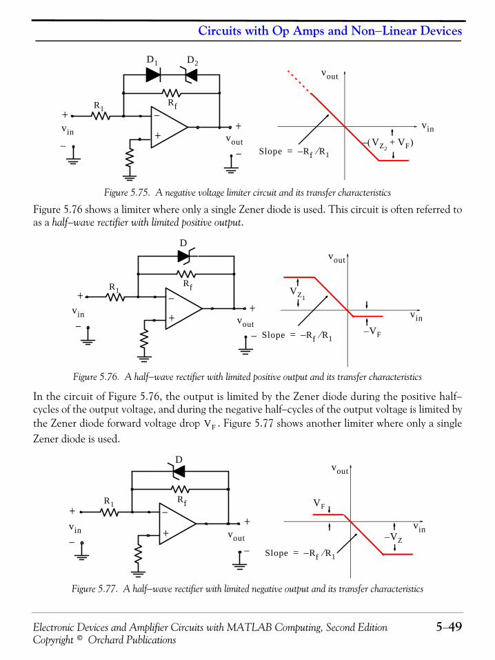
Electronic Devices and Amplifier Circuits with MATLAB Computing, Second Edition 5−49Copyright © Orchard Publications
Circuits with Op Amps and Non−Linear Devices
Figure 5.75. A negative voltage limiter circuit and its transfer characteristics
Figure 5.76 shows a limiter where only a single Zener diode is used. This circuit is often referred toas a half−wave rectifier with limited positive output.
Figure 5.76. A half−wave rectifier with limited positive output and its transfer characteristics
In the circuit of Figure 5.76, the output is limited by the Zener diode during the positive half−cycles of the output voltage, and during the negative half−cycles of the output voltage is limited bythe Zener diode forward voltage drop . Figure 5.77 shows another limiter where only a singleZener diode is used.
Figure 5.77. A half−wave rectifier with limited negative output and its transfer characteristics
+
−Rf
−
+vout
R1
vin
+
−
vin
vout
D1 D2
Slope Rf R1⁄–=VZ2
VF+( )–
+
−Rf
−
+vout
R1
vin
+
−vin
vout
D
Slope Rf R1⁄–=
VZ1
V– F
VF
+
−Rf
−
+vout
R1
vin
+
−vin
voutD
Slope Rf R1⁄–=
V– Z
VF
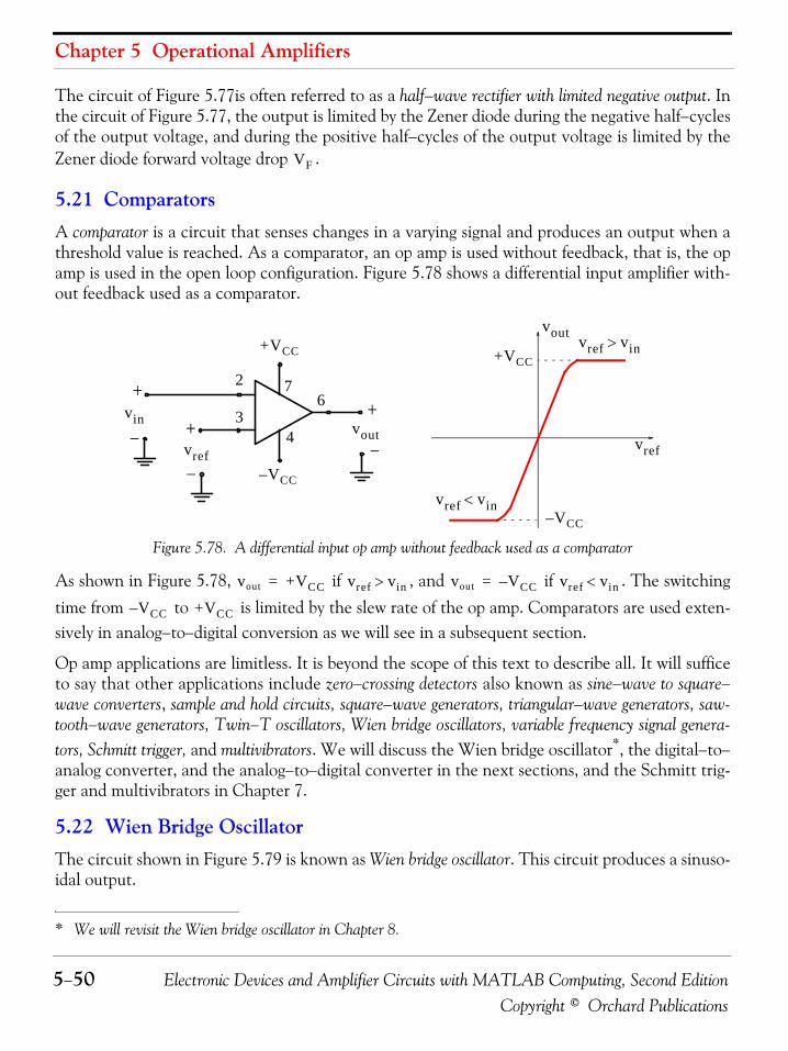
Chapter 5 Operational Amplifiers
5−50 Electronic Devices and Amplifier Circuits with MATLAB Computing, Second EditionCopyright © Orchard Publications
The circuit of Figure 5.77is often referred to as a half−wave rectifier with limited negative output. Inthe circuit of Figure 5.77, the output is limited by the Zener diode during the negative half−cyclesof the output voltage, and during the positive half−cycles of the output voltage is limited by theZener diode forward voltage drop .
5.21 ComparatorsA comparator is a circuit that senses changes in a varying signal and produces an output when athreshold value is reached. As a comparator, an op amp is used without feedback, that is, the opamp is used in the open loop configuration. Figure 5.78 shows a differential input amplifier with-out feedback used as a comparator.
Figure 5.78. A differential input op amp without feedback used as a comparator
As shown in Figure 5.78, if , and if . The switchingtime from to is limited by the slew rate of the op amp. Comparators are used exten-sively in analog−to−digital conversion as we will see in a subsequent section.
Op amp applications are limitless. It is beyond the scope of this text to describe all. It will sufficeto say that other applications include zero−crossing detectors also known as sine−wave to square−wave converters, sample and hold circuits, square−wave generators, triangular−wave generators, saw-tooth−wave generators, Twin−T oscillators, Wien bridge oscillators, variable frequency signal genera-tors, Schmitt trigger, and multivibrators. We will discuss the Wien bridge oscillator*, the digital−to−analog converter, and the analog−to−digital converter in the next sections, and the Schmitt trig-ger and multivibrators in Chapter 7.
5.22 Wien Bridge OscillatorThe circuit shown in Figure 5.79 is known as Wien bridge oscillator. This circuit produces a sinuso-idal output.
* We will revisit the Wien bridge oscillator in Chapter 8.
VF
−
+vout4
vin
+
− vref
vout
vref
+
−
2
3
76
+VCC
V– CC
+VCC
V– CC
vref vin<
vref vin>
vout +VCC= vref vin> vout V– CC= vref vin<
V– CC +VCC

Electronic Devices and Amplifier Circuits with MATLAB Computing, Second Edition 5−51Copyright © Orchard Publications
Wien Bridge Oscillator
Figure 5.79. The Wien bridge oscillator
Figure 5.79 shows that the Wien bridge oscillator uses two RC networks connected to the non−inverting input of the op amp to form a frequency selective feedback circuit and this causes oscil-lations to occur. It also amplifies the signal with two negative feedback resistors. The input signalto the non−inverting input is in phase with the output of the op amp at the particular frequency
(5.70)
provided that
and
The Wien bridge oscillator requires precision resistors and capacitors for reliable operation. Thefeedback signal at the non−inverting input of the op amp leads the output of the op amp at fre-quencies below and lags at frequencies above . The amount of negative feedback to the
inverting input of the op amp and amplitude can be adjusted with the potentiometer. Thediodes prevent excessive feedback amplitude.
Example 5.21
For the oscillator circuit in Figure 5.79 . What values of , , and arerequired to obtain a frequency of approximately ?
Solution:
The value of resistor must be . The values of capacitors , and must also beequal. From (5.70),
C2
50 KΩ
D1 D2R2C1R1
10KΩ
V
Vout
V
f01
2πRC---------------=
R R1 R2= =
C C1 C2= =
Vf0 V f0
50 KΩ
R1 100 KΩ= R2 C1 C2
1 KHz
R2 100 KΩ C1 C2
f0 1 KHz 12πRC--------------- 1
2π 105× C×-------------------------------= = =
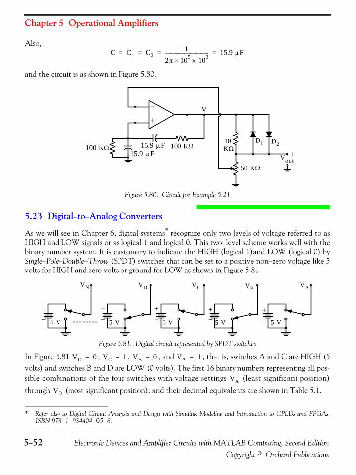
Chapter 5 Operational Amplifiers
5−52 Electronic Devices and Amplifier Circuits with MATLAB Computing, Second EditionCopyright © Orchard Publications
Also,
and the circuit is as shown in Figure 5.80.
Figure 5.80. Circuit for Example 5.21
5.23 Digital−to−Analog Converters
As we will see in Chapter 6, digital systems* recognize only two levels of voltage referred to asHIGH and LOW signals or as logical 1 and logical 0. This two−level scheme works well with thebinary number system. It is customary to indicate the HIGH (logical 1)and LOW (logical 0) bySingle−Pole−Double−Throw (SPDT) switches that can be set to a positive non−zero voltage like 5volts for HIGH and zero volts or ground for LOW as shown in Figure 5.81.
Figure 5.81. Digital circuit represented by SPDT switches
In Figure 5.81 , , , and , that is, switches A and C are HIGH (5volts) and switches B and D are LOW (0 volts). The first 16 binary numbers representing all pos-sible combinations of the four switches with voltage settings (least significant position)through (most significant position), and their decimal equivalents are shown in Table 5.1.
* Refer also to Digital Circuit Analysis and Design with Simulink Modeling and Introduction to CPLDs and FPGAs,ISBN 978−1−934404−05−8.
C C1 C21
2π 105× 103×------------------------------------ 15.9 μF= = = =
50 KΩ
D1 D215.9 μF 10KΩ
V
Vout
100 KΩ 100 KΩ15.9 μF
VN VD VC VAVB
5 V 5 V 5 V 5 V 5 V
VD 0= VC 1= VB 0= VA 1=
VA
VD
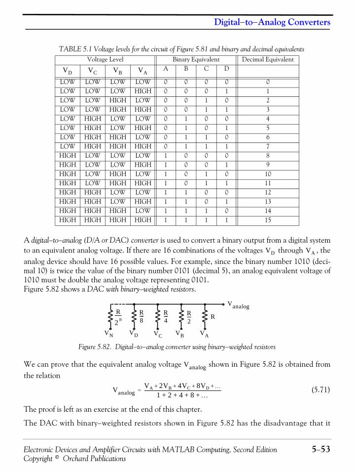
Electronic Devices and Amplifier Circuits with MATLAB Computing, Second Edition 5−53Copyright © Orchard Publications
Digital−to−Analog Converters
A digital−to−analog (D/A or DAC) converter is used to convert a binary output from a digital systemto an equivalent analog voltage. If there are 16 combinations of the voltages through , theanalog device should have 16 possible values. For example, since the binary number 1010 (deci-mal 10) is twice the value of the binary number 0101 (decimal 5), an analog equivalent voltage of1010 must be double the analog voltage representing 0101.Figure 5.82 shows a DAC with binary−weighted resistors.
Figure 5.82. Digital−to−analog converter using binary−weighted resistors
We can prove that the equivalent analog voltage shown in Figure 5.82 is obtained fromthe relation
(5.71)
The proof is left as an exercise at the end of this chapter.
The DAC with binary−weighted resistors shown in Figure 5.82 has the disadvantage that it
TABLE 5.1 Voltage levels for the circuit of Figure 5.81 and binary and decimal equivalentsVoltage Level Binary Equivalent Decimal Equivalent
A B C D
LOW LOW LOW LOW 0 0 0 0 0LOW LOW LOW HIGH 0 0 0 1 1LOW LOW HIGH LOW 0 0 1 0 2LOW LOW HIGH HIGH 0 0 1 1 3LOW HIGH LOW LOW 0 1 0 0 4LOW HIGH LOW HIGH 0 1 0 1 5LOW HIGH HIGH LOW 0 1 1 0 6LOW HIGH HIGH HIGH 0 1 1 1 7HIGH LOW LOW LOW 1 0 0 0 8HIGH LOW LOW HIGH 1 0 0 1 9HIGH LOW HIGH LOW 1 0 1 0 10HIGH LOW HIGH HIGH 1 0 1 1 11HIGH HIGH LOW LOW 1 1 0 0 12HIGH HIGH LOW HIGH 1 1 0 1 13HIGH HIGH HIGH LOW 1 1 1 0 14HIGH HIGH HIGH HIGH 1 1 1 1 15
VD VC VB VA
VD VA
Vanalog
VBVCVD VAVN
RR2----R
4----R
8----R
2 n------
Vanalog
VanalogVA 2VB 4VC 8VD …+ + + +
1 2 4 8 …+ + + +------------------------------------------------------------------------------=
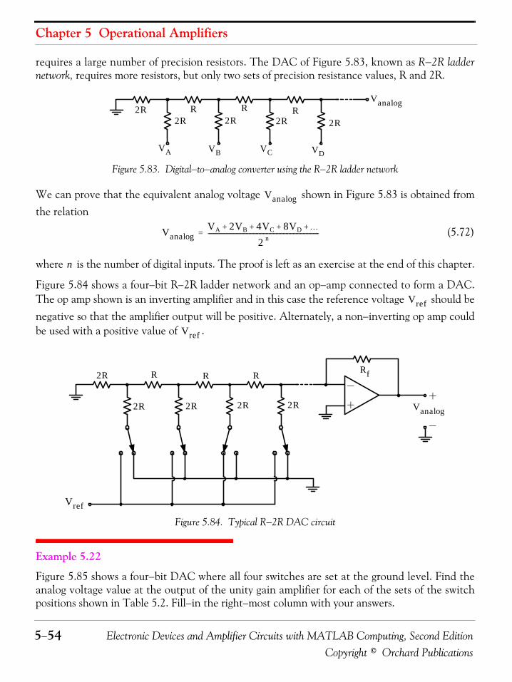
Chapter 5 Operational Amplifiers
5−54 Electronic Devices and Amplifier Circuits with MATLAB Computing, Second EditionCopyright © Orchard Publications
requires a large number of precision resistors. The DAC of Figure 5.83, known as R−2R laddernetwork, requires more resistors, but only two sets of precision resistance values, R and 2R.
Figure 5.83. Digital−to−analog converter using the R−2R ladder network
We can prove that the equivalent analog voltage shown in Figure 5.83 is obtained fromthe relation
(5.72)
where is the number of digital inputs. The proof is left as an exercise at the end of this chapter.
Figure 5.84 shows a four−bit R−2R ladder network and an op−amp connected to form a DAC.The op amp shown is an inverting amplifier and in this case the reference voltage should benegative so that the amplifier output will be positive. Alternately, a non−inverting op amp couldbe used with a positive value of .
Figure 5.84. Typical R−2R DAC circuit
Example 5.22
Figure 5.85 shows a four−bit DAC where all four switches are set at the ground level. Find theanalog voltage value at the output of the unity gain amplifier for each of the sets of the switchpositions shown in Table 5.2. Fill−in the right−most column with your answers.
VA VB VC VD
R R R2R2R 2R 2R 2R
Vanalog
Vanalog
VanalogVA 2VB 4VC 8VD …+ + + +
2 n------------------------------------------------------------------------------=
n
Vref
Vref
2R
2R
R
2R
R R
2R 2R Vanalog
Rf
Vref
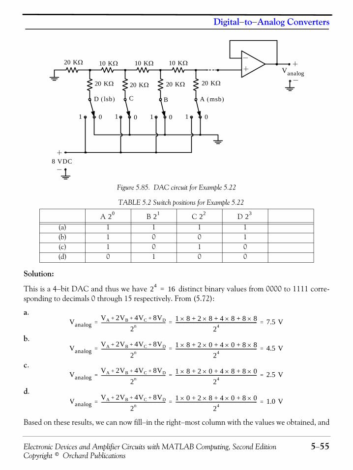
Electronic Devices and Amplifier Circuits with MATLAB Computing, Second Edition 5−55Copyright © Orchard Publications
Digital−to−Analog Converters
Figure 5.85. DAC circuit for Example 5.22
Solution:
This is a 4−bit DAC and thus we have distinct binary values from 0000 to 1111 corre-sponding to decimals 0 through 15 respectively. From (5.72):
a.
b.
c.
d.
Based on these results, we can now fill−in the right−most column with the values we obtained, and
TABLE 5.2 Switch positions for Example 5.22
A B C D (a) 1 1 1 1(b) 1 0 0 1(c) 1 0 1 0(d) 0 1 0 0
20 KΩ
20 KΩ 20 KΩ 20 KΩ 20 KΩ
10 KΩ 10 KΩ 10 KΩ
8 VDC
1 1 1 10 0 0 0
A msb( )D lsb( ) C B
Vanalog
20 21 22 23
24 16=
VanalogVA 2VB 4VC 8VD+ + +
2n------------------------------------------------------------------ 1 8× 2 8× 4 8× 8 8×+ + +
24-------------------------------------------------------------------- 7.5 V= = =
VanalogVA 2VB 4VC 8VD+ + +
2n------------------------------------------------------------------ 1 8× 2 0× 4 0× 8 8×+ + +
24-------------------------------------------------------------------- 4.5 V= = =
VanalogVA 2VB 4VC 8VD+ + +
2n------------------------------------------------------------------ 1 8× 2 0× 4 8× 8 0×+ + +
24-------------------------------------------------------------------- 2.5 V= = =
VanalogVA 2VB 4VC 8VD+ + +
2n------------------------------------------------------------------ 1 0× 2 8× 4 0× 8 0×+ + +
24-------------------------------------------------------------------- 1.0 V= = =
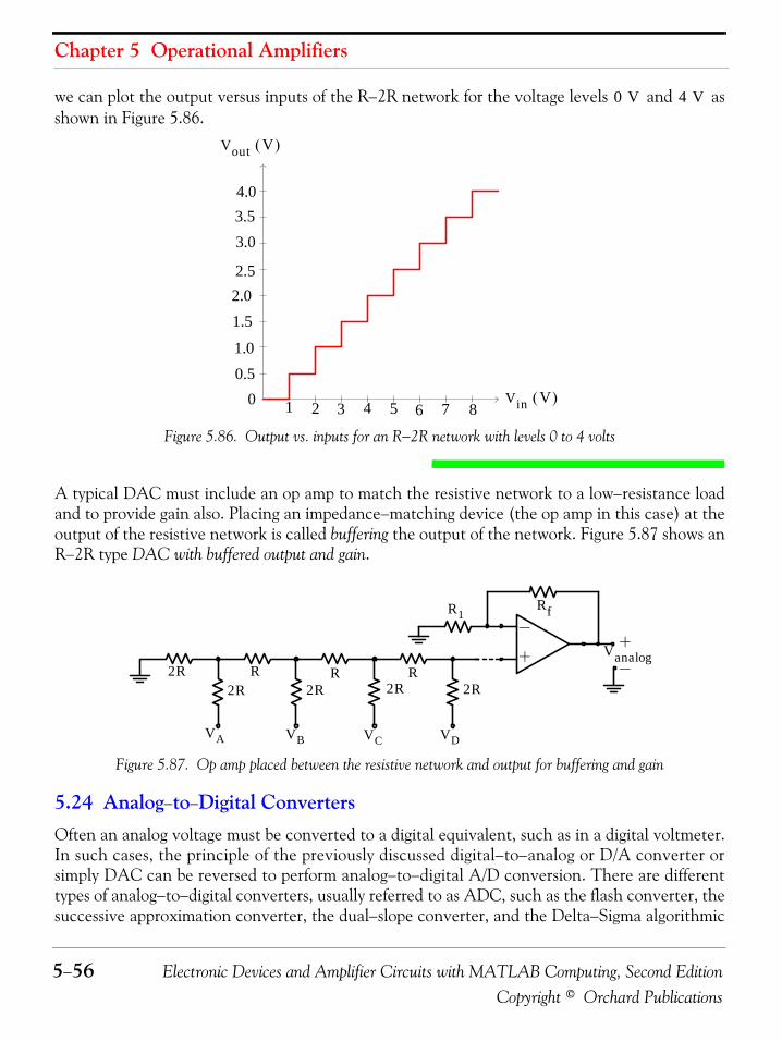
Chapter 5 Operational Amplifiers
5−56 Electronic Devices and Amplifier Circuits with MATLAB Computing, Second EditionCopyright © Orchard Publications
we can plot the output versus inputs of the R−2R network for the voltage levels and asshown in Figure 5.86.
Figure 5.86. Output vs. inputs for an R−2R network with levels 0 to 4 volts
A typical DAC must include an op amp to match the resistive network to a low−resistance loadand to provide gain also. Placing an impedance−matching device (the op amp in this case) at theoutput of the resistive network is called buffering the output of the network. Figure 5.87 shows anR−2R type DAC with buffered output and gain.
Figure 5.87. Op amp placed between the resistive network and output for buffering and gain
5.24 Analog−to−Digital ConvertersOften an analog voltage must be converted to a digital equivalent, such as in a digital voltmeter.In such cases, the principle of the previously discussed digital−to−analog or D/A converter orsimply DAC can be reversed to perform analog−to−digital A/D conversion. There are differenttypes of analog−to−digital converters, usually referred to as ADC, such as the flash converter, thesuccessive approximation converter, the dual−slope converter, and the Delta−Sigma algorithmic
0 V 4 V
876543210
1.00.5
4.03.53.0
2.52.01.5
Vout V( )
Vin V( )
2R2R
R R R2R 2R 2R
Rf
Vanalog
R1
VA VB VC VD
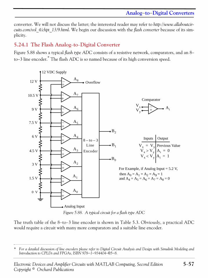
Electronic Devices and Amplifier Circuits with MATLAB Computing, Second Edition 5−57Copyright © Orchard Publications
Analog−to−Digital Converters
converter. We will not discuss the latter; the interested reader may refer to http://www.allaboutcir-cuits.com/vol_4/chpt_13/9.html. We begin our discussion with the flash converter because of its sim-plicity.
5.24.1 The Flash Analog−to−Digital ConverterFigure 5.88 shows a typical flash type ADC consists of a resistive network, comparators, and an 8−
to−3 line encoder.* The flash ADC is so named because of its high conversion speed.
Figure 5.88. A typical circuit for a flash type ADC
The truth table of the 8−to−3 line encoder is shown in Table 5.3. Obviously, a practical ADCwould require a circuit with many more comparators and a suitable line encoder.
* For a detailed discussion of line encoders please refer to Digital Circuit Analysis and Design with Simulink Modeling andIntroduction to CPLDs and FPGAs, ISBN 978−1−934404−05−8.
Overflow
Analog Input
12 V
10.5 V
9 V
7.5 V
3 V
4.5 V
6 V
1.5 V
0 V
Inputs Output
Comparator
For Example, if Analog Input = 5.2 V, then A0 = A1 = A2 = A3 = 1and A4 = A5 = A6 = A7 = A8 = 0
Previous Value8 to– 3–
EncoderLine
A2
A3
A4
A5
A6
A7
A8
A1
A0
12 VDC Supply
Vy
Vx Ai
B2
B0
B1 Vx Vy=Vx Vy> Ai 0=Vx Vy< Ai 1=
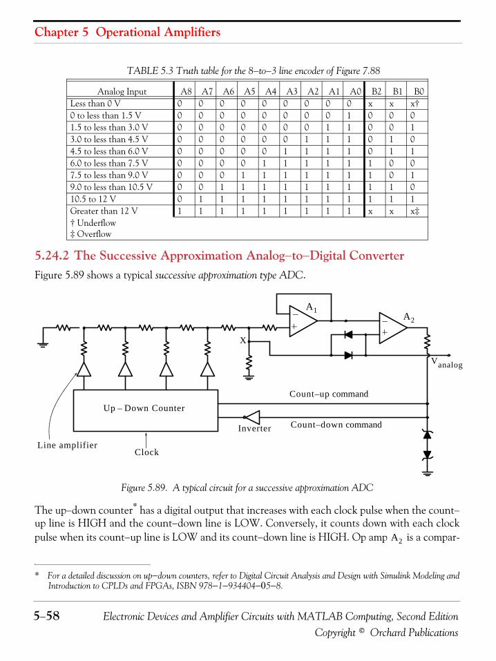
Chapter 5 Operational Amplifiers
5−58 Electronic Devices and Amplifier Circuits with MATLAB Computing, Second EditionCopyright © Orchard Publications
5.24.2 The Successive Approximation Analog−to−Digital ConverterFigure 5.89 shows a typical successive approximation type ADC.
Figure 5.89. A typical circuit for a successive approximation ADC
The up−down counter* has a digital output that increases with each clock pulse when the count−up line is HIGH and the count−down line is LOW. Conversely, it counts down with each clockpulse when its count−up line is LOW and its count−down line is HIGH. Op amp is a compar-
TABLE 5.3 Truth table for the 8−to−3 line encoder of Figure 7.88
Analog Input A8 A7 A6 A5 A4 A3 A2 A1 A0 B2 B1 B0Less than 0 V 0 0 0 0 0 0 0 0 0 x x x†0 to less than 1.5 V 0 0 0 0 0 0 0 0 1 0 0 01.5 to less than 3.0 V 0 0 0 0 0 0 0 1 1 0 0 13.0 to less than 4.5 V 0 0 0 0 0 0 1 1 1 0 1 04.5 to less than 6.0 V 0 0 0 0 0 1 1 1 1 0 1 16.0 to less than 7.5 V 0 0 0 0 1 1 1 1 1 1 0 07.5 to less than 9.0 V 0 0 0 1 1 1 1 1 1 1 0 19.0 to less than 10.5 V 0 0 1 1 1 1 1 1 1 1 1 010.5 to 12 V 0 1 1 1 1 1 1 1 1 1 1 1Greater than 12 V 1 1 1 1 1 1 1 1 1 x x x‡† Underflow‡ Overflow
* For a detailed discussion on up−down counters, refer to Digital Circuit Analysis and Design with Simulink Modeling andIntroduction to CPLDs and FPGAs, ISBN 978−1−934404−05−8.
Up Down Counter–
Line amplifier
A2
Inverter
A1
Count up command–
Count down command–
Clock
X
Vanalog
A2

Electronic Devices and Amplifier Circuits with MATLAB Computing, Second Edition 5−59Copyright © Orchard Publications
Analog−to−Digital Converters
ator and its output goes HIGH when its inverting input becomes slightly more negative than itsnon−inverting input. Conversely, its output goes LOW when its inverting input I becomes slightlymore positive than its non−inverting input. When its output is HIGH (positively saturated), thecount−up line is also HIGH. Likewise, when the output of is LOW (negatively saturated), thecount−up line is LOW also. Thus, depending on whether the output of is HIGH or LOW, theup−down counter counts digitally up or down, respectively.
When the up−down counter is counting up, an upward staircase voltage appears at point X. Whenthe counter is counting downward, a downward staircase is present at point X.
Op amp serves as a voltage follower and it buffers the DAC resistive network.The output volt-age of the resistive network is applied to the non−inverting input of and subsequently toinverting input of and it is compared with the analog input voltage which is the volt-
age to be digitized. If exceeds the voltage of the resistive network, the output of goesHIGH, and the up−down counter counts up, bringing the resistive network’s output voltage up, insteps, to the analog input . But if is less than the resistive network’s output volt-
age the output of goes LOW, and the up−down counter counts down, bringing the voltages atthe input of the comparator in line with each other.
Because this system has feedback which keeps the voltage output of the resistive network approx-imately equal to the analog input voltage , this ADC is also known as the feedback−typeADC. In this way the output of the up−down counter is always a digital equivalent of the analoginput . In a typical ADC of this type, the output of the counter is fed to a circuit to providea digital readout.
The line amplifiers are required just in case the maximum value of exceeds the level ofoutput voltages of the up−down counter. The junction diodes prevent excessive differential inputsto the comparator, and the Zener diodes are selected to clip the comparator’s output to levelscompatible with the up−down counter.
5.24.3 The Dual−Slope Analog−to−Digital ConverterThe dual−slope ADC is designed with an integrating dual−slope architecture. The simplest formof an integrating ADC uses a single−slope architecture as shown in Figure 5.90(a) where anunknown input DC voltage is integrated and the value is compared with a known reference
value .It has the advantage of providing a straightforward approach to converting a low band-width analog signal into its digital representation.
Op amp is a Miller integrator and we recall that charging a capacitor with a constant currentproduces a linear voltage across it. As shown in Figure 5.90(b), the time it takes for the integratorto cause the comparator to change state is proportional to the input voltage .
A2
A2
A1
A1
A2 Vanalog
Vanalog A2
Vanalog Vanalog
A2
Vanalog
Vanalog
Vanalog
vin
vref
A1
vin

Chapter 5 Operational Amplifiers
5−60 Electronic Devices and Amplifier Circuits with MATLAB Computing, Second EditionCopyright © Orchard Publications
Figure 5.90. An ADC with single−slope architecture
The output voltage is fed to a logic circuit which initiates counting in a binary counter.Thus, the circuitry of the this ADC translates a voltage level into a time measurement which canbe counted with the binary counter.
The single−slope converter of Figure 5.90(a) is not practical because it is subject to errors causedby variation of the timing components R and C, temperature, and aging. These errors will changethe conversion results and make measurement repeatability difficult to attain. To overcomethese sensitivities, the dual−slope integrating architecture is used. Figure 5.91 shows a typicaldual−slope ADC.
Figure 5.91. An ADC with dual−slope architecture
In the circuit of Figure 5.91(a) Switch is used to discharge the capacitor before the start of theconversion cycle and thus . The conversion cycle begins with opening Switch and
placing Switch to the position. A constant current whose value is charges the
capacitor for a reference time as shown in Figure 5.91(b). The output voltage is fed to alogic circuit which initiates counting in a binary counter. The binary counter counts the pulsesfrom a fixed clock frequency and the counting is proportional to time . At the end of time
the binary counter is reset to zero and Switch is placed to the position where hasa negative value. The current into the integrator reverses direction and its value is
vout
vin vint
vref
R
C
ttint
vref
a( ) b( )
vint
vout
S1
S2
vinvref
R Cvint
vout
vmax
a( ) b( )
tT1 T2
S1
vint 0= S1
S2 vin IN vin R⁄=
T1 vout
fC T1
T1 S2 vref vref
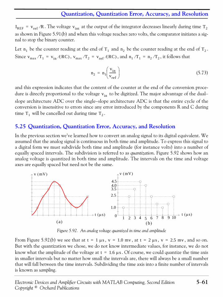
Electronic Devices and Amplifier Circuits with MATLAB Computing, Second Edition 5−61Copyright © Orchard Publications
Quantization, Quantization Error, Accuracy, and Resolution
. The voltage at the output of the integrator decreases linearly during time as shown in Figure 5.91(b) and when this voltage reaches zero volts, the comparator initiates a sig-nal to stop the binary counter.
Let be the counter reading at the end of and be the counter reading at the end of .Since , , and , it follows that
(5.73)
and this expression indicates that the content of the counter at the end of the conversion proce-dure is directly proportional to the voltage to be digitized. The major advantage of the dual−slope architecture ADC over the single−slope architecture ADC is that the entire cycle of theconversion is insensitive to errors since any error introduced by the components R and C duringtime will be cancelled out during time .
5.25 Quantization, Quantization Error, Accuracy, and ResolutionIn the previous section we’ve learned how to convert an analog signal to its digital equivalent. Weassumed that the analog signal is continuous in both time and amplitude. To express this signal toa digital form we must subdivide both time and amplitude (for instance volts) into a number ofequally spaced intervals. The subdivision is referred to as quantization. Figure 5.92 shows how ananalog voltage is quantized in both time and amplitude. The intervals on the time and voltageaxes are equally spaced but need not be the same.
Figure 5.92. An analog voltage quantized in time and amplitude
From Figure 5.92(b) we see that at , , at , , and so on.But with the quantization we chose, we do not know intermediate values, for instance, we do notknow what the amplitude of the voltage at . Of course, we could quantize the time axisin smaller intervals but no matter how small the intervals are, there will always be a small numberthat will fall between the time intervals. Subdividing the time axis into a finite number of intervalsis known as sampling.
IREF vref R⁄= vint T2
n1 T1 n2 T2
vmax T1⁄ vin RC( )⁄= vmax T2⁄ vref RC( )⁄= n1 T1⁄ n2 T2⁄=
n2 n1vinvref---------
⎝ ⎠⎜ ⎟⎛ ⎞
=
vin
T1 T2
6510 2 3 9 104 7 8
v mV( )
t μs( )
1.0
2.53.54.04.5
v mV( )
t μs( )
a( ) b( )
t 1 μs= v 1.0 mv= t 2 μs= v 2.5 mv=
t 1.6 μs=

Chapter 5 Operational Amplifiers
5−62 Electronic Devices and Amplifier Circuits with MATLAB Computing, Second EditionCopyright © Orchard Publications
We may wonder what sampling rate one must choose to faithfully (exactly) reproduce an analogsignal such as that of Figure 5.92(a) from its digital equivalent of Figure 5.92(b). The answer tothis question is provided by the well known sampling theorem which states that to faithfully repro-duce an analog signal from it digital equivalent, the analog signal, before conversion to a digital,must be sampled at least twice the frequency of the highest frequency component of the signal.This minimum frequency is known as the Nyquist rate. Thus, to reproduce exactly a 10 KHz sinu-soid, theoretically, we must sample it at least at 20 KHz rate and in this case the Nyquist rate is20 KHz. And how do we know the highest frequency component of a signal? The answer is fromFourier* series.
In practice, the Nyquist rate is not sufficient; it is a theoretical value and because of electronicequipment limitations and component imperfections, this theoretical value cannot be achieved.A general rule is to sample at five to ten times the highest frequency of the analog signal.
The difference between an exact analog value and the closest discrete value after sampling isknown as quantization error. Obviously, every ADC suffers from a quantization error no matterhow small.
The linearity of an ADC or DAC is a measure of accuracy and it is an indication of how close theconverter’s output is to the ideal input−output transfer characteristics. The output of an ADC isaccurate to within of the least significant bit (LSD).
Example 5.23
What is the accuracy of an 8−bit ADC if the converter encodes an analog voltage between 0 and+15 volts.Solution:
The LSD represents increments of so the LSD is . With an accu-racy of of the LSD, this ADC produces a digital output that represents the analog inputwithin .
Another term used in ADCs and DACs is resolution. Accuracy and resolution have differentmeaning. Accuracy is the degree with which an instrument measures a variable in terms of anaccepted standard value or true value; usually measured in terms of inaccuracy but expressed asaccuracy; often expressed as a percentage of full−scale range. Resolution is the smallest change inthe parameter being measured that causes a detectable change in the output of the instrument.Typically, an eight, ten, or at most twelve bits of digital output provides adequate resolution.
* For a thorough discussion on Fourier series and the Fourier transform, please refer to Signals and Systems with MAT-LAB Computing and Simulink Modeling, Fourth Edition, ISBN 978−1−934404−11−9.
1 2⁄±
16 28⁄ 16 256⁄ 1 16⁄= = 1 16⁄1 2⁄±1 32⁄± 31.3 mV=
Electronic Devices and Amplifier Circuits with MATLAB Computing, Second Edition 5−63Copyright © Orchard Publications
Op Amps in Analog Computers
For example, a voltmeter is said to have a resolution may be . This means that this valueis the step size of the voltmeter’s measuring capability. In other words, it is the value with only onedecimal place which can be measured and possibly recorded against other voltage records as thevoltmeter is not able to detect any smaller step size in voltage changes. By comparison, the accu-racy of, say refers to the degree to which this value may differ from the true value.
Example 5.24
How many clock cycles would we need to obtain a 10−bit resolution with a dual−slope ADC?Solution:
The integration time would require clock cycles and also another
clock cycles for integration time for a maximum conversion of clock cycles.
5.26 Op Amps in Analog Computers
Present day analog computers are build with op amps. In an analog computer the numbers repre-senting the variables are voltages. We will not discuss analog computers in this section. We willsimply present two simple examples to illustrate how op amps are used in analog computation.
Example 5.25
Using two op amps and resistors, design an analog computer that will solve the equations
(5.74)
where , , , , , and are constant coefficients.
Solution:
We observe that the arithmetic operations involved in (5.74) are addition and multiplication byconstant coefficients. The two additions can be performed by summing op amps. Multiplication bya coefficient greater than unity can be performed with an op amp with feedback, and if the coeffi-cient is less than unity, we can use a voltage divider. It is convenient to express the given equa-tions as
(5.75)
0.1 mV
0.2 mV
T1 210 1024= 210 1024=
T2 2 210× 2048=
a1x b1y+ c1=
a2x b2y+ c2=
a1 a2 b1 b2 c1 c2
xc1a1-----
b1a1-----y–=
yc2b2-----
a2b2-----x–=

Chapter 5 Operational Amplifiers
5−64 Electronic Devices and Amplifier Circuits with MATLAB Computing, Second EditionCopyright © Orchard Publications
and these equations can be solved using two summing amplifiers as shown in Figure 5.93. Asshown in Figure 5.93, the output of op amp is a voltage representing the unknown and theoutput of op amp is a voltage representing the unknown . The fraction of isobtained from the potentiometer and this is summed in op amp with the fraction
obtained from potentiometer and voltage source . A similar summation isobtained by amplifier .
Figure 5.93. Analog computer for the solution of two simultaneous equations with two unknowns
In Figure 5.93 the scaling factors chosen must ensure that the voltages representing theunknowns do not exceed the output capability of the op amps. This procedure can be extendedto the solution of simultaneous equations with more than two unknowns.
Before we consider the next example for a circuit to solve a simple differential equation, we needto discuss a practical integrator circuit that provides some means of setting a desired initial valueat the beginning of the integration cycle. It is also necessary to provide means to stop the integra-tor at any time, and for the integrator output to remain constant at the value it has reached atthat time. An integrator circuit that provides these means is shown in Figure 5.94.
Initially, the integrator sets the initial condition with the switches as shown in Figure 5.94(a),and denoting the initial condition as . The voltage across the capacitor cannot change instan-taneously, and thus
A1 x
A2 y b1 a1⁄ y
R adj4 A1
c1– a1⁄ R adj1 VS1
A2
VS1
VS2
R1
R2
R3
R4
R f1
R f2
R adj1
R adj2
R adj4
R adj3
x
c2 b2⁄–y
c1 a1⁄–
a2 b2⁄( )x
b1 a1⁄( )y
A1
A2
V0

Electronic Devices and Amplifier Circuits with MATLAB Computing, Second Edition 5−65Copyright © Orchard Publications
Op Amps in Analog Computers
(5.76)
Figure 5.94. Integrator circuit mode control
When switched to the compute mode, the circuit integrates the input voltage and the value of theoutput voltage is
(5.77)
The integrator is then switched to the hold mode and remains constant at the value reached atthe end of the compute mode. We observe that the switches in the hold mode are positioned as inthe set initial condition mode.
Example 5.26
Using one op amp, resistors, capacitors, and switches design an analog computer that will solvethe simple differential equation
(5.78)
vout t 0=( )R2R1------– V0=
R1
R1
a( ) Set Initial Condition Mode
R1
R2
R2R2
Rin
RinRin
vin
vinvin
VS
VSVS
S1
S1
S1
S2
S2S2
CC
C
b( ) Compute Mode
c( ) Hold Mode
vout
vout
vout
vout vout t 0=( ) 1RinC------------ vin td
0
t
∫–=
dvCdt
--------- 1C----iC=

Chapter 5 Operational Amplifiers
5−66 Electronic Devices and Amplifier Circuits with MATLAB Computing, Second EditionCopyright © Orchard Publications
where C is a constant representing the value of a capacitor, is the voltage across the capaci-
tor and is the current through the capacitor and the initial condition is .
Solution:
The given differential equation can be solved with the circuit of Figure 5.95.
Figure 5.95. Integrator circuit for Example 5.26
Initially, a voltage representing the value of is applied to the integrator and the output ofthe integrator will be a voltage representing . Then, the output is multiplied by and fedback to the input.
dvC
iC vC t 0–( ) V0=
iC
1C----iC
Rin
R2R1
S1
V0
VS
C
S2
dvC dt⁄
iC 1 C⁄
Electronic Devices and Amplifier Circuits with MATLAB Computing, Second Edition 5−67Copyright © Orchard Publications
Summary
5.27 Summary• The operational amplifier (op amp) is the most versatile amplifier and its main features are:
1. Very high input impedance (resistance)
2. Very low output impedance (resistance)
3. Capable of producing a very large gain that can be set to any value by connection of externalresistors of appropriate values
4. Frequency response from DC to frequencies in the MHz range
5. Very good stability
6. Operation to be performed, i.e., addition, integration etc. is done externally with proper selec-tion of passive devices such as resistors, capacitors, diodes, and so on.
• The gain of an inverting op amp is the ratio where is the feedback resistor whichallows portion of the output to be fed back to the minus (−) input. The minus (−) sign impliesthat the output signal has opposite polarity from that of the input signal.
• The gain of an non−inverting op amp is where is the feedback resistor whichallows portion of the output to be fed back to the minus (−) input which is grounded throughthe resistor. The output signal has the same polarity from that of the input signal.
• In a unity gain op amp the output is the same as the input. A unity gain op amp is used to pro-vide a very high resistance between a voltage source and the load connected to it.
• Op amps are also used as active filters.
• The input resistance is defined as the ratio of the applied voltage to the current
drawn by the circuit, that is, .
• The output resistance is the ratio of the open circuit voltage to the short circuit current,
that is, .
• Operational amplifiers can operate either a closed−loop or an open−loop configuration. Theoperation, closed−loop or open−loop, is determined by whether or not feedback is used. Mostoperational amplifiers operate in the closed−loop configurations, that is, with feedback.
• The gain of any amplifier varies with frequency. The specification sheets for operational ampli-fiers state the open−loop at DC or . At higher frequencies, the gain is much lower anddecreases as frequency increases at the rate of .
• The unity gain frequency, is the frequency at which the gain is unity.
• The gain−bandwidth product is an important op amp parameter and is related to the unity gain
Rf Rin⁄– Rf
1 Rf Rin⁄+ Rf
Rin
Rin vS iS
Rin vS iS⁄=
Rout
Rout vOC iSC⁄=
0 Hz20 dB decade⁄–

Chapter 5 Operational Amplifiers
5−68 Electronic Devices and Amplifier Circuits with MATLAB Computing, Second EditionCopyright © Orchard Publications
frequency as .
• The use of negative feedback increases the bandwidth of an operational amplifier circuit butdecreases the gain so that the gain times bandwidth product is always equal to the unity gainfrequency of the op amp.
• Common−mode rejection refers to the condition that if the inputs to the op amp are exactlythe same, i.e., if , then . In other words, the op amp rejects any signals atits inputs that are the same.
• The transresistance gain is defined as the ratio .
• The closed loop transfer function is defined as and in the invert-ing input mode .
• The output voltage of an op amp integrator is the integral of the input voltage.
• The output voltage of an op amp differentiator is the first derivative of the input voltage.
• A summing amplifier in the inverting mode produces the negative sum of any number of inputvoltages. Likewise, a summing amplifier in the non−inverting mode produces the positive sumof any number of input voltages.
• A differential input op amp allows input signals to be applied simultaneously to both input ter-minals and produce an output of the difference between the input signals. A differential inputamplifier must have a high common mode rejection ratio (CMRR) defined as
where the differential gain is the gain with the input signals applied differentially, and com-mon mode gain is the ratio of the output common−mode voltage to the input com-mon−mode voltage , that is, . Ideally, is zero but in reality isfinite and much smaller than unity.
• High input resistance differential input amplifiers are suitable for use in differential measure-ment applications and the associated circuits are referred to as instrumentation amplifiers.
• General purpose op amps are normally internally frequency compensated so that they will bestable with all values of resistive feedback. Other types of op amps are without internal fre-quency compensation and require external connection of frequency compensating componentsto the op amp. Typically, the compensating components alter the open loop gain characteris-tics so that the roll−off is about over a wide range of frequencies.
• The slew rate (SR) is defined as the maximum rate of change of an output voltage produced in
Gain Bandwidth× Unity Gain Frequency=
vin2 vin1= vout 0=
vout iin⁄
G s( ) G s( ) Vout s( ) Vin s( )⁄=
G s( ) Zf s( ) Z1 s( )⁄–=
CMRR Differential gainCommon mode gain------------------------------------------------------
AdAcm----------= =
Av
Vcm out
Vcm in Acm Vcm out Vcm in⁄= Acm
20 dB decade⁄

Electronic Devices and Amplifier Circuits with MATLAB Computing, Second Edition 5−69Copyright © Orchard Publications
Summary
response to a large input step function and it is normally expressed in volts per microsecond,that is,
• Op amps can also be used in circuits with non−linear devices. We have introduced the positiveand negative voltage limiters, half−wave rectifier with limited positive or negative output.
• A comparator is a circuit that senses changes in a varying signal and produces an output when athreshold value is reached. As a comparator, an op amp is used without feedback, that is, the opamp is used in the open loop configuration.
• A Wien bridge oscillator produces a sinusoidal output. This oscillator uses two RC networksconnected to the non−inverting input of the op amp to form a frequency selective feedback cir-cuit and this causes oscillations to occur. It also amplifies the signal with two negative feedbackresistors.
• A digital−to−analog converter (D/A converter or DAC) is used to convert a binary output froma digital system to an equivalent analog voltage. If there are 16 combinations of the voltages through , the analog device should have 16 possible values.
• A DAC with binary−weighted resistors has the disadvantage that it requires a large number ofprecision resistors.
• A DAC formed with an R−2R ladder network, requires more resistors, but only two sets of pre-cision resistance values, R and 2R.
• A DAC must include an op amp to match the resistive network to a low−resistance load and toprovide gain also. Placing an impedance−matching device (the op amp in this case) at the out-put of the resistive network is called buffering the output of the network.
• An analog−to−digital converter (A/D converter or ADC) converts an analog signal to its binaryequivalent. Popular types of ADCs are the flash converter, the successive approximation, andthe dual−slope.
• Quantization is the process where an analog signal is subdivided into small discrete time andamplitude intervals. Subdividing the time axis into a finite number of intervals is known assampling. The difference between an exact analog value and the closest discrete value aftersampling is known as quantization error.
• The sampling theorem states that to faithfully reproduce an analog signal from it digital equiv-alent, the analog signal, before conversion to a digital, must be sampled at least twice the fre-quency of the highest frequency component of the signal. This minimum frequency is known asthe Nyquist rate. The Nyquist rate is not sufficient; because of electronic equipment limitationsand component imperfections, this theoretical value cannot be achieved. A general rule is tosample at five to ten times the highest frequency of the analog signal.
SlewRate SRdvoutdtmax-------------= =
VD
VA
Chapter 5 Operational Amplifiers
5−70 Electronic Devices and Amplifier Circuits with MATLAB Computing, Second EditionCopyright © Orchard Publications
• The linearity of an ADC or DAC is a measure of accuracy and it is an indication of how closethe converter’s output is to the ideal input−output transfer characteristics. The output of anADC is accurate to within of the least significant bit (LSD).
• Accuracy is the degree with which an instrument measures a variable in terms of an acceptedstandard value or true value.
• Resolution is the smallest change in the parameter being measured that causes a detectablechange in the output of the instrument. Typically, an eight, ten, or at most twelve bits of digi-tal output provides adequate resolution.
• Present day analog computers are build with op amps. In an analog computer the numbersrepresenting the variables are voltages.
1 2⁄±
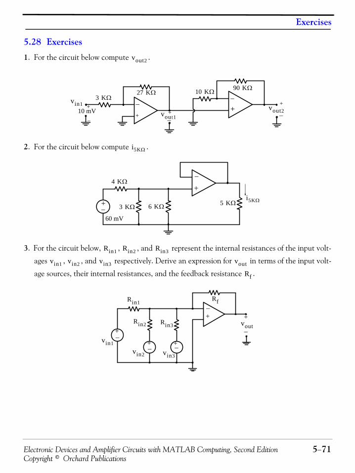
Electronic Devices and Amplifier Circuits with MATLAB Computing, Second Edition 5−71Copyright © Orchard Publications
Exercises
5.28 Exercises
1. For the circuit below compute .
2. For the circuit below compute .
3. For the circuit below, , , and represent the internal resistances of the input volt-
ages , , and respectively. Derive an expression for in terms of the input volt-
age sources, their internal resistances, and the feedback resistance .
vout2
+
−10 mV
+
−−+ +
−
−
+vout2
3 KΩ27 KΩ 10 KΩ 90 KΩ
vout1
vin1
i5KΩ
60 mV
+
−
3 KΩi5KΩ
4 KΩ
6 KΩ 5 KΩ+−
Rin1 Rin2 Rin3
vin1 vin2 vin3 vout
Rf
vin1
vin2 vin3
Rin1
Rin2 Rin3
−−
−
−
−
++
++
+
Rf
vout

Chapter 5 Operational Amplifiers
5−72 Electronic Devices and Amplifier Circuits with MATLAB Computing, Second EditionCopyright © Orchard Publications
4. For the circuit below compute .
5. The op−amp circuit (a) below can be represented by its equivalent circuit (b). For the circuit(c), compute the value of so that it will receive maximum power.
6. For the circuit below compute using Thevenin’s theorem.
vout
40 mV
+
−vout
10 KΩ
20 KΩ40 KΩ
50 KΩ
+
+−
−
Rload
+
−+
−− +
+−
−
+
(a)(b)
R1Rf R1
RfR1------vinvin
vin
vout
vout
+
−
(c)
vin+
−
2 KΩ 20 KΩ
+
− 5 KΩ
15 KΩRload
vout
+
−
v5KΩ
+−
−
+
+
−
vout
72 mV
v5KΩ 20 KΩ
12 KΩ
84 KΩ
100 KΩ
5 KΩ
4 KΩ
+−

Electronic Devices and Amplifier Circuits with MATLAB Computing, Second Edition 5−73Copyright © Orchard Publications
Exercises
7. For the circuit below compute the gain .
8. For the circuit below show that the gain is given by
9. The specifications for the popular 741 op amp state that the open−loop gain is and theunity gain frequency is . Plot the frequency response for open−loop gain versus fre-quency curve and the closed−loop frequency response for a gain of .
10. For the op amp shown below the open−loop gain is .
a. Find if and
b. Find if and
c. Find if and
Gv vout vin⁄=
++
−− voutvin
R2R1
R3R4
R5
200 KΩ
40 KΩ
50 KΩ
50 KΩ
40 KΩ
+
Gvvoutvin---------- 1
R1------– R4 R2
R4R3------ 1+⎝ ⎠
⎛ ⎞+= =
++
−
voutvin
R1
R2R3 R4
+
200 000,1 MHz
10
100 000,
vout
vin1
vin2
vin1 vin2 3 mV= vout 5 V=
vin2 vin1 2 mV= vout 5– V=
vout vin1 2 mV= vin2 3– mV=
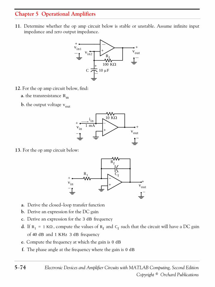
Chapter 5 Operational Amplifiers
5−74 Electronic Devices and Amplifier Circuits with MATLAB Computing, Second EditionCopyright © Orchard Publications
11. Determine whether the op amp circuit below is stable or unstable. Assume infinite inputimpedance and zero output impedance.
12. For the op amp circuit below, find:a. the transresistance
b. the output voltage
13. For the op amp circuit below:
a. Derive the closed−loop transfer functionb. Derive an expression for the DC gainc. Derive an expression for the frequency
d. If , compute the values of and such that the circuit will have a DC gain
of and frequency
e. Compute the frequency at which the gain is
f. The phase angle at the frequency where the gain is
voutvin1
vin2
+
C 10 μF
Rf
100 KΩ+
+
+
Rm
vout
−+
10 KΩ
voutvin
1 mA+
+
−−
iin
−R1
Rf
vin−
−
Cf
vout+
+
+
3 dB
R1 1 KΩ= Rf Cf
40 dB 1 KHz 3 dB
0 dB
0 dB
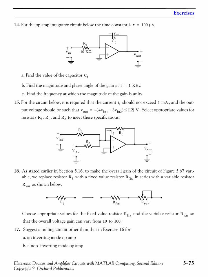
Electronic Devices and Amplifier Circuits with MATLAB Computing, Second Edition 5−75Copyright © Orchard Publications
Exercises
14. For the op amp integrator circuit below the time constant is .
a. Find the value of the capacitor
b. Find the magnitude and phase angle of the gain at
c. Find the frequency at which the magnitude of the gain is unity
15. For the circuit below, it is required that the current should not exceed , and the out-
put voltage should be such that . Select appropriate values for
resistors , , and to meet these specifications.
16. As stated earlier in Section 5.16, to make the overall gain of the circuit of Figure 5.67 vari-able, we replace resistor with a fixed value resistor in series with a variable resistor
as shown below.
Choose appropriate values for the fixed value resistor and the variable resistor so
that the overall voltage gain can vary from to .
17. Suggest a nulling circuit other than that in Exercise 16 for:
a. an inverting mode op amp
b. a non−inverting mode op amp
τ 100 μs=
vin vout10 KΩ
CfR1
Cf
f 1 KHz=
if 1 mA
vout 4vin1 3vin2+( ) 12 V≤–=
Rf R1 R2
Rfvin1
+
−
−
+vout
R1
R2+
−vin2
if
+−
R1 Rfix
Rvar
RfixR1 Rvar
Rfix Rvar
10 100
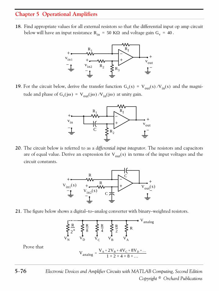
Chapter 5 Operational Amplifiers
5−76 Electronic Devices and Amplifier Circuits with MATLAB Computing, Second EditionCopyright © Orchard Publications
18. Find appropriate values for all external resistors so that the differential input op amp circuitbelow will have an input resistance and voltage gain .
19. For the circuit below, derive the transfer function and the magni-
tude and phase of at unity gain.
20. The circuit below is referred to as a differential input integrator. The resistors and capacitorsare of equal value. Derive an expression for in terms of the input voltages and thecircuit constants.
21. The figure below shows a digital−to−analog converter with binary−weighted resistors.
Prove that
Rin 50 KΩ= Gv 40=
Rf
vin1 vout
R1
R2
+
−vin2 R3
+++
−
−
−
Gv s( ) Vout s( ) Vin s( )⁄=
Gv jω( ) Vout jω( ) Vin jω( )⁄=
Rf
vin vout
R1
R2−C
++
+ −
−
Vout s( )
Vin1 s( ) +
−−
+Vout s( )
R
R+
− Vin2 s( )
C
C
+−
Vanalog
VBVCVD VAVN
RR2----R
4----R
8----R
2 n------
VanalogVA 2VB 4VC 8VD …+ + + +
1 2 4 8 …+ + + +------------------------------------------------------------------------------=
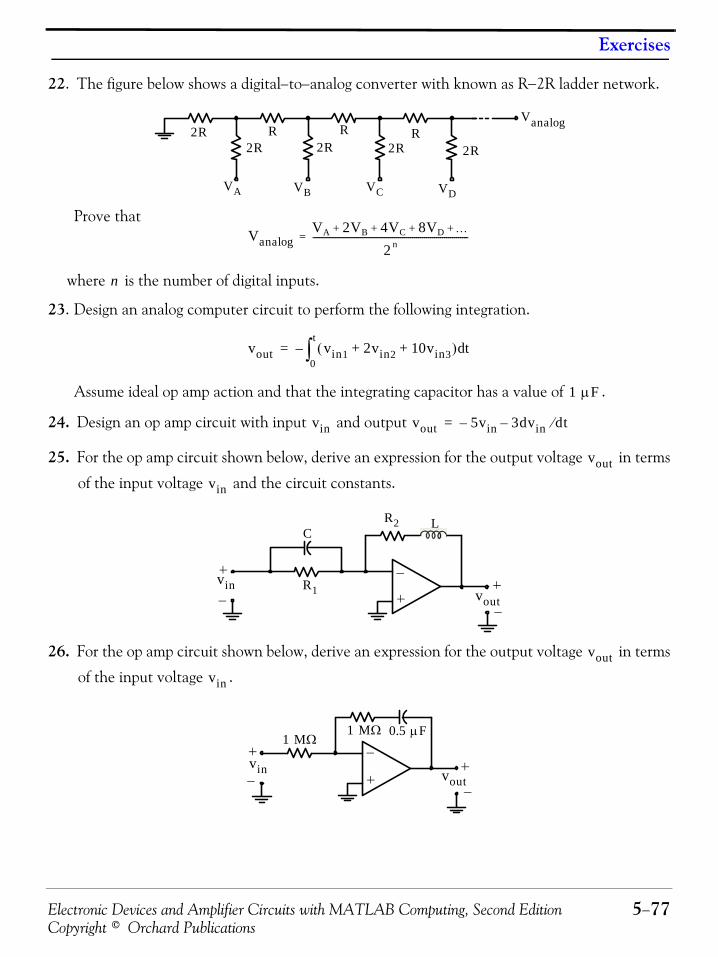
Electronic Devices and Amplifier Circuits with MATLAB Computing, Second Edition 5−77Copyright © Orchard Publications
Exercises
22. The figure below shows a digital−to−analog converter with known as R−2R ladder network.
Prove that
where is the number of digital inputs.
23. Design an analog computer circuit to perform the following integration.
Assume ideal op amp action and that the integrating capacitor has a value of .
24. Design an op amp circuit with input and output
25. For the op amp circuit shown below, derive an expression for the output voltage in terms
of the input voltage and the circuit constants.
26. For the op amp circuit shown below, derive an expression for the output voltage in terms
of the input voltage .
VA VB VC VD
R R R2R2R 2R 2R 2R
Vanalog
VanalogVA 2VB 4VC 8VD …+ + + +
2 n------------------------------------------------------------------------------=
n
vout vin1 2vin2 10vin3+ +( ) td0
t
∫–=
1 μF
vin vout 5vin– 3dvin dt⁄–=
vout
vin
vin
C
R1
R2 L
vout
vout
vin
vin vout
1 MΩ1 MΩ 0.5 μF

Chapter 5 Operational Amplifiers
5−78 Electronic Devices and Amplifier Circuits with MATLAB Computing, Second EditionCopyright © Orchard Publications
5.29 Solutions to End−of−Chapter Exercises1.
and thus
Then
2. We assign , , and as shown below.
and by the voltage division expression
and since this is a unity gain amplifier, we obtain
Then
+
−10 mV
+
−−+ +
−
−
+vout2
3 KΩ27 KΩ 10 KΩ 90 KΩ
vout1
vin1
vin2+
−
vout1 27 3⁄( ) 10×– 90 mV–= =
vin2 vout1 90 mV–= =
vout2 1 9010------+⎝ ⎠
⎛ ⎞ 90–( )× 0.9 V–= =
v1 vload Rload
60 mV
+
−
3 KΩi5KΩ
4 KΩ
6 KΩ
5 KΩ
+−
+v1
−
vload Rload
+
−
3 KΩ 6 KΩ|| 2 KΩ=
v12 KΩ
4 KΩ 2 KΩ+----------------------------------- 60 mV× 20 mV= =
vload v1 20 mV= =
i5KΩvloadRload------------- 20 mV
5 KΩ----------------- 20 10 3–×
5 103×----------------------- 4 10 6– A× 4 μA= = = = =

Electronic Devices and Amplifier Circuits with MATLAB Computing, Second Edition 5−79Copyright © Orchard Publications
Solutions to End−of−Chapter Exercises
3.
By superposition
where
We observe that the minus (−) input is a virtual ground and thus there is no current flow in and . Also,
and
Then,
4. We assign voltages and as shown below. At the minus (−) terminal
vin1
vin2 vin3
Rin1
Rin2 Rin3
−−
−
−
−
++
++
+
Rf
vout
vout vout1 vout2 vout3+ +=
vout1 vin2 0=
vin3 0=
RfRin1----------vin1–=
Rin1 Rin2
vout2 vin1 0=
vin3 0=
RfRin2----------vin2–=
vout3 vin1 0=
vin2 0=
RfRin3---------- v– in3( )–=
vout Rfvin3Rin3----------
vin2Rin2----------
vin1Rin1----------––
⎝ ⎠⎜ ⎟⎛ ⎞
=
v1 v2
v1 40 mV–
10 KΩ-----------------------------
v1 vout–
50 KΩ---------------------+ 0=
650 103×--------------------v1
150 103×--------------------vout– 4 10 6–×=

Chapter 5 Operational Amplifiers
5−80 Electronic Devices and Amplifier Circuits with MATLAB Computing, Second EditionCopyright © Orchard Publications
At the plus (+) terminal
Since we equate the nodal equations and we obtain
Multiplication by yields
Check with (5.16), Page 5-22, using MATLAB:
R1=10000; R2=20000; R3=40000; Rf=50000; Vin=40*10^(−3);Vout=(R1*R3−R2*Rf)*Vin/(R1*(R2+R3))
Vout = -0.0400
5. We attach the , , and resistors to the equivalent circuit as shown below.
By Thevenin’s theorem,
40 mV
+
−vout
10 KΩ
20 KΩ40 KΩ
50 KΩ
+
+−
−
v1
v2
v2 40 mV–
20 KΩ-----------------------------
v240 KΩ-----------------+ 0=
340 10 3×---------------------v2 2 10 6–×=
v280 10 3–×
3-----------------------=
v2 v1=
650 103×-------------------- 80 10 3–×
3-----------------------⎝ ⎠
⎛ ⎞ 150 103×--------------------vout– 4 10 6–×=
50 103×
2 80 10 3–×× 50 103××
50 103×----------------------------------------------------------- vout– 4 10 6–× 50 103××=
vout 40 mV–=
5 KΩ 15 KΩ Rload
vTH vOC vab15 KΩ
5 KΩ 15 KΩ+-------------------------------------- 10vin–( )= = =

Electronic Devices and Amplifier Circuits with MATLAB Computing, Second Edition 5−81Copyright © Orchard Publications
Solutions to End−of−Chapter Exercises
or
Because the circuit contains a dependent source, we must compute the Thevenin resistanceusing the relation where is found from the circuit below.
We observe that the short circuit shorts out the and thus
Then
and the Thevenin equivalent circuit is shown below.
Therefore, for maximum power transfer we must have
+−2 KΩ
10vinvin
5 KΩ15 KΩ
×
×
b
a+− Rload
vTH 7.5vin–=
RTH vTH iSC⁄= iSC
a
+−
10vin
5 KΩ
15 KΩ
×
×
b iSC
15 KΩ
iSC10vin–
5 KΩ---------------- 2 10 3– vin×–= =
RTH7.5vin–
2 10 3– vin×–------------------------------- 3.75 KΩ= =
vTH
3.75 KΩRload+
−
RTH
Rload RTH 3.75 KΩ= =

Chapter 5 Operational Amplifiers
5−82 Electronic Devices and Amplifier Circuits with MATLAB Computing, Second EditionCopyright © Orchard Publications
6. The given circuit is a non−inverting op amp whose equivalent circuit is shown below.
For this circuit and the output is
Attaching the external resistors to the equivalent circuit above we obtain the circuit below.
To find the Thevenin equivalent at points a and b we disconnect the resistor. Whenthis is done there is no current in the resistor and the circuit simplifies to the oneshown below.
By KVL
or
Also
or
−
+
1RfRin-------+⎝ ⎠
⎛ ⎞ vinvoutvin
+
−
+−
vin v5KΩ=
vout 1RfRin--------+
⎝ ⎠⎜ ⎟⎛ ⎞
v5KΩ 1 10020
---------+⎝ ⎠⎛ ⎞ v5KΩ 6v5KΩ= = =
v5KΩ
72 mV
12 KΩ
4 KΩ
84 KΩ
5 KΩ
×
×
a
b6v5KΩ
++ +
− −−
5 KΩ4 KΩ
6v5KΩ72 mV
12 KΩ 84 KΩ
i
a
b
vab −+−
×
× −
+
+
12 KΩ 84 KΩ+( )i 6v5KΩ+ 72 mV=
i72 mV 6v5KΩ–
12 KΩ 84 KΩ+( )----------------------------------------------=
vTH vab v5KΩ 72 mV 12 KΩ( )i– 72 mV 12 KΩ72 mV 6v5KΩ–
96 KΩ---------------------------------------⎝ ⎠
⎛ ⎞–= = = =
vTH 72 mV 9 mV–34---v5KΩ+=
Electronic Devices and Amplifier Circuits with MATLAB Computing, Second Edition 5−83Copyright © Orchard Publications
Solutions to End−of−Chapter Exercises
and thus
The Thevenin resistance is found from where is computed with the termi-nals a and b shorted making and the circuit is as shown in Figure (a) below. We alsoperform voltage−source to current−source transformation and we obtain the circuit shown inFigure (b) below.
Now,
and by the current division expression
Therefore,
and the Thevenin equivalent circuit with the resistor is shown below.
Finally, by the voltage division expression
v5KΩ34---v5KΩ– 63 mV=
vTH vab v5KΩ 252 mV= = =
RTH vOC iSC⁄= iSC
v5KΩ 0=
72 mV
12 KΩ
84 KΩa
biSC
4 KΩ
6 μA
12 KΩ
84 KΩa
biSC
4 KΩ
−+
(a) (b)
12 KΩ 84 KΩ|| 10.5 KΩ=
iSC iab10.5 KΩ
10.5 KΩ 4 KΩ+------------------------------------------ 6 μA× 126
29--------- μA= = =
RTHvOCiSC--------- 252
126 29⁄------------------- 58 KΩ= = =
5 KΩ
+
− 5 KΩ
a
b
12 KΩ
vTH
+−
RTH
252 mV
v5KΩ
v5KΩ5
58 5+--------------- 252× 20 mV= =
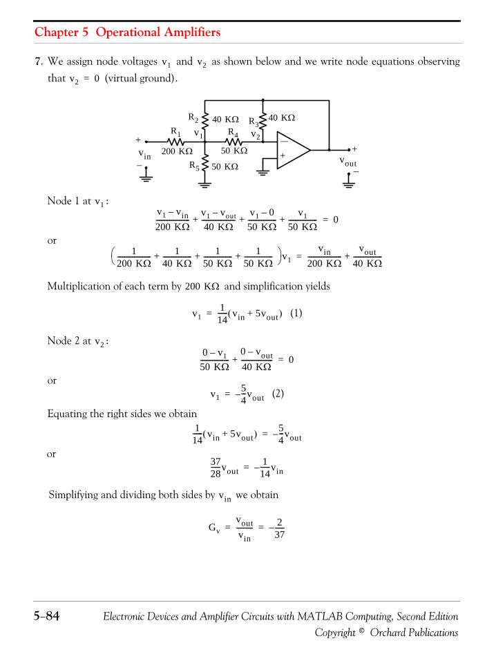
Chapter 5 Operational Amplifiers
5−84 Electronic Devices and Amplifier Circuits with MATLAB Computing, Second EditionCopyright © Orchard Publications
7. We assign node voltages and as shown below and we write node equations observingthat (virtual ground).
Node 1 at :
or
Multiplication of each term by and simplification yields
(1)
Node 2 at :
or (2)
Equating the right sides we obtain
or
Simplifying and dividing both sides by we obtain
v1 v2
v2 0=
++
−− voutvin
R2R1
R3R4
R5
200 KΩ
40 KΩ
50 KΩ
50 KΩ
40 KΩ
+
v1 v2
v1v1 vin–
200 KΩ--------------------
v1 vout–
40 KΩ--------------------
v1 0–
50 KΩ-----------------
v150 KΩ-----------------+ + + 0=
1200 KΩ-------------------- 1
40 KΩ----------------- 1
50 KΩ----------------- 1
50 KΩ-----------------+ + +⎝ ⎠
⎛ ⎞ v1vin
200 KΩ--------------------
vout40 KΩ-----------------+=
200 KΩ
v11
14------ vin 5vout+( )=
v20 v1–
50 KΩ-----------------
0 vout–
40 KΩ-------------------+ 0=
v154---vout–=
114------ vin 5vout+( ) 5
4---vout–=
3728------vout
114------vin–=
vin
Gvvoutvin---------- 2
37------–= =
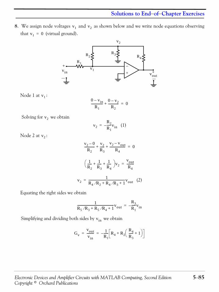
Electronic Devices and Amplifier Circuits with MATLAB Computing, Second Edition 5−85Copyright © Orchard Publications
Solutions to End−of−Chapter Exercises
8. We assign node voltages and as shown below and we write node equations observingthat (virtual ground).
Node 1 at :
Solving for we obtain
(1)
Node 2 at :
(2)
Equating the right sides we obtain
Simplifying and dividing both sides by we obtain
v1 v2
v1 0=
++
−
voutvin
R1
R2R3 R4
+ v1
v2
v10 vin–
R1----------------
0 v2–
R2--------------+ 0=
v2
v2R2R1------vin–=
v2
v2 0–
R2--------------
v2R3------
v2 vout–
R4---------------------+ + 0=
1R2------ 1
R3------ 1
R4------+ +⎝ ⎠
⎛ ⎞ v2voutR4
----------=
v21
R4 R2⁄ R4 R3⁄ 1+ +-------------------------------------------------vout=
1R5 R3⁄ R5 R4⁄ 1+ +-------------------------------------------------vout
R3R1------vin–=
vin
Gvvoutvin---------- 1
R1------– R4 R2
R4R3------ 1+⎝ ⎠
⎛ ⎞+= =

Chapter 5 Operational Amplifiers
5−86 Electronic Devices and Amplifier Circuits with MATLAB Computing, Second EditionCopyright © Orchard Publications
9.
10.
From (5.25), Page 5−27, , and we are given that . Then,
a.
b.
c.
1f Hz( )
10
10610010 103104 105
1
102
103
104
105
Gain
3 dB point open loop( )
Unity Gain frequency
3 dB point closed loop( )
vout
vin1
vin2
vout Aol vin2 vin1–( )= Aol 100 000,=
vin1 vin2voutAol----------– 3 10 3–× 5
105--------– 2.95 mV= = =
vin2 vin1voutAol----------+ 2 10 3–× 5–
105--------+ 1.95 mV= = =
vout Aol vin2 vin1–( ) 105 30– 20–( ) 10 6–× 1– V= = =

Electronic Devices and Amplifier Circuits with MATLAB Computing, Second Edition 5−87Copyright © Orchard Publications
Solutions to End−of−Chapter Exercises
11.The equivalent circuit is shown below.
From (5.25), Page 5−27, (1)
By KCL
and by substitution into (1)
The pole of is located at and it is positive for . There-fore, the circuit is unstable since the pole is located on the right half−plane.
12.
This circuit is the same as that of Figure 5.47, Page 5-29, where we found that .
s domain–
voutvin1
vin2
+
C
Rf
100 KΩ+
+
+
105 s⁄
vout Aol vin2 vin1–( )=
sVin2
105-------------
Vin2 Vout–
105----------------------------+ 0=
Vout s 1+( )Vin2=
Vin2Vouts 1+-----------=
Vout AolVouts 1+----------- Vin1–⎝ ⎠
⎛ ⎞=
1Aol
s 1+-----------–⎝ ⎠
⎛ ⎞ Vout AolVin1–=
G s( )VoutVin1-----------
A– ol s 1+( )s 1 Aol–+----------------------------= =
G s( ) s 1 Aol–( )– Aol 1–= = Aol 1>
−+
10 KΩ
voutvin
1 mA+
+
−−
iin
Rm Rf–=

Chapter 5 Operational Amplifiers
5−88 Electronic Devices and Amplifier Circuits with MATLAB Computing, Second EditionCopyright © Orchard Publications
Then,
a.
b.
or13.
The circuit is shown below.
a.
(1)
b.The DC gain is defined at the point where the frequency is zero, that is, . Then, (1)above reduces to
c. We rewrite the transfer function of (1) above as
and we recognize this as the transfer function of a low−pass filter whose cutoff fre-
Rm 10 KΩ–=
Rmvoutiin
---------- 10 KΩ–= =
vout Rmiin 10 KΩ–( ) 1 mA( ) 10 V–= = =
s domain–
−R1
Rf
−−
++
+
1 sCf⁄
Yf s( )
Z1 s( )
Vin s( )Vout s( )
Z1 s( ) R1=
Yf s( ) 1Rf----- 1
1 s Cf⁄---------------+ 1
Rf----- s Cf+ 1 s Cf Rf+( ) Rf⁄= = =
Zf s( ) 1Yf s( )--------------
Rf1 s Cf Rf+------------------------= =
G s( )Vout s( )
Vin s( )------------------
Zf s( )Z1 s( )-------------
Rf 1 s Cf Rf+( )⁄R1
--------------------------------------Rf
R1 1 s Cf Rf+( )-----------------------------------–=–=–= =
s 0=
GainDCVoutVin-----------
RfR1------–= =
G s( )RfR1------ 1
s 1 Cf Rf⁄+----------------------------⋅–=
3 dB
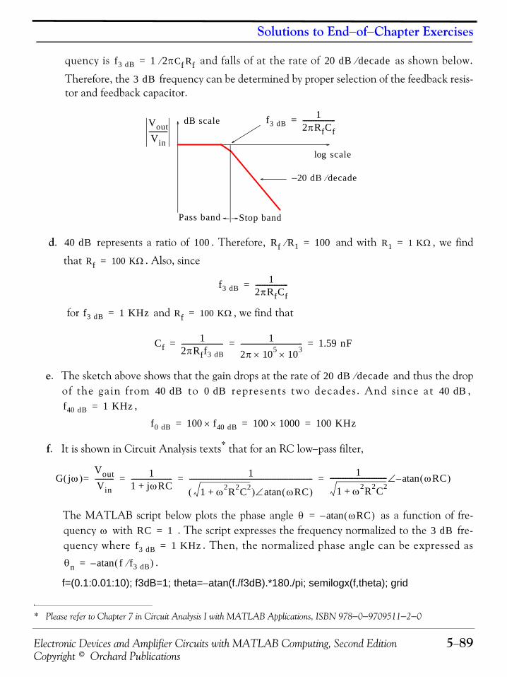
Electronic Devices and Amplifier Circuits with MATLAB Computing, Second Edition 5−89Copyright © Orchard Publications
Solutions to End−of−Chapter Exercises
quency is and falls of at the rate of as shown below.
Therefore, the frequency can be determined by proper selection of the feedback resis-tor and feedback capacitor.
d. represents a ratio of . Therefore, and with , we find
that . Also, since
for and , we find that
e. The sketch above shows that the gain drops at the rate of and thus the dropof the gain from to represents two decades. And since at ,
,
f. It is shown in Circuit Analysis texts* that for an RC low−pass filter,
The MATLAB script below plots the phase angle as a function of fre-quency with . The script expresses the frequency normalized to the fre-quency where . Then, the normalized phase angle can be expressed as
.
f=(0.1:0.01:10); f3dB=1; theta=−atan(f./f3dB).*180./pi; semilogx(f,theta); grid
* Please refer to Chapter 7 in Circuit Analysis I with MATLAB Applications, ISBN 978−0−9709511−2−0
f3 dB 1 2πCf Rf⁄= 20 dB decade⁄
3 dB
dB scale
log scale
VoutVin-----------
Pass band Stop band
f3 dB1
2πRfCf-------------------=
20 dB decade⁄–
40 dB 100 Rf R1⁄ 100= R1 1 KΩ=
Rf 100 KΩ=
f3 dB1
2πRfCf-------------------=
f3 dB 1 KHz= Rf 100 KΩ=
Cf1
2πRff3 dB------------------------ 1
2π 105× 103×------------------------------------ 1.59 nF= = =
20 dB decade⁄40 dB 0 dB 40 dB
f40 dB 1 KHz=
f0 dB 100 f40 dB× 100 1000× 100 KHz= = =
G jω( )VoutVin-----------= 1
1 jωRC+------------------------ 1
1 ω2R2C2+( ) ωRC( )atan∠------------------------------------------------------------------------ 1
1 ω2R2C2+--------------------------------- ωRC( )atan–∠= = =
θ ωRC( )atan–=
ω RC 1 = 3 dBf3 dB 1 KHz=
θn f f3 dB⁄( )atan–=
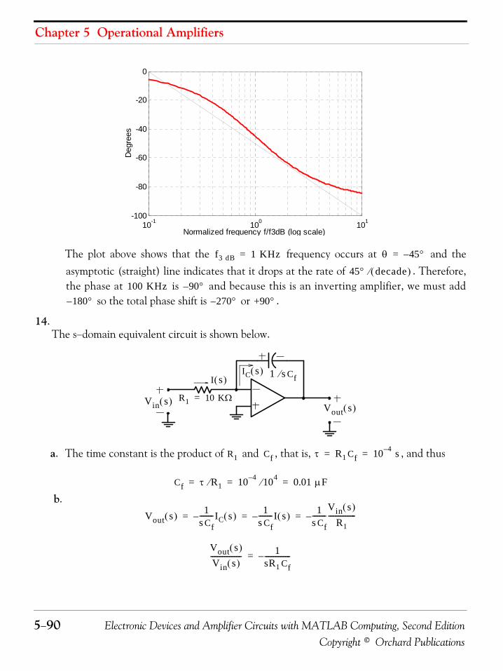
Chapter 5 Operational Amplifiers
5−90 Electronic Devices and Amplifier Circuits with MATLAB Computing, Second EditionCopyright © Orchard Publications
The plot above shows that the frequency occurs at and theasymptotic (straight) line indicates that it drops at the rate of . Therefore,the phase at is and because this is an inverting amplifier, we must add
so the total phase shift is or .
14. The s−domain equivalent circuit is shown below.
a. The time constant is the product of and , that is, , and thus
b.
10-1
100
101
-100
-80
-60
-40
-20
0
Normalized frequency f/f3dB (log scale)
Deg
rees
f3 dB 1 KHz= θ 45°–=
45° decade( )⁄100 KHz 90°–
180°– 270°– +90°
1 s Cf⁄
R1 10 KΩ=
I s( )IC s( )
Vin s( ) Vout s( )
R1 Cf τ R1 Cf 10 4– s= =
Cf τ R1⁄ 10 4– 104⁄ 0.01 μF= = =
Vout s( ) 1s Cf--------IC s( )–
1s Cf--------I s( )–
1s Cf--------
Vin s( )
R1----------------–= = =
Vout s( )Vin s( )------------------ 1
sR1 Cf---------------–=
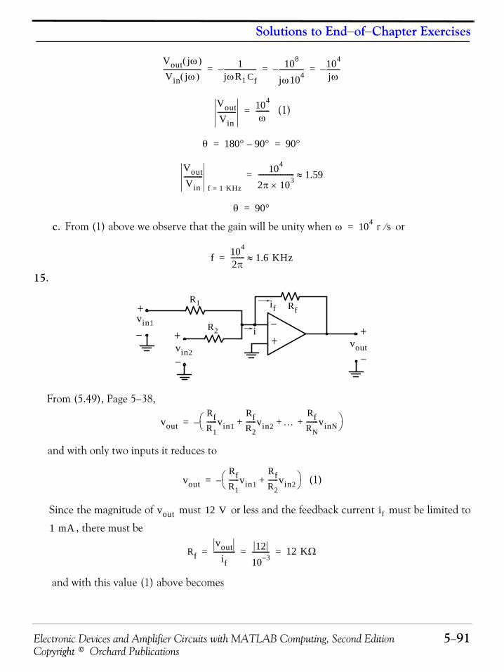
Electronic Devices and Amplifier Circuits with MATLAB Computing, Second Edition 5−91Copyright © Orchard Publications
Solutions to End−of−Chapter Exercises
(1)
c. From (1) above we observe that the gain will be unity when or
15.
From (5.49), Page 5−38,
and with only two inputs it reduces to
(1)
Since the magnitude of must or less and the feedback current must be limited to
, there must be
and with this value (1) above becomes
Vout jω( )Vin jω( )---------------------- 1
jωR1 Cf-------------------– 108
jω104--------------– 104
jω--------–= = =
VoutVin----------- 104
ω--------=
θ 180° 90°– 90°= =
VoutVin-----------
f 1 KHz=
104
2π 103×--------------------- 1.59≈=
θ 90°=
ω 104 r s⁄=
f 104
2π-------- 1.6 KHz≈=
Rfvin1
+
−
−
+vout
R1
R2+
−vin2
if
+−
i
voutRfR1------vin1
RfR2------vin2 …
RfRN-------vinN+ + +⎝ ⎠
⎛ ⎞–=
voutRfR1------vin1
RfR2------vin2+⎝ ⎠
⎛ ⎞–=
vout 12 V if
1 mA
Rfvout
if------------- 12
10 3–---------- 12 KΩ= = =
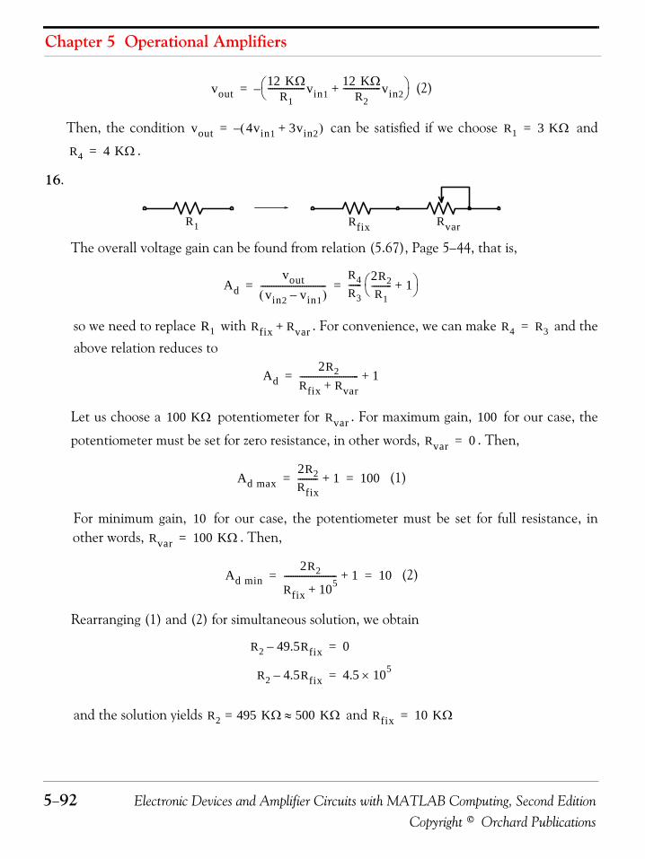
Chapter 5 Operational Amplifiers
5−92 Electronic Devices and Amplifier Circuits with MATLAB Computing, Second EditionCopyright © Orchard Publications
(2)
Then, the condition can be satisfied if we choose and
.
16.
The overall voltage gain can be found from relation (5.67), Page 5−44, that is,
so we need to replace with . For convenience, we can make and theabove relation reduces to
Let us choose a potentiometer for . For maximum gain, for our case, the
potentiometer must be set for zero resistance, in other words, . Then,
(1)
For minimum gain, for our case, the potentiometer must be set for full resistance, inother words, . Then,
(2)
Rearranging (1) and (2) for simultaneous solution, we obtain
and the solution yields and
vout12 KΩ
R1-----------------vin1
12 KΩR2
-----------------vin2+⎝ ⎠⎛ ⎞–=
vout 4vin1 3vin2+( )–= R1 3 KΩ=
R4 4 KΩ=
RfixR1 Rvar
Advout
vin2 vin1–( )------------------------------
R4R3------ 2R2
R1--------- 1+⎝ ⎠
⎛ ⎞= =
R1 Rfix Rvar+ R4 R3=
Ad2R2
Rfix Rvar+--------------------------- 1+=
100 KΩ Rvar 100
Rvar 0=
Ad max2R2Rfix--------- 1+ 100= =
10Rvar 100 KΩ=
Ad min2R2
Rfix 105+------------------------ 1+ 10= =
R2 49.5Rfix– 0=
R2 4.5Rfix– 4.5 105×=
R2 495 KΩ= 500 KΩ≈ Rfix 10 KΩ=
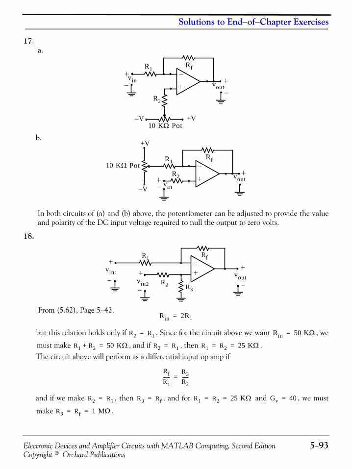
Electronic Devices and Amplifier Circuits with MATLAB Computing, Second Edition 5−93Copyright © Orchard Publications
Solutions to End−of−Chapter Exercises
17.a.
b.
In both circuits of (a) and (b) above, the potentiometer can be adjusted to provide the valueand polarity of the DC input voltage required to null the output to zero volts.
18.
From (5.62), Page 5−42,
but this relation holds only if . Since for the circuit above we want , we
must make , and if , then .The circuit above will perform as a differential input op amp if
and if we make , then , and for and , we must
make .
10 KΩ Pot+VV–
R2
vin vout
R1Rf
RfR1
R2
+V
V–
10 KΩ Pot
vin
vout
Rf
vin1 vout
R1
R2
+
−vin2 R3
+++
−
−
−
Rin 2R1=
R2 R1= Rin 50 KΩ=
R1 R2+ 50 KΩ= R2 R1= R1 R2 25 KΩ= =
RfR1------
R3R2------=
R2 R1= R3 Rf= R1 R2 25 KΩ= = Gv 40=
R3 Rf 1 MΩ= =

Chapter 5 Operational Amplifiers
5−94 Electronic Devices and Amplifier Circuits with MATLAB Computing, Second EditionCopyright © Orchard Publications
19. The circuit is shown below.
By the voltage division expression
and since
it follows that
This is a differential input amplifier and the current is
Next,
s domain–
RfR1
R2−
++
+ −
−Vin s( )
1 sC⁄
I s( )
V1
V2
I s( )
Vout s( )
V2R2
1 sC⁄ R2+--------------------------Vin s( )=
V1 V2=
V1R2
1 sC⁄ R2+--------------------------Vin s( )=
I s( )
I s( )Vin s( ) V1–
R1----------------------------=
I s( ) 1R1------ Vin s( )
R21 sC⁄ R2+--------------------------Vin s( )–⎝ ⎠
⎛ ⎞ Vin s( )R1
--------------- 1R2
1 sC⁄ R2+--------------------------–⎝ ⎠
⎛ ⎞= =
I s( )Vin s( )
R1---------------
1 sC⁄ R2+
1 sC⁄ R2+--------------------------
R21 sC⁄ R2+--------------------------–⎝ ⎠
⎛ ⎞ Vin s( )R1
--------------- 1 sC⁄1 sC⁄ R2+--------------------------⎝ ⎠
⎛ ⎞= =
Vout s( ) V1 RfI s( )–=
Vout s( )R2
1 sC⁄ R2+--------------------------Vin s( ) Rf
Vin s( )R1
--------------- 1 sC⁄1 sC⁄ R2+--------------------------⎝ ⎠
⎛ ⎞–=
Gv s( )Vout s( )Vin s( )
------------------R2
1 sC⁄ R2+--------------------------
RfR1------ 1 sC⁄
1 sC⁄ R2+--------------------------⎝ ⎠
⎛ ⎞–R1R2 Rf sC⁄–
R1 1 sC⁄ R2+( )-------------------------------------= = =
Gv s( )Vout s( )
Vin s( )------------------
R2 Rf sCR1⁄–
R2 1 sC⁄+----------------------------------
sCR2 Rf R1⁄–
sCR2 1+----------------------------------
s Rf CR1R2⁄–
s 1 CR2⁄+-----------------------------------= = = =
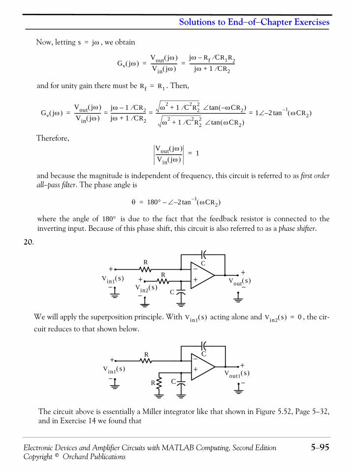
Electronic Devices and Amplifier Circuits with MATLAB Computing, Second Edition 5−95Copyright © Orchard Publications
Solutions to End−of−Chapter Exercises
Now, letting , we obtain
and for unity gain there must be . Then,
Therefore,
and because the magnitude is independent of frequency, this circuit is referred to as first orderall−pass filter. The phase angle is
where the angle of is due to the fact that the feedback resistor is connected to theinverting input. Because of this phase shift, this circuit is also referred to as a phase shifter.
20.
We will apply the superposition principle. With acting alone and , the cir-cuit reduces to that shown below.
The circuit above is essentially a Miller integrator like that shown in Figure 5.52, Page 5−32,and in Exercise 14 we found that
s jω=
Gv jω( )Vout jω( )
Vin jω( )----------------------
jω Rf CR1R2⁄–
jω 1 CR2⁄+--------------------------------------= =
Rf R1=
Gv jω( )Vout jω( )Vin jω( )----------------------
jω 1 CR2⁄–
jω 1 CR2⁄+-----------------------------
ω2 1 C2R22⁄+ ωCR2–( )tan∠
ω2 1 C2R22⁄+ ωCR2( )tan∠
--------------------------------------------------------------------------- 1 2 ωCR2( )1–tan–∠= = ==
Vout jω( )
Vin jω( )---------------------- 1=
θ 180° 2 ωCR2( )1–tan–∠–=
180°
Vin1 s( ) +
−−
+Vout s( )
R
R+
− Vin2 s( )
C
C
+−
Vin1 s( ) Vin2 s( ) 0=
+−
Vin1 s( )
−
+Vout1 s( )
R
R
+
− C
C
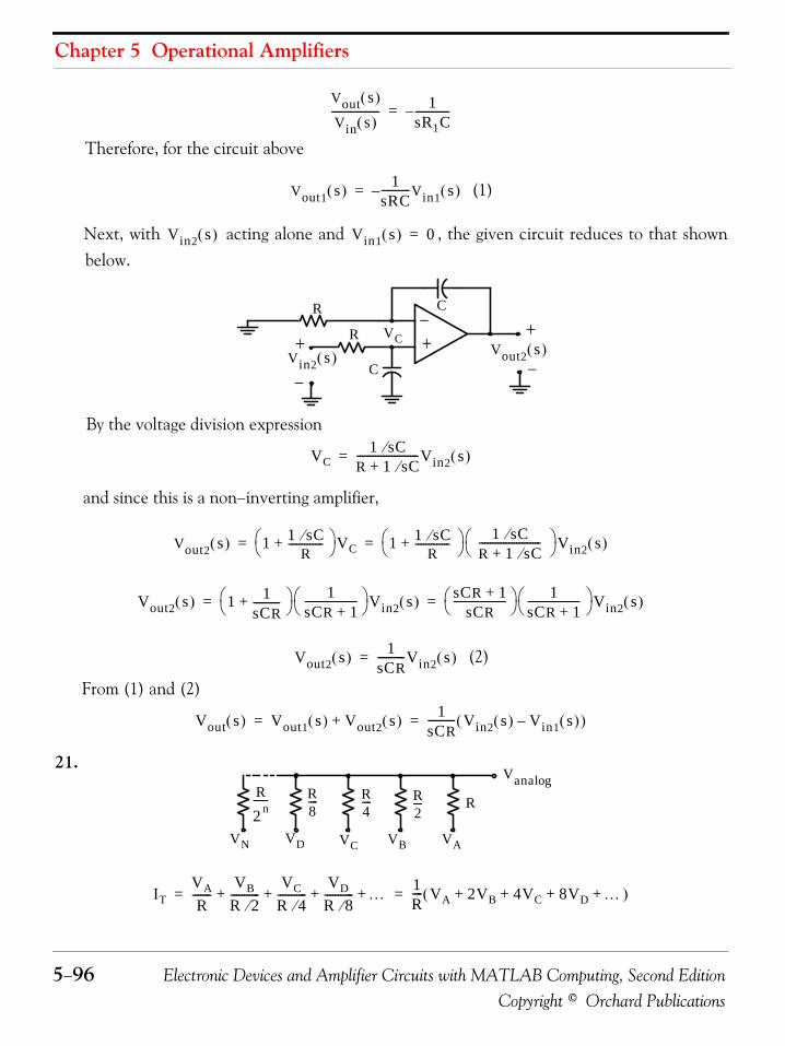
Chapter 5 Operational Amplifiers
5−96 Electronic Devices and Amplifier Circuits with MATLAB Computing, Second EditionCopyright © Orchard Publications
Therefore, for the circuit above
(1)
Next, with acting alone and , the given circuit reduces to that shownbelow.
By the voltage division expression
and since this is a non−inverting amplifier,
(2)
From (1) and (2)
21.
Vout s( )
Vin s( )------------------ 1
sR1C-------------–=
Vout1 s( ) 1sRC-----------Vin1 s( )–=
Vin2 s( ) Vin1 s( ) 0=
+−
+
−−
+Vout2 s( )
R
RVin2 s( )
C
VC
C
VC1 sC⁄
R 1 sC⁄+-----------------------Vin2 s( )=
Vout2 s( ) 1 1 sC⁄R
-------------+⎝ ⎠⎛ ⎞ VC 1 1 sC⁄
R-------------+⎝ ⎠
⎛ ⎞ 1 sC⁄R 1 sC⁄+-----------------------⎝ ⎠
⎛ ⎞ Vin2 s( )= =
Vout2 s( ) 1 1sCR----------+⎝ ⎠
⎛ ⎞ 1sCR 1+--------------------⎝ ⎠
⎛ ⎞ Vin2 s( ) sCR 1+sCR
--------------------⎝ ⎠⎛ ⎞ 1
sCR 1+--------------------⎝ ⎠
⎛ ⎞ Vin2 s( )= =
Vout2 s( ) 1sCR----------Vin2 s( )=
Vout s( ) Vout1 s( ) Vout2 s( )+1
sCR---------- Vin2 s( ) Vin1 s( )–( )= =
Vanalog
VBVCVD VAVN
RR2----R
4----R
8----R
2 n------
ITVAR
-------VB
R 2⁄-----------
VCR 4⁄-----------
VDR 8⁄----------- …+ + + +
1R---- VA 2VB 4VC 8VD …+ + + +( )= =

Electronic Devices and Amplifier Circuits with MATLAB Computing, Second Edition 5−97Copyright © Orchard Publications
Solutions to End−of−Chapter Exercises
or
22.
We write nodal equations at Nodes 1, 2, and 3.
Simplifying and collecting like terms we obtain
By Cramer’s rule*
* For a review of matrices and determinants please refer to Numerical Analysis Using MATLAB and Excel, ISBN 978−1−934404−03−4.
1Req--------- 1
R---- 1
R 2⁄----------- 1
R 4⁄----------- 1
R 8⁄----------- …+ + + +=
ReqR
1 2 4 8 …+ + + +-------------------------------------------=
Vanalog ReqITR
1 2 4 8 …+ + + +------------------------------------------- 1
R---- VA 2VB 4VC 8VD …+ + + +( )⋅= =
VanalogVA 2VB 4VC 8VD …+ + + +
1 2 4 8 …+ + + +------------------------------------------------------------------------------=
VA VB VC VD
R R R2R2R 2R 2R 2R
Vanalog1 2 3
V1 V2 V3
V12R-------
V1 VA–
2R--------------------
V1 V2–
R-------------------+ + 0=
V2 V1–
R-------------------
V2 VB–
2R--------------------
V2 V3–
R-------------------+ + 0=
V3 V2–
R-------------------
V3 VC–
2R--------------------
V3 VD–
R 2R+--------------------+ + 0=
4V1 2V2– VA=
2– V1 5V2 2V3–+ VB=
6– V2 11V3+ 3VC 2VD+=
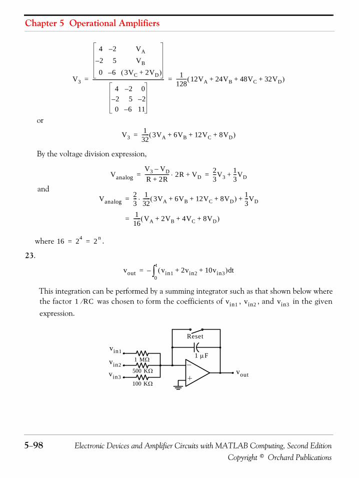
Chapter 5 Operational Amplifiers
5−98 Electronic Devices and Amplifier Circuits with MATLAB Computing, Second EditionCopyright © Orchard Publications
or
By the voltage division expression,
and
where .
23.
This integration can be performed by a summing integrator such as that shown below wherethe factor was chosen to form the coefficients of , , and in the givenexpression.
V3
4 2– VA
2– 5 VB
0 6– 3VC 2VD+( )
4 2– 02– 5 2–
0 6– 11
----------------------------------------------------------- 1128--------- 12VA 24VB 48VC 32VD+ + +( )= =
V31
32------ 3VA 6VB 12VC 8VD+ + +( )=
VanalogV3 VD–
R 2R+-------------------- 2R⋅ VD+
23---V3
13---VD+= =
Vanalog23--- 1
32------ 3VA 6VB 12VC 8VD+ + +( )⋅ 1
3---VD+=
116------ VA 2VB 4VC 8VD+ + +( )=
16 24 2 n= =
vout vin1 2vin2 10vin3+ +( ) td0
t
∫–=
1 RC⁄ vin1 vin2 vin3
1 μF1 MΩ
Reset
vin1
500 KΩ
100 KΩ
vin3
vin2vout

Electronic Devices and Amplifier Circuits with MATLAB Computing, Second Edition 5−99Copyright © Orchard Publications
Solutions to End−of−Chapter Exercises
24.
(1)
(2)
Substitution of (1) into (2) yields
Since we want , we choose and
25.
(1)
(2)
Differentiating (1) with respect to we obtain
(3)
and from (1), (2), and (3)
R1
CRf
voutvin
ii
ivinR1------- C
dvindt
----------+=
vout Rf i–=
voutRfR1------– vin Rf C
dvindt
----------–=
vout 5vin– 3dvin dt⁄–= Rf 5R1= Rf C 3=
vin
C
R1
R2 L
vout
i i
ivinR1------- C
dvindt
----------+=
vout R2i– Ldidt-----–=
t
didt----- 1
R1------
dvindt
---------- Cd2vin
dt2-------------+=
voutR2R1------vin R2C
dvindt
---------- LR1------
dvindt
---------- LCd2vin
dt2-------------+ + +
⎝ ⎠⎜ ⎟⎛ ⎞
–=
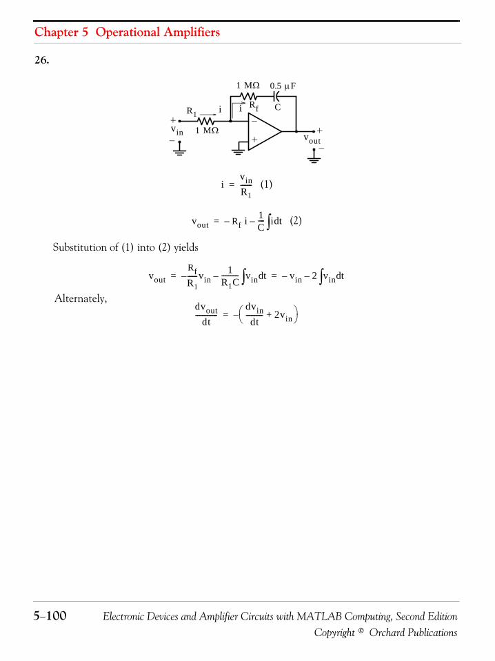
Chapter 5 Operational Amplifiers
5−100 Electronic Devices and Amplifier Circuits with MATLAB Computing, Second EditionCopyright © Orchard Publications
26.
(1)
(2)
Substitution of (1) into (2) yields
Alternately,
vin vout1 MΩ
1 MΩ 0.5 μF
R1 i Rfi C
ivinR1-------=
vout Rf i–1C---- i td∫–=
voutRfR1------– vin
1R1C---------- vin td∫– vin– 2 vin td∫–= =
dvoutdt
-------------dvindt
---------- 2vin+⎝ ⎠⎛ ⎞–=
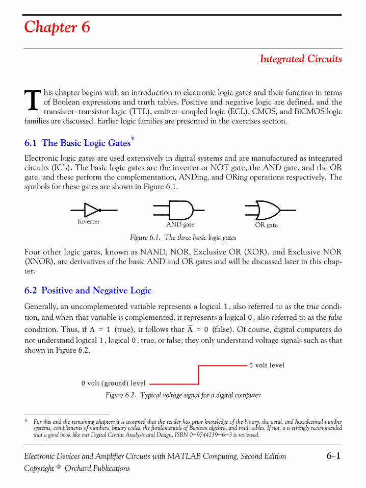
Electronic Devices and Amplifier Circuits with MATLAB Computing, Second Edition 6−1Copyright © Orchard Publications
Chapter 6
Integrated Circuits
his chapter begins with an introduction to electronic logic gates and their function in termsof Boolean expressions and truth tables. Positive and negative logic are defined, and thetransistor−transistor logic (TTL), emitter−coupled logic (ECL), CMOS, and BiCMOS logic
families are discussed. Earlier logic families are presented in the exercises section.
6.1 The Basic Logic Gates*
Electronic logic gates are used extensively in digital systems and are manufactured as integratedcircuits (IC’s). The basic logic gates are the inverter or NOT gate, the AND gate, and the ORgate, and these perform the complementation, ANDing, and ORing operations respectively. Thesymbols for these gates are shown in Figure 6.1.
Figure 6.1. The three basic logic gates
Four other logic gates, known as NAND, NOR, Exclusive OR (XOR), and Exclusive NOR(XNOR), are derivatives of the basic AND and OR gates and will be discussed later in this chap-ter.
6.2 Positive and Negative Logic
Generally, an uncomplemented variable represents a logical , also referred to as the true condi-tion, and when that variable is complemented, it represents a logical , also referred to as the falsecondition. Thus, if (true), it follows that (false). Of course, digital computers donot understand logical , logical , true, or false; they only understand voltage signals such as thatshown in Figure 6.2.
Figure 6.2. Typical voltage signal for a digital computer
* For this and the remaining chapters it is assumed that the reader has prior knowledge of the binary, the octal, and hexadecimal numbersystems, complements of numbers, binary codes, the fundamentals of Boolean algebra, and truth tables. If not, it is strongly recommendedthat a good book like our Digital Circuit Analysis and Design, ISBN 0−9744239−6−3 is reviewed.
T
Inverter AND gate OR gate
10
A 1= A 0=
1 0
0 volt ground( ) level
5 volt level
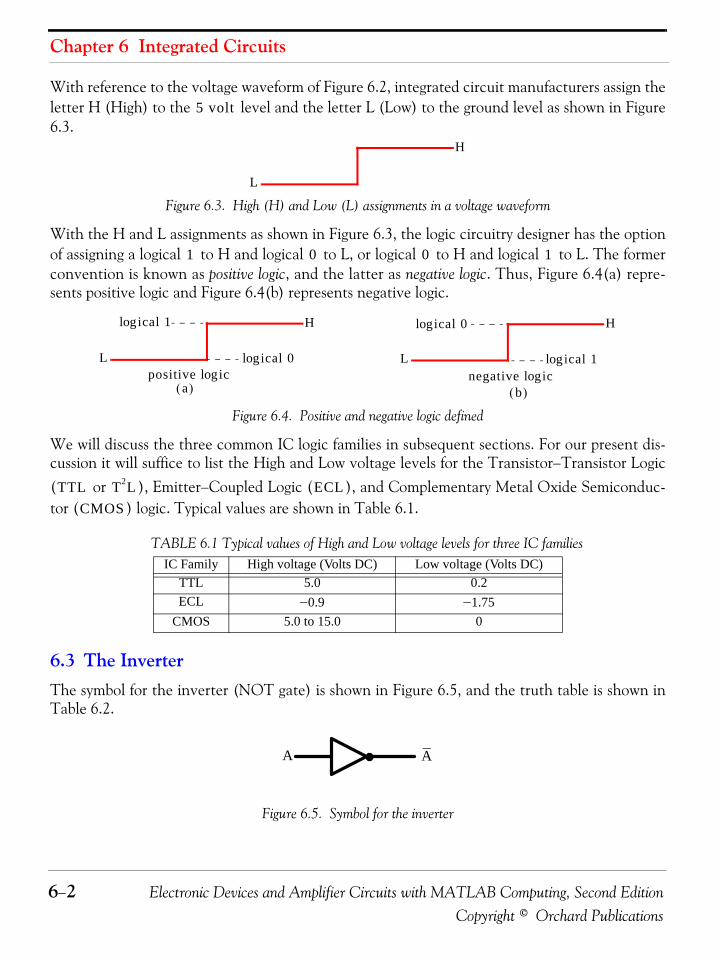
Chapter 6 Integrated Circuits
6−2 Electronic Devices and Amplifier Circuits with MATLAB Computing, Second EditionCopyright © Orchard Publications
With reference to the voltage waveform of Figure 6.2, integrated circuit manufacturers assign theletter H (High) to the level and the letter L (Low) to the ground level as shown in Figure6.3.
Figure 6.3. High (H) and Low (L) assignments in a voltage waveform
With the H and L assignments as shown in Figure 6.3, the logic circuitry designer has the optionof assigning a logical to H and logical to L, or logical to H and logical to L. The formerconvention is known as positive logic, and the latter as negative logic. Thus, Figure 6.4(a) repre-sents positive logic and Figure 6.4(b) represents negative logic.
Figure 6.4. Positive and negative logic defined
We will discuss the three common IC logic families in subsequent sections. For our present dis-cussion it will suffice to list the High and Low voltage levels for the Transistor−Transistor Logic( or ), Emitter−Coupled Logic ( ), and Complementary Metal Oxide Semiconduc-tor ( ) logic. Typical values are shown in Table 6.1.
6.3 The InverterThe symbol for the inverter (NOT gate) is shown in Figure 6.5, and the truth table is shown inTable 6.2.
Figure 6.5. Symbol for the inverter
TABLE 6.1 Typical values of High and Low voltage levels for three IC familiesIC Family High voltage (Volts DC) Low voltage (Volts DC)
TTL 5.0 0.2ECL −0.9 −1.75
CMOS 5.0 to 15.0 0
5 volt
L
H
1 0 0 1
L
H
L
H
ical 0log
ical 0log
positive iclogical 1log
ical 1log
negative iclogb( )a( )
TTL T2L ECLCMOS
AA

Electronic Devices and Amplifier Circuits with MATLAB Computing, Second Edition 6−3Copyright © Orchard Publications
The Inverter
With positive logic, the truth table for the inverter is written as shown in Table 6.3.
With negative logic, the truth table for the inverter is written as shown in Table 6.4.
Figure 6.6 shows the TTL SN7404 Hex Inverter IC where SN identifies the packaging and Heximplies that there are 6 inverters within the IC.
Figure 6.6. The SN7404 Hex Inverter IC
One important parameter is the input clamp voltage denoted as and this refers to the maximumnegative voltage that may be applied at the input terminals without damaging the IC. A typicalvalue for this parameter is . To insure that this value is not exceeded, diode is includedto clamp the input voltage to less than with respect to the ground. We recall from Chapter2 that a practical diode, when forward−biased, may be represented as an ideal diode in series witha source and a small resistance as shown in Figure 6.7.
TABLE 6.2 The truth table for the inverterInput Output
L HH L
TABLE 6.3 The truth table for the inverter when positive logic is assumedInput Output
0 11 0
TABLE 6.4 The truth table for the inverter when negative logic is assumedInput Output
1 00 1
1
2
3
6A
Vcc
7
6
4
6Y
5A
4A
4Y
5 5Y
1A
2Y
2A
1Y
3Y
3A
GND
14
8
9
10
11
12
13
1 2 43 5 6
8
7
91011121314
GND
Vcc
A2A1 A3
A4A5A6
Y1 Y2 Y3
Y4Y5Y6
VIK
1.2 V– D1
1.2 V–
0.7 V

Chapter 6 Integrated Circuits
6−4 Electronic Devices and Amplifier Circuits with MATLAB Computing, Second EditionCopyright © Orchard Publications
Figure 6.7. Practical and ideal diode representation
The data sheets provided by the manufacturer list several parameters and we will discuss themost important later in this chapter.
Figure 6.8 shows the internal details of the TTL IC 7404 inverter.
Figure 6.8. Circuit of the SN7404 Inverter
Note: Unless otherwise noted, henceforth Low will mean a nominal input or output signaland High will mean a nominal input or output signal.
The inverter circuit of Figure 6.8 functions as follows:
We assume that the input voltage is the output of a previous stage and it is Low at
with respect to the ground as shown in Figure 6.9. With this input, transistor is ON and thevoltage at the collector of transistor is and under
this condition, transistors and are both OFF. This is because if transistors and were
vD V( )
iD mA( )vD
slope R=
0.7
Practical
0.7 V
RIdeal
diode diode
+Vcc
+
-
4 Κ Ω
1 Κ Ω
1 .6 Κ Ω 1 3 0 Ω
Input A
Output Y
T1
T3
T2
T4
D1
D2
0 V5 V
Vin 0.2 V=
T1
V1 T1 V1 VCE sat Vin+ 0.2 0.2+ 0.4 V= = =
T2 T3 T2 T3

Electronic Devices and Amplifier Circuits with MATLAB Computing, Second Edition 6−5Copyright © Orchard Publications
The Inverter
both ON, the voltage would have to be . Accord-ingly, we accept the fact that with the input Low, transistors and are both OFF. However,the current that flows through the resistor and then into the base of transistor , is suf-ficient to turn it ON. Then, and thus the out-put is High and the inversion operation has been performed.
Figure 6.9. Circuit of the SN7404 Inverter for Low−to−High inversion
Next, with the input High the circuit is as shown in Figure 6.10 and the circuit functions as fol-lows:
We assume that the input voltage is the output of a previous stage and it is High at with respect to the ground. With this input, the base−emitter junction of transistor is reverse−
biased, current flows from through the resistor and thus the base−collector junction isforward−biased. Under these conditions, transistor is said to be operating at the inverse activemode. The current that flows through the base collector junction of transistor is sufficient toturn transistor ON and this causes transistor to turn ON also. The voltage at the collec-tor of transistor is . However, this voltage is not suffi-cient to turn transistor ON because for transistor to be ON there should be
. Therefore, we conclude that transistor is
OFF, , and thus the output is Low and the inversion operation has been performed.
V1 V1 VBE T2 VBE T3+ 0.7 0.7+ 1.4 V= = =
T2 T3
I 1.6 KΩ T4
Vout VCC VCE T4– VD2– 5.0 0.2– 0.7– 4.1 V= = =
+Vcc
+
-
4 Κ Ω
1 Κ Ω
1 .6 Κ Ω 1 3 0 Ω
Input A
Output Y
T1
T3
T2
T4
D1
D2
Vin 0.2 V=
ON
V1
OFF
ONI
VCE sat0.2 V
Vout 4.1 V=
OFF
Vin 5.0 V=
T1
VCC 4 KΩ
T1
T1
T2 T3 V2
T2 V2 VCE T2 VBE T3+ 0.2 0.7+ 0.9 V= = =
T4 T4
V2 VBE T4 VD2 Vout+ + 0.7 0.7 0.2+ + 1.6 V= = = T4
Vout 0.2 V=

Chapter 6 Integrated Circuits
6−6 Electronic Devices and Amplifier Circuits with MATLAB Computing, Second EditionCopyright © Orchard Publications
Figure 6.10. Circuit of the SN7404 Inverter for High−to−Low inversion
It should be noted that it is the diode that prevents transistor from being ON; if werenot being there, would be also ON since there would be which isjust sufficient to turn ON.
6.4 The AND GateThe symbol for a 3−input AND gate is shown in Figure 6.11, and the truth table is shown inTable 6.5.
Figure 6.11. 3−input AND gate symbol
With positive logic, the truth table for a 3−input AND gate is written as shown in Table 6.6.
Table 6.6 shows that the output of an AND gate is logical (true) only when all inputs are logi-cal .
Figure 6.12 shows the TTL SN7408 Quad 2−input AND gate where Quad implies that there are4 AND gates within the IC.
+Vcc
+
-
4 Κ Ω
1 Κ Ω
1 .6 Κ Ω 1 3 0 Ω
Input A
Output Y
T1
T3
T2
T4
D1
D2
OFFV2
0.2 V
ONVin 5.0 V=
Acts as diode
Vout 0.2 V=
ON
0.7 V
D2 T4 D2
T4 VBE T4 0.9 0.2– 0.7 V= =
T4
A
CB D
11

Electronic Devices and Amplifier Circuits with MATLAB Computing, Second Edition 6−7Copyright © Orchard Publications
The AND Gate
Figure 6.12. The SN7408 Quad 2−input AND gate
Figure 6.13 shows the internal details of a two−input TTL AND gate. We will defer the analysis ofthis circuit and the reason for deferring the discussion after we introduce the NAND gate.
TABLE 6.5 Truth table for 3−input AND gateInputs Output
A B C DL L L LL L H LL H L LL H H LH L L LH L H LH H L LH H H H
TABLE 6.6 Truth table of 3−input AND gate when positive logic is usedInputs Output
A B C D0 0 0 00 0 1 00 1 0 00 1 1 01 0 0 01 0 1 01 1 0 01 1 1 1
1
2
3
4B
Vcc
7
6
4
4A
4Y
3A
3Y
5 3B
1A
2A
1Y
1B
2Y
2B
GND
14
8
9
10
11
12
13
1A
1B1Y
2A
3A
2Y2B
3B3Y
4A
4B4Y
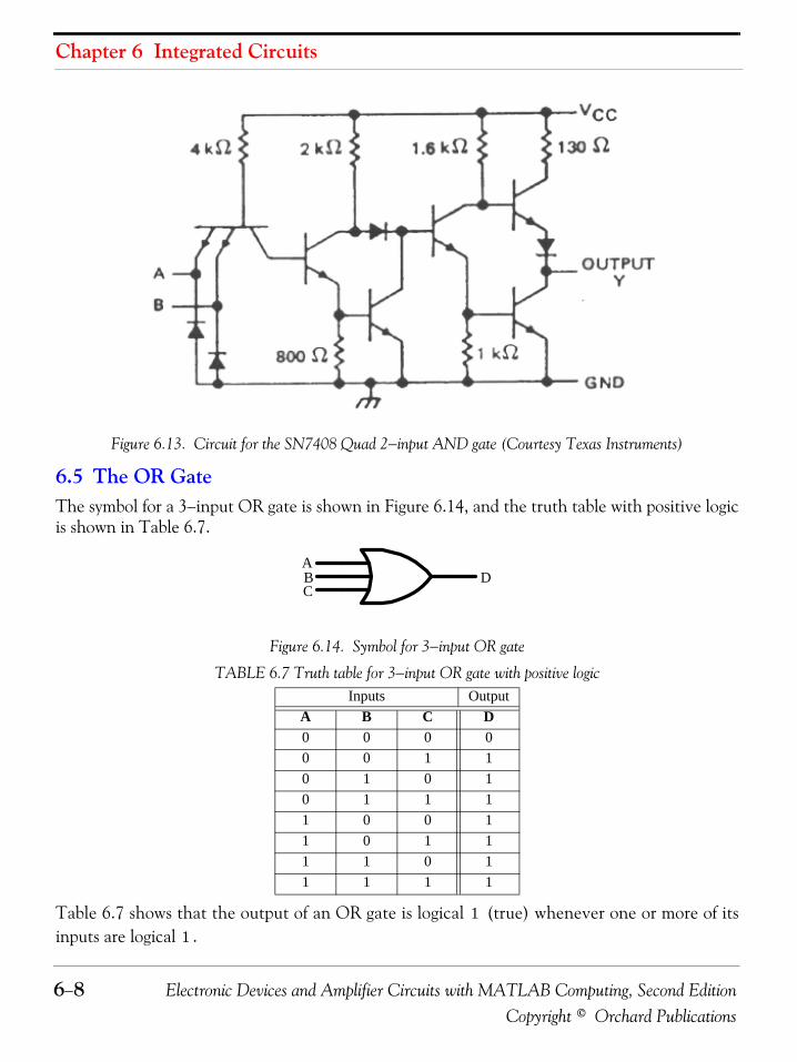
Chapter 6 Integrated Circuits
6−8 Electronic Devices and Amplifier Circuits with MATLAB Computing, Second EditionCopyright © Orchard Publications
Figure 6.13. Circuit for the SN7408 Quad 2−input AND gate (Courtesy Texas Instruments)
6.5 The OR GateThe symbol for a 3−input OR gate is shown in Figure 6.14, and the truth table with positive logicis shown in Table 6.7.
Figure 6.14. Symbol for 3−input OR gate
Table 6.7 shows that the output of an OR gate is logical (true) whenever one or more of itsinputs are logical .
TABLE 6.7 Truth table for 3−input OR gate with positive logicInputs Output
A B C D0 0 0 00 0 1 10 1 0 10 1 1 11 0 0 11 0 1 11 1 0 11 1 1 1
A
CB D
11
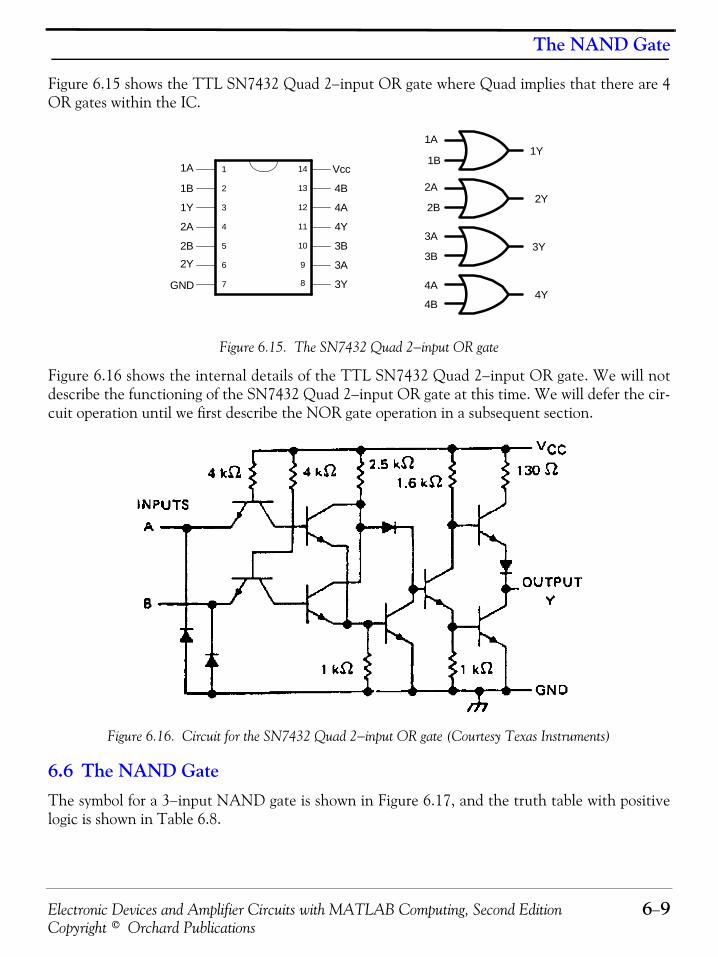
Electronic Devices and Amplifier Circuits with MATLAB Computing, Second Edition 6−9Copyright © Orchard Publications
The NAND Gate
Figure 6.15 shows the TTL SN7432 Quad 2−input OR gate where Quad implies that there are 4OR gates within the IC.
Figure 6.15. The SN7432 Quad 2−input OR gate
Figure 6.16 shows the internal details of the TTL SN7432 Quad 2−input OR gate. We will notdescribe the functioning of the SN7432 Quad 2−input OR gate at this time. We will defer the cir-cuit operation until we first describe the NOR gate operation in a subsequent section.
Figure 6.16. Circuit for the SN7432 Quad 2−input OR gate (Courtesy Texas Instruments)
6.6 The NAND GateThe symbol for a 3−input NAND gate is shown in Figure 6.17, and the truth table with positivelogic is shown in Table 6.8.
1
2
3
4B
Vcc
7
6
4
4A
4Y
3A
3Y
5 3B
1A
2A
1Y
1B
2Y
2B
GND
14
8
9
10
11
12
13
1A
1B1Y
2A
2B2Y
3Y3A
3B
4A4Y
4B

Chapter 6 Integrated Circuits
6−10 Electronic Devices and Amplifier Circuits with MATLAB Computing, Second EditionCopyright © Orchard Publications
Figure 6.17. Symbol for 3−input NAND gate
Table 6.8 shows that the output of an NAND gate is logical (false) only when all inputs arelogical .
Figure 6.18 shows the TTL SN7400 Quad 2−input NAND gate where Quad implies that thereare 4 NAND gates within the IC.
Figure 6.18. The SN7400 Quad 2−input NAND gate
Figure 6.19 shows the internal details of the IC SN7400 NAND gate where transistor isequivalent to two identical NPN transistors with their bases and collectors tied together; there-fore, they are fabricated as a single device with 2 emitters but only one collector and one base asshown in Figure 6.19.
TABLE 6.8 Truth table for 3−input NAND gate with positive logicInputs Output
A B C D0 0 0 10 0 1 10 1 0 10 1 1 11 0 0 11 0 1 11 1 0 11 1 1 0
DBC
A
01
1Y
3A
1A
1B
2B
2A2Y
3B3Y
4A
4B4Y
1
2
3
4B
Vcc
7
6
4
4A
4Y
3A
3Y
5 3B
1A
2A
1Y
1B
2Y
2B
GND
14
8
9
10
11
12
13
T1

Electronic Devices and Amplifier Circuits with MATLAB Computing, Second Edition 6−11Copyright © Orchard Publications
The NAND Gate
Figure 6.19. Circuit for the TTL SN7400 Quad 2−input NAND gate
We observe that, with the exception of two inputs for the 2−input NAND gate, this circuit ispractically the same as that of the inverter circuit of Figure 6.8 where transistor is stacked ontop of transistor and the operation is complementary, that is, when transistor is ON transis-tor is OFF and vice versa. This arrangement is referred to as totem−pole configuration. The 2−input TTL NAND gate circuit of Figure 6.19 functions as follows:
Let us assume that either Input A or B or both are Low at with respect to the ground
as shown in Figure 6.20. Under any of these three conditions, transistor is ON and the voltage at the collector of transistor is and thus transistors
and are both OFF. This is because if transistors and were both ON, the voltage would have to be . Accordingly, we accept the fact thatunder any of these three conditions, transistors and are both OFF. However, The current that flows through the resistor and then into the base of transistor is sufficient to turnit ON. Then, and thus the output is Highand this satisfies the 2−input NAND gate operation.
+Vcc
+
-
4 Κ Ω
1 Κ Ω
1.6 Κ Ω 1 3 0 Ω
Input A
Output Y
T1
T3
T2
T4
D1
Input B
D2
D3
T4
T3 T3
T4
Vin 0.2 V=
T1
V1 T1 V1 VCE sat Vin+ 0.2 0.2+ 0.4 V= = =
T2 T3 T2 T3 V1
V1 VBE T2 VBE T3+ 0.7 0.7+ 1.4 V= = =
T2 T3 I1.6 KΩ T4
Vout VCC VCE T4– VD2– 5.0 0.2– 0.7– 4.1 V= = =

Chapter 6 Integrated Circuits
6−12 Electronic Devices and Amplifier Circuits with MATLAB Computing, Second EditionCopyright © Orchard Publications
Figure 6.20. Circuit of the SN7400 2−input NAND gate when either Input A of B or both are Low
Next, with both inputs High the circuit is as shown in Figure 6.21 and the circuit functions as fol-lows:
With at both inputs, the base−emitter junction of transistor is reverse−biased,current flows from through the resistor and thus the base−collector junction is for-ward−biased. In other words, transistor is operating at the inverse active mode. The currentthat flows through the base collector junction of transistor is sufficient to turn transistor ON and this causes transistor to turn ON also. The voltage at the collector of transistor
is . However, this voltage is not sufficient to turntransistor ON because for transistor to be ON the voltage should have the value
. T h e r e f o r e , t r a n s i s t o r i s O F F ,
, and this satisfies the 2−input NAND gate operation.
It should be noted that it is the diode that prevents transistor from being ON; if werenot being there, would be also ON since there would be which is
+Vcc
+
-
4 Κ Ω
1 Κ Ω
1.6 Κ Ω 1 3 0 Ω
Input A
Output Y
T1
T3
T2
T4
D1
Input B
D2
D3
Vin 0.2 V=
ON
VCE sat0.2 V
V1
OFF
ONI
OFF
Vout 4.1 V=
Vin 5.0 V= T1
VCC 4 KΩ
T1
T1 T2
T3 V2
T2 V2 VCE T2 VBE T3+ 0.2 0.7+ 0.9 V= = =
T4 T4 V2
V2 VBE T4 VD2 Vout+ + 0.7 0.7 0.2+ + 1.6 V= = = T4
VOUT 0.2 V=
D3 T4 D3
T4 VBE T4 0.9 0.2– 0.7 V= =
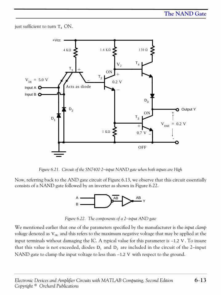
Electronic Devices and Amplifier Circuits with MATLAB Computing, Second Edition 6−13Copyright © Orchard Publications
The NAND Gate
just sufficient to turn ON.
Figure 6.21. Circuit of the SN7400 2−input NAND gate when both inputs are High
Now, referring back to the AND gate circuit of Figure 6.13, we observe that this circuit essentiallyconsists of a NAND gate followed by an inverter as shown in Figure 6.22.
Figure 6.22. The components of a 2−input AND gate
We mentioned earlier that one of the parameters specified by the manufacturer is the input clampvoltage denoted as and this refers to the maximum negative voltage that may be applied at theinput terminals without damaging the IC. A typical value for this parameter is . To insurethat this value is not exceeded, diodes and are included in the circuit of the 2−inputNAND gate to clamp the input voltage to less than with respect to the ground.
T4
+Vcc
+
-
4 Κ Ω
1 Κ Ω
1.6 Κ Ω 1 3 0 Ω
Input A
Output Y
T1
T3
T2
T4
D1
Input B
D2
D3
Vin 5.0 V=
Acts as diode
ON
0.2 V
V2
ON
0.7 V
Vout 0.2 V=
A
BY
ABAB
VIK
1.2 V–
D1 D2
1.2 V–
OFF

Chapter 6 Integrated Circuits
6−14 Electronic Devices and Amplifier Circuits with MATLAB Computing, Second EditionCopyright © Orchard Publications
6.7 The NOR GateThe symbol for a 3−input NOR gate is shown in Figure 6.23, and the truth table with positivelogic is shown in Table 6.9.
Figure 6.23. Symbol for 3−input NOR gate
Table 6.9 shows that the output of an NOR gate is logical (true) only when all inputs are logi-cal (false).
Figure 6.24 shows the TTL SN7402 Quad 2−input NOR gate where Quad implies that there are4 NOR gates within the IC.
Figure 6.24. The TTL SN7402 Quad 2−input NOR gate
Figure 6.25 shows the internal details of the TTL IC SN7402 NOR gate.
TABLE 6.9 Truth table for 3−input NOR gate with positive logicInputs Output
A B C D0 0 0 10 0 1 00 1 0 00 1 1 01 0 0 01 0 1 01 1 0 01 1 1 0
DBC
A
10
1Y
3A
1A
1B
2B
2A2Y
3B3Y
4A
4B4Y
1
2
3
4Y
Vcc
7
6
4
4B
4A
3B
3A
5 3Y
1Y
2Y
1B
1A
2B
2A
GND
14
8
9
10
11
12
13

Electronic Devices and Amplifier Circuits with MATLAB Computing, Second Edition 6−15Copyright © Orchard Publications
The Exclusive OR (XOR) and Exclusive NOR (XNOR) Gates
Figure 6.25. Circuit for the TTL SN7402 Quad 2−input NOR gate
The TTL 2−input NOR gate circuit of Figure 6.25 functions as follows:
When both inputs are Low at with respect to the ground, transistors and are bothON. The voltages at the base of transistors and are the same as the collector voltages oftransistors s and , that is, , and thus transistors and are OFF. However, transis-tor is ON and therefore, .
If Input A is Low and Input B is High, transistor will be ON and transistor will be OFF. Buttransistor will behave as a junction diode turning transistor ON, and a voltage drop acrossthe resistor will be developed and it will be sufficient to turn transistor ON, and thus
. If Input A is High and Input B is Low or both inputs are High, we find that
also.
6.8 The Exclusive OR (XOR) and Exclusive NOR (XNOR) GatesThe exclusive−OR (XOR) logic gate has two inputs and one output. The symbol for the XORgate is shown in Figure 6.26, and the truth table with positive logic is shown in Table 6.10.
We observe that the output of an XOR gate is logical (true) when only one of the inputs, butnot both, is logical .
+Vcc
+
-
4 Κ Ω
1 Κ Ω
1 .6 Κ Ω 1 3 0 Ω
Input A
Output YInput B
D1
D2
T3
T2
T1
D3
4 Κ Ω
T4
T5
T6
0.2 V T1 T2
T3 T4
T1 T2 0.2 V T3 T4
T5 Vout VCC VCE T5– VD5– 5.0 0.2– 0.7– 4.1 V= = =
T1 T3
T2 T4
1 KΩ T6
Vout 0.2 V=
Vout 0.2 V=
11

Chapter 6 Integrated Circuits
6−16 Electronic Devices and Amplifier Circuits with MATLAB Computing, Second EditionCopyright © Orchard Publications
Figure 6.26. Symbol for the XOR gate with positive logic
Figure 6.27 shows the TTL SN7486 Quad XOR gate where Quad implies that there are 4 XORgates within the IC.
Figure 6.27. The TTL SN7486 Quad XOR gate
Figure 6.28 shows the internal details of the TTL IC SN7486 XOR gate.
The exclusive−NOR (XNOR) logic gate has two inputs and one output. The symbol for theXNOR gate is shown in Figure 6.29. and the truth table with positive logic is shown in Table6.11.
Table 6.11 shows that the output of a XNOR gate is logical (true) only when the inputs are thesame, that is, both logical or both logical . For this reason, the XNOR gate is also known asequivalence gate.
There is no IC XNOR gate in the TTL family but one can be formed with an XOR gate(SN7486) followed by an inverter (SN7404). We can also implement the XNOR function usingthe TTL SN7486 IC with negative logic.
TABLE 6.10 Truth table for 2−input XOR gateInputs Output
A B C0 0 00 1 11 0 11 1 0
CBA
1Y
3A
1A
1B
2B
2A2Y
3B3Y
4A
4B4Y
1
2
3
4B
Vcc
7
6
4
4A
4Y
3A
3Y
5 3B
1A
2A
1Y
1B
2Y
2B
GND
14
8
9
10
11
12
13
10 1
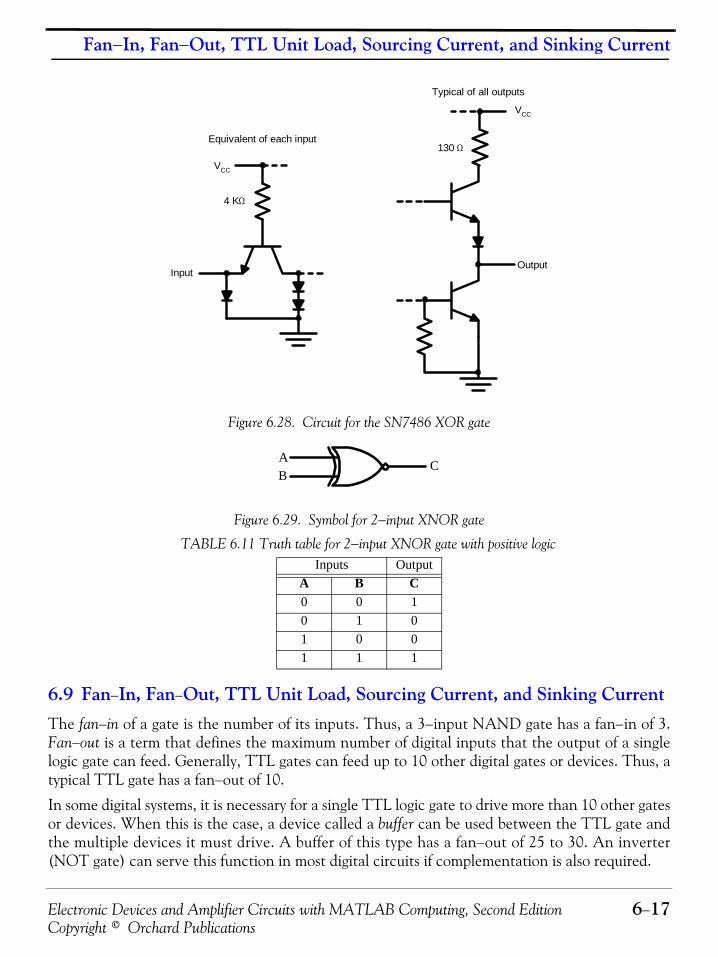
Electronic Devices and Amplifier Circuits with MATLAB Computing, Second Edition 6−17Copyright © Orchard Publications
Fan−In, Fan−Out, TTL Unit Load, Sourcing Current, and Sinking Current
Figure 6.28. Circuit for the SN7486 XOR gate
Figure 6.29. Symbol for 2−input XNOR gate
6.9 Fan−In, Fan−Out, TTL Unit Load, Sourcing Current, and Sinking CurrentThe fan−in of a gate is the number of its inputs. Thus, a 3−input NAND gate has a fan−in of 3.Fan−out is a term that defines the maximum number of digital inputs that the output of a singlelogic gate can feed. Generally, TTL gates can feed up to 10 other digital gates or devices. Thus, atypical TTL gate has a fan−out of 10.
In some digital systems, it is necessary for a single TTL logic gate to drive more than 10 other gatesor devices. When this is the case, a device called a buffer can be used between the TTL gate andthe multiple devices it must drive. A buffer of this type has a fan−out of 25 to 30. An inverter(NOT gate) can serve this function in most digital circuits if complementation is also required.
TABLE 6.11 Truth table for 2−input XNOR gate with positive logicInputs Output
A B C0 0 10 1 01 0 01 1 1
4 KΩ
VCC
130 Ω
VCC
InputOutput
Equivalent of each input
Typical of all outputs
CBA
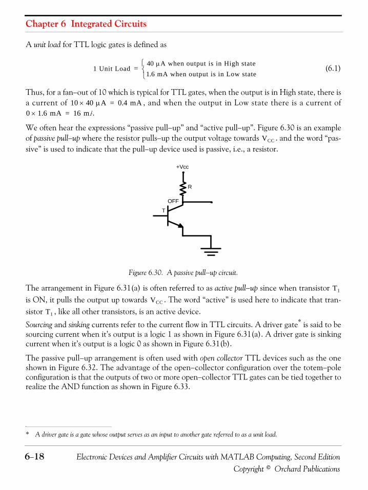
Chapter 6 Integrated Circuits
6−18 Electronic Devices and Amplifier Circuits with MATLAB Computing, Second EditionCopyright © Orchard Publications
A unit load for TTL logic gates is defined as
(6.1)
Thus, for a fan−out of 10 which is typical for TTL gates, when the output is in High state, there isa current of , and when the output in Low state there is a current of
.
We often hear the expressions “passive pull−up” and “active pull−up”. Figure 6.30 is an exampleof passive pull−up where the resistor pulls−up the output voltage towards . and the word “pas-sive” is used to indicate that the pull−up device used is passive, i.e., a resistor.
Figure 6.30. A passive pull−up circuit.
The arrangement in Figure 6.31(a) is often referred to as active pull−up since when transistor is ON, it pulls the output up towards . The word “active” is used here to indicate that tran-sistor , like all other transistors, is an active device.
Sourcing and sinking currents refer to the current flow in TTL circuits. A driver gate* is said to besourcing current when it’s output is a logic 1 as shown in Figure 6.31(a). A driver gate is sinkingcurrent when it’s output is a logic 0 as shown in Figure 6.31(b).
The passive pull−up arrangement is often used with open collector TTL devices such as the oneshown in Figure 6.32. The advantage of the open−collector configuration over the totem−poleconfiguration is that the outputs of two or more open−collector TTL gates can be tied together torealize the AND function as shown in Figure 6.33.
* A driver gate is a gate whose output serves as an input to another gate referred to as a unit load.
1 Unit Load40 μA when output is in High state1.6 mA when output is in Low state⎩
⎨⎧
=
10 40 μA× 0.4 mA=0 1.6 mA× 16 mA=
VCC
+Vcc
T
R
OFF
T1
VCC
T1

Electronic Devices and Amplifier Circuits with MATLAB Computing, Second Edition 6−19Copyright © Orchard Publications
Fan−In, Fan−Out, TTL Unit Load, Sourcing Current, and Sinking Current
Figure 6.31. Current sourcing and current sinking
Figure 6.32. Open−collector TTL configuration
+Vcc
T2
T1
+Vcc
T2
T1
Isource 0.4 mA=
10 unit loads( )
I ksin
10 unit loads( )
VOL 0.4 V=
I ksin 16 mA=
b( )a( )
D D
VOH 2.4 V=
+Vcc
+
-
4 Κ Ω
1 Κ Ω
1.6 Κ Ω
Input A
Output Y
T1
T3
T2
D1
Input B
D2
X (open collector point)
Chapter 6 Integrated Circuits
6−20 Electronic Devices and Amplifier Circuits with MATLAB Computing, Second EditionCopyright © Orchard Publications
Figure 6.33. Wired AND connection
To see why the outputs of two or more totem pole TTL gates should not be tied together forwired AND operation, let us consider the arrangement shown in Figure 6.34. With the collectorsof transistors and as shown, the current can be as high as which most likely willdamage transistors and , because per manufacturer’s specifications these transistors cansink only .
Figure 6.34. Improper wired AND connection
6.10 Data SheetsTable 6.12 lists some important parameters listed in the data sheets provided by the manufac-turer with typical values for a TTL 2−input NAND gate, SN7400. The reader is cautioned thatthese values are provided just for instructional purposes. For actual values, the manufacturer’slatest data sheet should always be used since the values change from time to time.
Item 1 in the table is self−explanatory, and we have already discussed Item 2. Therefore, we willcontinue with Items 3 through 13.
YX
Wired AND
T2 T4 I 55 mAT1 T4
16 mA
+Vcc
130 Ω
T2
T1
130 Ω
T4
T3
+Vcc
I
OFFON
ONOFF
Electronic Devices and Amplifier Circuits with MATLAB Computing, Second Edition 6−21Copyright © Orchard Publications
Data Sheets
3. The high level input voltage , also referred to as logical input voltage is the minimuminput voltage level that the IC device will recognize as a valid logical input as shown in Fig-ure 6.35.
4. The low level input voltage , also referred to as logical input voltage is the maximuminput voltage level that the IC device will recognize as a valid logical input as shown in Fig-ure 6.35.
TABLE 6.12 Typical parameters for TTL logic circuits provided by IC manufacturersParameter Conditions Min Typical Max Units
1 Supply voltage V
2 Input clamp voltage , , V
3 High Level Input Voltage
V
4 Low Level Input Voltage
V
5 High Level Output Voltage
, , V
6 Low Level Output Voltage
, , V
7 High Level Input Current
,
,
8 Low Level Input Current
,
9 Output Short Circuit Current
, ,
10 Low Level Supply Current
,
11 High Level Supply Current
,
12 Propagation Delay Time − High to Low Level
, , ns
13 Propagation Delay Time − Low to High Level
, , ns
VCC TA 25°C= 4.75 5.00 5.25
VIK
VCC Min= TA 25°C= IIN 12 mA–= 1.5–
VIH
VCC Min= 2.0
VIL
VCC Min= 0.8
VOH
VCC Min= VIL 0.8 V=
IOH 0.4 mA–=
2.4 3.4
VOL
VCC Min= VIH 2.0 V= IOL 16 mA= 0.2 0.4
IIH
VCC Max= VIN 2.4 V=
VCC Max= VIN 5.5 V=
40
1
μA
mA
IIL
VCC Max= VIN 0.4 V= 1.6– mA
IOS
VCC Max= VIN 0 V= VOUT 0= 18– 55– mA
ICCL
VCC Max= VIN 4.5 V= 2.4 4.4 mA
ICCH
VCC Max= VIN 0= 0.8 1.6 mA
tPHL
VCC 5.0 V= TA 25°C= RL 400 Ω=
CL 15 pF=
7 15
tPLH
VCC 5.0 V= TA 25°C= RL 400 Ω=
CL 15 pF=
11 22
VIH 11
VIL 00
Chapter 6 Integrated Circuits
6−22 Electronic Devices and Amplifier Circuits with MATLAB Computing, Second EditionCopyright © Orchard Publications
Figure 6.35. Valid logical and valid logical input regions for a typical IC gate
5. The high level output voltage , also referred to as logical output voltage is the mini-mum output voltage level that the IC device will recognize as a valid logical output.
6. The low level output voltage , also referred to as logical output voltage is the maximumoutput voltage level that the IC device will recognize as a valid logical output when a cur-rent of , representing a fan−out of , is sinked by transistor as indicated in Figure6.36.
Figure 6.36. Part of a typical NAND gate showing current sinking
nor ical log 0
Minimum ical 1log input
Logical 1 input region
Logical 0 input region
0.0 V
0.8 V
VCC 5.0 V=
2.0 V
5.0 V
Excluded regionNeither ical log 1
Maximum ical 0log input
VIH
VIL
1 0
VOH 11
VOL 00
16 mA 10 T2
+Vcc
130 Ω
T2
T1
Output 0.4 V=
I ksin 16 mA=

Electronic Devices and Amplifier Circuits with MATLAB Computing, Second Edition 6−23Copyright © Orchard Publications
Data Sheets
7.a. For a 2−input NAND gate, when the input voltage is , the maximum value of the sumof the currents furnished by the input lines should not be greater than for ten unitloads.
7.b. For a 2−input NAND gate, when the input voltage is , the maximum value of the sumof the currents furnished by the input lines should not be greater than for ten unitloads.
8. When the input voltage is low at , the maximum value of the current should notexceed where the minus sign indicates the direction of the current flow as shown inFigure 6.37 where for a logical input voltage the ten gates at the right side “source” (supply)
each, and the single gate on the left “sinks” (accepts) .
Figure 6.37. An illustration of the input current for a 2−input NAND gate
9. The output short−circuit current is the output current when the output is shorted toground as shown in Figure 6.38. The data sheet specifies an output short circuit current of
maximum. When transistor is ON, transistor is OFF, and the output voltage isgrounded, the resistor will act as a current limiter to limit the current in the range to
. Thus, the resistor provides short circuit protection.
10. The Low Level Supply Current is the current that the voltage supply must furnishwhen only one of the four TTL 2−input NAND gates within the IC SN7400 has its output atlogical . If two outputs are at logical , must furnish twice the amount of current spec-ified in the data sheet, that is, .
2.4 VIIH 40 μA
5.5 VIIH 1 mA
0.4 V IIL
1.6 mA–
01.6 mA– 1.6 10×– 16– mA=
VCC
⎭⎪⎪⎪⎪⎬⎪⎪⎪⎪⎫
16 mA
10gates
1.6 mA
1.6 mA
1.6 mA
IIL
IOS
55 mA T1 T2
18 mA55 mA
ICCL VCC
0 0 VCC
2 4.4× 8.8 mA=

Chapter 6 Integrated Circuits
6−24 Electronic Devices and Amplifier Circuits with MATLAB Computing, Second EditionCopyright © Orchard Publications
Figure 6.38. The definition of the output short−circuit current
11. The High Level Supply Current is the current that the voltage supply must furnishwhen only one of the four 2−input NAND gates within the IC SN7400 has its output at log-ical . If two outputs are at logical , must furnish twice the amount of current speci-fied in the data sheet, that is, .
12. The propagation delay time is the time required for a logical Input A or logical Input B to appear as logical at Output Y. A typical value is .
13. The propagation delay time is the time required for a logical Input A or logical Input B to appear as logical at Output Y. A typical value is .
6.11 Emitter Coupled Logic (ECL)
Let us consider the differential circuit shown in Figure 6.39, assume that transistors and are identical, and that . Then,
a. If , then , , and thus the differential outputis zero.
b. If , then , , and thus the differential output ispositive.
c. If , then , , and thus the differential output isnegative.
+Vcc
130 Ω
T2
T1
Ishort circuit
ICCH VCC
1 1 VCC
2 1.6× 3.2 mA=
tPHL 1 10 7 ns
tPLH 0 01 11 ns
T1 T2
RC1 RC2=
VB2 VB1= IC2 IC1= RC2IC2 RC1IC1= Vout2 Vout1=
VB2 VB1> IC2 IC1> RC2IC2 RC1IC1> Vout2 Vout1<
VB2 VB1< IC2 IC1< RC2IC2 RC1IC1< Vout2 Vout1>
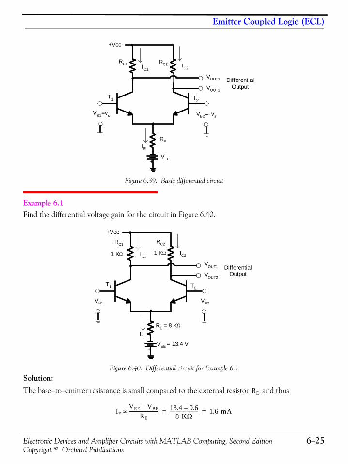
Electronic Devices and Amplifier Circuits with MATLAB Computing, Second Edition 6−25Copyright © Orchard Publications
Emitter Coupled Logic (ECL)
Figure 6.39. Basic differential circuit
Example 6.1 Find the differential voltage gain for the circuit in Figure 6.40.
Figure 6.40. Differential circuit for Example 6.1Solution:
The base−to−emitter resistance is small compared to the external resistor and thus
+Vcc
RC1
T2T1
+−
RC2
VEE
REIE
VB1=vs
IC1IC2
VOUT1
VOUT2
DifferentialOutput
VB2=−vs
DifferentialOutput
+Vcc
RC1
T2T1
+−
RC2
VEE = 13.4 V
RE = 8 KΩIE
VB1
IC1IC2
VOUT1
VOUT2
VB2
1 KΩ 1 KΩ
RE
IEVEE VBE–
RE-------------------------≈ 13.4 0.6–
8 KΩ------------------------ 1.6 mA= =
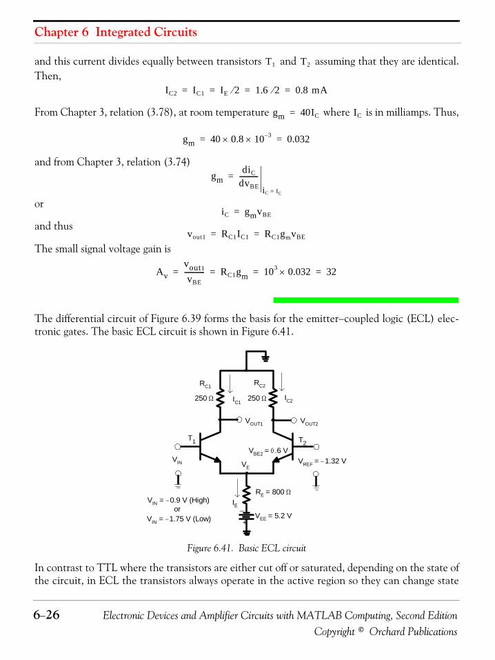
Chapter 6 Integrated Circuits
6−26 Electronic Devices and Amplifier Circuits with MATLAB Computing, Second EditionCopyright © Orchard Publications
and this current divides equally between transistors and assuming that they are identical.Then,
From Chapter 3, relation (3.78), at room temperature where is in milliamps. Thus,
and from Chapter 3, relation (3.74)
or
and thus
The small signal voltage gain is
The differential circuit of Figure 6.39 forms the basis for the emitter−coupled logic (ECL) elec-tronic gates. The basic ECL circuit is shown in Figure 6.41.
Figure 6.41. Basic ECL circuit
In contrast to TTL where the transistors are either cut off or saturated, depending on the state ofthe circuit, in ECL the transistors always operate in the active region so they can change state
T1 T2
IC2 IC1 IE 2⁄ 1.6 2⁄ 0.8 mA= = = =
gm 40IC= IC
gm 40 0.8× 10 3–× 0.032= =
gmdiC
dvBE-----------
iC IC=
=
iC gmvBE=
vout1 RC1IC1 RC1gmvBE= =
Avvout1
vBE------------ RC1gm 103 0.032× 32= = = =
VE
RC1
T2T1
+−
RC2
VEE = 5.2 V
RE = 800 ΩIE
VIN
IC1IC2
VOUT1 VOUT2
VREF = −1.32 V
250 Ω 250 Ω
VIN = −0.9 V (High)
VIN = −1.75 V (Low)or
VBE2 = 0 .6 V

Electronic Devices and Amplifier Circuits with MATLAB Computing, Second Edition 6−27Copyright © Orchard Publications
Emitter Coupled Logic (ECL)
very rapidly. We observe that with , the transistor is barely turned ON or barelyturned OFF and this allows a very rapid change of state from ON to OFF or vice versa. Thepropagation time for this arrangement is less than a nanosecond. However, there is a disadvantageand this is that the transistors are continually drawing current, which means the circuits requirehigh power, and this power is converted to energy in the form of unwanted heat.
In the circuit of Figure 6.41 the resistor values are approximate and for proper operation they mustbe very precise. The emitter current is almost constant since the base−to−emitter resistance ismuch smaller than the emitter resistor and this current flows through either transistor ortransistor depending on the value of while is held constant at with respect
to the ground. The condition is established as logical (High) and
as logical (Low). Also, and thus .
Let us now assume that , i.e., logical . Because , transistor does
not conduct and is essentially connected to the ground. To find when
(logical ), we must first find the current . We observe that
and
Therefore, with (logical ), we obtain and . Next,
let , i.e., logical . Because , transistor conducts hard, and transis-
tor is OFF, and is essentially connected to the ground. Therefore all current flows
through transistor and the collector current of this transistor is
and
Therefore, with (logical ), we obtain and . Weobserve that:
1. and are complements of each other.
2. The output voltage levels are not the same as input voltage levels, that is, the input levels are and and the outputs are and . However, the output levels can be
made comparable to the input levels by attaching two emitter followers to the outputs asshown in Figure 6.42.
VBE2 0.6 V= T2
IE
RE T2
T2 Vin VREF 1.32 V–
Vin 0.9 V–= 1 Vin 1.75 V–=
0 VBE2 VE+ VREF= VE 1.32– 0.6– 1.92 V–= =
Vin 1.75 V–= 0 VE 1.92 V–= T1
Vout1 Vout2 Vin 1.75 V–=
0 IC2
IC2 IE≈VE VEE–( )–
RE------------------------------ 1.92– 5.2–( )–
800------------------------------------ 4.1 mA= = =
Vout2 R– C2IC2 250– 4.1 103×× 1.03 V–= = =
Vin 1.75 V–= 0 Vout1 0 V= Vout2 1.03 V–=
Vin 0.9 V–= 1 VE 1.92 V–= T1
T2 Vout2
T1
IC1 IE≈VE VEE–( )–
RE------------------------------ 1.92– 5.2–( )–
800------------------------------------ 4.1 mA= = =
Vout1 R– C2IC2 250– 4.1 103×× 1.03 V–= = =
Vin 0.9 V–= 1 Vout1 1.03 V–= Vout2 0 V=
Vout1 Vout2
1.75 V– 0.9 V– 0 V 1.03 V–
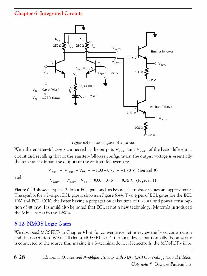
Chapter 6 Integrated Circuits
6−28 Electronic Devices and Amplifier Circuits with MATLAB Computing, Second EditionCopyright © Orchard Publications
Figure 6.42. The complete ECL circuit
With the emitter−followers connected at the outputs and of the basic differentialcircuit and recalling that in the emitter−follower configuration the output voltage is essentiallythe same as the input, the outputs at the emitter−followers are
and
Figure 6.43 shows a typical 2−input ECL gate and. as before, the resistor values are approximate.The symbol for a 2−input ECL gate is shown in Figure 6.44. Two types of ECL gates are the ECL10K and ECL 100K, the latter having a propagation delay time of and power consump-tion of . It should also be noted that ECL is not a new technology; Motorola introducedthe MECL series in the 1980’s.
6.12 NMOS Logic GatesWe discussed MOSFETs in Chapter 4 but, for convenience, let us review the basic constructionand their operation. We recall that a MOSFET is a 4−terminal device but normally the substrateis connected to the source thus making it a 3−terminal device. Henceforth, the MOSFET will be
VE
RC1
T2T1
+−
RC2
VEE = 5.2 V
RE = 800 ΩIE
VIN
IC1IC2
VOUT1
VREF = −1.32 V
250 Ω 250 Ω
VIN = −0.9 V (High)
VIN = −1.75 V (Low)or
VBE2 = 0 .6 V
V'OUT2
V'OUT1
VOUT2
100 Ω
100 Ω
−2 V
−2 V
0 .7 5 V
0 .7 5 V
+
+
−
−
Emitter follower
Emitter follower
V'out1 V'out2
Vout1 V'out1 VBE– 1.03– 0.75– 1.78 V ical 0log( )–= = =
Vout2 V'out2 VBE– 0.00 0.45– 0.75 V ical 1log( )–= = =
0.75 ns40 mW

Electronic Devices and Amplifier Circuits with MATLAB Computing, Second Edition 6−29Copyright © Orchard Publications
NMOS Logic Gates
shown as a 3−terminal block as in Figure 6.45.
Figure 6.43. Typical 2−input ECL gate
Figure 6.44. Symbol for ECL gate
Figure 6.45. Designations for n− and p−channel MOSFETS
An n−channel MOSFET or simply NMOS device, behaves like an open switch, as shown in Fig-ure 6.46, when . where and it is referred to as the threshold voltage.
Figure 6.46. Condition under which an NMOS device behaves as an open switch
VE
RC1
T3T2
+−
RC2
VEE = 5.2 V
RE = 800 ΩIE
IC1IC2
VREF = −1.32 V
250 Ω 250 Ω
VBE2 = 0 .6 V
Emitter follower
Emitter follower
A B
A+B
A+B
T1
A
BA+BA+B
G
D
B
S G
D
B
Sn channel– p channel–
N
D
G
S
P
D
G
S
VGS VT< VT 1.5 V=
N
D G
SVGS
+_
or
D
S
1010 Ω Open switch
SVGS VT<
VDD D
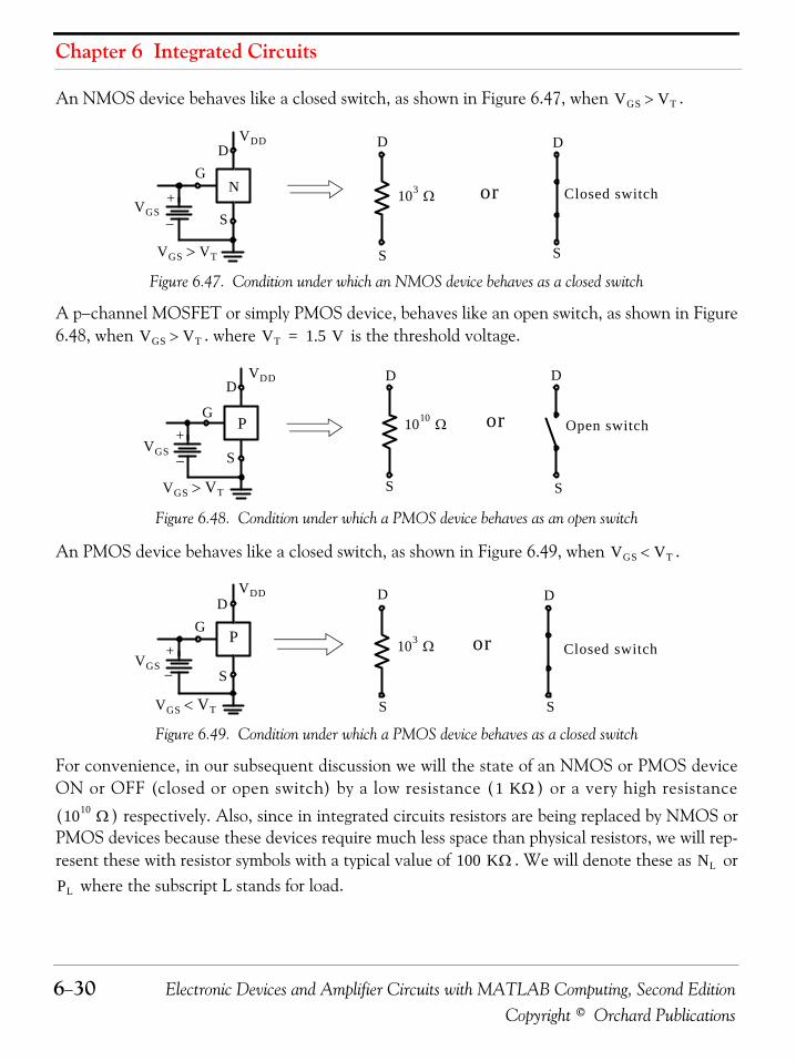
Chapter 6 Integrated Circuits
6−30 Electronic Devices and Amplifier Circuits with MATLAB Computing, Second EditionCopyright © Orchard Publications
An NMOS device behaves like a closed switch, as shown in Figure 6.47, when .
Figure 6.47. Condition under which an NMOS device behaves as a closed switch
A p−channel MOSFET or simply PMOS device, behaves like an open switch, as shown in Figure6.48, when . where is the threshold voltage.
Figure 6.48. Condition under which a PMOS device behaves as an open switch
An PMOS device behaves like a closed switch, as shown in Figure 6.49, when .
Figure 6.49. Condition under which a PMOS device behaves as a closed switch
For convenience, in our subsequent discussion we will the state of an NMOS or PMOS deviceON or OFF (closed or open switch) by a low resistance ( ) or a very high resistance
( ) respectively. Also, since in integrated circuits resistors are being replaced by NMOS orPMOS devices because these devices require much less space than physical resistors, we will rep-resent these with resistor symbols with a typical value of . We will denote these as or
where the subscript L stands for load.
VGS VT>
N
D G
S
VGS VT>
+_
or
D
S
103 Ω Closed switchVGS
VDD D
S
VGS VT> VT 1.5 V=
P
D
G
S
VGS VT>
+_
or
D
S
1010 Ω Open switch
D
S
VGS
VDD
VGS VT<
P
D G
S
VGS VT<
+_
or
D
S
103 Ω Closed switch
D
S
VDD
VGS
1 KΩ
1010 Ω
100 KΩ NL
PL
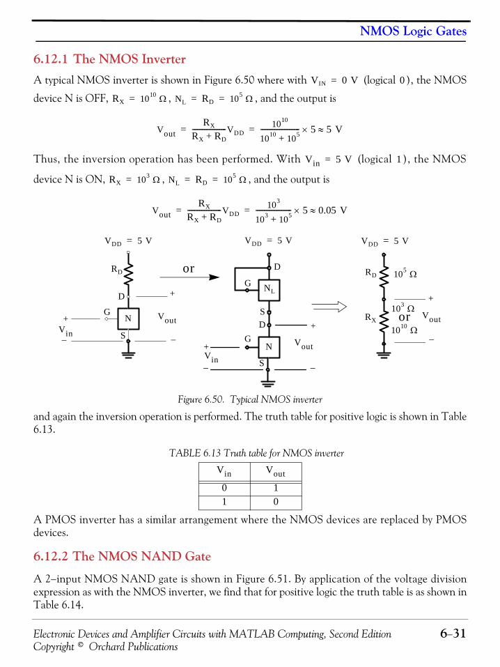
Electronic Devices and Amplifier Circuits with MATLAB Computing, Second Edition 6−31Copyright © Orchard Publications
NMOS Logic Gates
6.12.1 The NMOS InverterA typical NMOS inverter is shown in Figure 6.50 where with (logical ), the NMOS
device N is OFF, , , and the output is
Thus, the inversion operation has been performed. With (logical ), the NMOS
device N is ON, , , and the output is
Figure 6.50. Typical NMOS inverter
and again the inversion operation is performed. The truth table for positive logic is shown in Table6.13.
A PMOS inverter has a similar arrangement where the NMOS devices are replaced by PMOSdevices.
6.12.2 The NMOS NAND Gate
A 2−input NMOS NAND gate is shown in Figure 6.51. By application of the voltage divisionexpression as with the NMOS inverter, we find that for positive logic the truth table is as shown inTable 6.14.
TABLE 6.13 Truth table for NMOS inverter
0 11 0
VIN 0 V= 0
RX 1010 Ω= NL RD 105 Ω= =
VoutRX
RX RD+--------------------VDD
1010
1010 105+----------------------- 5× 5 V≈= =
Vin 5 V= 1
RX 103 Ω= NL RD 105 Ω= =
VoutRX
RX RD+--------------------VDD
103
103 105+--------------------- 5× 0.05 V≈= =
N
D
G
S
RD or
S
105 Ω
VDD 5 V=
Vin D
G
S
NL
D
G
VDD 5 V=
103 Ω+
_
Voutor
RD
RX
VDD 5 V=
+
_
Vout
+
_+
_Vin
+
_
Vout N
1010 Ω
Vin Vout

Chapter 6 Integrated Circuits
6−32 Electronic Devices and Amplifier Circuits with MATLAB Computing, Second EditionCopyright © Orchard Publications
Figure 6.51. 2−input NMOS NAND gate
6.12.3 The NMOS NOR Gate
A 2−input NMOS NOR gate is shown in Figure 6.52. By application of the voltage divisionexpression as with the NMOS NAND gate, we find that for positive logic the truth table is asshown in Table 6.15.
6.13 CMOS Logic GatesCMOS logic uses both NMOS and PMOS devices to form logic functions. CMOS technology isthe dominant semiconductor technology for the manufacturing of microprocessors, memoriesand application specific integrated circuits. The main advantage of CMOS over NMOS andbipolar technology is the much smaller power dissipation. Unlike NMOS or bipolar circuits, aCMOS circuit has almost no static power dissipation. Power is only dissipated in case the circuitactually switches. This allows to integrate many more CMOS gates on an IC than in NMOS orbipolar technology, resulting in much better performance.
TABLE 6.14 Truth table for 2−input NMOS NAND gateA B
0 0 10 1 11 0 11 1 0
S
105 Ω
N
D G
SA
NL
D
G
VDD 5 V=
103 Ω+
_
Vout
or1010 Ω
RD
VDD 5 V=
+
_
Vout D
G
B
or103 Ω
1010 Ω
N
S
+
+
_
_
Vout
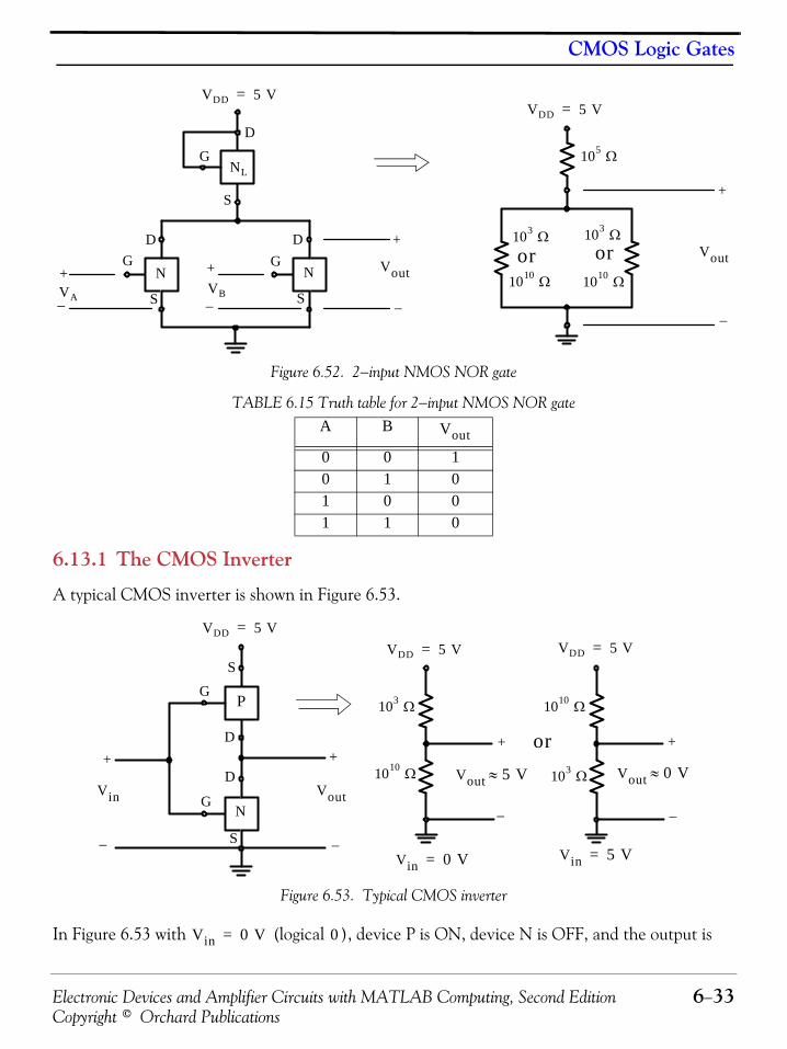
Electronic Devices and Amplifier Circuits with MATLAB Computing, Second Edition 6−33Copyright © Orchard Publications
CMOS Logic Gates
Figure 6.52. 2−input NMOS NOR gate
6.13.1 The CMOS Inverter
A typical CMOS inverter is shown in Figure 6.53.
Figure 6.53. Typical CMOS inverter
In Figure 6.53 with (logical ), device P is ON, device N is OFF, and the output is
TABLE 6.15 Truth table for 2−input NMOS NOR gateA B
0 0 10 1 01 0 01 1 0
S
105 Ω
N
D G
SVA
NL
D G
VDD 5 V=
103 Ω
+
_
Voutor1010 Ω
VDD 5 V=
+
_
Vout NVB
or103 Ω
1010 Ω G
D
S
+
_
+
_
Vout
N
D
S
or
VDD 5 V=
Vin
VDD 5 V=
1010 Ω+
_
Vout
P
D
S
G
G103 Ω
+
_
Vout 5 V≈
Vin 0 V=
1010 Ω
103 Ω
+
_
Vin 5 V=
VDD 5 V=
Vout 0 V≈
_
+
Vin 0 V= 0
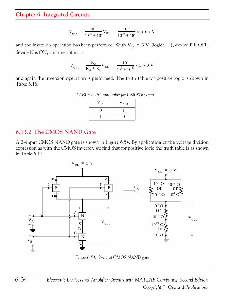
Chapter 6 Integrated Circuits
6−34 Electronic Devices and Amplifier Circuits with MATLAB Computing, Second EditionCopyright © Orchard Publications
and the inversion operation has been performed. With (logical ), device P is OFF,device N is ON, and the output is
and again the inversion operation is performed. The truth table for positive logic is shown inTable 6.16.
6.13.2 The CMOS NAND Gate
A 2−input CMOS NAND gate is shown in Figure 6.54. By application of the voltage divisionexpression as with the CMOS inverter, we find that for positive logic the truth table is as shownin Table 6.17.
Figure 6.54. 2−input CMOS NAND gate
TABLE 6.16 Truth table for CMOS inverter
0 11 0
Vout1010
1010 103+-----------------------VDD
1010
1010 103+----------------------- 5× 5 V≈= =
Vin 5 V= 1
VoutRX
RX RD+--------------------VDD
103
103 1010+----------------------- 5× 0 V≈= =
Vin Vout
VDD 5 V=
D G
SVA
+
_
Vout
N
D G
S
D
G S
P G
D
VDD 5 V=
103 Ωor
1010 Ωor
1010 Ω
103 Ω
103 Ωor
1010 Ω
SVB
_
_
_
+
+ +
Vout
N
P
or1010 Ω
103 Ω

Electronic Devices and Amplifier Circuits with MATLAB Computing, Second Edition 6−35Copyright © Orchard Publications
Buffers, Tri−State Devices, and Data Buses
6.13.3 The CMOS NOR Gate
A 2−input CMOS NOR gate is shown in Figure 6.55. By application of the voltage divisionexpression as with the CMOS inverter, we find that for positive logic the truth table is as shown inTable 6.18.
Figure 6.55. 2−input CMOS NOR gate
6.14 Buffers, Tri−State Devices, and Data BusesIn certain applications, the output of a logic circuit needs to be buffered. A buffer or line driver isnormally used to change (amplify) the voltage level at the output of a logic circuit as shown in Fig-ure 6.56.
TABLE 6.17 Truth table for 2−input CMOS NAND gate
0 0 10 1 11 0 11 1 0
TABLE 6.18 Truth table for 2−input CMOS NOR gate
0 0 10 1 01 0 01 1 0
VA VB Vout
D
G
+
Vout
P
D
G
VDD 5 V=
103 Ωor
1010 Ω
or103 Ω
1010 Ω
103 Ωor
1010 Ω
103 Ωor
1010 Ω
N G
N G
D D
S
S
S S
VDD 5 V=+
+
PVA
VB
+
Vout
VA VB Vout
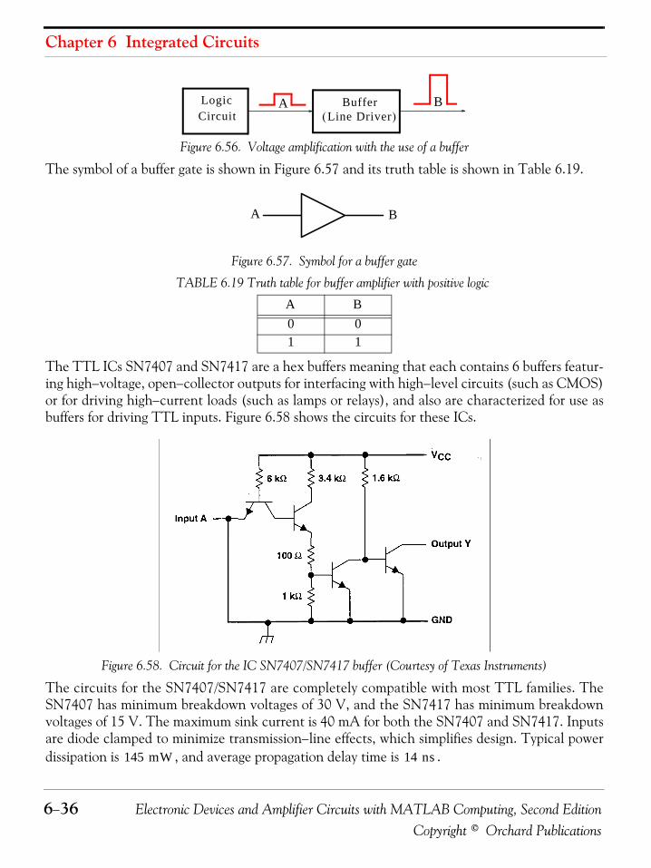
Chapter 6 Integrated Circuits
6−36 Electronic Devices and Amplifier Circuits with MATLAB Computing, Second EditionCopyright © Orchard Publications
Figure 6.56. Voltage amplification with the use of a buffer
The symbol of a buffer gate is shown in Figure 6.57 and its truth table is shown in Table 6.19.
Figure 6.57. Symbol for a buffer gate
The TTL ICs SN7407 and SN7417 are a hex buffers meaning that each contains 6 buffers featur-ing high−voltage, open−collector outputs for interfacing with high−level circuits (such as CMOS)or for driving high−current loads (such as lamps or relays), and also are characterized for use asbuffers for driving TTL inputs. Figure 6.58 shows the circuits for these ICs.
Figure 6.58. Circuit for the IC SN7407/SN7417 buffer (Courtesy of Texas Instruments)
The circuits for the SN7407/SN7417 are completely compatible with most TTL families. TheSN7407 has minimum breakdown voltages of 30 V, and the SN7417 has minimum breakdownvoltages of 15 V. The maximum sink current is 40 mA for both the SN7407 and SN7417. Inputsare diode clamped to minimize transmission−line effects, which simplifies design. Typical powerdissipation is , and average propagation delay time is .
TABLE 6.19 Truth table for buffer amplifier with positive logic
0 01 1
LogicCircuit
BufferLine Driver( )
A B
A B
A B
145 mW 14 ns

Electronic Devices and Amplifier Circuits with MATLAB Computing, Second Edition 6−37Copyright © Orchard Publications
Buffers, Tri−State Devices, and Data Buses
Other examples of buffered gates are the TTL SN7406/SN7416 Hex Inverter buffers with open−collector high−voltage outputs, the SN7428 quad 2−input positive−nor buffers, and the SN7440dual−four input positive−NAND buffers.
Some other ICs are tri−stated buffers or gates. The output of these devices can assume three states,logic 0, logic 1, and High−Z (high impedance), that is, an open circuit. Figure 6.59 shows the sym-bols for ICs SN74125 and SN74126 quad bus buffers with 3−state outputs.
Figure 6.59. Symbols for the TTL SN74125 and SN74126 devices
The output of the SN74125 device is disabled when is High, and the output of the SN74126 isdisabled when is Low. The truth table for the SN74125 device is shown in Table 6.20.
Figure 6.60 shows the symbol for the TTL SN74366 hex tri−state inverting buffer, and Table 6.21is the truth table for that device.
Figure 6.60. Symbol for the SN74366 hex tri−state inverting buffer
TABLE 6.20 Truth table for the SN74125 3−state bufferA B
0 0 00 1 11 0 High Z1 1 High Z
TABLE 6.21 Truth table for the TTL SN74125 3−state bufferA B
0 0 10 1 01 0 High Z1 1 High Z
G
A B A
G
B
SN74125 SN74126
GG
G
A
G
B
G
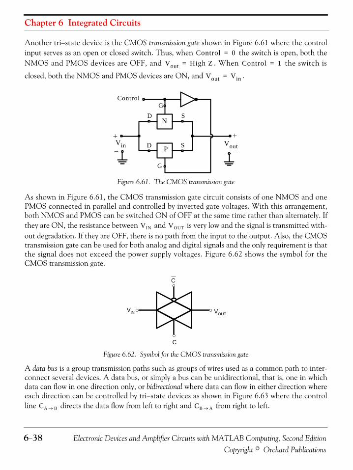
Chapter 6 Integrated Circuits
6−38 Electronic Devices and Amplifier Circuits with MATLAB Computing, Second EditionCopyright © Orchard Publications
Another tri−state device is the CMOS transmission gate shown in Figure 6.61 where the controlinput serves as an open or closed switch. Thus, when the switch is open, both theNMOS and PMOS devices are OFF, and . When the switch is
closed, both the NMOS and PMOS devices are ON, and .
Figure 6.61. The CMOS transmission gate
As shown in Figure 6.61, the CMOS transmission gate circuit consists of one NMOS and onePMOS connected in parallel and controlled by inverted gate voltages. With this arrangement,both NMOS and PMOS can be switched ON of OFF at the same time rather than alternately. Ifthey are ON, the resistance between and is very low and the signal is transmitted with-out degradation. If they are OFF, there is no path from the input to the output. Also, the CMOStransmission gate can be used for both analog and digital signals and the only requirement is thatthe signal does not exceed the power supply voltages. Figure 6.62 shows the symbol for theCMOS transmission gate.
Figure 6.62. Symbol for the CMOS transmission gate
A data bus is a group transmission paths such as groups of wires used as a common path to inter-connect several devices. A data bus, or simply a bus can be unidirectional, that is, one in whichdata can flow in one direction only, or bidirectional where data can flow in either direction whereeach direction can be controlled by tri−state devices as shown in Figure 6.63 where the controlline directs the data flow from left to right and from right to left.
Control 0=
Vout High Z= Control 1=
Vout Vin=
N
P
Control
Vin VoutD
G
G
D S
S
VIN VOUT
C
VIN VOUT
C
CA B→ CB A→

Electronic Devices and Amplifier Circuits with MATLAB Computing, Second Edition 6−39Copyright © Orchard Publications
Present and Future Technologies
Figure 6.63. Typical bidirectional bus
6.15 Present and Future TechnologiesThe IC devices that we described in previous sections of this chapter have been around for overforty years. Since speed and low−power consumption are the most desirable characteristics, justabout all of these devices have been replaced with newer devices even though the ICs that wedescribed are still in use by experimenters and laboratory work in colleges and universities.
In Chapter 3, we saw how the addition of a Schottky diode can be used to prevent transistor satu-ration as shown in Figure 6.64.
Figure 6.64. Bipolar NPN transistor with Schottky diode and its representation as Schottky transistor
To achieve low−power consumption, the resistances are considerably higher in the upgraded ver-sions of the TTL family and the ICs are identified with the LS designation which stands for Low−power Schottky device. Thus, the Low−power Schottky 2−input NAND gate is identified asSN74LS00 whose internal construction is shown in Figure 6.65.
A1
A2
An
B1
B2
Bn
CA B→ CB A→
E
C
B
diodeSchottky
C
E
B
Schottkytransistor
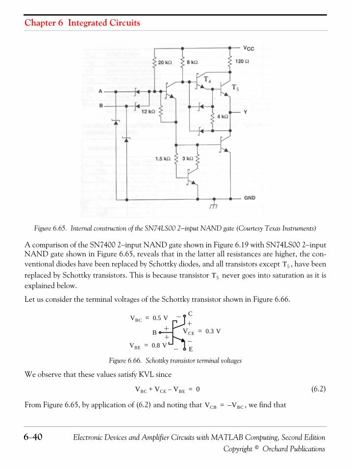
Chapter 6 Integrated Circuits
6−40 Electronic Devices and Amplifier Circuits with MATLAB Computing, Second EditionCopyright © Orchard Publications
Figure 6.65. Internal construction of the SN74LS00 2−input NAND gate (Courtesy Texas Instruments)
A comparison of the SN7400 2−input NAND gate shown in Figure 6.19 with SN74LS00 2−inputNAND gate shown in Figure 6.65, reveals that in the latter all resistances are higher, the con-ventional diodes have been replaced by Schottky diodes, and all transistors except , have beenreplaced by Schottky transistors. This is because transistor never goes into saturation as it isexplained below.
Let us consider the terminal voltages of the Schottky transistor shown in Figure 6.66.
Figure 6.66. Schottky transistor terminal voltages
We observe that these values satisfy KVL since
(6.2)
From Figure 6.65, by application of (6.2) and noting that , we find that
T5
T4
T5
T5
C
E
B
VBC 0.5 V=
VCE 0.3 V=
VBE 0.8 V=
VBC VCE VBE–+ 0=
VCB VBC–=
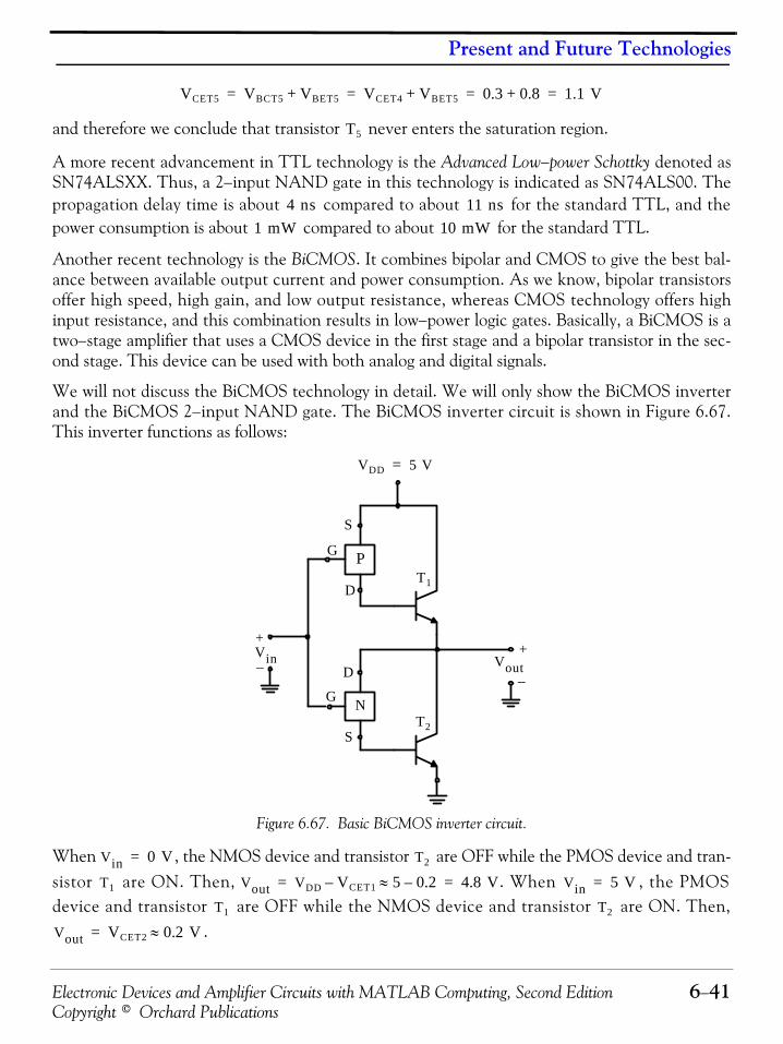
Electronic Devices and Amplifier Circuits with MATLAB Computing, Second Edition 6−41Copyright © Orchard Publications
Present and Future Technologies
and therefore we conclude that transistor never enters the saturation region.
A more recent advancement in TTL technology is the Advanced Low−power Schottky denoted asSN74ALSXX. Thus, a 2−input NAND gate in this technology is indicated as SN74ALS00. Thepropagation delay time is about compared to about for the standard TTL, and thepower consumption is about compared to about for the standard TTL.
Another recent technology is the BiCMOS. It combines bipolar and CMOS to give the best bal-ance between available output current and power consumption. As we know, bipolar transistorsoffer high speed, high gain, and low output resistance, whereas CMOS technology offers highinput resistance, and this combination results in low−power logic gates. Basically, a BiCMOS is atwo−stage amplifier that uses a CMOS device in the first stage and a bipolar transistor in the sec-ond stage. This device can be used with both analog and digital signals.
We will not discuss the BiCMOS technology in detail. We will only show the BiCMOS inverterand the BiCMOS 2−input NAND gate. The BiCMOS inverter circuit is shown in Figure 6.67.This inverter functions as follows:
Figure 6.67. Basic BiCMOS inverter circuit.
When , the NMOS device and transistor are OFF while the PMOS device and tran-sistor are ON. Then, . When , the PMOSdevice and transistor are OFF while the NMOS device and transistor are ON. Then,
.
VCET5 VBCT5 VBET5+ VCET4 VBET5+ 0.3 0.8+ 1.1 V= = = =
T5
4 ns 11 ns1 mW 10 mW
N
D
S
VDD 5 V=
Vin+
_Vout
P
D
S
G
G
T2
T1
+
_
Vin 0 V= T2
T1 Vout VDD VCET1– 5 0.2–≈ 4.8 V= = Vin 5 V=
T1 T2
Vout VCET2 0.2 V≈=

Chapter 6 Integrated Circuits
6−42 Electronic Devices and Amplifier Circuits with MATLAB Computing, Second EditionCopyright © Orchard Publications
The BiCMOS 2−input NAND gate has the same arrangement as the 2−input CMOS NANDgate with the addition of two NPN transistors at the outputs of the NMOS and PMOS devices asshown in Figure 6.68.
Figure 6.68. The basic BiCMOS NAND gate
As we mentioned in Chapter 3, gallium arsenide (GaAs) is the fastest technology with propagationdelay times about and even though prices for these devices have fallen considerably duringthe last few years, the cost is still very high in comparison with other IC families.
Undoubtedly, faster and with lower power consumption devices will emerge in the future. Theinterested reader is urged to check occasionally the Internet for new products developed byTexas Instruments, Motorola, National Semiconductor, Fairchild, and other IC manufacturersfor new products.
N
D
S
+
Vout N
D
G
S
P
D
G S
P G
D
VDD 5 V=
S
R
+
+
_
_
_
VA
VB
G
R
T1
T2
20 ps
Electronic Devices and Amplifier Circuits with MATLAB Computing, Second Edition 6−43Copyright © Orchard Publications
Summary
6.16 Summary• Electronic logic gates are used extensively in digital systems and are manufactured as integrated
circuits (IC’s). The basic logic gates are the inverter or NOT gate, the AND gate, and the ORgate, and these perform the complementation, ANDing, and ORing operations respectively.
• Four other logic gates, known as NAND, NOR, Exclusive OR (XOR), and Exclusive NOR(XNOR), are derivatives of the basic AND and OR gates. However, AND and OR gates con-sist of NAND and NOR gates respectively, followed by an Inverter.
• Generally, an uncomplemented variable represents a logical , also referred to as the true con-dition, and when that variable is complemented, it represents a logical , also referred to as thefalse condition. Thus, if (true), it follows that (false).
• Integrated circuit manufacturers assign the letter H (High) to the level and the letter L(Low) to the ground level. With the H and L assignments, the logic circuitry designer has theoption of assigning a logical to H and logical to L, or logical to H and logical to L. Theformer convention is known as positive logic, and the latter as negative logic.
• The Inverter performs the complementation operation. Thus if the input is the output willbe and vice versa. The TTL SN7404 Hex Inverter is a popular transistor−transistor logic(TTL) IC device. All SN74 series devices are TTL devices. The newer SN74ALS04 device isfaster and consumes less power. ALS stands for Advanced Low power Schottky transistor.
• The output of an AND gate is logical (true) only when all inputs are logical . The earlierTTL SN7408 Quad 2−input AND gate has been superseded with the SN74ALS08 device.
• The output of an OR gate is logical (true) whenever one or more of its inputs are logical .The earlier SN7432 Quad 2−input OR gate has been superseded with the SN74ALS32 device.
• The output of an NAND gate is logical (false) only when all inputs are logical . The earlierSN7400 Quad 2−input NAND gate has been superseded with the SN74ALS00 device.
• The input clamp voltage denoted as is the maximum negative voltage that may be applied atthe input terminals of a typical TTL gate without damaging the IC. To insure that this value isnot exceeded, diodes are included at the inputs of gates.
• The output of an NOR gate is logical (true) only when all inputs are logical (false). TheSN7402 Quad 2−input NOR gate has been superseded with the SN74ALS02 device.
• The exclusive−OR (XOR) logic gate has two inputs and one output. The output of an exclu-sive−OR gate is logical (true) when only one of the inputs, but not both, is logical . TheSN7486 XOR gate has been superseded with the SN74ALS86 device.
• The exclusive−NOR (XNOR) logic gate has two inputs and one output. The output of aXNOR gate is logical (true) only when the inputs are the same, that is, both logical or
10
A 1= A 0=
5 volt
1 0 0 1
AA
1 1
1 1
0 1
VIK
1 0
1 1
1 0

Chapter 6 Integrated Circuits
6−44 Electronic Devices and Amplifier Circuits with MATLAB Computing, Second EditionCopyright © Orchard Publications
both logical . For this reason, the XNOR gate is also known as equivalence gate. There is noIC XNOR gate in the TTL family but one can be formed with an XOR gate (SN7486) fol-lowed by an inverter (SN7404). We can also implement the XNOR function using theSN7486 IC with negative logic.
• The fan−in of a gate is the number of its inputs. Thus, a 3−input NAND gate has a fan−in of 3.
• Fan−out is a term that defines the maximum number of digital inputs that the output of a sin-gle logic gate can feed. Generally, TTL gates can feed up to 10 other digital gates or devices.Thus, a typical TTL gate has a fan−out of 10.
• A buffer can be used when it becomes necessary for a single TTL logic gate to drive more than10 other gates or devices. A typical buffer has a fan−out of 25 to 30. An inverter (NOT gate)can serve this function in most digital circuits if complementation is also required.
• For TTL logic gates, one unit load is defined as when the output is in High state, and when the output is in Low state.
• Passive pull−up refers to the condition where a resistor pulls−up the output voltage towards.
• Active pull−up refers to the condition where a transistor rather than a resistor is used to pull−up the output voltage towards .
• Sourcing and sinking currents refer to the current flow in TTL circuits. A driver gate is said tobe sourcing current when it’s output is High. A driver gate is sinking current when it’s outputis Low.
• Totem−pole configuration refers to the arrangement where at the output stage of a TTL gateone transistor is stacked on top of another and their operation is complementary, that is,when one transistor is ON the other transistor is OFF.
• Some TTL logic gates are designed with the collector of transistor at the output stage uncon-nected and are referred to as open collector TTL devices. The advantage of the open−collec-tor configuration over the totem−pole configuration is that the outputs of two or more open−collector TTL gates can be tied together to realize the AND function. This arrangement isreferred to as wired−AND operation. The passive pull−up arrangement is often used with opencollector TTL devices.
• Totem pole TTL gates should not be tied together for wired AND operation.
• The data sheets provided by IC device manufacturers contain very important parameters thatdesigners must take into consideration.
• Besides the TTL, the emitter−coupled logic (ECL) is another logic family employing bipolartransistors, and with the exception of gallium arsenide technology, is the fastest logic family.
1
40 μA1.6 mA
VCC
VCC
Electronic Devices and Amplifier Circuits with MATLAB Computing, Second Edition 6−45Copyright © Orchard Publications
Summary
• In contrast to TTL where the transistors are either cut off or saturated, depending on the stateof the circuit, in ECL the transistors always operate in the active region so they can changestate very rapidly. The basic ECL circuit is essentially a differential amplifier.
• The ECL gate provides two outputs, one which implements the OR function, and the otherimplements the NOR function.
• Two types of ECL gates are the ECL 10K and ECL 100K, the latter having a propagation delaytime of and power consumption of . It should also be noted that ECL is not anew technology; Motorola introduced the MECL series in the 1980’s.
• The earlier NMOS and PMOS logic gates have now been superseded by CMOS logic gates.CMOS logic uses both NMOS and PMOS devices to form logic functions. CMOS technologyis the dominant semiconductor technology for the manufacturing of microprocessors, memoriesand application specific integrated circuits. The main advantage of CMOS over NMOS andbipolar technology is the much smaller power dissipation.
• A buffer or line driver is normally used to change (amplify) the voltage level at the output of alogic circuit.
• Some other ICs are tri−stated buffers or gates. The output of these devices can assume threestates, logic 0, logic 1, and High−Z (high impedance).
• The CMOS transmission gate is another tri−state device where the control input serves as anopen or closed switch.
• A data bus is a group transmission paths such as groups of wires used as a common path tointerconnect several devices. A data bus, or simply a bus can be unidirectional, that is, one inwhich data can flow in one direction only, or bidirectional where data can flow in either direc-tion where each direction can be controlled by tri−state devices.
• A more recent advancement in TTL technology is the Advanced Low−power Schottky denotedas ALS. Thus, a 2−input NAND gate in this technology is indicated as SN74ALS00. The prop-agation delay time is about compared to about for the standard TTL, and thepower consumption is about compared to about for the standard TTL.
• The BiCMOS technology combines bipolar and CMOS to give the best balance between avail-able output current and power consumption. Bipolar transistors offer high speed, high gain, andlow output resistance, whereas CMOS technology offers high input resistance, and this combi-nation results in low−power logic gates. Basically, a BiCMOS is a two−stage amplifier that usesa CMOS device in the first stage and a bipolar transistor in the second stage. This device canbe used with both analog and digital signals.
• Gallium arsenide (GaAs) still remains the fastest technology with propagation delay times about and even though prices for these devices have fallen considerably during the last few
years, the cost is still very high in comparison with other IC families.
0.75 ns 40 mW
4 ns 11 ns1 mW 10 mW
20 ps
Chapter 6 Integrated Circuits
6−46 Electronic Devices and Amplifier Circuits with MATLAB Computing, Second EditionCopyright © Orchard Publications
6.17 Exercises1. The circuit below is known as Resistor Logic (RL) gate.
a. Write the truth table for the input combinations of and with respect to theground.
b. State the conditions under which this circuit can be classified as an AND gate.
c. State the conditions under which this circuit can be classified as an OR gate.
d. State some of the deficiencies of this circuit when used as a logic gate.
2. The circuit below is known as Diode Logic (DL) gate.
Write the truth table for the input combinations of and with respect to the ground.Which type of logic gate does this circuit represent?
3. The circuit below is another form of a Diode Logic (DL) gate.
Write the truth table for the input combinations of and with respect to the ground.Which type of logic gate does this circuit represent?
VoutV2
V1
1 KΩ
1 KΩ
1 KΩ
0 V 5 V
Vout15 KΩ
5 V
V1
V2
0 V 3 V
Vout1 KΩ
V1
V2
0 V 5 V

Electronic Devices and Amplifier Circuits with MATLAB Computing, Second Edition 6−47Copyright © Orchard Publications
Exercises
4. The circuit below is a 3−input Resistor−Transistor Logic (RTL) gate.
Write the truth table for the input combinations of and with respect to the ground.Which type of logic gate does this circuit represent?
5. For the circuit below find and when each of through assumes the values of
and with respect to the ground.
6. For the circuit of Exercise 5, derive an expression for High level when the driving gatehas a fan−out of 2. Hint: Start with an equivalent circuit.
7. The circuit below is a 3−input Diode−Transistor Logic (DTL) gate.
750 Ω
750 Ω
750 Ω
1 KΩ
T1
5 V
T2
T3
V1
V2
V3
Vout
0 V 5 V
Vout1 Vout2 V1 V4
0 V 5 V
V1
V2
V3
750 Ω
750 Ω
750 Ω
750 Ω 1 KΩ
T1
T2
T41 KΩ
5 V
5 V
T3
V4
Vout1
Vout2
Vout1

Chapter 6 Integrated Circuits
6−48 Electronic Devices and Amplifier Circuits with MATLAB Computing, Second EditionCopyright © Orchard Publications
Write the truth table for the input combinations of and with respect to the ground.Which type of logic gate does this circuit represent?
8. It is known that the inverter circuit shown below has the value minimum. Calculatethe levels of the output voltage when the levels of the input voltage are 0 and 12
volts. You may first assume that to obtain approximate values and then
assume that for exact values.
D5D4
D3
D2
D1
V1
V2
V3
Vout
R3
VCC 5 V=
R2R1 2 KΩ 2 KΩ
20 KΩ
0 V 5 V
hFE 30=
vout vin
vout sat( ) 0 V=
vout sat( ) 0.2 V=
vout
vin
RC
VCC 12 V=
R2
R1
100
2.2 KΩ
15 KΩ
KΩ
VBB 12– V=

Electronic Devices and Amplifier Circuits with MATLAB Computing, Second Edition 6−49Copyright © Orchard Publications
Solutions to End−of−Chapter Exercises
6.18 Solutions to End−of−Chapter Exercises1.
a. With , . With , and , is in parallel with
and by the voltage division expression
With , and , is in parallel with and by the voltage divisionexpression
With , we apply the principle of superposition and we find that
With these values we construct the truth table below.
b. This circuit can be classified as an AND gate if
c. This circuit can be classified as an OR gate if
d. This circuit is not practical for use as a logic gate because if more than two inputs exist, moredifferent output levels result. Moreover, there is no compatibility between the input andoutput levels. With the above arrangement for instance, with the output is
and if this output becomes the input of another gate shown below as Gate 3,
the outputs drop to as shown in parentheses.
0 V 0 V 0 V0 V 5 V 1.67 V5 V 0 V 1.67 V5 V 5 V 3.34 V
VoutV2
V1
1 KΩ
1 KΩ
1 KΩ
V1 V2 0 V= = Vout 0 V= V1 0 V= V2 5 V= R1
R3
Voutt V1 0 V=
R1 R3||R2 R1 R3||+----------------------------- V2⋅ 0.5 KΩ
1 KΩ 0.5 KΩ+------------------------------------- 5 V⋅ 1.67 V= = =
V1 5 V= V2 0 V= R2 R3
Vout V2 0 V=
R2 R3||R1 R2 R3||+----------------------------- V1⋅ 0.5 KΩ
1 KΩ 0.5 KΩ+------------------------------------- 5 V⋅ 1.67 V= = =
V1 V2 5 V= =
Vout V1 V2 5 V= =Vout V1 0 V=
Vout V2 0 V=+ 1.67 1.67+ 3.34 V= = =
V1 V2 Vout
Vout 3.34 V≥
Vout 1.67 V≥
V1 V2 5 V= =
Vout 3.34 V=
2.72 V
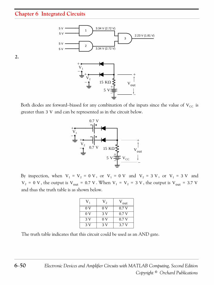
Chapter 6 Integrated Circuits
6−50 Electronic Devices and Amplifier Circuits with MATLAB Computing, Second EditionCopyright © Orchard Publications
2.
Both diodes are forward−biased for any combination of the inputs since the value of isgreater than and can be represented as in the circuit below.
By inspection, when , or and , or and, the output is . When , the output is
and thus the truth table is as shown below.
The truth table indicates that this circuit could be used as an AND gate.
0 V 0 V 0.7 V0 V 3 V 0.7 V3 V 0 V 0.7 V3 V 3 V 3.7 V
3
2
1
5 V
5 V
5 V
5 V
2.23 V (1.81 V)
3.34 V (2.72 V)
3.34 V (2.72 V)
Vout15 KΩ
5 V
V1
V2
VCC
3 V
Vout15 KΩ
5 V
V1
V2
VCC
0.7 V
0.7 V
V1 V2 0 V= = V1 0 V= V2 3 V= V1 3 V=
V2 0 V= Vout 0.7 V= V1 V2 3 V= = Vout 3.7 V=
V1 V2 Vout

Electronic Devices and Amplifier Circuits with MATLAB Computing, Second Edition 6−51Copyright © Orchard Publications
Solutions to End−of−Chapter Exercises
3.
By inspection, when , the output is . When and
, or and , or , one or both diodes conduct andthe output is and thus the truth table is as shown below.
The truth table indicates that this circuit could be used as an OR gate.
4.
By inspection, when , none of the three transistors conduct and thus. When one or more of the input voltages is one or more of the transistors will
saturate and the output will be . The truth table is as shown below and thusthis circuit behaves as a 3−input NOR gate.
0 V 0 V 0 V0 V 5 V 4.3 V5 V 0 V 4.3 V5 V 5 V 4.3 V
Vout1 KΩ
V1
V2
V1 V2 0 V= = Vout 0 V= V1 0 V=
V2 5 V= V1 5 V= V2 0 V= V1 V2 5 V= =
Vout 5.0 0.7– 4.3 V= =
V1 V2 Vout
750 Ω
750 Ω
750 Ω
1 KΩ
T1
5 V
T2
T3
V1
V2
V3
Vout
V1 V2 V3 0 V= = =
Vout 5 V= 5 V
Vout 0.2 V 0 V≈=

Chapter 6 Integrated Circuits
6−52 Electronic Devices and Amplifier Circuits with MATLAB Computing, Second EditionCopyright © Orchard Publications
5.
This circuit is a 2−input NOR gate with fan−out of 1. We recall that fan−out is the number ofgate inputs that can be driven by a single gate output. Thus, in the circuit above the output ofthe first 2−input NOR gate drives (is connected to) one of the inputs of the second 2−inputNOR gate. By inspection, when and , or and , or
, one of both transistors and conduct and thus .
When and , .
Next, let us examine the case where . Under this condition because current flows through the at the base of transistor which now conducts,and and . We can now find that current from the equivalent circuit below.
Inputs Output
0 V 0 V 0 V 5 V0 V 0 V 5 V 0 V0 V 5 V 0 V 0 V0 V 5 V 5 V 0 V5 V 0 V 0 V 0 V5 V 0 V 5 V 0 V5 V 5 V 0 V 0 V5 V 5 V 5 V 0 V
V1 V2 V3 Vout
V1
V2
V3
750 Ω
750 Ω
750 Ω
750 Ω 1 KΩ
T1
T2
T41 KΩ
5 V
5 V
T3
V4
Vout1
Vout2
V1 0 V= V2 5 V= V1 5 V= V2 0 V=
V1 V2 5 V= = T1 T2 Vout1 0.2 V 0 V≈=
V3 0 V= Vout1 0 V= Vout2 5 V=
V1 V2 5 V= = Vout1 5 V<
750 Ω T4
VBET4 0.7 V=

Electronic Devices and Amplifier Circuits with MATLAB Computing, Second Edition 6−53Copyright © Orchard Publications
Solutions to End−of−Chapter Exercises
The actual value of is minus the voltage drop across the resistor. Thus,
We see then that by connecting one input of a gate to the output of another gate causes thehigh level to decrease from its open circuit value of to the value of .
6.For a fan−out of 2, the equivalent circuit is as shown in Figure (a) below and its Theveninequivalent is as shown in Figure (b).
From Figure (b)
and
The equivalent circuit of Figure (a) can be extended to the situation where there are N gatesdriven by one output of a gate, that is a fan−out of N, by replacing the resistance by
. Then,
1 KΩ
750 Ω
5 V
0.7 V
I
I 5 0.7–1000 750+--------------------------- 4.3
1750------------ 2.46 mA= = =
Vout1 5 V 1 KΩ
Vout1 5 103 2.46 10 3–××– 2.54 V= =
5 V 2.54 V
1 KΩ 750 Ω 750 Ω 1 KΩ 750 2⁄ Ω
5 V 5 V0.7 V 0.7 V 0.7 V
b( )a( )
I
I 5 0.7–1000 750 2⁄+---------------------------------- 4.3
1000 750 2⁄+----------------------------------= =
Vout1 5 10001000 750 2⁄+----------------------------------4.3– 1.87 V= =
750 2⁄750 N⁄
Vout1 5 10001000 750 N⁄+----------------------------------4.3–=

Chapter 6 Integrated Circuits
6−54 Electronic Devices and Amplifier Circuits with MATLAB Computing, Second EditionCopyright © Orchard Publications
Note: RTL is no longer used as a logic family. It is one of the earlier families employed yearsago with a maximum fan−out of 5 and fan−in of 4.
7.
With one or more of the inputs , , or at , the given circuit becomes as shownbelow where the is assumed to be the output of a previous logic gate with logical .
With , the transistor is OFF. For the transistor to be ON, thevoltage with respect to the ground would have to be
above ground. Therefore, .
Next, we will consider the case where all three inputs are high, that is, .In this case, the three input diodes , , and are reverse−biased and thus do not con-
D5D4
D3
D2
D1
V1
V2
V3
Vout
R3
VCC 5 V=
R2R1 2 KΩ 2 KΩ
20 KΩ
V1 V2 V3 0 V0.2 V 0
VB
VA
D5D4
0.2 V
0.7 V
VCC 5 V=
R1 2 KΩ2 KΩ R2
R3
20 KΩ
Vout 5 V=
VA 0.2 V 0.7 V+ 0.9 V = =
VA
VA VD4 VD5 VBE+ + 0.7 0.7 0.7+ + 2.1 V = = =
Vout 5 V=
V1 V2 V3 5 V= = =
D1 D2 D3
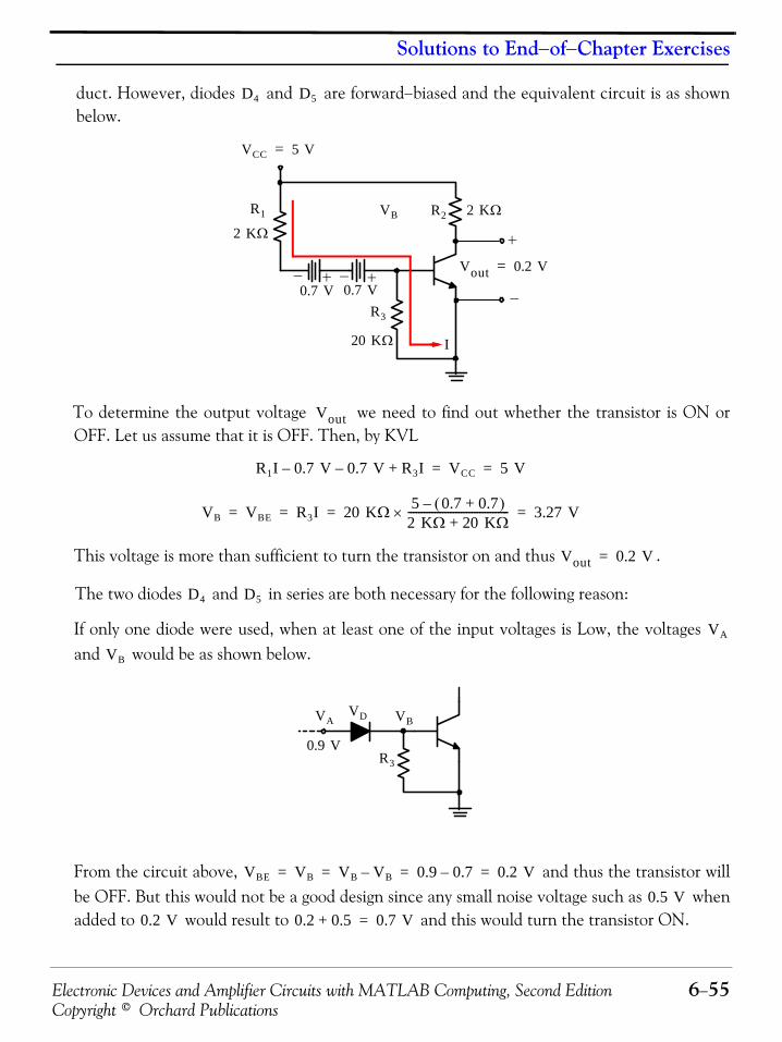
Electronic Devices and Amplifier Circuits with MATLAB Computing, Second Edition 6−55Copyright © Orchard Publications
Solutions to End−of−Chapter Exercises
duct. However, diodes and are forward−biased and the equivalent circuit is as shownbelow.
To determine the output voltage we need to find out whether the transistor is ON orOFF. Let us assume that it is OFF. Then, by KVL
This voltage is more than sufficient to turn the transistor on and thus .
The two diodes and in series are both necessary for the following reason:
If only one diode were used, when at least one of the input voltages is Low, the voltages and would be as shown below.
From the circuit above, and thus the transistor willbe OFF. But this would not be a good design since any small noise voltage such as whenadded to would result to and this would turn the transistor ON.
D4 D5
0.7 V0.7 V
VCC 5 V=
R1 R2
R3
20 KΩ
2 KΩ
2 KΩVB
Vout 0.2 V=
I
Vout
R1I 0.7 V– 0.7 V– R3I+ VCC 5 V= =
VB VBE R3I 20 KΩ 5 0.7 0.7+( )–2 KΩ 20 KΩ+--------------------------------------× 3.27 V= = = =
Vout 0.2 V=
D4 D5
VA
VB
VBVAVD
R30.9 V
VBE VB VB VB– 0.9 0.7– 0.2 V= = = =
0.5 V0.2 V 0.2 0.5+ 0.7 V=

Chapter 6 Integrated Circuits
6−56 Electronic Devices and Amplifier Circuits with MATLAB Computing, Second EditionCopyright © Orchard Publications
The truth table for this 3−input DTL gate is shown below and we see that it behaves like a 3−input NAND gate.
Note: Like the RTL, DTL is no longer used as a logic family. It is one of the earlier familiesemployed years ago with power consumption of about and propagation delay time ofapproximately .
8.With the circuit is as shown below.
By the voltage division expression
and this voltage will certainly keep the transistor at cutoff. Therefore, for , and the inversion operation has been performed.
Inputs Output
0 V 0 V 0 V 5 V0 V 0 V 5 V 5 V0 V 5 V 0 V 5 V0 V 5 V 5 V 5 V5 V 0 V 0 V 5 V5 V 0 V 5 V 5 V5 V 5 V 0 V 5 V5 V 5 V 5 V 0 V
V1 V2 V3 Vout
10 mW30 ns
vin 0 V=
vout 12 V=
VCC 12 V=
100
2.2 KΩ
15 KΩ
KΩ
VBB 12– V=
VB
VB VBE15 KΩ
100 KΩ 15 KΩ+-------------------------------------------- 12 V–( )⋅ 1.57 V–= = =
vin 0 V=
vout 12 V=

Electronic Devices and Amplifier Circuits with MATLAB Computing, Second Edition 6−57Copyright © Orchard Publications
Solutions to End−of−Chapter Exercises
With the circuit is as shown below. First let us assume that toobtain approximate values and verify the assumption that the transistor is indeed in saturation.
Let the minimum base current for saturation be denoted as . Then, where
and thus
The actual base current can be found from the circuit above. We find that
and
Since this value is considerably larger than , we accept the fact that the transistor is insaturation.
Next, we assume that to obtain more exact values. The circuit then is asshown below, and since the transistor is in saturation, there must be
and with these values,
vin 12 V= vout sat( ) 0 V=
vin 12 V=
IC
VCC 12 V=
I1
100
2.2 KΩ
KΩKΩ
VBB 12– V=
IBVB
vout sat( ) 0 V=
15
I2
IB min( ) IB min( ) IC hFE⁄=
IC12 V
2.2 KΩ----------------- 5.45 mA= =
IB min( )IC
hFE------- 5.45 mA
30---------------------- 0.182 mA= = =
I112 V
15 KΩ----------------- 0.80 mA= =
I212 V
100 KΩ-------------------- 0.12 mA= =
IB I1 I2– 0.80 0.12– 0.68 mA= = =
IB min( )
vout sat( ) 0.2 V=
vBE sat( ) 0.7 V=

Chapter 6 Integrated Circuits
6−58 Electronic Devices and Amplifier Circuits with MATLAB Computing, Second EditionCopyright © Orchard Publications
and
We observe that the more exact computations do not differ significantly from those obtainedby assuming that the transistor in saturation is essentially a short circuit. Therefore, when
, and again the inversion operation is performed.
IC12 V 0.2–
2.2 KΩ------------------------ 5.1 mA= =
IB min( )IC
hFE------- 5.1 mA
30------------------- 0.17 mA= = =
I112 V 0.7 V–
15 KΩ-------------------------------- 0.75 mA= =
I20.7 V 12 V–( )–
100 KΩ---------------------------------------- 0.13 mA= =
IB I1 I2– 0.75 0.13– 0.62 mA= = =
vin 12 V= vout sat( ) 0.2 V=

Electronic Devices and Amplifier Circuits with MATLAB Computing, Second Edition 7−1Copyright © Orchard Publications
Chapter 7
Pulse Circuits and Waveform Generators
his chapter is an introduction to several pulsed circuits and waveform generators also knownas relaxation oscillators. These circuits are part of a family of circuits that include differenti-ators, integrators, clipping and clamping circuits, pulse−timing and delay circuits, logic cir-
cuits, and switching circuits. In this chapter we discuss the three types of multivibrators, the 555Timer, and the Schmitt trigger. Sinusoidal oscillators are discussed in Chapter 10.
7.1 Astable (Free−Running) MultivibratorsAn astable or free−running multivibrator, shown in Figure 7.1, is essentially a digital clock which hastwo momentarily stable states which alternate continuously thus producing square pulses as shownin Figure 7.2. We have assumed that all devices in the circuit of Figure 7.1 are identical.
Figure 7.1. Astable multivibrator
Figure 7.2. Output waveforms of the astable multivibrator
Let us now consider Output 1 and assume that the time ON and time OFF are equal andthe period is as shown in Figure 7.3.
T
VCC
RC RCRB RB
Q1 Q2
C COutput 1 Output 2
Output 1
Output 2
T1 T2
T
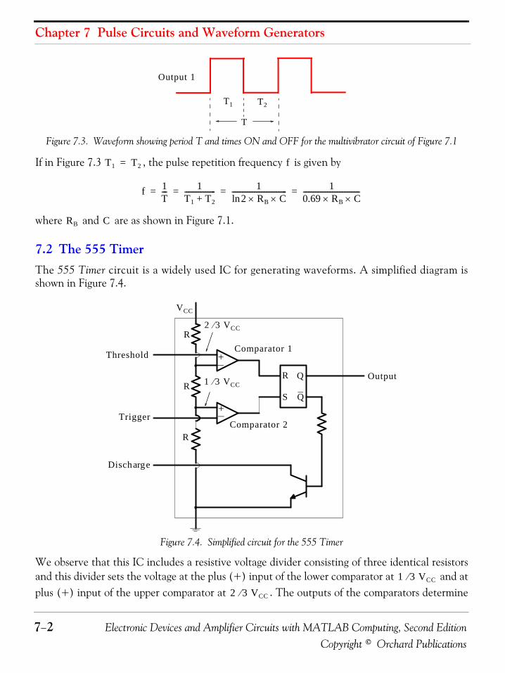
Chapter 7 Pulse Circuits and Waveform Generators
7−2 Electronic Devices and Amplifier Circuits with MATLAB Computing, Second EditionCopyright © Orchard Publications
Figure 7.3. Waveform showing period T and times ON and OFF for the multivibrator circuit of Figure 7.1
If in Figure 7.3 , the pulse repetition frequency is given by
where and are as shown in Figure 7.1.
7.2 The 555 TimerThe 555 Timer circuit is a widely used IC for generating waveforms. A simplified diagram isshown in Figure 7.4.
Figure 7.4. Simplified circuit for the 555 Timer
We observe that this IC includes a resistive voltage divider consisting of three identical resistorsand this divider sets the voltage at the plus (+) input of the lower comparator at and atplus (+) input of the upper comparator at . The outputs of the comparators determine
Output 1
T
T1 T2
T1 T2= f
f 1T--- 1
T1 T2+------------------ 1
2 RB C××ln-------------------------------- 1
0.69 RB C××---------------------------------= = = =
RB C
VCC
R
+
+
Disch earg
Trigger
Threshold
Output
S Q
Q
Comparator 2
Comparator 1R
R
R
2 3⁄ VCC
1 3⁄ VCC
1 3⁄ VCC
2 3⁄ VCC
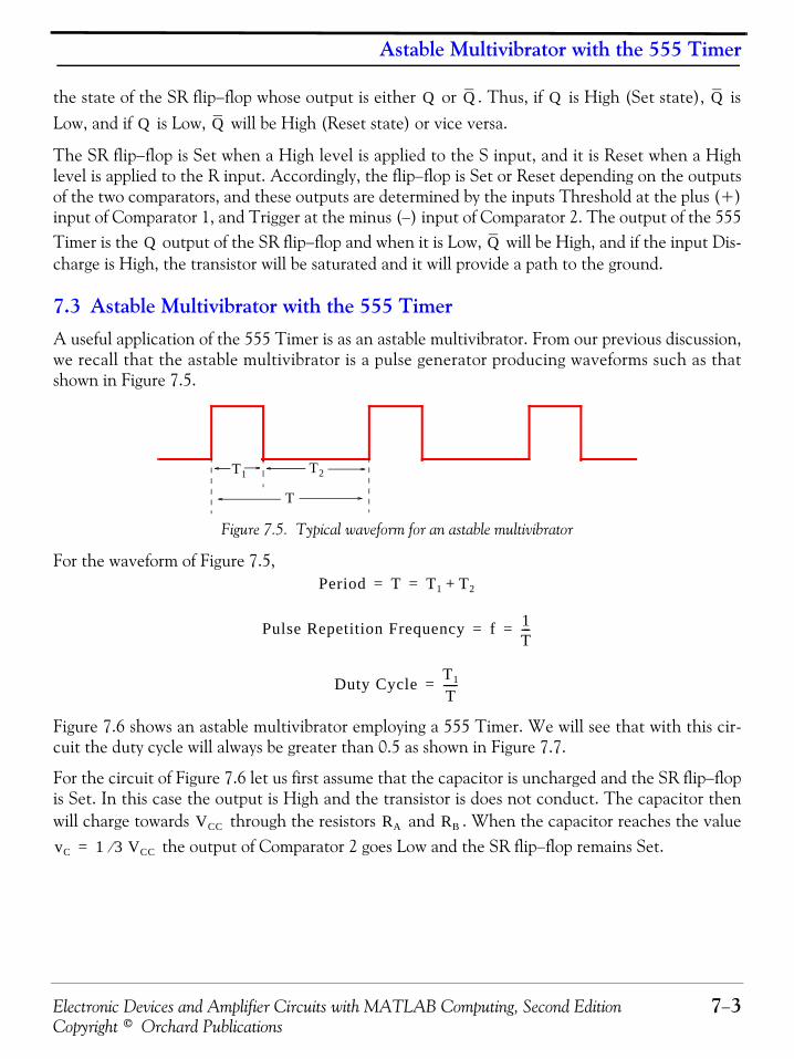
Electronic Devices and Amplifier Circuits with MATLAB Computing, Second Edition 7−3Copyright © Orchard Publications
Astable Multivibrator with the 555 Timer
the state of the SR flip−flop whose output is either or . Thus, if is High (Set state), isLow, and if is Low, will be High (Reset state) or vice versa.
The SR flip−flop is Set when a High level is applied to the S input, and it is Reset when a Highlevel is applied to the R input. Accordingly, the flip−flop is Set or Reset depending on the outputsof the two comparators, and these outputs are determined by the inputs Threshold at the plus (+)input of Comparator 1, and Trigger at the minus (−) input of Comparator 2. The output of the 555Timer is the output of the SR flip−flop and when it is Low, will be High, and if the input Dis-charge is High, the transistor will be saturated and it will provide a path to the ground.
7.3 Astable Multivibrator with the 555 TimerA useful application of the 555 Timer is as an astable multivibrator. From our previous discussion,we recall that the astable multivibrator is a pulse generator producing waveforms such as thatshown in Figure 7.5.
Figure 7.5. Typical waveform for an astable multivibrator
For the waveform of Figure 7.5,
Figure 7.6 shows an astable multivibrator employing a 555 Timer. We will see that with this cir-cuit the duty cycle will always be greater than 0.5 as shown in Figure 7.7.
For the circuit of Figure 7.6 let us first assume that the capacitor is uncharged and the SR flip−flopis Set. In this case the output is High and the transistor is does not conduct. The capacitor thenwill charge towards through the resistors and . When the capacitor reaches the value
the output of Comparator 2 goes Low and the SR flip−flop remains Set.
Q Q Q QQ Q
Q Q
T
T1 T2
Period T T1 T2+= =
Pulse Repetition Frequency f 1T---= =
Duty Cycle T1
T-----=
VCC RA RB
vC 1 3⁄ VCC=

Chapter 7 Pulse Circuits and Waveform Generators
7−4 Electronic Devices and Amplifier Circuits with MATLAB Computing, Second EditionCopyright © Orchard Publications
Figure 7.6. Implementation of an astable multivibrator with a 555 Timer
Figure 7.7. Input and output waveforms for the astable multivibrator of Figure 7.6
When the capacitor reaches the value , the output of Comparator 1 goes High and
resets the SR flip−flop and thus the output goes Low, goes High, the transistor becomes sat-urated, its collector voltage becomes almost zero, and since it appears at the common node ofresistors and , the capacitor begins to discharge through resistor and the collector ofthe transistor. The capacitor voltage decreases exponentially with time constant
RA
RB
C
vC
VCC
R
R
R
2 3⁄ VCC
1 3⁄ VCC
Comparator 1
Comparator 2
OutputR
S Q
Q
+
+
T1 T2
T2T1
vC 2 3⁄ VCC=
vC 1 3⁄ VCC=
Output waveform
vC 2 3⁄ VCC=
Q Q
RA RB RB
vC td RBC=
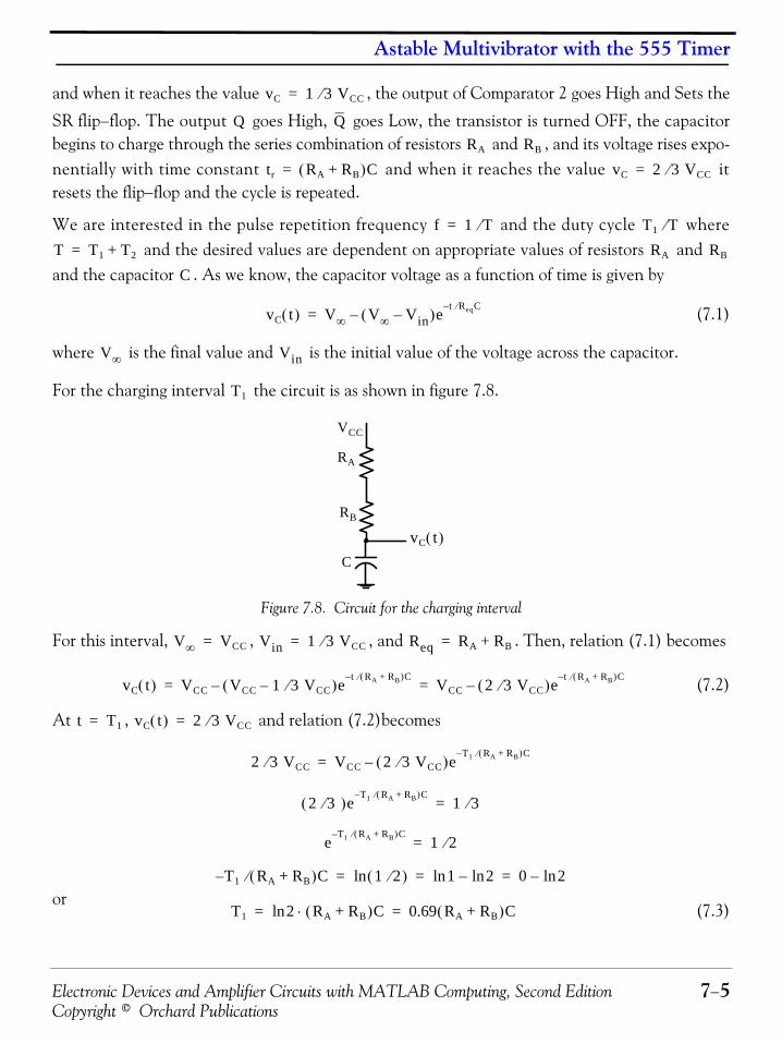
Electronic Devices and Amplifier Circuits with MATLAB Computing, Second Edition 7−5Copyright © Orchard Publications
Astable Multivibrator with the 555 Timer
and when it reaches the value , the output of Comparator 2 goes High and Sets the
SR flip−flop. The output goes High, goes Low, the transistor is turned OFF, the capacitorbegins to charge through the series combination of resistors and , and its voltage rises expo-nentially with time constant and when it reaches the value itresets the flip−flop and the cycle is repeated.
We are interested in the pulse repetition frequency and the duty cycle where and the desired values are dependent on appropriate values of resistors and
and the capacitor . As we know, the capacitor voltage as a function of time is given by
(7.1)
where is the final value and is the initial value of the voltage across the capacitor.
For the charging interval the circuit is as shown in figure 7.8.
Figure 7.8. Circuit for the charging interval
For this interval, , , and . Then, relation (7.1) becomes
(7.2)
At , and relation (7.2)becomes
or(7.3)
vC 1 3⁄ VCC=
Q QRA RB
tr RA RB+( )C= vC 2 3⁄ VCC=
f 1 T⁄= T1 T⁄T T1 T2+= RA RB
C
vC t( ) V∞ V∞ Vin–( )e t ReqC⁄––=
V∞ Vin
T1
vC t( )C
RA
VCC
RB
V∞ VCC= Vin 1 3⁄ VCC= Req RA RB+=
vC t( ) VCC VCC 1 3⁄ VCC–( )e t RA RB+( )C⁄–– VCC 2 3⁄ VCC( )e t RA RB+( )C⁄–
–= =
t T1= vC t( ) 2 3⁄ VCC=
2 3⁄ VCC VCC 2 3⁄ VCC( )eT1 RA RB+( )C⁄–
–=
2 3⁄ ( )e T1 RA RB+( )C⁄– 1 3⁄=
e T1 RA RB+( )C⁄– 1 2⁄=
T1 RA RB+( )C⁄– 1 2⁄( )ln 1 2ln–ln 0 2ln–= = =
T1 2ln RA RB+( )C⋅ 0.69 RA RB+( )C= =
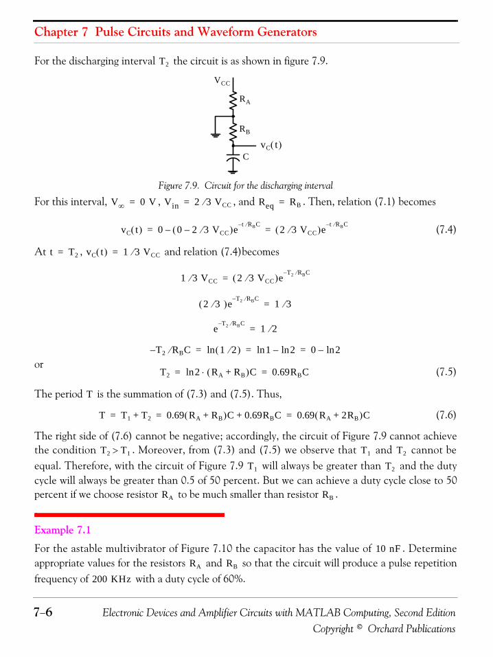
Chapter 7 Pulse Circuits and Waveform Generators
7−6 Electronic Devices and Amplifier Circuits with MATLAB Computing, Second EditionCopyright © Orchard Publications
For the discharging interval the circuit is as shown in figure 7.9.
Figure 7.9. Circuit for the discharging interval
For this interval, , , and . Then, relation (7.1) becomes
(7.4)
At , and relation (7.4)becomes
or(7.5)
The period is the summation of (7.3) and (7.5). Thus,
(7.6)
The right side of (7.6) cannot be negative; accordingly, the circuit of Figure 7.9 cannot achievethe condition . Moreover, from (7.3) and (7.5) we observe that and cannot beequal. Therefore, with the circuit of Figure 7.9 will always be greater than and the dutycycle will always be greater than 0.5 of 50 percent. But we can achieve a duty cycle close to 50percent if we choose resistor to be much smaller than resistor .
Example 7.1
For the astable multivibrator of Figure 7.10 the capacitor has the value of . Determineappropriate values for the resistors and so that the circuit will produce a pulse repetitionfrequency of with a duty cycle of 60%.
T2
RA
RB
CvC t( )
VCC
V∞ 0 V= Vin 2 3⁄ VCC= Req RB=
vC t( ) 0 0 2 3⁄ VCC–( )e t RBC⁄–– 2 3⁄ VCC( )e t RBC⁄–
= =
t T2= vC t( ) 1 3⁄ VCC=
1 3⁄ VCC 2 3⁄ VCC( )eT2 RBC⁄–
=
2 3⁄ ( )e T2 RBC⁄– 1 3⁄=
e T2 RBC⁄– 1 2⁄=
T2 RBC⁄– 1 2⁄( )ln 1 2ln–ln 0 2ln–= = =
T2 2ln RA RB+( )C⋅ 0.69RBC= =
T
T T1 T2+ 0.69 RA RB+( )C 0.69RBC+ 0.69 RA 2RB+( )C= = =
T2 T1> T1 T2
T1 T2
RA RB
10 nFRA RB
200 KHz

Electronic Devices and Amplifier Circuits with MATLAB Computing, Second Edition 7−7Copyright © Orchard Publications
Astable Multivibrator with the 555 Timer
Figure 7.10. Astable multivibrator for Example 7.1
Solution:
The period is a function of the capacitor and resistor values as shown in relation(7.6), that is,
The pulse repetition frequency is and thus
(7.7)
The duty cycle is and from relations (7.3) and (7.6) we obtain
(7.8)
Subtraction of (7.8) from (7.7) yields
RA
RB
C
vC
VCC
R
R
R
2 3⁄ VCC
1 3⁄ VCC
Comparator 1
Comparator 2
OutputR
S Q
Q
+
+
T1 T2
T T1 T2+=
T T1 T2+ 0.69 RA 2RB+( )C= =
f 1 T⁄=
f 105 10.69 RA 2RB+( )C------------------------------------------- 1.443 108×
RA 2RB+---------------------------= = =
RA 2RB+ 1.443 108×105
--------------------------- 14.43 KΩ= =
T1 T⁄
Duty cycle 0.6 T1
T----- 0.69 RA RB+( )C
0.69 RA 2RB+( )C------------------------------------------- RA RB+
RA 2RB+----------------------- RA RB+
14.43 KΩ-------------------------= = = = =
RA RB+ 0.6 14.43× 8.66 KΩ= =
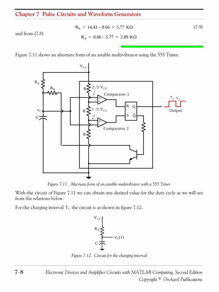
Chapter 7 Pulse Circuits and Waveform Generators
7−8 Electronic Devices and Amplifier Circuits with MATLAB Computing, Second EditionCopyright © Orchard Publications
(7.9)and from (7.8)
Figure 7.11 shows an alternate form of an astable multivibrator using the 555 Timer.
Figure 7.11. Alternate form of an astable multivibrator with a 555 Timer
With the circuit of Figure 7.11 we can obtain any desired value for the duty cycle as we will seefrom the relations below.
For the charging interval the circuit is as shown in figure 7.12.
Figure 7.12. Circuit for the charging interval
RB 14.43 8.66– 5.77 KΩ= =
RA 8.66 5.77– 2.89 KΩ= =
VCC
RA
RB
vC
C
R
R
R
2 3⁄ VCC
1 3⁄ VCC
Comparator 1
Comparator 2
R
S Q
Q
+
+
Output
T1 T2
T1
VCC
RA
CvC t( )

Electronic Devices and Amplifier Circuits with MATLAB Computing, Second Edition 7−9Copyright © Orchard Publications
Astable Multivibrator with the 555 Timer
For this interval, , , and . Then, relation (7.1) becomes
(7.10)
At , and relation (7.10) becomes
(7.11)
For the discharging interval the circuit is as shown in figure 7.13.
Figure 7.13. Circuit for the discharging interval
For this interval, , , and . Then, rela-tion (7.1) becomes
(7.12)
At , and relation (7.12)becomes
(7.13)
V∞ VCC= Vin 1 3⁄ VCC= Req RA=
vC t( ) VCC VCC 1 3⁄ VCC–( )et RAC⁄–
– VCC 2 3⁄ VCC( )et RAC⁄–
–= =
t T1= vC t( ) 2 3⁄ VCC=
2 3⁄ VCC VCC 2 3⁄ VCC( )e t RAC⁄––=
2 3⁄ ( )e t RAC⁄– 1 3⁄=
e t RAC⁄– 1 2⁄=
T1 RAC⁄– 1 2⁄( )ln 1 2ln–ln 0 2ln–= = =
T1 2ln RAC⋅ 0.69RAC= =
T2
VCC
RA
C
vC t( )
RB
V∞ RB RA RB+( )⁄( )VCC= Vin 2 3⁄ VCC= Req RA RB||=
vC t( )RB
RA RB+--------------------⎝ ⎠
⎛ ⎞VCCRB
RA RB+--------------------⎝ ⎠
⎛ ⎞VCC 2 3⁄ VCC– e t RA RB||( )C⁄––=
t T2= vC t( ) 1 3⁄ VCC=
1 3⁄ VCCRB
RA RB+--------------------⎝ ⎠
⎛ ⎞VCCRB
RA RB+--------------------⎝ ⎠
⎛ ⎞VCC 2 3⁄ VCC– e T2 RA RB||( )C⁄––=
e T2 RA RB||( )C⁄– 1 3⁄ RB RA RB+( )⁄–[ ]VCC
2 3⁄ RB RA RB+( )⁄–[ ]VCC----------------------------------------------------------------------
RA 2RB–2RA RB–-----------------------⎝ ⎠
⎛ ⎞= =
e T2 RBC⁄– 1 2⁄=

Chapter 7 Pulse Circuits and Waveform Generators
7−10 Electronic Devices and Amplifier Circuits with MATLAB Computing, Second EditionCopyright © Orchard Publications
or(7.14)
However, there is one restriction as we can see from relation (7.13), that is, the term must be less than . Therefore, the period is the summation of (7.11) and
(7.14) from which we obtain the relation
(7.15)
subject to the condition that , and this condition can be simplified asshown below.
(7.16)
Example 7.2
Using the astable multivibrator of Figure 7.11 find an appropriate ratio for resistors and sothat the output will be a square waveform, i.e., a waveform with duty cycle at .
Solution:
To achieve a duty cycle at , we must make and this condition will be satisfied if weequate relations (7.11) and (7.14) subject to the constraint of (7.16). Then,
T2 RA RB||( )C⁄–RA 2RB–2RA RB–-----------------------⎝ ⎠
⎛ ⎞ln RA 2RB–( ) 2RA RB–( )ln–ln= =
T2 RA RB||( )C⁄ 2RA RB–( )ln RA 2RB–( )ln–2RA RB–RA 2RB–-----------------------⎝ ⎠
⎛ ⎞ln= =
T2RA RB⋅RA RB+--------------------C
2RA RB–RA 2RB–-----------------------⎝ ⎠
⎛ ⎞ln⋅=
RB RA RB+( )⁄ 1 3⁄ T
T T1 T2+ 0.69RACRA RB⋅RA RB+--------------------C
2RA RB–RA 2RB–-----------------------⎝ ⎠
⎛ ⎞ln⋅+= =
T 0.69RARA RB⋅RA RB+--------------------+ C
2RA RB–RA 2RB–-----------------------⎝ ⎠
⎛ ⎞ln⋅ ⋅=
RB RA RB+( )⁄ 1 3⁄<
RB
RA RB+-------------------- 1 3⁄<
3RB RA RB+<
2RB RA<
RB RA 2⁄<
RA RB
50 %
50 % T1 T2=
2RAClnRA RB⋅RA RB+--------------------C
2RA RB–RA 2RB–-----------------------⎝ ⎠
⎛ ⎞ln⋅=
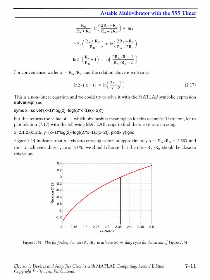
Electronic Devices and Amplifier Circuits with MATLAB Computing, Second Edition 7−11Copyright © Orchard Publications
Astable Multivibrator with the 555 Timer
For convenience, we let and the relation above is written as
(7.17)
This is a non−linear equation and we could try to solve it with the MATLAB symbolic expressionsolve(‘eqn’) as
syms x; solve('(x+1)*log(2)=log((2*x−1)/(x−2))')
but this returns the value of which obviously is meaningless for this example. Therefore, let usplot relation (7.17) with the following MATLAB script to find the x−axis zero crossing.
x=2.1:0.01:2.5; y=(x+1)*log(2)−log((2.*x−1)./(x−2)); plot(x,y);grid
Figure 7.14 indicates that x−axis zero crossing occurs at approximately andthus to achieve a duty cycle at , we should choose that the ratio should be close tothis value.
Figure 7.14. Plot for finding the ratio to achieve duty cycle for the circuit of Figure 7.14
RB
RA RB+-------------------- 2RA RB–
RA 2RB–-----------------------⎝ ⎠
⎛ ⎞ln⋅ 2ln=
2lnRA RB+
RB--------------------⎝ ⎠
⎛ ⎞⋅2RA RB–RA 2RB–-----------------------⎝ ⎠
⎛ ⎞ln=
2ln RA
RB------ 1+⎝ ⎠
⎛ ⎞⋅2RA RB⁄ 1–RA RB⁄ 2–
------------------------------⎝ ⎠⎛ ⎞ln=
x RA RB⁄=
2ln x 1+( )⋅ 2x 1–x 2–
---------------⎝ ⎠⎛ ⎞ln=
1–
x RA RB⁄ 2.363= =
50 % RA RB⁄
2.1 2.15 2.2 2.25 2.3 2.35 2.4 2.45 2.5
-1.2
-1
-0.8
-0.6
-0.4
-0.2
0
0.2
0.4
x=RA/RB
Rel
atio
n (7
.17)
RA RB⁄ 50 %
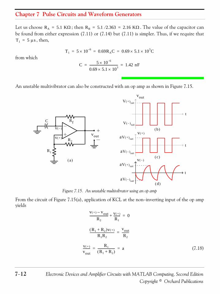
Chapter 7 Pulse Circuits and Waveform Generators
7−12 Electronic Devices and Amplifier Circuits with MATLAB Computing, Second EditionCopyright © Orchard Publications
Let us choose ; then . The value of the capacitor canbe found from either expression (7.11) or (7.14) but (7.11) is simpler. Thus, if we require that
, then,
from which
An unstable multivibrator can also be constructed with an op amp as shown in Figure 7.15.
Figure 7.15. An unstable multivibrator using an op amp
From the circuit of Figure 7.15(a), application of KCL at the non−inverting input of the op ampyields
(7.18)
RA 5.1 KΩ= RB 5.1 2.363⁄ 2.16 KΩ= =
T1 5 μs=
T1 5 10 6–× 0.69RAC 0.69 5.1× 10³× C= = =
C 5 10 6–×0.69 5.1× 10³×-------------------------------------- 1.42 nF= =
Rf
R2
R1
vout
C V −( )sat
vout
t
t
t
V +( )sat
v +( )v +( )
v −( )
v −( )aV +( )sat
aV −( )sat
aV −( )sat
aV +( )sat
a( )
d( )
c( )
b( )
v +( ) vout–
R2------------------------- v +( )
R1---------+ 0=
R1 R2+( )v +( )
R1R2---------------------------------
voutR2
----------=
v +( )
vout---------- R1
R1 R2+( )----------------------- a= =
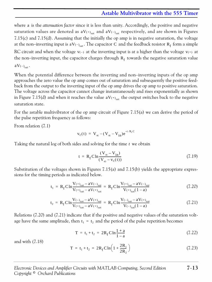
Electronic Devices and Amplifier Circuits with MATLAB Computing, Second Edition 7−13Copyright © Orchard Publications
Astable Multivibrator with the 555 Timer
where is the attenuation factor since it is less than unity. Accordingly, the positive and negativesaturation values are denoted as and respectively, and are shown in Figures7.15(c) and 7.15(d). Assuming that the initially the op amp is in negative saturation, the voltageat the non−inverting input is . The capacitor and the feedback resistor form a simple
RC circuit and when the voltage at the inverting input is at a higher than the voltage atthe non−inverting input, the capacitor charges through towards the negative saturation value
.
When the potential difference between the inverting and non−inverting inputs of the op ampapproaches the zero value the op amp comes out of saturation and subsequently the positive feed-back from the output to the inverting input of the op amp drives the op amp to positive saturation.The voltage across the capacitor cannot change instantaneously and rises exponentially as shownin Figure 7.15(d) and when it reaches the value the output switches back to the negativesaturation state.
For the astable multivibrator of the op amp circuit of Figure 7.15(a) we can derive the period ofthe pulse repetition frequency as follows:
From relation (7.1)
Taking the natural log of both sides and solving for the time we obtain
(7.19)
Substitution of the voltages shown in Figures 7.15(a) and 7.15(b) yields the appropriate expres-sions for the timing periods as indicated below.
(7.20)
(7.21)
Relations (7.20) and (7.21) indicate that if the positive and negative values of the saturation volt-age have the same amplitude, then and the period of the pulse repetition becomes
(7.22)
and with (7.18) (7.23)
aaV +( )sat aV −( )sat
aV −( )sat C Rf
v −( ) v +( )
Rf
aV −( )sat
aV +( )sat
vC t( ) V∞ V∞ Vin–( )e t Rf C⁄––=
t
t Rf CV∞ Vin–( )
V∞ vC t( )–( )-------------------------------ln=
t1 Rf CV +( )sat aV −( )sat–
V +( )sat aV +( )sat–----------------------------------------ln Rf C
V +( )sat aV −( )sat–
V +( )sat 1 a–( )----------------------------------------ln= =
t2 Rf CV −( )sat aV +( )sat–
V +( )sat aV +( )sat–----------------------------------------ln Rf C
V −( )sat aV +( )sat–
V −( )sat 1 a–( )----------------------------------------ln= =
t1 t2=
T t1 t2+ 2Rf C 1 a+1 a–------------ln= =
T t1 t2+ 2Rf C 1 2R1
2R2---------+⎝ ⎠
⎛ ⎞ln= =

Chapter 7 Pulse Circuits and Waveform Generators
7−14 Electronic Devices and Amplifier Circuits with MATLAB Computing, Second EditionCopyright © Orchard Publications
Example 7.3
For the astable multivibrator circuit of Figure 7.16 compute the timing periods given that, , , , , and .
Figure 7.16. Unstable multivibrator circuit for Example 7.3Solution:
From (7.18) the attenuation factor is
and with (7.20) and (7.21)
7.4 Monostable (One−Shot) MultivibratorsA monostable or one−shot multivibrator is an electronic circuit with two output states in which onlyone state is stable. This circuit stays in its normal state (usually a logical 0) until a signal isapplied to its input. When triggered by an input signal, the output reverses states, that is, changesfrom 0 to 1 for a short period of time, depending upon the circuit parameters which are discussedbelow, and then returns to its normal state.
C 0.1 μF= Rf 50 KΩ= R1 10 KΩ= R2 50 KΩ= V +( )sat 10 V= V −( )sat 5– V=
Rf
R2
R1
vout
C
V −( )sat
vout
t
V +( )sat
v +( )
v −( )
a( ) b( )
a R1
R1 R2+( )----------------------- 10
10 500+--------------------- 1
6---= = =
t1 Rf CV +( )sat aV −( )sat–
V +( )sat 1 a–( )----------------------------------------ln 50 104× 0.1 10 6– 10 1 6⁄( ) 5–( )–
10 1 1 6⁄–( )×--------------------------------------⎝ ⎠
⎛ ⎞ln××= =
5 10 2– 65 6⁄50 6⁄-------------⎝ ⎠
⎛ ⎞ln× 1.31 ms==
t2 Rf CV −( )sat aV +( )sat–
V −( )sat 1 a–( )----------------------------------------ln 50 104× 0.1 10 6– 5– 1 6⁄( ) 10( )–
5– 1 1 6⁄–( )×---------------------------------------⎝ ⎠
⎛ ⎞ln××==
5 10 2– 40– 6⁄25– 6⁄
----------------⎝ ⎠⎛ ⎞ln× 2.35 ms==

Electronic Devices and Amplifier Circuits with MATLAB Computing, Second Edition 7−15Copyright © Orchard Publications
Monostable (One−Shot) Multivibrators
Figure 7.17 shows a block diagram of a typical monostable and its input and output waveforms.
Figure 7.17. Block diagram and typical input and output waveforms for a monostable multivibrator
We observe that a positive going pulse at the input signal (transition from A to B) which is oftenreferred to as the leading edge of the pulse (the transition from C to D is referred to as the trailingedge of the pulse) makes the 0 output to change state momentarily from state 0 to state 1 for a timeperiod designated as which is determined by an external resistor and an external capacitor
as shown in Figure 7.18. Device SN74121 is a typical monostable multivibrator circuit and it isshown in Figure 7.18.
Figure 7.18. The 74121 monostable multivibrator
As shown in Figure 7.18, the 74121 has three trigger inputs: , , and . Depending on thedesired circuit operation, any or all of these three pins may be connected to the input trigger sig-nal. In Figure 7.5 and are both active low and the input is active high. Under those con-ditions, the monostable multivibrator will produce the output pulse shown.
As stated above, time period that the output will stay High is determined by an external resistor and an external capacitor . Typically, the capacitor value is greater than and the
resistor value is greater than and the pulse width period at the output is determinedfrom the relation
For instance, if and , the pulse width will be . With the74121 device, the output pulse width can be varied from to . Also the 74121 is retrigga-ble meaning that the input may be a train of periodic pulses.
Monostable
MultivibratorInput
Q Output
Q Output
DA
CBInput
Q Output T
T RX
CX
B
VCC
4A1 A2
3 7
10 9 14
CX RX
5 6Q
Input Output
74121
A1 A2 B
A1 A2 B
RX CX 1 μF10 KΩ T
T 0.33 RX CX××=
RX 20 KΩ= CX 5 μF= T 100 ms=
40 ns 28 s

Chapter 7 Pulse Circuits and Waveform Generators
7−16 Electronic Devices and Amplifier Circuits with MATLAB Computing, Second EditionCopyright © Orchard Publications
The monostable multivibrator is used primarily in pulse shaping applications. It can be used towiden a narrow pulse as shown in Figure 7.18, and to block unwanted input pulses as shown inFigure 7.19.
Figure 7.19. The use of a monostable multivibrator to block unwanted input pulses
A monostable multivibrator can also be constructed with an op amp as shown in Figure 7.20.
Figure 7.20. A monostable multivibrator using an op amp
In the circuit of Figure 7.20, while the input pulse is zero, i.e., , the op amp remains in
positive saturation, that is, , and this is the stable state of the circuit, hence the
name monostable. At this state, diode is forward biased and the voltage across the capacitor is the same as that of diode , about and thus the voltage across the inverting input of
the op amp is .
By the voltage division expression, the voltage at the non−inverting input of the op amp is
(7.24)
Usually, resistors and are chosen such that and thus . Accordingly,the output of the op amp is held at positive saturation.
Next, let us assume that a negative going pulse whose amplitude exceeds the voltage . Thisvoltage at the non−inverting of the op amp will go momentarily negative and will drive the out-put of the op amp into negative saturation . So, with the output at negative saturation, thevoltage at the non−inverting input will also become negative. But this condition is only tem-
Input
Output
Rf
R2
R1
voutC2
vinR3
D2
C1D1
v -( )v +( )
vin 0=
vout V +( )sat=
D1
C1 D1 0.7 Vv −( ) 0.7 V=
v +( )R2
R1 R2+------------------V +( )sat=
R1 R2 R2 R1⁄ 10= v +( ) v −( )»
v +( )
V −( )sat
v +( )

Electronic Devices and Amplifier Circuits with MATLAB Computing, Second Edition 7−17Copyright © Orchard Publications
Monostable (One−Shot) Multivibrators
porary because diode is now reverse−biased and allows capacitor to charge negatively, andwhen becomes slightly more negative , and the output of the op amp is once again driveninto positive saturation.
We see then that the output of the op amp remains at negative saturation only longenough for capacitor to charge to approximately the value of , and the time is deter-mined by the time constant of capacitor and feedback resistor , and also by the ratio .The expression for the timing period can be derived from relations (7.18) or (7.19) which for themonostable multivibrator is appropriately expressed as
(7.25)
where is the attenuation factor defined as before as
Alternately, we may express (7.25) as
(7.26)
and if we choose , relation (7.26) simplifies to the approximate expression
(7.27)
As with astable multivibrators, we can form a monostable multivibrator using a 555 timer circuitas shown in Figure 7.21. As shown in Figure 7.21, in the stable state the SR flip−flop will be in theReset state keeping the transistor in saturation and thus the capacitor voltage will be close to zerovolts. The voltage at the input terminal is sufficiently high to keep the output of Comparator 2Low. The output will also be Low.
Now, if a negative going pulse is applied at the input, the output of Comparator 2 will go High, theflip−flop will be Set and its output will go High and output will go Low and the transistor willbe at cutoff. At this time, the capacitor will begin charging through resistor and will rise expo-nentially towards the supply voltage . Once the capacitor voltage exceeds the threshold volt-age of Comparator 1, the output of this comparator will go High, the flip−flop will be Reset, thetransistor will go in saturation, and the capacitor will discharge. Thus, the multivibrator will bereturned to it stable state at zero volts level.
D1 C1
v −( ) v +( )
V −( )sat
C1 v +( ) tC1 Rf R1 R2⁄
t Rf C1V −( )sat 0–( )
V −( )sat aV −( )sat–( )---------------------------------------------ln Rf C1
11 a–-----------ln= =
a
a R1
R1 R2+( )-----------------------=
t Rf C1 1 R1
R2------+⎝ ⎠
⎛ ⎞ln=
R2 R1⁄ 10=
t 0.1Rf C1≈
Q
Q QR1
VCC
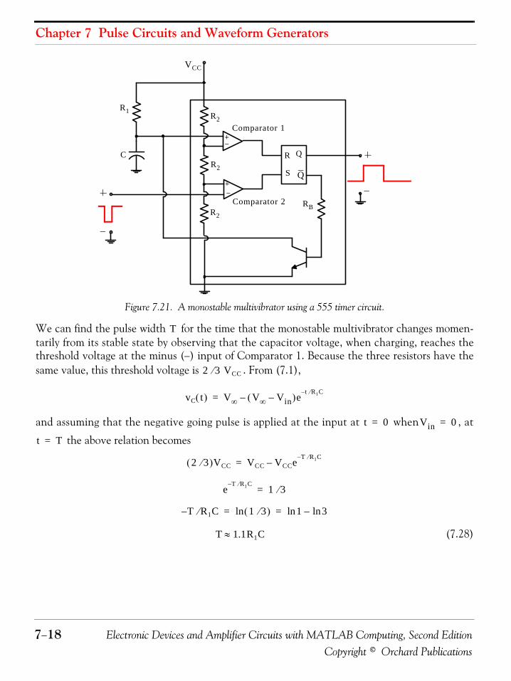
Chapter 7 Pulse Circuits and Waveform Generators
7−18 Electronic Devices and Amplifier Circuits with MATLAB Computing, Second EditionCopyright © Orchard Publications
Figure 7.21. A monostable multivibrator using a 555 timer circuit.
We can find the pulse width for the time that the monostable multivibrator changes momen-tarily from its stable state by observing that the capacitor voltage, when charging, reaches thethreshold voltage at the minus (−) input of Comparator 1. Because the three resistors have thesame value, this threshold voltage is . From (7.1),
and assuming that the negative going pulse is applied at the input at when , at
the above relation becomes
(7.28)
R1
VCC
R
Comparator 1
R2
R2
R2
RB
C
S
Q
Q
Comparator 2
T
2 3 VCC⁄
vC t( ) V∞ V∞ Vin–( )e t R1C⁄––=
t 0= Vin 0=
t T=
2 3⁄( )VCC VCC VCCe T R1C⁄––=
eT R1C⁄– 1 3⁄=
T R1C⁄– 1 3⁄( )ln 1 3ln–ln= =
T 1.1R1C≈

Electronic Devices and Amplifier Circuits with MATLAB Computing, Second Edition 7−19Copyright © Orchard Publications
Bistable Multivibrators (Flip−Flops)
7.5 Bistable Multivibrators (Flip−Flops)
Bistable multivibrators, or more commonly referred to as flip−flops,* are electronic circuits with twostable outputs one of which is the complement of the other. The outputs will change only whendirected by an input command. In this section we will introduce the fixed−bias flip−flop, the self−biased flip−flop, and the Schmitt trigger circuit.
7.5.1 The Fixed−Bias Flip−Flop
The fixed−bias circuit shown in Figure 7.22 is one of the earlier types. For this circuit it is assumedthat the value of the collector resistance is chosen such that the collector current does not exceed the maximum permissible current. It is also assumed that the values of resistors
and , and the bias voltage are selected so that in one state the base current is adequateto drive one transistor into saturation and in the second state the base−emitter junction must bebelow cutoff. The cutoff and saturation characteristics are specified by the manufacturer.
Figure 7.22. Fixed−bias flip−flop circuit
We will illustrate the operation of the circuit of Figure 7.22† with the following example. The trig-gering signal which is used to induce a transition from one state to another will be discussed laterin this section.
Example 7.4
Compute the stable−state currents and voltages for the flip−flop circuit of Figure 7.23. Assumethat the transistors have a minimum value of 50.
* The logic diagrams and characteristic tables for the Set−Reset, Data, J−K, and Toggle flip−flops are described inDigital Circuit Analysis and Design with Simulink Modeling and Introduction to CPLDs and FPGAs, ISBN978−1−934404−05−8.
† This circuit is also known as Ecless−Jordan configuration
RC IC VCC RC⁄≈
R1 R2 VBB
+VCC
V– BB
VC1 VC2
RC RCR1 R1
T1
R2 R2
T2
hFE

Chapter 7 Pulse Circuits and Waveform Generators
7−20 Electronic Devices and Amplifier Circuits with MATLAB Computing, Second EditionCopyright © Orchard Publications
Figure 7.23. Fixed−bias flip−flop circuit for Example 7.4.Solution:This circuit consists of two cross−coupled inverter circuits such as that of Exercise 8 in Chapter6. The analysis is facilitated by breaking the given circuit into two parts, the first part indicatingthe connections between the base of transistor and the collector of transistor as shown inFigure 7.24(a), and the second part indicating the connection between the collector of andthe base of as shown in Figure 7.24(b).
Figure 7.24. Circuits for the computation of the stable states for Example 7.4
Let us first assume that transistor is OFF and transistor is ON. Since the saturation volt-ages are small (about ), we will initially neglect them and we let and
as shown in Figures 7.20(a) and 7.20(b) respectively.By the voltage division expression
and this voltage will certainly keep transistor at cutoff. To verify that with transistor
12 V–
+12 V
2.2 KΩ15 KΩ
2.2 KΩ15 KΩ
VC2VC1
KΩ100 100
KΩ
T1 T2
T1 T2
T1
T2
+12 V +12 V
12 V– 12 V–
T1 T2T1 T2
2.2 KΩ
15 KΩ 15 KΩ
2.2 KΩ
100KΩ KΩ
100
VC2 0 V≈ VC1
OFF ON
ON OFF
VB2 0 V≈VB1IC2
I1I2
IB2
I4
I3
a( ) b( )
T1 T2
0.2 V VC2 sat( ) 0 V≈
VB2 sat( ) 0 V≈
VB115 KΩ
100 KΩ 15 KΩ+-------------------------------------------- 12 V–( )⋅ 1.57 V–= =
T1 T1

Electronic Devices and Amplifier Circuits with MATLAB Computing, Second Edition 7−21Copyright © Orchard Publications
Bistable Multivibrators (Flip−Flops)
beyond cutoff transistor is in saturation, we calculate by first finding and as follows:
Also,
Then,
We observe that the value of is much less than the value of and in a practical flip−flop designthis may not be the case.
Usually, the minimum base current is read from the collector characteristics curve for a partic-ular transistor and since no curves were given, we will use the given minimum value of .for theminimum value of for saturation. Thus,
Let us now compute the value of from Figure 7.24(b). We find that
and
Then,
Since , that is, the value of exceeds the minimum basecurrent value of required for saturation, we have shown that transistor is deeply intosaturation.
Finally, the collector voltage if found from Figure 7.20(b) as
and this value is close to the collector supply voltage of 12 volts.
With the assumption that the saturation are zero volts, the voltages and currents for a stable statefor the flip−flop of this example are summarized in Table 7.1.
The second stable state is the one in which transistor is ON and transistor is OFF. Theanalysis is the same as above where the voltages and currents are interchanged between transistors
and , and .
T2 IC2 I1 I2
I112 V
2.2 KΩ----------------- 5.45 mA= =
I20 12–( )–
15 KΩ 100 KΩ+-------------------------------------------- 0.10 mA= =
IC2 I1 I2– 5.45 0.10– 5.35 mA= = =
I2 I1
IB2
hFE
IB2
IB min( )IC2
hFE------- 5.35 mA
50---------------------- 0.11 mA= = =
IB2
I312
2.2 KΩ 15 KΩ+------------------------------------------ 0.70 mA= =
I412
100 KΩ-------------------- 0.12 mA= =
IB2 I3 I4– 0.70 0.12– 0.58 mA= = =
IB2 0.58 mA=( ) IB min( ) 0.11 mA=( )> IB2
IB min( ) T2
VC1
VC1 12 2.2 103× I3×– 12 2.2 103× 0.70 10 3–××– 10.5 V= = =
T1 T2
T1 T2 VC2 10.5 V=
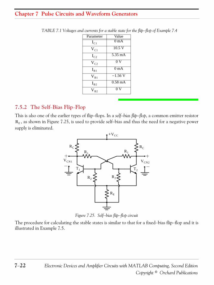
Chapter 7 Pulse Circuits and Waveform Generators
7−22 Electronic Devices and Amplifier Circuits with MATLAB Computing, Second EditionCopyright © Orchard Publications
7.5.2 The Self−Bias Flip−FlopThis is also one of the earlier types of flip−flops. In a self−bias flip−flop, a common emitter resistor
, as shown in Figure 7.25, is used to provide self−bias and thus the need for a negative powersupply is eliminated.
Figure 7.25. Self−bias flip−flop circuit
The procedure for calculating the stable states is similar to that for a fixed−bias flip−flop and it isillustrated in Example 7.5.
TABLE 7.1 Voltages and currents for a stable state for the flip−flop of Example 7.4Parameter Value
0 mA
10.5 V
5.35 mA
0 V
0 mA
−1.56 V
0.58 mA
0 V
IC1
VC1
IC2
VC2
IB1
VB1
IB2
VB2
RE
+VCC
RC RCR1 R1
VCN1 VCN2
T1 T2
R2 R2
RE

Electronic Devices and Amplifier Circuits with MATLAB Computing, Second Edition 7−23Copyright © Orchard Publications
Bistable Multivibrators (Flip−Flops)
Example 7.5
Compute the stable−state currents and voltages for the flip−flop circuit in Figure 7.26 which usesP−N−P identical transistors. Find the minimum value of which will keep the ON transistor insaturation.
Figure 7.26. Self−bias flip−flop circuit for Example 7.5Solution:This circuit consists of two cross−coupled inverter circuits such as that of Exercise 8 in Chapter 6.The analysis is facilitated by breaking the given circuit into two parts, the first part indicating theconnections between the base of transistor and the collector of transistor as shown in Fig-ure 7.27, and the second part indicating the connection between the collector of and the baseof as shown in Figure 7.28.
Let us first assume that transistor is OFF and transistor is ON. We must first compute thevoltage shown in Figure 7.27.
Figure 7.27. The circuit of Example 7.5 showing the connections between the base of and collector of
hFE
VCC– 12 V–
RC
4 KΩ R1
30 KΩ
R1
30 KΩ
RC
4 KΩ
VCN1
T1
R210 KΩ
R2
10 KΩ
RE500ΩVEN1
T2
VEN2
VCN2
T1 T2
T1
T2
T1 T2
VEN1
VCC– 12 V–RC 4 KΩ
R1
30 KΩ
T2
RE
0.5 KΩR2 10 KΩ
T1
OFFON
VBE1
VEN1
VBN1
VCE2
VEN2
VCN2IB2
IB2 IC2+
N
IC2
T1 T2
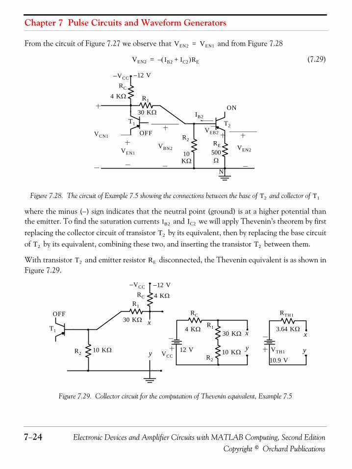
Chapter 7 Pulse Circuits and Waveform Generators
7−24 Electronic Devices and Amplifier Circuits with MATLAB Computing, Second EditionCopyright © Orchard Publications
From the circuit of Figure 7.27 we observe that and from Figure 7.28
(7.29)
Figure 7.28. The circuit of Example 7.5 showing the connections between the base of and collector of
where the minus (−) sign indicates that the neutral point (ground) is at a higher potential thanthe emitter. To find the saturation currents and we will apply Thevenin’s theorem by firstreplacing the collector circuit of transistor by its equivalent, then by replacing the base circuitof by its equivalent, combining these two, and inserting the transistor between them.
With transistor and emitter resistor disconnected, the Thevenin equivalent is as shown inFigure 7.29.
Figure 7.29. Collector circuit for the computation of Thevenin equivalent, Example 7.5
VEN2 VEN1=
VEN2 IB2 IC2+( )RE–=
12 V–
T2
VCN1
4 KΩ
30 KΩ
KΩ Ω500
T1
VCC–RC
R1
R2 REVEN1
VEN210
VBN2
VEB2
ON
N
OFF
IB2
T2 T1
IB2 IC2
T2
T2 T2
T2 RE
VCC12 V
RC
4 KΩR1
30 KΩ
R210 KΩ
T1
OFF
y VTH1
RTH1
10.9 V
3.64 KΩx
y y
x x
RC 4 KΩR1
30 KΩ
R2 10 KΩ
VCC– 12– V
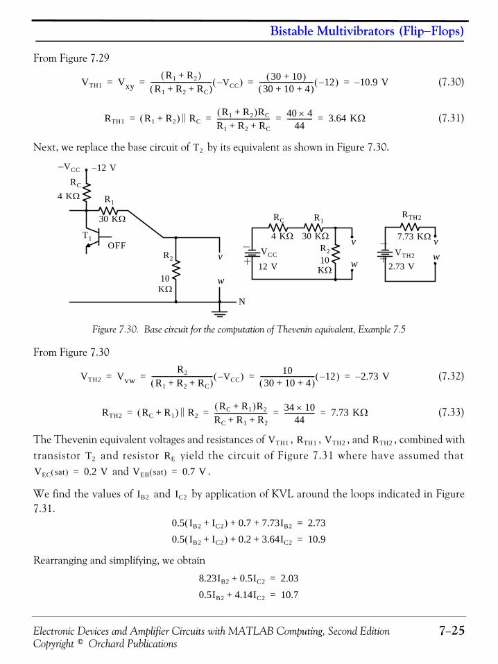
Electronic Devices and Amplifier Circuits with MATLAB Computing, Second Edition 7−25Copyright © Orchard Publications
Bistable Multivibrators (Flip−Flops)
From Figure 7.29
(7.30)
(7.31)
Next, we replace the base circuit of by its equivalent as shown in Figure 7.30.
Figure 7.30. Base circuit for the computation of Thevenin equivalent, Example 7.5
From Figure 7.30
(7.32)
(7.33)
The Thevenin equivalent voltages and resistances of , , , and , combined withtransistor and resistor yield the circuit of Figure 7.31 where have assumed that
and .
We find the values of and by application of KVL around the loops indicated in Figure7.31.
Rearranging and simplifying, we obtain
VTH1 VxyR1 R2+( )
R1 R2 RC+ +( )------------------------------------ VCC–( ) 30 10+( )
30 10 4+ +( )-------------------------------- 12–( ) 10.9 V–= = = =
RTH1 R1 R2+( ) RC|| R1 R2+( )RC
R1 R2 RC+ +------------------------------- 40 4×
44--------------- 3.64 KΩ= = = =
T2
12 V–
4 KΩ
30 KΩ
KΩ
T1
VCC–
RC
R1
R2
10
N
OFF
12 V
RC R1
4 KΩ 30 KΩR210
KΩ
VCCvv v
ww
w2.73 V
VTH2
RTH2
7.73 KΩ
VTH2 VvwR2
R1 R2 RC+ +( )------------------------------------ VCC–( ) 10
30 10 4+ +( )-------------------------------- 12–( ) 2.73 V–= = = =
RTH2 RC R1+( ) R2|| RC R1+( )R2
RC R1 R2+ +------------------------------- 34 10×
44------------------ 7.73 KΩ= = = =
VTH1 RTH1 VTH2 RTH2
T2 RE
VEC sat( ) 0.2 V= VEB sat( ) 0.7 V=
IB2 IC2
0.5 IB2 IC2+( ) 0.7 7.73IB2+ + 2.73=
0.5 IB2 IC2+( ) 0.2 3.64IC2+ + 10.9=
8.23IB2 0.5IC2+ 2.03=
0.5IB2 4.14IC2+ 10.7=

Chapter 7 Pulse Circuits and Waveform Generators
7−26 Electronic Devices and Amplifier Circuits with MATLAB Computing, Second EditionCopyright © Orchard Publications
Figure 7.31. The composite Thevenin equivalent circuit of Example 7.5 when transistor is in saturation
Using MATLAB with the matrix left division operator, we obtain write and execute the follow-ing script which produces the values of the currents and .
A=[8.23 0.5; 0.5 4.14]; B=[2.03 10.7]'; x=A\B;...fprintf(' \n'); fprintf('IB2=%2.3f mA \t',x(1)); fprintf('IC2=%2.3f mA \t',x(2)); fprintf(' \n')
IB2=0.090 mA IC2=2.574 mA
Thus,(7.34)
and(7.35)
With these values, we now find the value of .
(7.36)
The voltages can now be found from the circuits of Figures 7.27 and 7.28. From Figure 7.26 weobserve that and from relation (7.18)
(7.37)
From Figure 7.27,(7.38)
From Figure 7.28,(7.39)
From Figure 7.27,(7.40)
and(7.41)
0.7 V
IB2
2.73 V
7.73 KΩ
RTH1
VTH1
VTH2RTH2
3.64 KΩ
10.9 V
RE
0.5 KΩ
IC2
0.2 V
IB2 IC2+
T2
IB2 IC2
IC2 2.57=
IB2 0.09=
hFE
hFEIC2
IB2------ 2.57
0.09---------- 28.5= = =
VEN2 VEN1=
VEN1 VEN2 IB2 IC2+( )RE– 0.09 2.57+( ) 0.5×– 1.33 V–= = = =
VCN2 VCE2 VEN2+ 0.2– 1.33– 1.53 V–= = =
VBN2 VBE2 VEN2+ 0.7– 1.33– 2.03 V–= = =
VBN1R2
R1 R2+------------------VCN2
1030 10+------------------ 1.53 V–( ) 0.38 V–= = =
VBE1 VBN1 VEN1– 0.38– 1.33( )– +0.95 V= = =
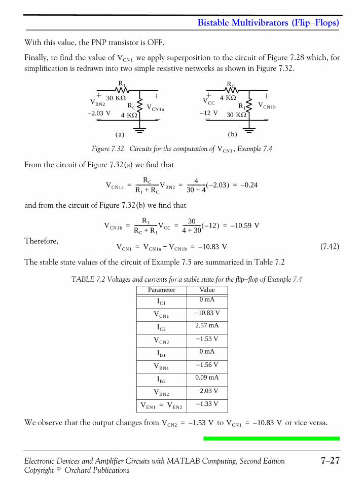
Electronic Devices and Amplifier Circuits with MATLAB Computing, Second Edition 7−27Copyright © Orchard Publications
Bistable Multivibrators (Flip−Flops)
With this value, the PNP transistor is OFF.
Finally, to find the value of we apply superposition to the circuit of Figure 7.28 which, forsimplification is redrawn into two simple resistive networks as shown in Figure 7.32.
Figure 7.32. Circuits for the computation of , Example 7.4
From the circuit of Figure 7.32(a) we find that
and from the circuit of Figure 7.32(b) we find that
Therefore,(7.42)
The stable state values of the circuit of Example 7.5 are summarized in Table 7.2
We observe that the output changes from to or vice versa.
TABLE 7.2 Voltages and currents for a stable state for the flip−flop of Example 7.4Parameter Value
0 mA
−10.83 V
2.57 mA
−1.53 V
0 mA
−1.56 V
0.09 mA
−2.03 V
−1.33 V
VCN1
RCR1
VBN2 VCN1aRC R1
30 KΩ4 KΩ
4 KΩVCC
2.03 V– 12– V
30 KΩVCN1b
a( ) b( )
VCN1
VCN1aRC
R1 RC+-------------------VBN2
430 4+--------------- 2.03–( ) 0.24–= = =
VCN1bR1
RC R1+-------------------VCC
304 30+--------------- 12–( ) 10.59 V–= = =
VCN1 VCN1a VCN1b+ 10.83 V–= =
IC1
VCN1
IC2
VCN2
IB1
VBN1
IB2
VBN2
VEN1 VEN2=
VCN2 1.53 V–= VCN1 10.83 V–=
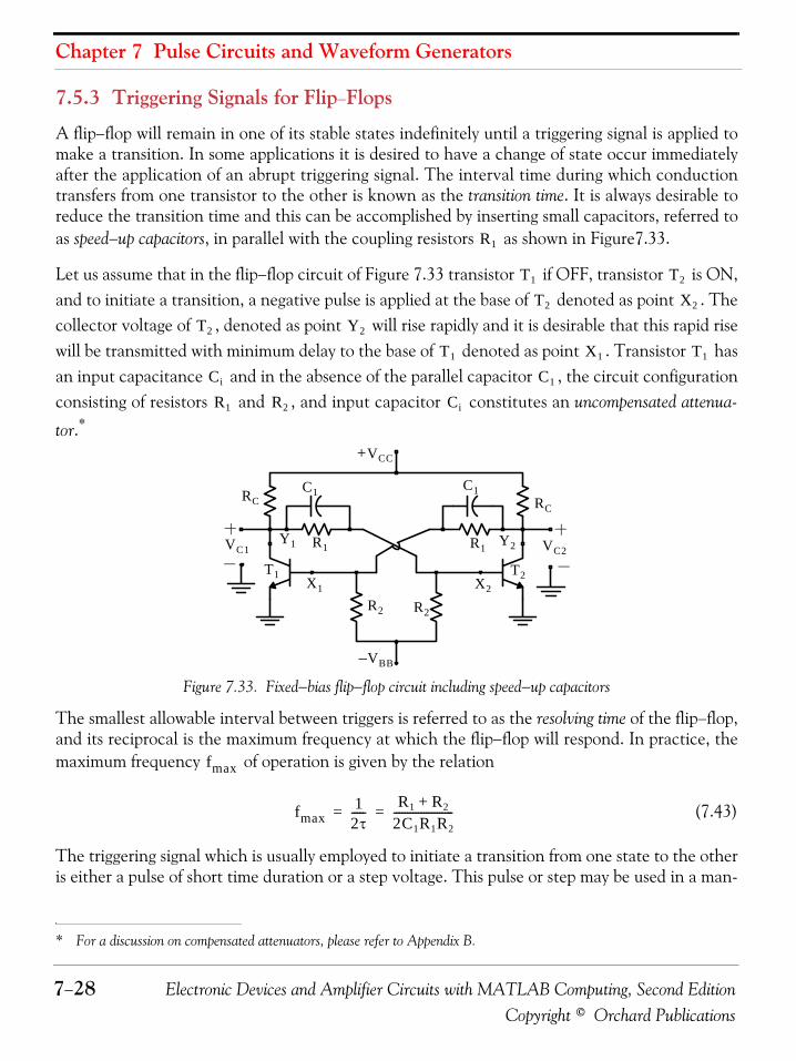
Chapter 7 Pulse Circuits and Waveform Generators
7−28 Electronic Devices and Amplifier Circuits with MATLAB Computing, Second EditionCopyright © Orchard Publications
7.5.3 Triggering Signals for Flip−Flops
A flip−flop will remain in one of its stable states indefinitely until a triggering signal is applied tomake a transition. In some applications it is desired to have a change of state occur immediatelyafter the application of an abrupt triggering signal. The interval time during which conductiontransfers from one transistor to the other is known as the transition time. It is always desirable toreduce the transition time and this can be accomplished by inserting small capacitors, referred toas speed−up capacitors, in parallel with the coupling resistors as shown in Figure7.33.
Let us assume that in the flip−flop circuit of Figure 7.33 transistor if OFF, transistor is ON,and to initiate a transition, a negative pulse is applied at the base of denoted as point . Thecollector voltage of , denoted as point will rise rapidly and it is desirable that this rapid risewill be transmitted with minimum delay to the base of denoted as point . Transistor hasan input capacitance and in the absence of the parallel capacitor , the circuit configurationconsisting of resistors and , and input capacitor constitutes an uncompensated attenua-
tor.*
Figure 7.33. Fixed−bias flip−flop circuit including speed−up capacitors
The smallest allowable interval between triggers is referred to as the resolving time of the flip−flop,and its reciprocal is the maximum frequency at which the flip−flop will respond. In practice, themaximum frequency of operation is given by the relation
(7.43)
The triggering signal which is usually employed to initiate a transition from one state to the otheris either a pulse of short time duration or a step voltage. This pulse or step may be used in a man-
* For a discussion on compensated attenuators, please refer to Appendix B.
R1
T1 T2
T2 X2
T2 Y2
T1 X1 T1
Ci C1
R1 R2 Ci
+VCC
V– BB
VC1
RC RC
R1 R1
T1
R2 R2
T2
C1
X2X1
VC2Y1 Y2
C1
fmax
fmax1
2τ----- R1 R2+
2C1R1R2----------------------= =
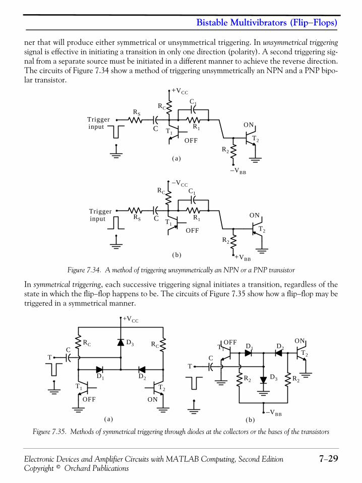
Electronic Devices and Amplifier Circuits with MATLAB Computing, Second Edition 7−29Copyright © Orchard Publications
Bistable Multivibrators (Flip−Flops)
ner that will produce either symmetrical or unsymmetrical triggering. In unsymmetrical triggeringsignal is effective in initiating a transition in only one direction (polarity). A second triggering sig-nal from a separate source must be initiated in a different manner to achieve the reverse direction.The circuits of Figure 7.34 show a method of triggering unsymmetrically an NPN and a PNP bipo-lar transistor.
Figure 7.34. A method of triggering unsymmetrically an NPN or a PNP transistor
In symmetrical triggering, each successive triggering signal initiates a transition, regardless of thestate in which the flip−flop happens to be. The circuits of Figure 7.35 show how a flip−flop may betriggered in a symmetrical manner.
Figure 7.35. Methods of symmetrical triggering through diodes at the collectors or the bases of the transistors
+VCC
a( )
V– BB
V– CC
+VBB
Trigger
b( )
T1
Trigger
input
input
T2
T1T2
OFF
ON
OFF
ON
RC
R1
R2
C1
C
RS
RS
C1
R1
RC
R2
C
D1
C
+VCC
V– BB
TT
C
a( ) b( )
T1
T2T1
T2
OFF
ONOFF
ON
RC
R2
D2RC
R2
D1
D2
D3
D3
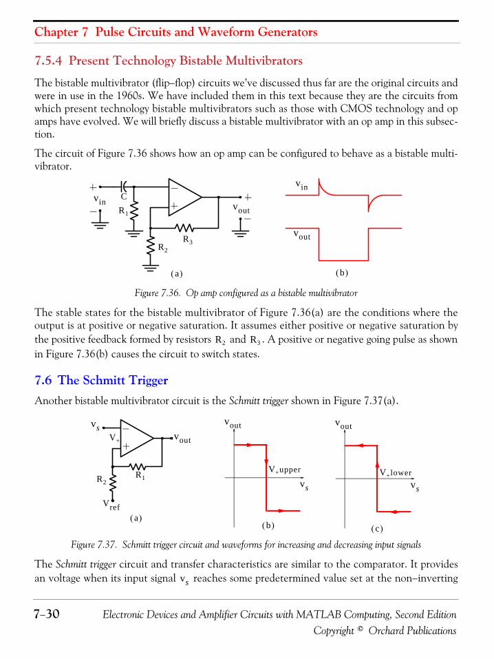
Chapter 7 Pulse Circuits and Waveform Generators
7−30 Electronic Devices and Amplifier Circuits with MATLAB Computing, Second EditionCopyright © Orchard Publications
7.5.4 Present Technology Bistable Multivibrators
The bistable multivibrator (flip−flop) circuits we’ve discussed thus far are the original circuits andwere in use in the 1960s. We have included them in this text because they are the circuits fromwhich present technology bistable multivibrators such as those with CMOS technology and opamps have evolved. We will briefly discuss a bistable multivibrator with an op amp in this subsec-tion.
The circuit of Figure 7.36 shows how an op amp can be configured to behave as a bistable multi-vibrator.
Figure 7.36. Op amp configured as a bistable multivibrator
The stable states for the bistable multivibrator of Figure 7.36(a) are the conditions where theoutput is at positive or negative saturation. It assumes either positive or negative saturation bythe positive feedback formed by resistors and . A positive or negative going pulse as shownin Figure 7.36(b) causes the circuit to switch states.
7.6 The Schmitt TriggerAnother bistable multivibrator circuit is the Schmitt trigger shown in Figure 7.37(a).
Figure 7.37. Schmitt trigger circuit and waveforms for increasing and decreasing input signals
The Schmitt trigger circuit and transfer characteristics are similar to the comparator. It providesan voltage when its input signal reaches some predetermined value set at the non−inverting
a( )
vin
b( )
vin
vout
voutR1
C
R3R2
R2 R3
vs
a( )
Vref
vout
R2R1
vout
vs
vout
vs
b( ) c( )
V +
V +upper V +lower
vs

Electronic Devices and Amplifier Circuits with MATLAB Computing, Second Edition 7−31Copyright © Orchard Publications
The Schmitt Trigger
input of the op amp. The output of the op amp changes from the positive saturation voltage to its negative saturation voltage and vice versa. As shown in Figure
7.37(b), the output is positively saturated as long as the input signal is less than the upper
threshold . If the input signal rises slightly above this threshold voltage, the output
drop abruptly to and stays there until drops below a lower threshold voltage
. The threshold voltages and are determined by the resistors and ,and the reference voltage . These threshold voltages can be found by application of KCL atthe non−inverting input of the op amp. Thus,
(7.44)
In (7.44), when is the maximum positive output voltage, , and when is
the maximum negative output voltage, .
Normally, the peak−to−peak output voltage of the Schmitt trigger of Figure 7.37 is often limitedby the use of back−to−back zeners across the output terminal and ground. The zener voltages arechosen so that the output swing from positive to negative or vice versa, is compatible with com-mercially available IC digital devices.
Example 7.6
For the Schmitt trigger circuit of Figure 7.38(a), the input signal is as shown in Figure 7.38(b).
Find and sketch and .
Solution:
It is given that the Schmitt trigger saturates positively at . Then, with (7.44)
Vout max( ) Vout max( )–
vs
V +upper vs
Vout max( )– vS
V +lower V +upper V +lower R1 R2
Vref
V + Vref–
R2----------------------
V + Vout–
R1------------------------+ 0=
1R1------ 1
R2------+⎝ ⎠
⎛ ⎞V +VoutR1
-----------VrefR2
----------+=
R1 R2+R1 R2⋅------------------⎝ ⎠
⎛ ⎞ V +⋅R1Vref R2Vout+
R1 R2⋅-----------------------------------------=
V +R1Vref R2Vout+
R1 R2+-----------------------------------------=
Vout V + V +upper= Vout
V + V +lower=
vs
V +upper V +lower
+12 V
V +upperR1Vref R2Vout+
R1 R2+----------------------------------------- 104 2 250 12×+×
10250--------------------------------------------- 2.24 V= = =
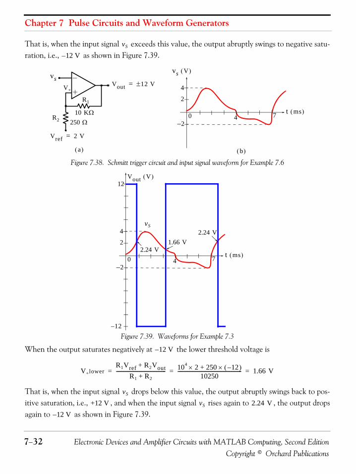
Chapter 7 Pulse Circuits and Waveform Generators
7−32 Electronic Devices and Amplifier Circuits with MATLAB Computing, Second EditionCopyright © Orchard Publications
That is, when the input signal exceeds this value, the output abruptly swings to negative satu-ration, i.e., as shown in Figure 7.39.
Figure 7.38. Schmitt trigger circuit and input signal waveform for Example 7.6
Figure 7.39. Waveforms for Example 7.3
When the output saturates negatively at the lower threshold voltage is
That is, when the input signal drops below this value, the output abruptly swings back to pos-itive saturation, i.e., , and when the input signal rises again to , the output dropsagain to as shown in Figure 7.39.
vS
12 V–
vs
a( )
Vref 2 V=
Vout 12 V±=
R2
R1
V +
t ms( )
vs V( )
2
7
4
42–
0
b( )
10 KΩ250 Ω
1.66 V
t ms( )
vS
2
7
4
42–
0
Vout V( )
12–
12
2.24 V
2.24 V
12 V–
V +lowerR1Vref R2Vout+
R1 R2+----------------------------------------- 104 2 250 12–( )×+×
10250----------------------------------------------------- 1.66 V= = =
vS
+12 V vS 2.24 V12 V–

Electronic Devices and Amplifier Circuits with MATLAB Computing, Second Edition 7−33Copyright © Orchard Publications
Summary
7.7 Summary• An astable multivibrator is essentially a digital clock which has two momentarily stable states
which alternate continuously producing square pulses.
• The 555 Timer circuit is a widely used IC for generating waveforms.
• A monostable multivibrator is an electronic circuit with two output states in which only onestate is stable. This circuit stays in its normal state until a signal is applied to its input. Whentriggered by an input signal, the output reverses states for a short period of time, dependingupon the circuit parameters. A monostable multivibrator is used primarily in pulse shapingapplications and to widen narrow pulses.
• Both astable and monostable multivibrators can constructed with a 555 timer circuit.
• IC device SN74121 is a popular monostable multivibrator where the time period that the out-put will stay High is determined by an external resistor and an external capacitor .
• A bistable multivibrator, commonly referred to as flip−flop, is an electronic circuits with twostable outputs one of which is the complement of the other. The outputs will change only whendirected by an input command.
• All three types of the multivibrators, i.e., astable, monostable, and bistable, can be constructedwith op amps employed as comparators.
• The Schmitt trigger is another bistable multivibrator circuit.
RX CX
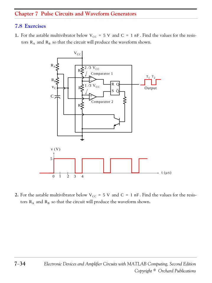
Chapter 7 Pulse Circuits and Waveform Generators
7−34 Electronic Devices and Amplifier Circuits with MATLAB Computing, Second EditionCopyright © Orchard Publications
7.8 Exercises
1. For the astable multivibrator below and . Find the values for the resis-tors and so that the circuit will produce the waveform shown.
2. For the astable multivibrator below and . Find the values for the resis-tors and so that the circuit will produce the waveform shown.
VCC 5 V= C 1 nF=
RA RB
RA
RB
C
vC
VCC
R
R
R
2 3⁄ VCC
1 3⁄ VCC
Comparator 1
Comparator 2
OutputR
S Q
Q
+
+
T1 T2
0 1 2
5
t μs( )
v V( )
3 4
VCC 5 V= C 1 nF=
RA RB

Electronic Devices and Amplifier Circuits with MATLAB Computing, Second Edition 7−35Copyright © Orchard Publications
Exercises
3. Repeat Exercise 2 to design a circuit that will produce the following waveform.
4. Design a monostable multivibrator using a 555 timer, a capacitor with value andappropriate resistor values to produce an output pulse of duration.
Output
T1 T2
VCC
RA
RB
vC
C
R
R
R
2 3⁄ VCC
1 3⁄ VCC
Comparator 1
Comparator 2
R
S Q
Q
+
+
0 1 2
5
t μs( )
v V( )
3 4 5
0 1 2
5
t μs( )
v V( )
3 4
C 1 nF=
20 μs

Chapter 7 Pulse Circuits and Waveform Generators
7−36 Electronic Devices and Amplifier Circuits with MATLAB Computing, Second EditionCopyright © Orchard Publications
5. The fixed−bias flip−flop circuit below is the same as that of Example 7.4.
The transistors are identical and the curves supplied by the manufacturer specify that and . Assume that the transistors have a minimum
value of 50. Using these voltages, recalculate the stable−state currents and voltages.
6. For the Schmitt trigger circuit of Figure (a) below, the input signal is as shown in Figure(b).
Find and sketch and .
12 V–
+12 V
2.2 KΩ15 KΩ
2.2 KΩ15 KΩ
VC2VC1
KΩ100 100
KΩ
T1 T2
VCE2 sat( ) 0.15 V= VBE2 sat( ) 0.7 V= hFE
vS
vs
a( )
Vref 1– V=
Vout 10 V±=
R2
R1
V +
ωt r( )
vs V( )
π 2⁄
b( )
40 KΩ
10 KΩ
5
0
5–
3π 2⁄π 2π
V +upper V +lower
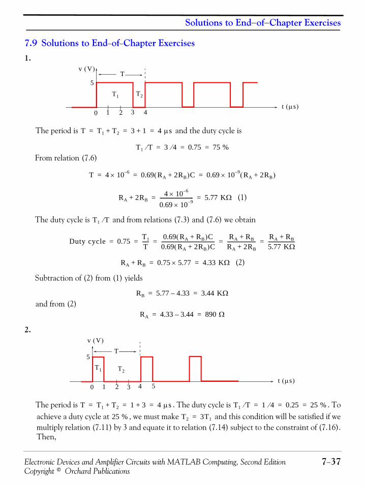
Electronic Devices and Amplifier Circuits with MATLAB Computing, Second Edition 7−37Copyright © Orchard Publications
Solutions to End−of−Chapter Exercises
7.9 Solutions to End−of−Chapter Exercises1.
The period is and the duty cycle is
From relation (7.6)
(1)
The duty cycle is and from relations (7.3) and (7.6) we obtain
(2)
Subtraction of (2) from (1) yields
and from (2)
2.
The period is . The duty cycle is . Toachieve a duty cycle at , we must make and this condition will be satisfied if wemultiply relation (7.11) by 3 and equate it to relation (7.14) subject to the constraint of (7.16).Then,
0 1 2
5
t μs( )
v V( )
3 4
T1
T
T2
T T1 T2+ 3 1+ 4 μs= = =
T1 T⁄ 3 4⁄ 0.75 75 %= = =
T 4 10 6–× 0.69 RA 2RB+( )C 0.69 10 9–× RA 2RB+( )= = =
RA 2RB+ 4 10 6–×0.69 10 9–×--------------------------- 5.77 KΩ= =
T1 T⁄
Duty cycle 0.75 T1
T----- 0.69 RA RB+( )C
0.69 RA 2RB+( )C------------------------------------------- RA RB+
RA 2RB+----------------------- RA RB+
5.77 KΩ----------------------= = = = =
RA RB+ 0.75 5.77× 4.33 KΩ= =
RB 5.77 4.33– 3.44 KΩ= =
RA 4.33 3.44– 890 Ω= =
0 1 2
5
t μs( )
v V( )
3 4 5
T
T1 T2
T T1 T2+ 1 3+ 4 μs= = = T1 T⁄ 1 4⁄ 0.25 25 %= = =
25 % T2 3T1=

Chapter 7 Pulse Circuits and Waveform Generators
7−38 Electronic Devices and Amplifier Circuits with MATLAB Computing, Second EditionCopyright © Orchard Publications
For convenience, we let and the relation above is written as
Therefore, let us plot the above relation with the following MATLAB script to find the x−axiszero crossing.
x=2.005:0.0001:2.006; y=3.*log(2).*(x+1)−log((2.*x−1)./(x−2)); plot(x,y);grid
The plot above indicates that the x−axis zero crossing occurs at approximately
and thus to achieve a duty cycle at , we should choose that the ratio should beclose to this value but not exactly equal or less than 2. The value of the capacitor can be
3 2RAClnRA RB⋅RA RB+--------------------C
2RA RB–RA 2RB–-----------------------⎝ ⎠
⎛ ⎞ln⋅=
RB
RA RB+-------------------- 2RA RB–
RA 2RB–-----------------------⎝ ⎠
⎛ ⎞ln⋅ 3 2ln=
3 2lnRA RB+
RB--------------------⎝ ⎠
⎛ ⎞⋅2RA RB–RA 2RB–-----------------------⎝ ⎠
⎛ ⎞ln=
3 2ln RA
RB------ 1+⎝ ⎠
⎛ ⎞⋅2RA RB⁄ 1–RA RB⁄ 2–
------------------------------⎝ ⎠⎛ ⎞ln=
x RA RB⁄=
3 2ln x 1+( )⋅ 2x 1–x 2–
---------------⎝ ⎠⎛ ⎞ln=
2.005 2.0052 2.0054 2.0056 2.0058 2.006-0.2
-0.15
-0.1
-0.05
0
0.05
x=RA/RB
T2=
3T1
x RA RB⁄ 2.0058= =
25 % RA RB⁄

Electronic Devices and Amplifier Circuits with MATLAB Computing, Second Edition 7−39Copyright © Orchard Publications
Solutions to End−of−Chapter Exercises
found from either expression (7.11) or (7.14) but (7.11) is simpler. We require that and assuming , we obtain
3.
The period is and the duty cycle is
Here, we must make and this condition will be satisfied if we multiply relation (7.14)by 3 and equate it to relation (7.11) subject to the constraint of (7.16). Then,
For convenience, we let and the relation above is written as
Therefore, let us plot above relation with the following MATLAB script to find the x−axis zerocrossing.
x=2.1:0.01:6; y=log(2).*(x+1)−3.*log((2.*x−1)./(x−2)); plot(x,y);grid
T1 1 μs=
RA 5.1 KΩ=
T1 10 6– 0.69RAC 0.69 5.1× 10³× C= = =
C 10 6–
0.69 5.1× 10³×-------------------------------------- 284 pF= =
0 1 2
5
t μs( )
v V( )
3 4
T
T1 T2
T T1 T2+ 3 1+ 4 μs= = =
T1 T⁄ 3 4⁄ 0.75 75 %= = =
T1 3T2=
2 RAC⋅ln 3RA RB⋅RA RB+--------------------C
2RA RB–RA 2RB–-----------------------⎝ ⎠
⎛ ⎞ln⋅ ⋅=
RB
RA RB+-------------------- 2RA RB–
RA 2RB–-----------------------⎝ ⎠
⎛ ⎞ln⋅ 2ln3
--------=
2ln3
-------- RA RB+RB
--------------------⎝ ⎠⎛ ⎞⋅
2RA RB–RA 2RB–-----------------------⎝ ⎠
⎛ ⎞ln=
2ln3
-------- RA
RB------ 1+⎝ ⎠
⎛ ⎞⋅2RA RB⁄ 1–RA RB⁄ 2–
------------------------------⎝ ⎠⎛ ⎞ln=
x RA RB⁄=
2ln x 1+( )⋅ 3 2x 1–x 2–
---------------⎝ ⎠⎛ ⎞ln=

Chapter 7 Pulse Circuits and Waveform Generators
7−40 Electronic Devices and Amplifier Circuits with MATLAB Computing, Second EditionCopyright © Orchard Publications
The plot above indicates that x−axis zero crossing occurs at approximately
and thus to achieve a duty cycle at , we should choose that the ratio should beclose to this value. The value of the capacitor can be found from either expression (7.11) or(7.14) but (7.11) is simpler. We require that and assuming , weobtain
Example 7.2 and Exercises 2 and 3 reveal that as the duty cycle decreases the ratio approaches the value of 2, and as the duty cycle increases, this ratio approaches the value of11.
4. We will use the monostable multivibrator of Figure 7.21 which is repeated below for conve-nience. From relation (7.28),
With a capacitor of value to produce an output pulse of duration, resis-tor must have the value of
2 2.5 3 3.5 4 4.5 5 5.5 6-10
-8
-6
-4
-2
0
2
x=RA/RB
T1=
3T2
x RA RB⁄ 4.25= =
75 % RA RB⁄
T1 3 μs= RA 5.1 KΩ=
T1 3 10 6–× 0.69RAC 0.69 5.1× 10³× C= = =
C 3 10 6–×0.69 5.1× 10³×-------------------------------------- 853 pF= =
RA RB⁄
T 1.1R1C≈
C 1 nF= T 20 μs=
R1
R1T
1.1C----------- 20 10 6–×
1.1 10 9–×------------------------ 18.2 KΩ= = =
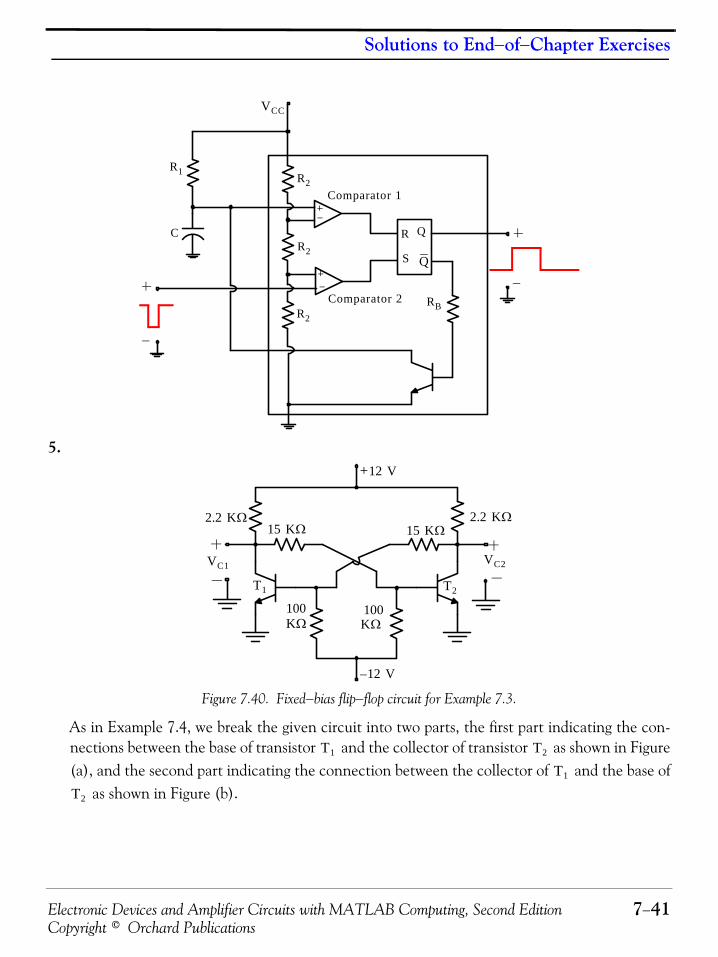
Electronic Devices and Amplifier Circuits with MATLAB Computing, Second Edition 7−41Copyright © Orchard Publications
Solutions to End−of−Chapter Exercises
5.
Figure 7.40. Fixed−bias flip−flop circuit for Example 7.3.
As in Example 7.4, we break the given circuit into two parts, the first part indicating the con-nections between the base of transistor and the collector of transistor as shown in Figure(a), and the second part indicating the connection between the collector of and the base of
as shown in Figure (b).
R1
VCC
R
Comparator 1
R2
R2
R2
RB
C
S
Q
Q
Comparator 2
12 V–
+12 V
2.2 KΩ15 KΩ
2.2 KΩ15 KΩ
VC2VC1
KΩ100 100
KΩ
T1 T2
T1 T2
T1
T2
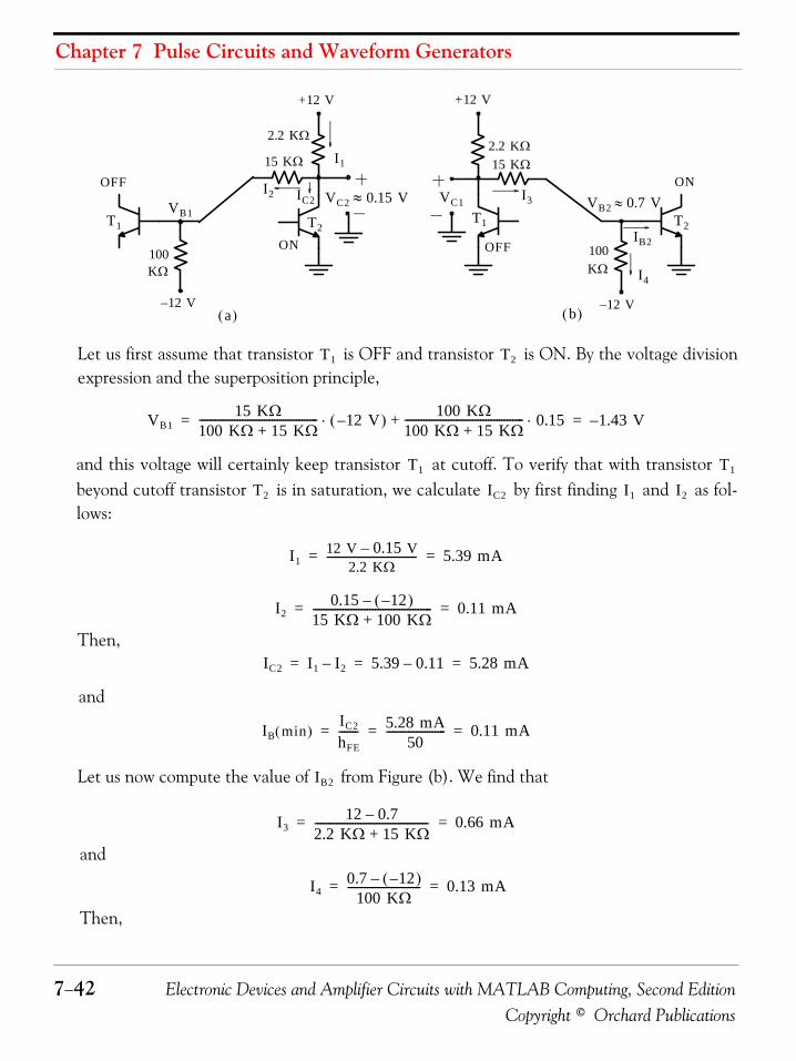
Chapter 7 Pulse Circuits and Waveform Generators
7−42 Electronic Devices and Amplifier Circuits with MATLAB Computing, Second EditionCopyright © Orchard Publications
Let us first assume that transistor is OFF and transistor is ON. By the voltage divisionexpression and the superposition principle,
and this voltage will certainly keep transistor at cutoff. To verify that with transistor beyond cutoff transistor is in saturation, we calculate by first finding and as fol-lows:
Then,
and
Let us now compute the value of from Figure (b). We find that
and
Then,
+12 V +12 V
12 V– 12 V–
T1 T2T1 T2
2.2 KΩ
15 KΩ 15 KΩ2.2 KΩ
100KΩ KΩ
100
VC2 0.15 V≈ VC1
OFF ON
ON OFF
VB2 0.7 V≈VB1IC2
I1
I2
IB2
I4
I3
a( ) b( )
T1 T2
VB115 KΩ
100 KΩ 15 KΩ+-------------------------------------------- 12 V–( )⋅ 100 KΩ
100 KΩ 15 KΩ+-------------------------------------------- 0.15⋅+ 1.43 V–= =
T1 T1
T2 IC2 I1 I2
I112 V 0.15 V–
2.2 KΩ--------------------------------- 5.39 mA= =
I20.15 12–( )–
15 KΩ 100 KΩ+-------------------------------------------- 0.11 mA= =
IC2 I1 I2– 5.39 0.11– 5.28 mA= = =
IB min( )IC2
hFE------- 5.28 mA
50---------------------- 0.11 mA= = =
IB2
I312 0.7–
2.2 KΩ 15 KΩ+------------------------------------------ 0.66 mA= =
I40.7 12–( )–
100 KΩ--------------------------- 0.13 mA= =
Electronic Devices and Amplifier Circuits with MATLAB Computing, Second Edition 7−43Copyright © Orchard Publications
Solutions to End−of−Chapter Exercises
Since , that is, the value of exceeds the minimumbase current value of required for saturation, we have shown that transistor isdeeply into saturation.
Finally, the collector voltage if found from Figure (b) as
and this value is close to the collector supply voltage of 12 volts.
Therefore, with the values given the more accurate voltages and currents for a stable state forthe flip−flop of this example are summarized in the table below.
A comparison of the values of Table 7.1 and those of the table above reveals that the error inassuming that a transistor in saturation behaves as an ideal short circuit is very small and thiserror can be neglected.
The second stable state is the one in which transistor is ON and transistor is OFF. Theanalysis is the same as above where the voltages and currents are interchanged between tran-sistors and , and .
Parameter Value0 mA
10.5 V
5.28 mA
0.15 V
0 mA
−1.43 V
0.53 mA
0.7 V
IB2 I3 I4– 0.66 0.13– 0.53 mA= = =
IB2 0.53 mA=( ) IB min( ) 0.11 mA=( )> IB2
IB min( ) T2
VC1
VC1 12 2.2 103× I3×– 12 2.2 103× 0.66 10 3–××– 10.5 V= = =
IC1
VC1
IC2
VC2
IB1
VB1
IB2
VB2
T1 T2
T1 T2 VC2 10.5 V=
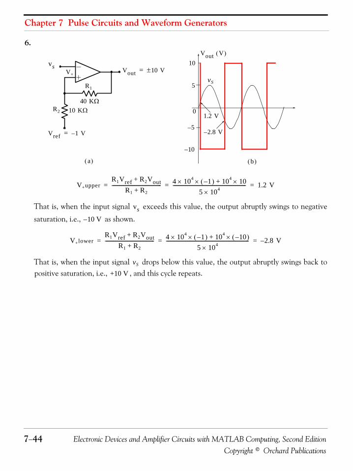
Chapter 7 Pulse Circuits and Waveform Generators
7−44 Electronic Devices and Amplifier Circuits with MATLAB Computing, Second EditionCopyright © Orchard Publications
6.
That is, when the input signal exceeds this value, the output abruptly swings to negative
saturation, i.e., as shown.
That is, when the input signal drops below this value, the output abruptly swings back topositive saturation, i.e., , and this cycle repeats.
vs
a( )
Vref 1– V=
Vout 10 V±=
R2
R1
V +vS
5–
10–
0
b( )
40 KΩ10 KΩ
5
10Vout V( )
2.8– V
1.2 V
V +upperR1Vref R2Vout+
R1 R2+----------------------------------------- 4 10× 4 1–( ) 104 10×+×
5 10× 4------------------------------------------------------------- 1.2 V= = =
vs
10 V–
V +lowerR1Vref R2Vout+
R1 R2+----------------------------------------- 4 10× 4 1–( ) 104 10–( )×+×
5 10× 4--------------------------------------------------------------------- 2.8– V= = =
vS
+10 V
Electronic Devices and Amplifier Circuits with MATLAB Computing, Second Edition 8−1Copyright © Orchard Publications
Chapter 8
Frequency Characteristics of Single−Stage and Cascaded Amplifiers
his chapter presents certain basic concepts and procedures that are applicable to frequencydependent single−stage and cascaded amplifiers. The intent is to provide the basic principlesof the frequency dependence that is an essential prerequisite for the effective design and uti-
lization of most electronic circuits.
8.1 Properties of Signal WaveformsIn the study of electronic systems we encounter an extremely wide variety of signal waveforms.The simplest are sinusoidal with frequencies of or but in most cases we are con-cerned with a more complicated class of periodic but non−sinusoidal waveforms. For these wave-forms we attempt to represent the signals as a superposition of sinusoidal components of appropri-ate amplitudes, frequencies, and phases. Fortunately, very powerful techniques for this purpose areavailable such as the Fourier series,* Fourier transform, and the Laplace transformation.
Periodic signals can be represented as the superposition of sinusoidal components by a Fourierseries of the form
(8.1)
where is the DC component of the composite signal, is the fundamental frequency or first har-monic, , is the second harmonic, is the third harmonic, and so on.
Unfortunately, not all signals consist of harmonically related components. In the case of speech ormusic, for instance, the sinusoidal composition of the sound is continuously changing. In this case,the composite signal can be approximated by the superposition of a number of sinusoidal compo-nents expressed as
(8.2)
where is the DC component of the composite signal, and , , , and so on, are not har-monically related.
Figure 8.1, referred to as the frequency spectrum of the signal reveals information about the fre-quencies and amplitude, but it contains no information about the phase angles of the components.
* For a thorough discussion on Fourier series, the Fourier transform, and the Laplace transformation please referto Signals and Systems with MATLAB Computing and Simulink Modeling, ISBN 978−1−934404−11−9.
T
60 Hz 400 Hz
v t( ) V V1 ωt θ1+( )cos V2 2ωt θ2+( )cos V3 3ωt θ3+( ) …+cos+ + +=
V ω2ω 3ω
v t( ) V V1 ω1t θ1+( )cos V2 ω2t θ2+( )cos V3 ω3t θ3+( ) …+cos+ + +=
V ω1 ω2 ω3

Frequency Characteristics of Single−Stage and Cascaded Amplifiers
8−2 Electronic Devices and Amplifier Circuits with MATLAB Computing, Second EditionCopyright © Orchard Publications
Figure 8.1. Typical frequency spectrum
The frequency spectrum of Figure 8.1 represents the square waveform shown in Figure 8.2.*
Figure 8.2. Waveform that produces the frequency spectrum in Figure 8.1
Example 8.1 The frequency components of the frequency spectrum of Figure 8.1 are as shown in relation (8.3)below.
(8.3)
What percentage of the average power is absorbed by
a. the fundamental frequency
b. the fundamental and the third harmonic
c. the fundamental, the third, and the fifth harmonicSolution:
The instantaneous power is and for simplicity let us assume that . The averagepower over a period is
(8.4)
We recall that the RMS value of a sinusoid is the amplitude of the sinusoid divided by . Thus,
* Please refer to Chapter 7, Signals and Systems with MATLAB Computing and Simulink Modeling, ISBN978−1−934404−11−9.
bn
nωt0 1 3 5 7 9
4A/π
4A/3π 4A/5π 4A/7π 4A/9π
TA
0 π 2πωt
v t( ) 4Aπ
------- ωt 13--- 3ωt 1
5--- 5ωtsin …+ +sin+sin⎝ ⎠
⎛ ⎞ 4Aπ
------- 1n--- nωtsin
n odd=
∑= =
p v2 R⁄= R 1=
P T
P 1T--- v2 td
0
T
∫1T---v2t
0
T
v2= = =
2

Electronic Devices and Amplifier Circuits with MATLAB Computing, Second Edition 8−3Copyright © Orchard Publications
Properties of Signal Waveforms
the average power in the harmonics of relation (8.3) is
a. Percentage of power absorbed by the fundamental frequency component:
b. Percentage of power absorbed by the fundamental frequency and the third harmonic compo-nents:
c. Percentage of power absorbed by the fundamental frequency, the third, and the fifth harmoniccomponents:
This example indicates that most of the power is absorbed by the fundamental frequency and thefirst two non−zero harmonics. Of course, the power absorbed would be considerably higher if thesignal would include a DC component.
Figure 8.3 shows a typical curve of amplification versus frequency.
Figure 8.3. Typical frequency characteristics of an amplifier
As shown in Figure 8.3, the amplification decreases at high frequencies as a result of the parasiticcapacitances in the circuit, and decreases at low frequencies because of the presence of couplingcapacitors. Also, for a good designed amplifier, the amplification near the lower and near thehigher band of frequencies should not be less than 70 percent of the amplification in the middle ofthe band. It turns out that if an amplifier retards the phase of each sinusoidal component of thesignal in direct proportion to the frequency of that component, then the waveform of the outputsignal is an exact copy of the input waveform, but it is delayed in time. This can be illustrated byexpressing relation (8.2) with the introduction of a constant time delay . Then,
P1 P3 P5 …+ + + V12 V3
2 V52 …+ + +
4A2π
---------- 1⋅⎝ ⎠⎛ ⎞ 2 4A
2π---------- 1
3---⋅⎝ ⎠
⎛ ⎞ 2 4A2π
---------- 15---⋅⎝ ⎠
⎛ ⎞ 2…+ + += =
8A2
π2--------- 1 1
9--- 1
25------ …+ + +⎝ ⎠
⎛ ⎞=
8π2----- 1⋅⎝ ⎠
⎛ ⎞ 100× 81%=
8π2----- 1 1
9---+⎝ ⎠
⎛ ⎞⋅ 100× 90%=
8π2----- 1 1
9--- 1
25------+ +⎝ ⎠
⎛ ⎞⋅ 100× 93%=
T
v t T–( ) V V1 ω1 t T–( ) θ1+( )cos V2 ω2 t T–( ) θ2+( )cos V3 ω3 t T–( ) θ3+( ) …+cos+ + +=

Frequency Characteristics of Single−Stage and Cascaded Amplifiers
8−4 Electronic Devices and Amplifier Circuits with MATLAB Computing, Second EditionCopyright © Orchard Publications
Letting we obtain
(8.5)
Relation (8.5) reveals that the introduction of a constant delay adds a phase lag to each com-ponent, directly proportional to the frequency of that component. Reversing the above processwe can see that if an amplifier introduces a phase lag that increases linearly with frequency, then
, and the amplifier produces a time delay , and if the amplification is the same forall frequencies, the signal is not distorted; it is merely delayed in time. In conclusion, the analysisand design of linear amplifiers is concerned with the characteristics of amplification and phaseshift versus frequency.
For the remaining of this chapter and Chapter 9, we will develop procedures for constructingthese characteristics. Subsequently, an easy method to begin with the design of amplifiers at low,medium, and high frequencies is to first define the transfer function gain and the frequen-cies as the poles of the transfer function and draw the Bode plot using MATLAB.*
The results of the following example will be useful in our analysis and development of equivalentcircuits.
Example 8.2 Prove that the circuits of Figure 8.4(a) and 8.4(b) are equivalent.
Figure 8.4. Equivalent circuits for Example 8.2
* Frequency response and Bode plots are discussed in detail in Circuit Analysis II with MATLAB Applications,ISBN 978−0−9709511−5−1.
φ k ω kT=
v t T–( ) V V1 ω1t φ1– θ1+( )cos V2 ω2t φ2– θ2+( )cos V3 ω3t φ3– θ3+( ) …+cos+ + +=
φ k
φ Kω= T K=
G s( )
vin
vg
R1R2
R3
R4
R1 R2
R3
R4
vg
gmvg
gmvg gmvg
vout
v1 v2
vin
vout
v1 v2
a( )
b( )

Electronic Devices and Amplifier Circuits with MATLAB Computing, Second Edition 8−5Copyright © Orchard Publications
The Transistor Amplifier at Low Frequencies
Proof:
Application of KCL at and of Figure 8.4(a) yields
(8.6)
Application of KCL at and of Figure 8.4(b) yields
(8.7)
We observe that equations (8.6) and (8.7) are the same and thus the circuits of Figures 8.4(a) and8.4(b) are equivalent.
8.2 The Transistor Amplifier at Low FrequenciesFigure 8.5 shows a transistor amplifier and its equivalent circuits that can be used as a low fre-quency amplifier.
Figure 8.5. Transistor amplifier and equivalent circuits at low frequencies
The behavior of the amplifier of Figure 8.5(a) at low frequencies is affected by the action of capac-itor . An incremental model for the amplifier that is valid at low and medium frequencies is
v1 v2
v1
R2------ v1 v2–
R3---------------- gmvg–+ 0=
v2 v1–R3
---------------- v2
R4------ gmvg+ + 0=
v1 v2
v1
R2------ gmvg–
v1 v2–R3
----------------+ 0=
v2 v1–R3
---------------- gmvgv2
R4------+ + 0=
RA
RB
R2
C3
R2
R3
VCC
R2
I2
I1
IBR1
rn
βIB
R3 C3
rn
IB
βIB R3C3 βIB
R2
I2
R1R1
I1
I1 IB
rn
I2βIB1 β+( )R3
C3
1 β+( )----------------
a( )
b( )
c( ) d( )
vin
vin
vin vin
C3
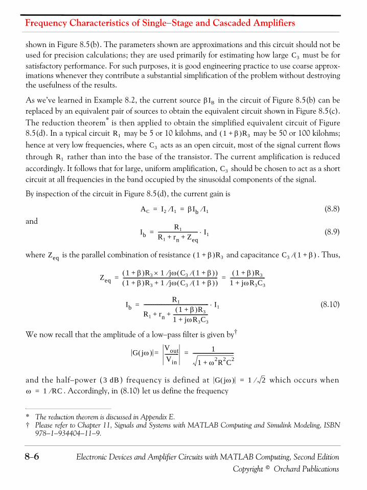
Frequency Characteristics of Single−Stage and Cascaded Amplifiers
8−6 Electronic Devices and Amplifier Circuits with MATLAB Computing, Second EditionCopyright © Orchard Publications
shown in Figure 8.5(b). The parameters shown are approximations and this circuit should not beused for precision calculations; they are used primarily for estimating how large must be forsatisfactory performance. For such purposes, it is good engineering practice to use coarse approx-imations whenever they contribute a substantial simplification of the problem without destroyingthe usefulness of the results.
As we’ve learned in Example 8.2, the current source in the circuit of Figure 8.5(b) can bereplaced by an equivalent pair of sources to obtain the equivalent circuit shown in Figure 8.5(c).The reduction theorem* is then applied to obtain the simplified equivalent circuit of Figure8.5(d). In a typical circuit may be 5 or 10 kilohms, and may be 50 or 100 kilohms;hence at very low frequencies, where acts as an open circuit, most of the signal current flowsthrough rather than into the base of the transistor. The current amplification is reducedaccordingly. It follows that for large, uniform amplification, should be chosen to act as a shortcircuit at all frequencies in the band occupied by the sinusoidal components of the signal.
By inspection of the circuit in Figure 8.5(d), the current gain is
(8.8)and
(8.9)
where is the parallel combination of resistance and capacitance . Thus,
(8.10)
We now recall that the amplitude of a low−pass filter is given by†
and the half−power ( ) frequency is defined at which occurs when. Accordingly, in (8.10) let us define the frequency
* The reduction theorem is discussed in Appendix E.† Please refer to Chapter 11, Signals and Systems with MATLAB Computing and Simulink Modeling, ISBN
978−1−934404−11−9.
C3
βIB
R1 1 β+( )R3
C3
R1
C3
AC I2 I1⁄ βIb I1⁄= =
IbR1
R1 rn Zeq+ +-------------------------------- I1⋅=
Zeq 1 β+( )R3 C3 1 β+( )⁄
Zeq1 β+( )R3 1 jω C3 1 β+( )⁄( )⁄×1 β+( )R3 1 jω C3 1 β+( )⁄( )⁄+
---------------------------------------------------------------------------- 1 β+( )R3
1 jωR3C3+----------------------------= =
IbR1
R1 rn1 β+( )R3
1 jωR3C3+----------------------------+ +
---------------------------------------------------- I1⋅=
G jω( )VoutVin-----------= 1
1 ω2R2C2+---------------------------------=
3 dB G jω( ) 1 2⁄=
ω 1 RC⁄=

Electronic Devices and Amplifier Circuits with MATLAB Computing, Second Edition 8−7Copyright © Orchard Publications
The Transistor Amplifier at Low Frequencies
(8.11)
Factoring out of the denominator in (8.10) and multiplying both numerator and denomi-
nator by , we obtain
(8.12)
and with (8.8) we find that the current gain is given by
(8.13)
In the medium−frequency range the term is very large, and the second factor on the rightside in (8.13) approaches unity; hence the first factor is the current gain at medium frequencies.Relation (8.13) can be expressed in a more convenient form by defining two new terms as
(8.14)
and(8.15)
Substitution of (8.14) and (8.15) in (8.13) and factoring out the denominator yields
(8.16)
Relation (8.16) can be used as a guide in the design of transistor amplifiers for low−frequencyresponses once the quiescent operating point has been established. The bypass capacitor is thenchosen to make the break in the amplitude characteristic at occur at a suitablepoint below the band of frequencies occupied by the signal. Changing the value of does notchange the shape of the ramp in the amplitude characteristic; it only shifts the ramp parallel to thefrequency axis.
Example 8.3
For the transistor amplifier in Figure 8.5, it is known that , , ,
, and . Construct the logarithmic amplitude characteristic for this amplifier inthe low− and medium−frequency range.
ω3 1 R3C3⁄=
R1 rn+
1 jω ω3⁄+
IbR1I1
R1 rn+----------------- 1 jω ω3⁄+
1 1 β+( )R3
R1 rn+------------------------ jω
ω3------+ +
----------------------------------------------⋅=
ACI2
I1----
βIbI1
--------βR1
R1 rn+----------------- 1 jω ω3⁄+
1 1 β+( )R3
R1 rn+------------------------ jω
ω3------+ +
----------------------------------------------⋅= = =
ω ω3⁄
AmβR1
R1 rn+-----------------=
k31 β+( )R3
R1 rn+------------------------=
1 k3+
AC
Am1 k3+-------------- 1 jω ω3⁄+
1 jω 1 k3+( )ω3⁄+---------------------------------------------⋅=
ω 1 k3+( )ω3=
C3
R1 3 KΩ= rn 12 KΩ= R3 1 KΩ=
β 80= C3 2.5 μF=

Frequency Characteristics of Single−Stage and Cascaded Amplifiers
8−8 Electronic Devices and Amplifier Circuits with MATLAB Computing, Second EditionCopyright © Orchard Publications
Solution:The amplification at medium frequencies is given by (8.40). Thus
and in decibels
The break frequency in (8.16) is
or
The factor is found from (8.15), that is,
and the break frequency for the factor in the denominator of relation (8.16) is
or
The amount by which the amplification at low frequencies is less than its value at medium fre-quencies is
Therefore, from DC to the break frequency at , the gain is . The amplitudecharacteristic is shown in Figure 8.6 where the frequency is shown in logarithmic scale and thegain is in scale.
Figure 8.6. Amplitude characteristic for the amplifier of Example 8.3
AmβR1
R1 rn+----------------- 80 3×
3 12+--------------- 18= = =
Am dB( ) 20 18log 20 1.25× 25 dB= = =
ω3
ω31
R3C3------------ 1
1000 2.5 10 6–××------------------------------------------ 400 rad/sec= = =
f3ω3
2π------ 400
2π--------- 64 Hz≈= =
k3
k31 β+( )R3
R1 rn+------------------------ 1 80+( ) 1×
3 12+----------------------------- 5.4= = =
1 k3+( )ω3
1 k3+( )ω3 1 5.4+( ) 400× 2560 rad/sec= =
1 k3+( )f3 1 5.4+( ) 64× 410 Hz= =
20 1 k3+( )log 20 0.8× 16 dB= =
64 Hz 25 16– 9 dB=
dB
10
20
30
f Hz( )0
1 10 100 1000
Gain dB( )
64 Hz 410 Hz
1 k3+( )f3
f3
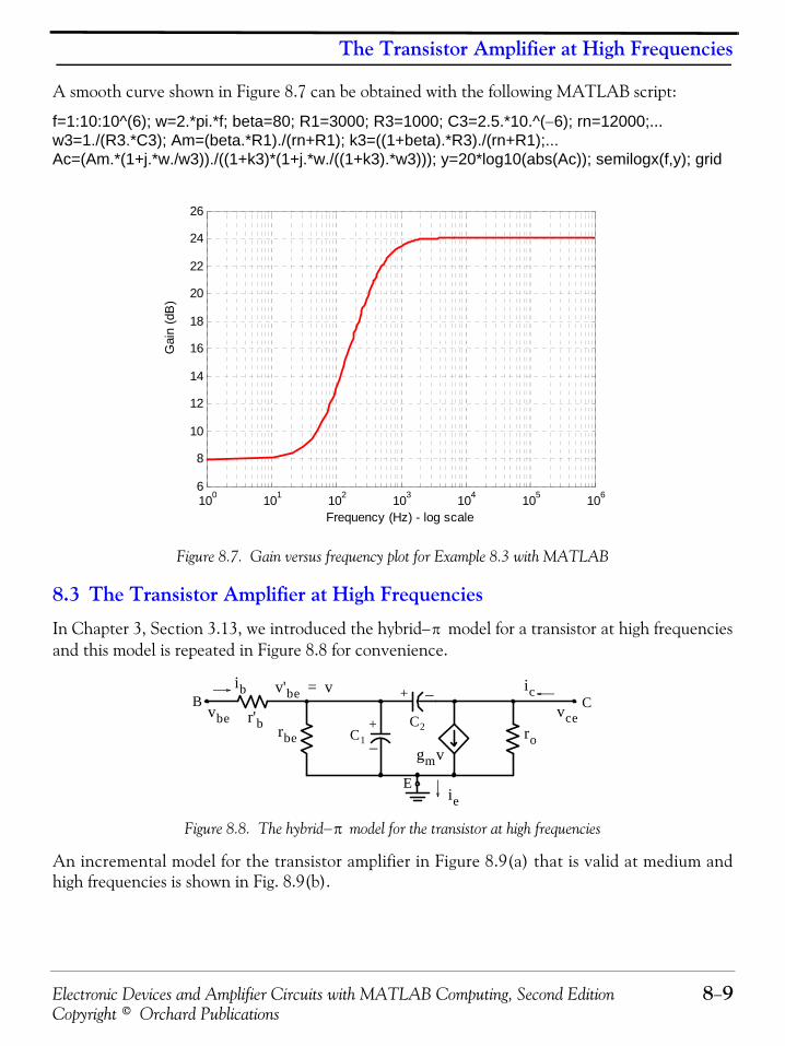
Electronic Devices and Amplifier Circuits with MATLAB Computing, Second Edition 8−9Copyright © Orchard Publications
The Transistor Amplifier at High Frequencies
A smooth curve shown in Figure 8.7 can be obtained with the following MATLAB script:
f=1:10:10^(6); w=2.*pi.*f; beta=80; R1=3000; R3=1000; C3=2.5.*10.^(−6); rn=12000;...w3=1./(R3.*C3); Am=(beta.*R1)./(rn+R1); k3=((1+beta).*R3)./(rn+R1);...Ac=(Am.*(1+j.*w./w3))./((1+k3)*(1+j.*w./((1+k3).*w3))); y=20*log10(abs(Ac)); semilogx(f,y); grid
Figure 8.7. Gain versus frequency plot for Example 8.3 with MATLAB
8.3 The Transistor Amplifier at High Frequencies
In Chapter 3, Section 3.13, we introduced the hybrid− model for a transistor at high frequenciesand this model is repeated in Figure 8.8 for convenience.
Figure 8.8. The hybrid− model for the transistor at high frequencies
An incremental model for the transistor amplifier in Figure 8.9(a) that is valid at medium andhigh frequencies is shown in Fig. 8.9(b).
100
101
102
103
104
105
106
6
8
10
12
14
16
18
20
22
24
26
Frequency (Hz) - log scale
Gai
n (d
B)
π
rbe
Bib
vbero
gmv
E
icvce
C
ie
r'b
v'be v=
+
−
C1
C2
+
−
π
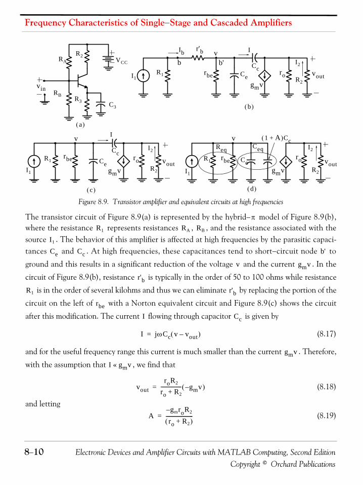
Frequency Characteristics of Single−Stage and Cascaded Amplifiers
8−10 Electronic Devices and Amplifier Circuits with MATLAB Computing, Second EditionCopyright © Orchard Publications
Figure 8.9. Transistor amplifier and equivalent circuits at high frequencies
The transistor circuit of Figure 8.9(a) is represented by the hybrid− model of Figure 8.9(b),where the resistance represents resistances , , and the resistance associated with thesource . The behavior of this amplifier is affected at high frequencies by the parasitic capaci-tances and . At high frequencies, these capacitances tend to short−circuit node to
ground and this results in a significant reduction of the voltage and the current . In the
circuit of Figure 8.9(b), resistance is typically in the order of 50 to 100 ohms while resistance
is in the order of several kilohms and thus we can eliminate by replacing the portion of the
circuit on the left of with a Norton equivalent circuit and Figure 8.9(c) shows the circuit
after this modification. The current flowing through capacitor is given by
(8.17)
and for the useful frequency range this current is much smaller than the current . Therefore,
with the assumption that , we find that
(8.18)
and letting(8.19)
RA
RB
C3
R2
R3
VCC
R2
I2
gmv
1 A+( )Cc
a( )
b( )
c( ) d( )
roCc
Ce
v
rbeR1
I1
Req Ceq
I
gmv
v
roR2
I2
CerbeR1
I1
vout
I1R1 rbe
I
voutroR2
I2
gmv
Cc
Ib v
Ce
r'bb'b
vin
vout
πR1 RA RB
I1
Ce Cc b'
v gmv
r'bR1 r'b
rbe
I Cc
I jωCc v vout–( )=
gmv
I gmv«
voutroR2
ro R2+----------------- gmv–( )=
Agm– roR2
ro R2+( )----------------------=

Electronic Devices and Amplifier Circuits with MATLAB Computing, Second Edition 8−11Copyright © Orchard Publications
The Transistor Amplifier at High Frequencies
we obtain(8.20)
Typically, the gain in (8.20) is in the range of 10 to 1000. Also, , and thus .Therefore, we can express (8.17) as
(8.21)
This relation enable us to replace the current by a capacitor of the value as shown inFigure 8.9(d), and as we know from Appendix C, this amplifying property of the transistor whichincreases the apparent value of the collector capacitance is known as the Miller effect.
From the circuit of Figure 8.9(d),
(8.22)
(8.23)
(8.24)
(8.25)
The current gain is now found by division of (8.22) by (8.25). Thus,
(8.26)
Next, we let(8.27)
and we define the half−power ( ) frequency as
(8.28)
Substitution of (8.27) and (8.28) into (8.26) yields
(8.29)
At medium frequencies is small, that is, , and the second factor on the right side in
vout Av–=
A ro R2» A gmR2≈
I jωCc v Av+( ) jωCc 1 A+( )v jωCcAv≈= =
I 1 A+( )Cc
I2
roro R2+-----------------gmv=
Ceq Ce 1 A+( )Cc+=
ReqrbeR1
rbe R1+-------------------=
v1 jωCeq⁄
Req 1 jωCeq⁄+-------------------------------------- I1⋅
⎝ ⎠⎜ ⎟⎛ ⎞
ReqReq
1 jωReqCeq+---------------------------------- I1⋅= =
Ac
AcI2
I1----
roro R2+-----------------
gmReq1 jωReqCeq+----------------------------------⋅= =
Amro
ro R2+-----------------gmReq=
3 dB
ω11
ReqCeq------------------=
Ac Am1
1 jω ω1⁄+-------------------------=
ω ω ω1«
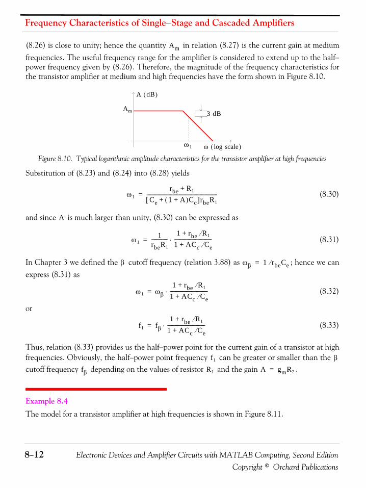
Frequency Characteristics of Single−Stage and Cascaded Amplifiers
8−12 Electronic Devices and Amplifier Circuits with MATLAB Computing, Second EditionCopyright © Orchard Publications
(8.26) is close to unity; hence the quantity in relation (8.27) is the current gain at mediumfrequencies. The useful frequency range for the amplifier is considered to extend up to the half−power frequency given by (8.26). Therefore, the magnitude of the frequency characteristics forthe transistor amplifier at medium and high frequencies have the form shown in Figure 8.10.
Figure 8.10. Typical logarithmic amplitude characteristics for the transistor amplifier at high frequencies
Substitution of (8.23) and (8.24) into (8.28) yields
(8.30)
and since is much larger than unity, (8.30) can be expressed as
(8.31)
In Chapter 3 we defined the cutoff frequency (relation 3.88) as ; hence we canexpress (8.31) as
(8.32)
or
(8.33)
Thus, relation (8.33) provides us the half−power point for the current gain of a transistor at highfrequencies. Obviously, the half−power point frequency can be greater or smaller than the cutoff frequency depending on the values of resistor and the gain .
Example 8.4 The model for a transistor amplifier at high frequencies is shown in Figure 8.11.
Am
A dB( )
3 dB
ω1
Am
ω scalelog( )
ω1rbe R1+
Ce 1 A+( )Cc+[ ]rbeR1---------------------------------------------------------=
A
ω11
rbeR1-------------
1 rbe R1⁄+
1 ACc Ce⁄+------------------------------⋅=
β ωβ 1 rbeCe⁄=
ω1 ωβ1 rbe R1⁄+
1 ACc Ce⁄+------------------------------⋅=
f1 fβ1 rbe R1⁄+
1 ACc Ce⁄+------------------------------⋅=
f1 β
fβ R1 A gmR2=

Electronic Devices and Amplifier Circuits with MATLAB Computing, Second Edition 8−13Copyright © Orchard Publications
The Transistor Amplifier at High Frequencies
Figure 8.11. Model of the transistor amplifier for Example 8.6
For this circuit it is known that , , the quiescent collector current is, , , , , and the current gain−bandwidth fre-
quency is . Determine:
a. the Miller effect at high frequencies
b. the medium frequency current amplification
c. the half−power frequency
Solution:
Since and , the given model circuit can be simplified to that shown in Figure 8.12.
Figure 8.12. Simplified model of the transistor amplifier for Example 8.6
From Chapter 3, relation (3.78),
From relation (3.83),
and from (3.92),
This indicates that large current amplification is provided at frequencies up to .
From (3.93),
I1
R1 rbe voutro
R2
I2
gmv
Cc
v
Ce
r'b b'b
R1 5 KΩ= R2 1 KΩ=
IC 5 mA= β 80= r'b 50 Ω= Cc 3 pF= ro 50 KΩ=
fT 400 MHz=
1 A+( )Cc
Am
f1
R1 r'b» ro R2»
Cc
gmvR2
I2
CerbeR1
I1
gm 40IC 40 5 10 3–×× 0.2 Ω 1–= = =
rbeβ
gm------- 80
0.2------- 400 Ω= = =
fβfT
β---- 400
80--------- 5 MHz= = =
5 MHz
Cegm
ωT------ 0.2
2π 4 108××------------------------------ 79.6 pF= = =

Frequency Characteristics of Single−Stage and Cascaded Amplifiers
8−14 Electronic Devices and Amplifier Circuits with MATLAB Computing, Second EditionCopyright © Orchard Publications
a. The Miller effect is where
Thus,
and this indicates that the dominant effect at high frequencies is the Miller effect.
b. From Figure 8.12,
and the medium frequency current amplification is given by (8.27) as
and since ,
This value is close to the value of of the transistor and thus it is near the maximum valuethat can be obtained by this transistor.
c. The half−power frequency is found from (8.33). Then,
8.4 Combined Low− and High−Frequency CharacteristicsThe frequency dependence of various amplifier circuits is examined by treating the low−fre-quency characteristics separately from the high−frequency characteristics. However, the com-bined low− and high−frequency characteristics can be displayed on a single set of coordinates asshown in Figure 8.13
1 A+( )Cc
A gmR2 0.2 1000× 200= = =
1 A+( )Cc 201 3 10 12–×× 603 10 12–× 603 pF= = =
ReqrbeR1
rbe R1+------------------- 400 5 103××
5.4 103×-------------------------------- 370 Ω= = =
Am
Amro
ro R2+-----------------gmReq=
ro R2»Am gmReq≈ 0.2 370× 74= =
β
f1
f1 fβ1 rbe R1⁄+
1 ACc Ce⁄+------------------------------⋅ 5 106× 1 400 5000⁄+
1 200 3 10 12–× 80 10 12–×( )⁄×+------------------------------------------------------------------------------- 0.635 MHz=⋅= =
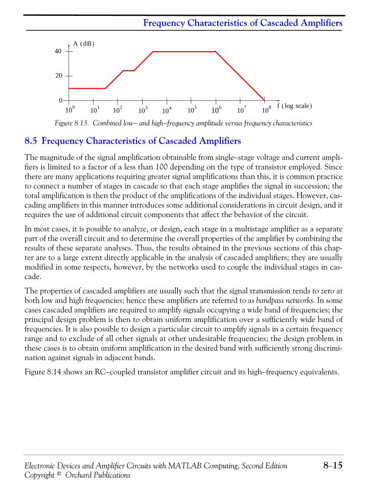
Electronic Devices and Amplifier Circuits with MATLAB Computing, Second Edition 8−15Copyright © Orchard Publications
Frequency Characteristics of Cascaded Amplifiers
Figure 8.13. Combined low− and high−frequency amplitude versus frequency characteristics
8.5 Frequency Characteristics of Cascaded Amplifiers
The magnitude of the signal amplification obtainable from single−stage voltage and current ampli-fiers is limited to a factor of a less than 100 depending on the type of transistor employed. Sincethere are many applications requiring greater signal amplifications than this, it is common practiceto connect a number of stages in cascade so that each stage amplifies the signal in succession; thetotal amplification is then the product of the amplifications of the individual stages. However, cas-cading amplifiers in this manner introduces some additional considerations in circuit design, and itrequires the use of additional circuit components that affect the behavior of the circuit.
In most cases, it is possible to analyze, or design, each stage in a multistage amplifier as a separatepart of the overall circuit and to determine the overall properties of the amplifier by combining theresults of these separate analyses. Thus, the results obtained in the previous sections of this chap-ter are to a large extent directly applicable in the analysis of cascaded amplifiers; they are usuallymodified in some respects, however, by the networks used to couple the individual stages in cas-cade.
The properties of cascaded amplifiers are usually such that the signal transmission tends to zero atboth low and high frequencies; hence these amplifiers are referred to as bandpass networks. In somecases cascaded amplifiers are required to amplify signals occupying a wide band of frequencies; theprincipal design problem is then to obtain uniform amplification over a sufficiently wide band offrequencies. It is also possible to design a particular circuit to amplify signals in a certain frequencyrange and to exclude of all other signals at other undesirable frequencies; the design problem inthese cases is to obtain uniform amplification in the desired band with sufficiently strong discrimi-nation against signals in adjacent bands.
Figure 8.14 shows an RC−coupled transistor amplifier circuit and its high−frequency equivalents.
A dB( )40
f scalelog( )100
20
0101 102 103 104 105 106 107 108
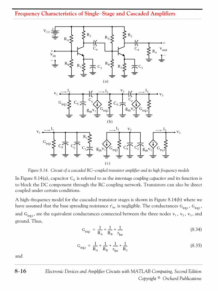
Frequency Characteristics of Single−Stage and Cascaded Amplifiers
8−16 Electronic Devices and Amplifier Circuits with MATLAB Computing, Second EditionCopyright © Orchard Publications
Figure 8.14. Circuit of a cascaded RC−coupled transistor amplifier and its high frequency models
In Figure 8.14(a), capacitor is referred to as the interstage coupling capacitor and its function isto block the DC component through the RC coupling network. Transistors can also be directcoupled under certain conditions.
A high−frequency model for the cascaded transistor stages is shown in Figure 8.14(b) where wehave assumed that the base spreading resistance is negligible. The conductances , ,
and , are the equivalent conductances connected between the three nodes , , , andground. Thus,
(8.34)
(8.35)
and
RA
RB
C4
R2
R3
VCC
a( )
b( )
c( )
I1
R1
gmv1
Cc
v1
CE
vin
vout
RA
RB
R2
R3 C3
C4 R4
C3
Geq1 CEGeq2
Cc
v2
gmv2 Geq3
v3I2 I3
Geq1
v1I1
CE Cc C1
I2
gmv1 Geq2CE C2 gmv2 Geq3
v2 v3I3
C4
r'be Geq1 Geq2
Geq3 v1 v2 v3
Geq11
RA------ 1
RB------ 1
rbe-------+ +=
Geq21
RA------ 1
RB------ 1
rbe------- 1
R2------+ + +=
Electronic Devices and Amplifier Circuits with MATLAB Computing, Second Edition 8−17Copyright © Orchard Publications
Frequency Characteristics of Cascaded Amplifiers
(8.36)
The model for the second stage of the amplifier has the same form as the model for a single−stageamplifier shown in Figure 8.9(c); hence the effect of the collector capacitance in this stage can beaccounted for by a Miller capacitance as shown in Figure 8.9(d). When this is done, the secondstage has the simplified representation shown in Figure 8.14(c). The Miller capacitance has thevalue
(8.37)where
(8.38)Similarly,
(8.39)
The model for the first stage of the amplifier differs from that of the second stage in that its loadhas a capacitive component as well as a resistive component; hence the Miller effect is slightly dif-ferent in the first stage. The first stage is as shown in Figure 8.14(c) where is the shunt capaci-tance that is present in the load of the first stage transistor, and the resistor is negligible incomparison to the reactance of capacitor . Typically, is one kilohm or less.
The value of depends on the mid−band value of the gain as defined in (8.39), the collectorcapacitance , and the half−power frequency for the output circuit of the first stage defined as
(8.40)
In terms of relations (8.39) and (8.40), the values of and can be found from
(8.41)
and(8.42)
We can also express in terms of using (8.42), that is,
(8.43)
If the resistance in the circuit of Figure 8.24(c) were negligible in comparison with the reac-tance of , then the simplified representation for the first stage would reduce to the same form asthat for the second stage, and the process could be repeated for each stage in a cascade of anynumber of stages. However, relation (8.43) shows that at , where is thehalf−power frequency for the output circuit of the first stage. Thus, it is convenient to neglect at frequencies up to . If is not neglected, and if the amplifier of Figure 8.24(c) is preceded by
Geq31
R2------ 1
R4------+=
C2 1 A2+( )CC=
A2 v3 v2⁄=
A1 v2 v1⁄=
C1
R1
C1 R1
R1 A1
Cc
ω2Geq2
CE C2 CC+ +--------------------------------=
R1 C1
R11
ω2A1CC-------------------- CE C2 CC+ +
gmCC--------------------------------= =
C1 A1CC=
R1 C1
R11
ω2C1------------=
R1
C1
ω ω2= R1 1 ω2C1⁄= ω2
R1
ω2 R1

Frequency Characteristics of Single−Stage and Cascaded Amplifiers
8−18 Electronic Devices and Amplifier Circuits with MATLAB Computing, Second EditionCopyright © Orchard Publications
yet another transistor stage, the Miller effect in this stage has a still more complicated form. Ofcourse, the Miller effect computations become more and more complicated as more stages arecascaded. To avoid these complications, it is practical to neglect and consider all computa-tions as approximations. Then with these approximations, the representation for each stage inthe cascade takes a simple form, and stage−by−stage analysis is easy.
From Figure 8.14(c),(8.44)
(8.45)
and division of (8.44) by (8.45) yields
(8.46)
Also, from Figure 8.14(c),(8.47)
and neglecting ,(8.48)
division of (8.47) by (8.48) yields
(8.49)
Example 8.5
For the cascaded amplifier circuit of Figure 8.15, the transistors are identical with ,, , , and . The quiescent collector cur-
rent in each stage is , and at this operating point , , ,, and the output resistance is very large and it can be neglected. Compute the
overall current gain at medium and high frequencies. Sketch and dimension the asymptotesfor the high−frequency amplitude characteristics.
Solution:
From Chapter 3, relation (3.78),
From relation (3.83),
R1
I3 gmv2–=
I2 Geq2 jω CE C2+( )+[ ]v2=
Ac2I3
I2----
gm–
Geq2 jω CE C2+( )+------------------------------------------------
gmGeq2
-----------–1
1 jω CE C2+( ) Geq2⁄+-------------------------------------------------------⋅= = =
I2 gmv1–=
R1I1 Geq1 jω CE Cc C1+ +( )+[ ]v1=
Ac1I2
I1----
gm–
Geq1 jω CE Cc C1+ +( )+------------------------------------------------------------
gmGeq1
-----------–1
1 jω CE Cc C1+ +( ) Geq1⁄+-------------------------------------------------------------------⋅= = =
RA 15 KΩ=
RB 3.3 KΩ= R2 2.6 KΩ= R3 0.68 KΩ= R4 0.5 KΩ=
IC 4 mA= β 100= r'b 50 Ω= CC 4 pF=
fT 100 MHz= ro
Ac
gm 40IC 40 4 10 3–×× 0.16 Ω 1–= = =
rbeβ
gm------- 100
0.16---------- 625 Ω= = =

Electronic Devices and Amplifier Circuits with MATLAB Computing, Second Edition 8−19Copyright © Orchard Publications
Frequency Characteristics of Cascaded Amplifiers
Figure 8.15. Cascaded amplifier for Example 8.5and from (3.93),
For the second stage of the amplifier, from (8.36),
From (8.27)
and since , the current gain of the second stage amplifier at medium frequencies is
From (8.37) the Miller effect capacitance is
From (8.35),
From (8.46),
and expressing in megaradians per second, we find that
RA
RB
C4R2
R3
VCC
vin
vout
RA
RB
R2
R3 C3
C4
R4
C3
CEgmωT------- 0.16
2π 108×--------------------- 255 pF= = =
Geq31
R2------ 1
R4------+ 1
2.6 KΩ------------------- 1
0.5 KΩ-------------------+ 2.4 mΩ 1–= = =
Amro
ro R2+-----------------gmReq=
ro R2»
Am2 gmReq
gmGeq3
----------- 0.162.4 10 3–×------------------------ 67= = = =
C2 1 Am2+( )CC 1 67+( )4 272 pF= = =
Geq21
RA------ 1
RB------ 1
rbe------- 1
R2------+ + + 1
15 KΩ----------------- 1
3.3 KΩ------------------- 1
50 Ω------------ 1
2.6 KΩ-------------------+ + + 2.4 mΩ 1–= = =
Ac2I3
I2----
gmGeq2
-----------–1
1 jω CE C2+( ) Geq2⁄+-------------------------------------------------------⋅= =
0.162.4 10 3–×------------------------–
11 jω 255 272+( ) 10 12–× 2.4 10 3–×⁄+-------------------------------------------------------------------------------------------⋅ 67–
11 jω2.2 10 7–×+---------------------------------------==
ω
Ac2 67–1
1 jω 4.5⁄+---------------------------=
Frequency Characteristics of Single−Stage and Cascaded Amplifiers
8−20 Electronic Devices and Amplifier Circuits with MATLAB Computing, Second EditionCopyright © Orchard Publications
With the frequency expressed in , we obtain
For the first stage of the amplifier we found above that
From (8.29)
and since , the current gain of the first stage amplifier at medium frequencies is
From (8.37) the Miller effect capacitance is
From (8.34),
From (8.49),
and expressing in megaradians per second, we find that
With the frequency expressed in , we obtain
The overall current gain is obtained by multiplying by . Thus,
MHz
Ac2 67–1
1 jf 0.72⁄+---------------------------=
Geq2 2.4 mΩ 1–=
Amro
ro R2+-----------------gmReq=
ro R2»
Am1 gmReqgm
Geq2
----------- 0.162.4 10 3–×------------------------ 67= = = =
C1 1 Am1+( )CC 1 67+( )4 272 pF= = =
Geq11
RA------ 1
RB------ 1
rbe-------+ + 1
15 KΩ----------------- 1
3.3 KΩ------------------- 1
625 Ω---------------+ + 2 mΩ 1–= = =
Ac1I2
I1----
gmGeq1
-----------–1
1 jω CE Cc C1+ +( ) Geq1⁄+-------------------------------------------------------------------⋅= =
0.162 10 3–×-------------------–
11 jω 255 4 272+ +( ) 10 12–× 2 10 3–×⁄+------------------------------------------------------------------------------------------------⋅ 80–
11 jω2.66 10 7–×+------------------------------------------==
ω
Ac1 80–1
1 jω 3.8⁄+---------------------------=
MHz
Ac1 80–1
1 jf 0.60⁄+---------------------------=
Ac Ac1 Ac2
Ac Ac1Ac2 80–1
1 jf 0.60⁄+---------------------------⎝ ⎠
⎛ ⎞ 67–1
1 jf 0.72⁄+---------------------------⎝ ⎠
⎛ ⎞ 5360 11 jf 0.60⁄+--------------------------- 1
1 jf 0.72⁄+---------------------------⋅ ⋅= = =
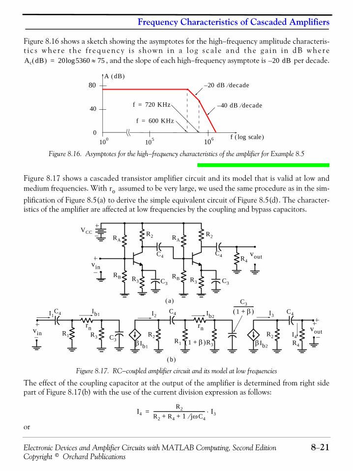
Electronic Devices and Amplifier Circuits with MATLAB Computing, Second Edition 8−21Copyright © Orchard Publications
Frequency Characteristics of Cascaded Amplifiers
Figure 8.16 shows a sketch showing the asymptotes for the high−frequency amplitude characteris-t i c s w h e r e t h e f r e q u e n c y i s s h o w n i n a l o g s c a l e a n d t h e g a i n i n d B w h e r e
, and the slope of each high−frequency asymptote is per decade.
Figure 8.16. Asymptotes for the high−frequency characteristics of the amplifier for Example 8.5
Figure 8.17 shows a cascaded transistor amplifier circuit and its model that is valid at low andmedium frequencies. With assumed to be very large, we used the same procedure as in the sim-plification of Figure 8.5(a) to derive the simple equivalent circuit of Figure 8.5(d). The character-istics of the amplifier are affected at low frequencies by the coupling and bypass capacitors.
Figure 8.17. RC−coupled amplifier circuit and its model at low frequencies
The effect of the coupling capacitor at the output of the amplifier is determined from right sidepart of Figure 8.17(b) with the use of the current division expression as follows:
or
Ac dB( ) 20 5360log 75≈= 20 dB–
A dB( )80
f scalelog( )100
40
0105 106
f 600 KHz=
f 720 KHz=
20– dB decade⁄
40– dB decade⁄
ro
RA
RB
C4
R2
R3
VCC
vin
vout
RA
RB
R2
R3 C3
C4 R4
C3
I1Ib1 I2 Ib2 I3
I4βIb1
βIb2
C4
R1
rn rnR3 C3
C4
R2R1 1 β+( )R3
C3
1 β+( )-----------------
R2
C4
vin
R4
vout
a( )
b( )
I4R2
R2 R4 1 jωC4⁄+ +------------------------------------------- I3⋅=

Frequency Characteristics of Single−Stage and Cascaded Amplifiers
8−22 Electronic Devices and Amplifier Circuits with MATLAB Computing, Second EditionCopyright © Orchard Publications
(8.50)
Defining the frequency as(8.51)
we express (8.50) as(8.52)
To simplify the procedure of deriving an expression for the gain we make use of the factthat the value required for the bypass capacitor is much larger than the value required for thecoupling capacitor . Thus, we choose the capacitors so that the low−frequency half−powerpoint is determined by , and with this choice acts as a short circuit while is making thetransition from a short circuit to an open circuit, and with this transition, the interstage networkhas the same form as the amplifier shown in Figure 8.5(d), and the current gain for each stage hasthe same form as (8.16). Thus, with acting as a short circuit we find that
* (8.53)
where(8.54)
and(8.55)
(8.56)
where, with acting as a short circuit, is the parallel combination of and in Figure8.17(b). Thus,
(8.57)
At very low frequencies acts as an open circuit and the interstage coupling capacitor con-tributes the factor
(8.58)
* The minus (−) sign stems from the fact that the current in Figure 8.17(b) has a direction opposite to the cur-rent in Figure 8.5(d).
I4
I3---- R2
R2 R4 1 jωC4⁄+ +-------------------------------------------
R2
R2 R4+----------------- jωC4 R2 R4+( )
1 jωC4 R2 R4+( )+--------------------------------------------⋅= =
ω4
ω41
C4 R2 R4+( )----------------------------=
I4
I3----
R2
R2 R4+----------------- jω ω4⁄
1 jω ω4⁄+-------------------------⋅=
I3 I2⁄
C3
C4
C3 C4 C3
C4
ACAm
1 k3+-------------- 1 jω ω3⁄+
1 jω 1 k3+( )ω3⁄+---------------------------------------------⋅–=
I3
I2
ω3 1 R3C3⁄=
AmβR'1
R1 rn+-----------------=
k31 β+( )R3
R'1 rn+------------------------=
C4 R'1 R1 R2
R'1R1R2
R1 R2+------------------=
C3 C4
jω ω5⁄1 jω ω5⁄+-------------------------

Electronic Devices and Amplifier Circuits with MATLAB Computing, Second Edition 8−23Copyright © Orchard Publications
Frequency Characteristics of Cascaded Amplifiers
where (8.59)
and is the equivalent resistance when acts as a short circuit and as an open circuit.Thus,
(8.60)
Usually, is much larger than the other resistors in that group, and thus
(8.61)
and with the factor contributed by the interstage coupling capacitor , the complete expressionfor the current gain is
(8.62)
Normally, the design process begins with the selection of the proper resistor values to establish asuitable quiescent point. Then, is chosen to make the break at occur at a desiredpoint below the band of the high frequencies of the signal. Finally, is chosen to make the breakat occur at some frequency below where acts as an open circuit.
Example 8.6 A cascaded transistor amplifier circuit and its model that is valid at low and medium frequenciesare shown in Figure 8.18.
The transistors are identical with , , , ,and . The quiescent collector current in each stage is , and the transistorparameters are , , , , and the output resistance is
very large in comparison with and thus it can be neglected. The coupling and bypass capacitorsare to be chosen to yield suitable performance at low frequencies.
a. Find the values of the resistances in the simplified low−frequency model in Figure 8.28(b).
b. The break frequency associated with the coupling capacitor at the output of the amplifier isto occur at . Compute the value of required in the output circuit.
c. The highest break frequency associated with the interstage coupling network is to be. Find , and, treating in the interstage network as a short circuit, find
the required value for the bypass capacitor .
ω51
ReqC4---------------=
Req C4 C3
Req R1 R2|| rn 1 β+( )R3+ +=
1 β+( )R3
ω51
R1 R2+( )C4------------------------------≈
C4
AC
Am1 k3+-------------- 1 jω ω3⁄+
1 jω 1 k3+( )ω3⁄+--------------------------------------------- jω ω5⁄
1 jω ω5⁄+-------------------------⋅ ⋅–=
C3 1 k3+( )ω3
C4
ω5 ω3 C3
RA 56 KΩ= RB 12 KΩ= R2 6.8 KΩ= R3 2.2 KΩ=
R4 1 KΩ= IC 1 mA=
β 200= r'b 200 Ω= CC 20 pF= fT 8 MHz= ro
R2
C4
16 Hz C4
1 k3+( )f3 160 Hz= ω3 C4
C3

Frequency Characteristics of Single−Stage and Cascaded Amplifiers
8−24 Electronic Devices and Amplifier Circuits with MATLAB Computing, Second EditionCopyright © Orchard Publications
Figure 8.18. Cascaded amplifier circuit and its low−frequency equivalent for Example 8.6.
d. The break frequency associated with the coupling capacitor in the interstage network,denoted as in relation (8.87), is to be at least as small as . Treating as an open cir-cuit, find the minimum value for in the interstage network.
Solution:
a. The values of , , and are given. Also,
From Chapter 3, relation (3.78),
From relation (3.83),
and from (3.79),
b. From relation (8.51),
RA
RB
C4R2
R3
VCC
vin
vout
RA
RB
R2
R3 C3
C4
R4
C3
I1Ib1 I2 Ib2 I3
I4
βIb1 βIb2
C4
R1
rn rn
R3 C3
C4
R2R1 1 β+( )R3
C3
1 β+( )-----------------
R2
C4
vinR4
vout
a( )
b( )
C4
ω5 ω3 C3
C4
R2 6.8 KΩ= R3 2.2 KΩ= R4 1 KΩ=
R1RARB
RA RA+-------------------- 56 12×
56 12+------------------ 9.9 KΩ= = =
1 β+( )R3 1 200+( )2.2 442 KΩ= =
gm 40IC 40 1 10 3–×× 40 mΩ 1–= = =
rbeβ
gm------- 200
40 10 3–×---------------------- 5 KΩ= = =
rn r'b rbe+ 200 Ω 5 KΩ+ 5.2 KΩ= = =
C41
R2 R4+( )ω4----------------------------- 1
6.8 1+( ) 103 2π 16×××------------------------------------------------------------- 1.28μF= = =

Electronic Devices and Amplifier Circuits with MATLAB Computing, Second Edition 8−25Copyright © Orchard Publications
Frequency Characteristics of Cascaded Amplifiers
c. From relation (8.57),
and from (8.56),
We are given that . Then,
or
and from (8.54),
d. With and with (8.61),
The computations for all examples and the end−of−chapter exercises, can be greatly simplified bywriting a MATLAB script such as that shown below and plot the overall current gain.
w=1:10:10^5; RA=56000; RB=12000; R2=6800; R3=2200; R4=1000;...beta=200; rbprime=200; Ic=10^(−3); f4=16; w4=2*pi*f4;...R1=RA*RB/(RA+RB); R1prime=R1*R2/(R1+R2); gm=40*Ic; rbe=beta/gm;...rn=rbprime+rbe; k3=(1+beta)*R3/(R1prime+rn); f3=160/(1+k3);...w3=2*pi*f3; C3=1/(w3*R3); w5=w3; C4b=1/((R2+R4)*w4);...C4d=1/((R1+R2)*w5); Am=beta*R1prime/(rn+R1prime);...Acnum=(Am.*(1+j.*w./w3).*(j.*w./w5));...Acden=(1+k3).*(1+j.*w./((1+k3).*w3)).*(1+j.*w./w5);...Ac=Acnum./Acden; AcdB=20.*log10(abs(Ac));...fprintf(' \n'); fprintf('RA = %2.2f K \t',RA/1000); fprintf(' \n');...fprintf('RB = %2.2f K \t',RB/1000); fprintf(' \n');...fprintf('R2 = %2.2f K \t',R2/1000); fprintf(' \n');...fprintf('R3 = %2.2f K \t',R3/1000); fprintf(' \n');fprintf('R4 = %2.2f K \t',R4/1000); fprintf(' \n');...fprintf('R1 = %2.2f K \t',R1/1000); fprintf(' \n');...fprintf('R1prime = %2.2f K \t',R1prime/1000); fprintf(' \n');...fprintf('rbprime = %2.2f K \t',rbprime/1000); fprintf(' \n');...fprintf('rbe = %2.2f K \t',rbe/1000); fprintf(' \n');...fprintf('rn = %2.2f K \t',rn/1000); fprintf(' \n');...fprintf('Ic = %2.2f mA \t',Ic*1000); fprintf(' \n');...
R'1R1R2
R1 R2+------------------ 9.9 6.8×
9.9 6.8+--------------------- 4.0 KΩ= = =
k31 β+( )R3
R'1 rn+------------------------ 1 200+( ) 2.2×
4.0 5.2+------------------------------------- 48.1= = =
1 k3+( )f3 160 Hz=
f316048.1---------- 3.33 Hz= =
ω3 2πf3 2π 3.33× 21 rad/s= = =
C31
ω3R3------------ 1
21 2.2 103××---------------------------------- 21.6 μF= = =
ω5 ω3 21 rad/s= =
C41
R1 R2+( )ω5------------------------------ 1
9.9 6.8+( ) 103× 21×----------------------------------------------------- 2.85 μF= = =

Frequency Characteristics of Single−Stage and Cascaded Amplifiers
8−26 Electronic Devices and Amplifier Circuits with MATLAB Computing, Second EditionCopyright © Orchard Publications
fprintf('beta = %2.0f \t',beta); fprintf(' \n');...fprintf('f4 = %2.2f Hz \t',f4); fprintf(' \n');...fprintf('w4 = %2.2f rps \t',w4); fprintf(' \n');...fprintf('C4b = %2.2f microF \t',C4b*10^6); fprintf(' \n');...fprintf('gm = %2.2f mmho \t',gm*1000); fprintf(' \n');...fprintf('k3 = %2.2f \t',k3); fprintf(' \n');...fprintf('f3 = %2.2f Hz \t',f3); fprintf(' \n');...fprintf('w3 = %2.2f rps \t',w3); fprintf(' \n');...fprintf('C3 = %2.2f microF \t',C3*10^6); fprintf(' \n');...fprintf('w5 = %2.2f rps \t',w5); fprintf(' \n');...fprintf('C4d = %2.2f microF \t',C4d*10^6); fprintf(' \n');...fprintf('Am = %2.2f \t',Am); fprintf(' \n');...f=w./(2.*pi); semilogx(f, AcdB); grid;...xlabel('Frequency in Hz (log scale)'); ylabel('Current gain (dB scale)');...title('Low−frequency characteristics for multistage amplifier, Example 8.8')
RA = 56.00 K RB = 12.00 K R2 = 6.80 K R3 = 2.20 K R4 = 1.00 K R1 = 9.88 K R1prime = 4.03 K rbprime = 0.20 K rbe = 5.00 K rn = 5.20 K Ic = 1.00 mA beta = 200 f4 = 16.00 Hz w4 = 100.53 rps C4b = 1.28 microF gm = 40.00 mmho k3 = 47.92 f3 = 3.27 Hz w3 = 20.55 rps C3 = 22.12 microF w5 = 20.55 rps C4d = 2.92 microF Am = 87.30
The plot for the current gain (in dB scale) versus frequency (in log scale) is shown in Figure 8.19.
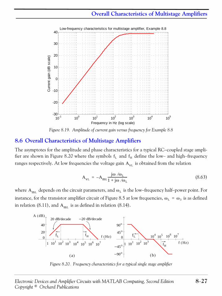
Electronic Devices and Amplifier Circuits with MATLAB Computing, Second Edition 8−27Copyright © Orchard Publications
Overall Characteristics of Multistage Amplifiers
Figure 8.19. Amplitude of current gain versus frequency for Example 8.8
8.6 Overall Characteristics of Multistage AmplifiersThe asymptotes for the amplitude and phase characteristics for a typical RC−coupled stage ampli-fier are shown in Figure 8.20 where the symbols and define the low− and high−frequencyranges respectively. At low frequencies the voltage gain is obtained from the relation
(8.63)
where depends on the circuit parameters, and is the low−frequency half−power point. For
instance, for the transistor amplifier circuit of Figure 8.5 at low frequencies, is as definedin relation (8.11), and is as defined in relation (8.14).
Figure 8.20. Frequency characteristics for a typical single stage amplifier
10-1
100
101
102
103
104
105
-30
-20
-10
0
10
20
30
40
Frequency in Hz (log scale)
Cur
rent
gai
n (d
B s
cale
)
Low-frequency characteristics for multistage amplifier, Example 8.8
fL fH
AvL
AvL AmL–jω ωL⁄
1 jω ωL⁄+--------------------------=
AmL ωL
ωL ω3=
AmL
101 102 103 104 105 106 107
f Hz( )20
40
1
fL
A dB( )
0
101 102 103
104 105 106 107
f Hz( )0
20 dB/decade
fH fL
20 dB/decade–
fH
45°
90°
90°–
45°–1
a( ) b( )

Frequency Characteristics of Single−Stage and Cascaded Amplifiers
8−28 Electronic Devices and Amplifier Circuits with MATLAB Computing, Second EditionCopyright © Orchard Publications
At high frequencies the voltage gain is obtained from the relation
(8.64)
where depends on the circuit parameters, and is the high−frequency half−power point.For instance, for the transistor amplifier circuit of Figure 8.9 at high frequencies, is asdefined in relation (8.28), and is as defined in relation (8.27).
We can obtain the combined low− and high−frequency characteristics for the voltage gain bymultiplying relation (8.89) by (8.90); thus,
(8.65)
If two identical stages such as that shown in Figure 8.18, are connected in cascade, the overallvoltage gain is obtained from the relation
(8.66)
The overall amplitude characteristics for two identical stages in cascade is shown in Figure 8.21.
Figure 8.21. Typical overall amplitude characteristics for two identical stages in cascade
By comparing the amplitude characteristics of Figures 8.20 and 8.21, we observe that the band-width between the half−power points decreases as more stages are connected in cascade. It canbe shown* that the half−power bandwidth of the cascade of identical stages is given by
(8.67)
where and is the half−power frequency for on stage amplifier at medium and high
frequencies. The quantity is referred to as the bandwidth reduction factor for identicalstages in cascade. For two stages the bandwidth reduction factor is , for three stages is ,and for four stages it is .
* The proof is left as an exercise for the reader at the end of this chapter.
AvH
AvH AmH–1
1 jω ωH⁄+--------------------------=
AmH ωH
ωH ω1=
AmH
Av
Av AmLAmHjω ωL⁄
1 jω ωL⁄+( ) 1 jω ωH⁄+( )--------------------------------------------------------------=
Av
Av Am2 jω ωL⁄( )2
1 jω ωL⁄+( )2 1 jω ωH⁄+( )2-------------------------------------------------------------------=
fL fH
f Hz( )020
40
A dB( ) 40 dB/decade 40 dB/decade–
n
Bn B1 21 n⁄ 1–=
B1 ωH= ωH
21 n⁄ 1– n0.64 0.51
0.43
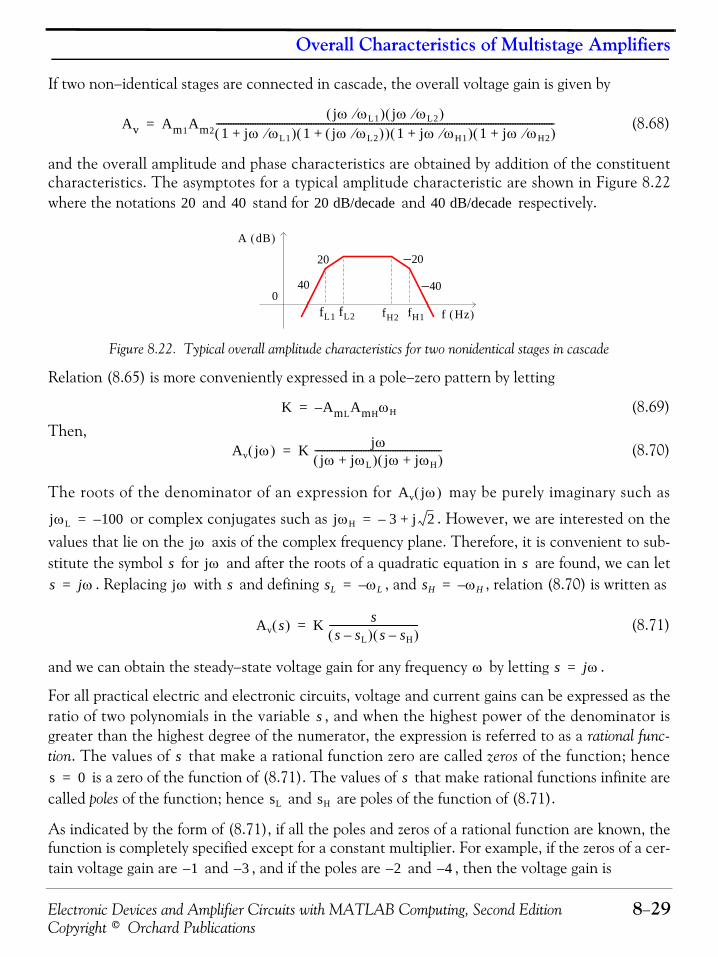
Electronic Devices and Amplifier Circuits with MATLAB Computing, Second Edition 8−29Copyright © Orchard Publications
Overall Characteristics of Multistage Amplifiers
If two non−identical stages are connected in cascade, the overall voltage gain is given by
(8.68)
and the overall amplitude and phase characteristics are obtained by addition of the constituentcharacteristics. The asymptotes for a typical amplitude characteristic are shown in Figure 8.22where the notations and stand for and respectively.
Figure 8.22. Typical overall amplitude characteristics for two nonidentical stages in cascade
Relation (8.65) is more conveniently expressed in a pole−zero pattern by letting
(8.69)Then,
(8.70)
The roots of the denominator of an expression for may be purely imaginary such as
or complex conjugates such as . However, we are interested on thevalues that lie on the axis of the complex frequency plane. Therefore, it is convenient to sub-stitute the symbol for and after the roots of a quadratic equation in are found, we can let
. Replacing with and defining , and , relation (8.70) is written as
(8.71)
and we can obtain the steady−state voltage gain for any frequency by letting .
For all practical electric and electronic circuits, voltage and current gains can be expressed as theratio of two polynomials in the variable , and when the highest power of the denominator isgreater than the highest degree of the numerator, the expression is referred to as a rational func-tion. The values of that make a rational function zero are called zeros of the function; hence
is a zero of the function of (8.71). The values of that make rational functions infinite arecalled poles of the function; hence and are poles of the function of (8.71).
As indicated by the form of (8.71), if all the poles and zeros of a rational function are known, thefunction is completely specified except for a constant multiplier. For example, if the zeros of a cer-tain voltage gain are and , and if the poles are and , then the voltage gain is
Av Am1Am2jω ωL1⁄( ) jω ωL2⁄( )
1 jω ωL1⁄+( ) 1 jω ωL2⁄( )+( ) 1 jω ωH1⁄+( ) 1 jω ωH2⁄+( )-------------------------------------------------------------------------------------------------------------------------------------------=
20 40 20 dB/decade 40 dB/decade
40 40–
20 20–
fL1 fL2 f Hz( )0
fH2 fH1
A dB( )
K AmLAmHωH–=
Av jω( ) K jωjω jωL+( ) jω jωH+( )
----------------------------------------------------=
Av jω( )
jωL 100–= jωH 3– j 2+=
jωs jω s
s jω= jω s sL ωL–= sH ωH–=
Av s( ) K ss sL–( ) s sH–( )
------------------------------------=
ω s jω=
s
ss 0= s
sL sH
1– 3– 2– 4–
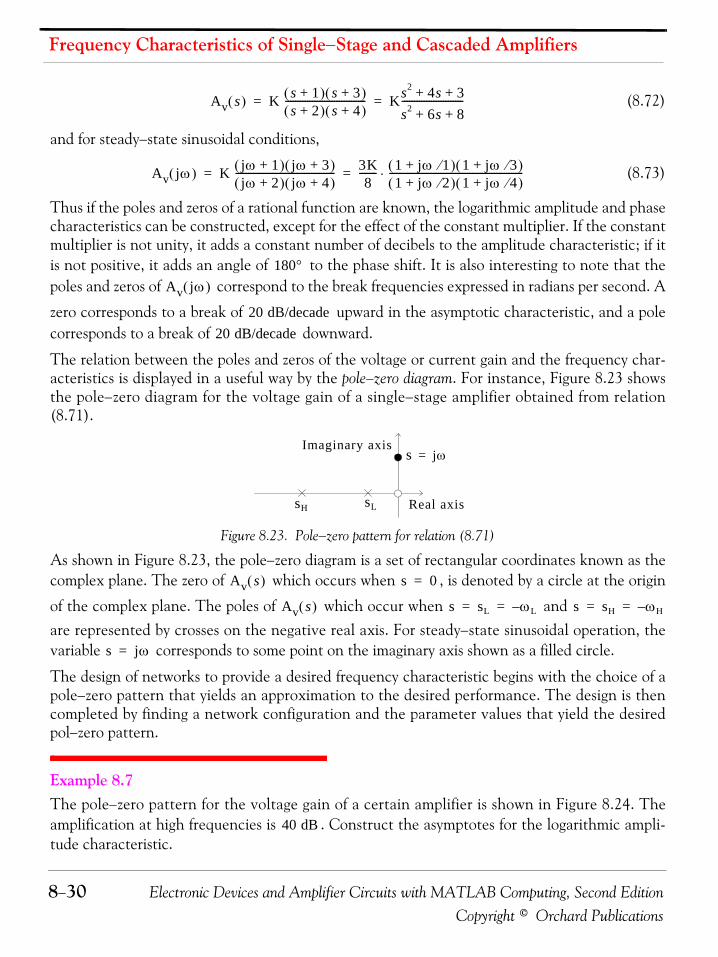
Frequency Characteristics of Single−Stage and Cascaded Amplifiers
8−30 Electronic Devices and Amplifier Circuits with MATLAB Computing, Second EditionCopyright © Orchard Publications
(8.72)
and for steady−state sinusoidal conditions,
(8.73)
Thus if the poles and zeros of a rational function are known, the logarithmic amplitude and phasecharacteristics can be constructed, except for the effect of the constant multiplier. If the constantmultiplier is not unity, it adds a constant number of decibels to the amplitude characteristic; if itis not positive, it adds an angle of to the phase shift. It is also interesting to note that thepoles and zeros of correspond to the break frequencies expressed in radians per second. A
zero corresponds to a break of upward in the asymptotic characteristic, and a polecorresponds to a break of downward.
The relation between the poles and zeros of the voltage or current gain and the frequency char-acteristics is displayed in a useful way by the pole−zero diagram. For instance, Figure 8.23 showsthe pole−zero diagram for the voltage gain of a single−stage amplifier obtained from relation(8.71).
Figure 8.23. Pole−zero pattern for relation (8.71)
As shown in Figure 8.23, the pole−zero diagram is a set of rectangular coordinates known as thecomplex plane. The zero of which occurs when , is denoted by a circle at the origin
of the complex plane. The poles of which occur when and are represented by crosses on the negative real axis. For steady−state sinusoidal operation, thevariable corresponds to some point on the imaginary axis shown as a filled circle.
The design of networks to provide a desired frequency characteristic begins with the choice of apole−zero pattern that yields an approximation to the desired performance. The design is thencompleted by finding a network configuration and the parameter values that yield the desiredpol−zero pattern.
Example 8.7 The pole−zero pattern for the voltage gain of a certain amplifier is shown in Figure 8.24. Theamplification at high frequencies is . Construct the asymptotes for the logarithmic ampli-tude characteristic.
Av s( ) K s 1+( ) s 3+( )s 2+( ) s 4+( )
--------------------------------- Ks2 4s 3+ +
s2 6s 8+ +-------------------------= =
Av jω( ) K jω 1+( ) jω 3+( )jω 2+( ) jω 4+( )
----------------------------------------- 3K8
------- 1 jω 1⁄+( ) 1 jω 3⁄+( )1 jω 2⁄+( ) 1 jω 4⁄+( )
-------------------------------------------------------⋅= =
180°Av jω( )
20 dB/decade20 dB/decade
s jω=Imaginary axis
Real axissH sL
Av s( ) s 0=
Av s( ) s sL ωL–= = s sH ωH–= =
s jω=
40 dB
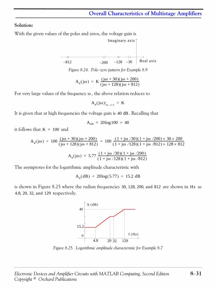
Electronic Devices and Amplifier Circuits with MATLAB Computing, Second Edition 8−31Copyright © Orchard Publications
Overall Characteristics of Multistage Amplifiers
Solution:
With the given values of the poles and zeros, the voltage gain is
Figure 8.24. Pole−zero pattern for Example 8.9
For very large values of the frequency , the above relation reduces to
It is given that at high frequencies the voltage gain is . Recalling that
it follows that and
The asymptotes for the logarithmic amplitude characteristic with
is shown in Figure 8.25 where the radian frequencies are shown in as respectively.
Figure 8.25. Logarithmic amplitude characteristic for Example 8.7
Imaginary axis
Real axis30–812– 128–200–
Av jω( ) K jω 30+( ) jω 200+( )jω 128+( ) jω 812+( )
-----------------------------------------------------=
ω
Av jω( ) ω ∞→ K=
40 dB
AdB 20 100log 40= =
K 100=
Av jω( ) 100 jω 30+( ) jω 200+( )jω 128+( ) jω 812+( )
----------------------------------------------------- 100 1 jω 30⁄+( ) 1 jω 200⁄+( ) 30 200××1 jω 128⁄+( ) 1 jω 812⁄+( ) 128 812××
-------------------------------------------------------------------------------------------------= =
Av jω( ) 5.77 1 jω 30⁄+( ) 1 jω 200⁄+( )1 jω 128⁄+( ) 1 jω 812⁄+( )
-------------------------------------------------------------------=
Av dB( ) 20 5.77( )log 15.2 dB= =
30 128 200 and 812, , , Hz4.8 20 32 and 129, , ,
A dB( )40
0 f Hz( )
15.2
4.8 20 32 129
Frequency Characteristics of Single−Stage and Cascaded Amplifiers
8−32 Electronic Devices and Amplifier Circuits with MATLAB Computing, Second EditionCopyright © Orchard Publications
8.7 Amplification and Power Gain in Three or More Cascaded AmplifiersTransistor amplifiers are conveniently characterized as current amplifiers. A typical transistorradio many employ a cascade of five amplifier stages. The first four are designed to yield thegreatest possible current amplification, and the fifth stage is a power amplifier designed to pro-duce the greatest possible power output. Let us consider the equivalent circuit of a voltage ampli-fier shown in Figure 8.26.
Figure 8.26. Equivalent circuit of a typical voltage amplifier
The instantaneous input power to this amplifier is
(8.74)
and the instantaneous output power is
(8.75)
The power gain in dB is defined as
(8.76)
Thus, the power gain of the circuit of Figure 8.26 is
(8.77)
In communications circuits it is desirable to make , and in this case the second term onthe right side of (8.77) is zero. Denoting the voltage gain as we obtain
(8.78)
Example 8.8 For the three−stage amplifier shown in Figure 8.27, find:
v1 v2 RL
i2i1
μv1
R2R1
pinv1
2
R1------=
poutv2
2
RL------=
Gp 10poutpin----------log=
Gp 10 v22 RL⁄
v12 R1⁄
---------------log 10 v22R1
v12RL
------------log 20 v2
v1-----log 10 R1
RL------log+= = =
RL R1=
Av
Av 20 v2
v1-----log=
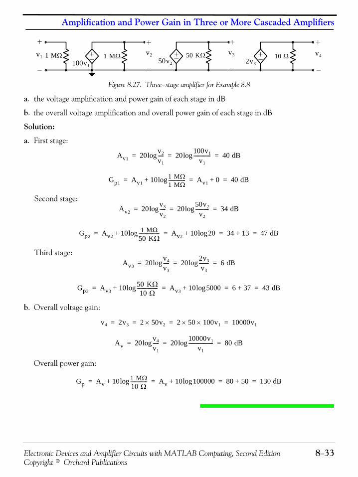
Electronic Devices and Amplifier Circuits with MATLAB Computing, Second Edition 8−33Copyright © Orchard Publications
Amplification and Power Gain in Three or More Cascaded Amplifiers
Figure 8.27. Three−stage amplifier for Example 8.8
a. the voltage amplification and power gain of each stage in dB
b. the overall voltage amplification and overall power gain of each stage in dB
Solution:
a. First stage:
Second stage:
Third stage:
b. Overall voltage gain:
Overall power gain:
v1100v1
50 KΩ50v2 2v3
1 MΩ1 MΩ 10 Ωv2 v3 v4
Av1 20 v2
v1-----log 20 100v1
v1--------------log 40 dB= = =
Gp1 Av1 10 1 MΩ1 MΩ--------------log+ Av1 0+ 40 dB= = =
Av2 20 v3
v2-----log 20 50v2
v2-----------log 34 dB= = =
Gp2 Av2 10 1 MΩ50 KΩ-----------------log+ Av2 10 20log+ 34 13+ 47 dB= = = =
Av3 20 v4
v3-----log 20 2v3
v3--------log 6 dB= = =
Gp3 Av3 10 50 KΩ10 Ω
-----------------log+ Av3 10 5000log+ 6 37+ 43 dB= = = =
v4 2v3 2 50v2× 2 50 100v1×× 10000v1= = = =
Av 20 v4
v1-----log 20 10000v1
v1--------------------log 80 dB= = =
Gp Av 10 1 MΩ10 Ω--------------log+ Av 10 100000log+ 80 50+ 130 dB= = = =
Frequency Characteristics of Single−Stage and Cascaded Amplifiers
8−34 Electronic Devices and Amplifier Circuits with MATLAB Computing, Second EditionCopyright © Orchard Publications
8.8 Summary• Periodic signals can be represented as the superposition of sinusoidal components by a Fourier
series of the form
where is the DC component of the composite signal, is the fundamental frequency or firstharmonic, , is the second harmonic, is the third harmonic, and so on.
• Signals that are not can be approximated by the superposition of a number of sinusoidal com-ponents expressed as
where is the DC component of the composite signal, and , , , and so on, are notharmonically related.
• The frequency spectrum of a signal reveals information about the frequencies and amplitude,but it contains no information about the phase angles of the components.
• Amplification decreases at high frequencies as a result of the parasitic capacitances in the cir-cuit, and decreases at low frequencies because of the presence of coupling capacitors.
• For a good designed amplifier, the amplification near the lower and near the higher band offrequencies should not be less than 70 percent of the amplification in the middle of the band.
• If an amplifier retards the phase of each sinusoidal component of the signal in direct propor-tion to the frequency of that component, then the waveform of the output signal is an exactcopy of the input waveform, but it is delayed in time.
• The behavior of transistor amplifier at low frequencies is affected by the action of the bypasscapacitor that is in parallel with the emitter resistor.
• Transistor amplifier circuits designed for low frequencies are discussed in Section 8.2.
• Transistor amplifier circuits designed for high frequencies are discussed in Section 8.3.
• The amplifying property of the transistor which increases the apparent value of the collectorcapacitance is known as the Miller effect.
• The frequency dependence of various amplifier circuits is examined by treating the low−fre-quency characteristics separately from the high−frequency characteristics. However, the com-bined low− and high−frequency characteristics can be displayed on a single set of coordinates.
• To achieve higher gains, we use multistage amplifier circuits. The overall characteristics ofmultistage amplifiers can be easily approximated and displayed with the use of asymptotes.
v t( ) V V1 ωt θ1+( )cos V2 2ωt θ2+( )cos V3 3ωt θ3+( ) …+cos+ + +=
V ω2ω 3ω
v t( ) V V1 ω1t θ1+( )cos V2 ω2t θ2+( )cos V3 ω3t θ3+( ) …+cos+ + +=
V ω1 ω2 ω3
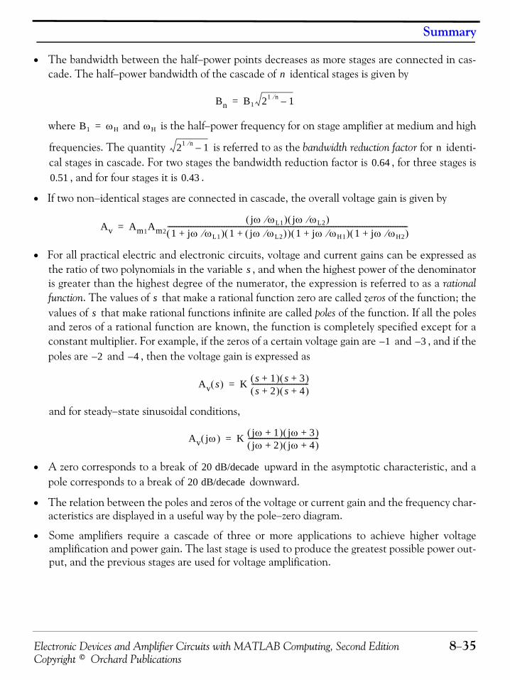
Electronic Devices and Amplifier Circuits with MATLAB Computing, Second Edition 8−35Copyright © Orchard Publications
Summary
• The bandwidth between the half−power points decreases as more stages are connected in cas-cade. The half−power bandwidth of the cascade of identical stages is given by
where and is the half−power frequency for on stage amplifier at medium and high
frequencies. The quantity is referred to as the bandwidth reduction factor for identi-cal stages in cascade. For two stages the bandwidth reduction factor is , for three stages is
, and for four stages it is .
• If two non−identical stages are connected in cascade, the overall voltage gain is given by
• For all practical electric and electronic circuits, voltage and current gains can be expressed asthe ratio of two polynomials in the variable , and when the highest power of the denominatoris greater than the highest degree of the numerator, the expression is referred to as a rationalfunction. The values of that make a rational function zero are called zeros of the function; thevalues of that make rational functions infinite are called poles of the function. If all the polesand zeros of a rational function are known, the function is completely specified except for aconstant multiplier. For example, if the zeros of a certain voltage gain are and , and if thepoles are and , then the voltage gain is expressed as
and for steady−state sinusoidal conditions,
• A zero corresponds to a break of upward in the asymptotic characteristic, and apole corresponds to a break of downward.
• The relation between the poles and zeros of the voltage or current gain and the frequency char-acteristics are displayed in a useful way by the pole−zero diagram.
• Some amplifiers require a cascade of three or more applications to achieve higher voltageamplification and power gain. The last stage is used to produce the greatest possible power out-put, and the previous stages are used for voltage amplification.
n
Bn B1 21 n⁄ 1–=
B1 ωH= ωH
21 n⁄ 1– n0.64
0.51 0.43
Av Am1Am2jω ωL1⁄( ) jω ωL2⁄( )
1 jω ωL1⁄+( ) 1 jω ωL2⁄( )+( ) 1 jω ωH1⁄+( ) 1 jω ωH2⁄+( )-------------------------------------------------------------------------------------------------------------------------------------------=
s
ss
1– 3–
2– 4–
Av s( ) K s 1+( ) s 3+( )s 2+( ) s 4+( )
---------------------------------=
Av jω( ) K jω 1+( ) jω 3+( )jω 2+( ) jω 4+( )
-----------------------------------------=
20 dB/decade20 dB/decade
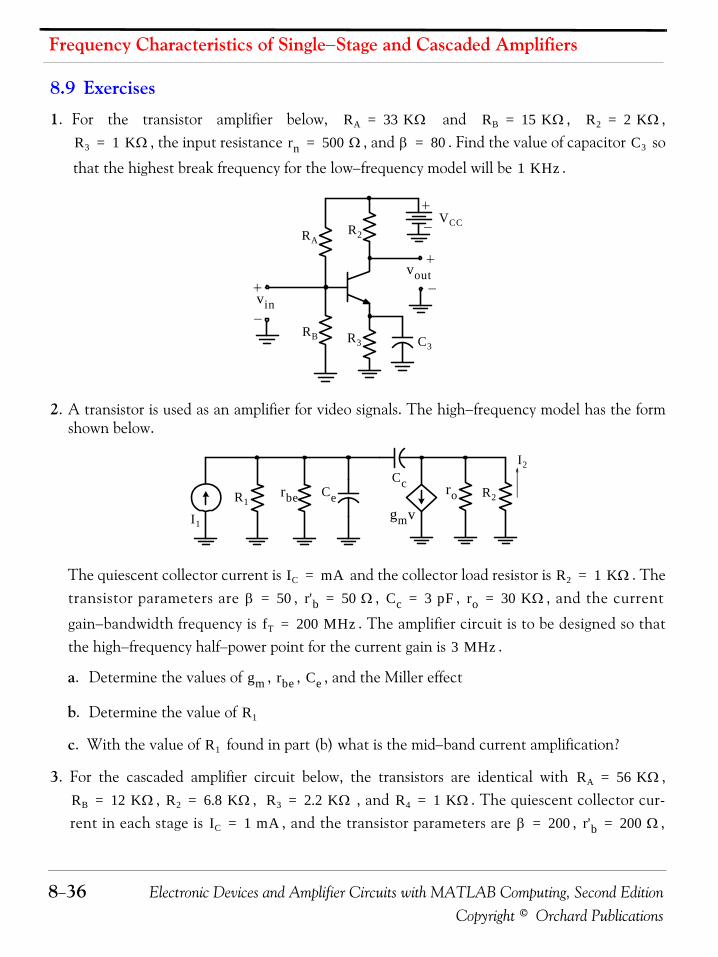
Frequency Characteristics of Single−Stage and Cascaded Amplifiers
8−36 Electronic Devices and Amplifier Circuits with MATLAB Computing, Second EditionCopyright © Orchard Publications
8.9 Exercises
1. For the transistor amplifier below, and , ,, the input resistance , and . Find the value of capacitor so
that the highest break frequency for the low−frequency model will be .
2. A transistor is used as an amplifier for video signals. The high−frequency model has the formshown below.
The quiescent collector current is and the collector load resistor is . Thetransistor parameters are , , , , and the current
gain−bandwidth frequency is . The amplifier circuit is to be designed so thatthe high−frequency half−power point for the current gain is .
a. Determine the values of , , , and the Miller effect
b. Determine the value of
c. With the value of found in part (b) what is the mid−band current amplification?
3. For the cascaded amplifier circuit below, the transistors are identical with ,, , , and . The quiescent collector cur-
rent in each stage is , and the transistor parameters are , ,
RA 33 KΩ= RB 15 KΩ= R2 2 KΩ=
R3 1 KΩ= rn 500 Ω= β 80= C3
1 KHz
R3RB
RA
C3
vin
VCCR2
vout
Cc
gmvR2
I2
CerbeR1
I1
ro
IC mA= R2 1 KΩ=
β 50= r'b 50 Ω= Cc 3 pF= ro 30 KΩ=
fT 200 MHz=
3 MHz
gm rbe Ce
R1
R1
RA 56 KΩ=
RB 12 KΩ= R2 6.8 KΩ= R3 2.2 KΩ= R4 1 KΩ=
IC 1 mA= β 200= r'b 200 Ω=

Electronic Devices and Amplifier Circuits with MATLAB Computing, Second Edition 8−37Copyright © Orchard Publications
Exercises
, , and the output resistance is very large in comparison with and thus it can be neglected.
a. Find the parameter values of the simplified high−frequency model circuit shown below.
b. Neglecting the effect of the resistance in the model circuit above, find the overall cur-rent gain .
c. Sketch and dimension the asymptotes for the high−frequency amplitude characteristics.
4. Prove that the half−power bandwidth of the cascade of identical stages is given by
where and is the half−power frequency for one stage amplifier at medium andhigh frequencies. Hint: Begin with the assumption that the amplitude of the voltage gain of aone−stage amplifier is given by
5. The pole−zero patterns for the voltage gain of two transistor amplifiers are shown below.
CC 20 pF= fT 8 MHz= ro R2
RA
RB
C4
R2
R3
VCC
vin
vout
RA
RB
R2
R3 C3
C4 R4
C3
R1Geq1
v1I1
CE CcC1
I2
gmv1 Geq2
CE C2
gmv2Geq3
v2 v3
I3
R1
Ac I3 I1⁄=
n
Bn B1 21 n⁄ 1–=
B1 ωH= ωH
Av A Am 1 ω ωH⁄( )2+( )⁄= =
Imaginary axis Imaginary axis
Real axis Real axisω1–10ω1– ω1–2ω1–20ω1–
a( ) b( )

Frequency Characteristics of Single−Stage and Cascaded Amplifiers
8−38 Electronic Devices and Amplifier Circuits with MATLAB Computing, Second EditionCopyright © Orchard Publications
a. Will both of these amplifiers transmit DC signals?
b. Use MATLAB to obtain the plot for the amplitude characteristic for the pole−zero patternof Figure (b) assuming that the function is multiplied by the constant .
6. A certain stereo amplifier delivers a sinusoidal voltage of on open circuit and hasan internal resistance of . This amplifier is to deliver a signal to a loudspeaker whoseresistance is .
a. If the amplifier is connected directly to the loudspeaker, how much power does it deliver tothe loudspeaker?
b. A cascade of amplifier stages similar to that shown in Figure (a) below is to be used toamplify the signal from the stereo amplifier and deliver to the loudspeaker. Two typesof amplifiers shown in Figures (b) and (c) below are available for the cascade connection.Which of these amplifiers can deliver to the loudspeaker with the smallest input volt-age?
c. Which of the amplifiers in Figures (b) and (c) yields the greatest no−load voltage amplifi-cation?
d. Draw the circuit diagram for a cascade of stages like those in Figures (b) and (c) that willmeet the specifications of part (b) above. Use the smallest possible number of stages andshow how a potentiometer can be used in the first stage as a volume control.
K 40 000,=
10 mV RMS500 Ω
10 Ω
10 w
10 w
1 MΩ
v1μv1
50 KΩ
μv2 μv3
RL
10 Ω
v2 v3
50v1v1 v1
a( )
b( ) c( )
1v1
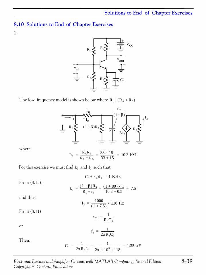
Electronic Devices and Amplifier Circuits with MATLAB Computing, Second Edition 8−39Copyright © Orchard Publications
Solutions to End−of−Chapter Exercises
8.10 Solutions to End−of−Chapter Exercises1.
The low−frequency model is shown below where
where
For this exercise we must find and such that
From (8.15),
and thus,
From (8.11)
or
Then,
R3RB
RA
C3
vin
VCCR2
vout
R1 RA RB+( )||
R2R1
I1 IB
rnI2
βIB
1 β+( )R3
C3
1 β+( )----------------
R1RARB
RA RB+------------------- 33 15 ×
33 15+-------------------- 10.3 KΩ= = =
k3 f3
1 k3+( )f3 1 KHz=
k31 β+( )R3
R1 rn+------------------------ 1 80+( ) 1×
10.3 0.5+----------------------------- 7.5= = =
f31000
1 7.5+( )--------------------- 118 Hz≈=
ω31
R3C3------------=
f31
2πR3C3-------------------=
C31
2πR3f3----------------- 1
2π 103× 118×------------------------------------ 1.35 μF= = =
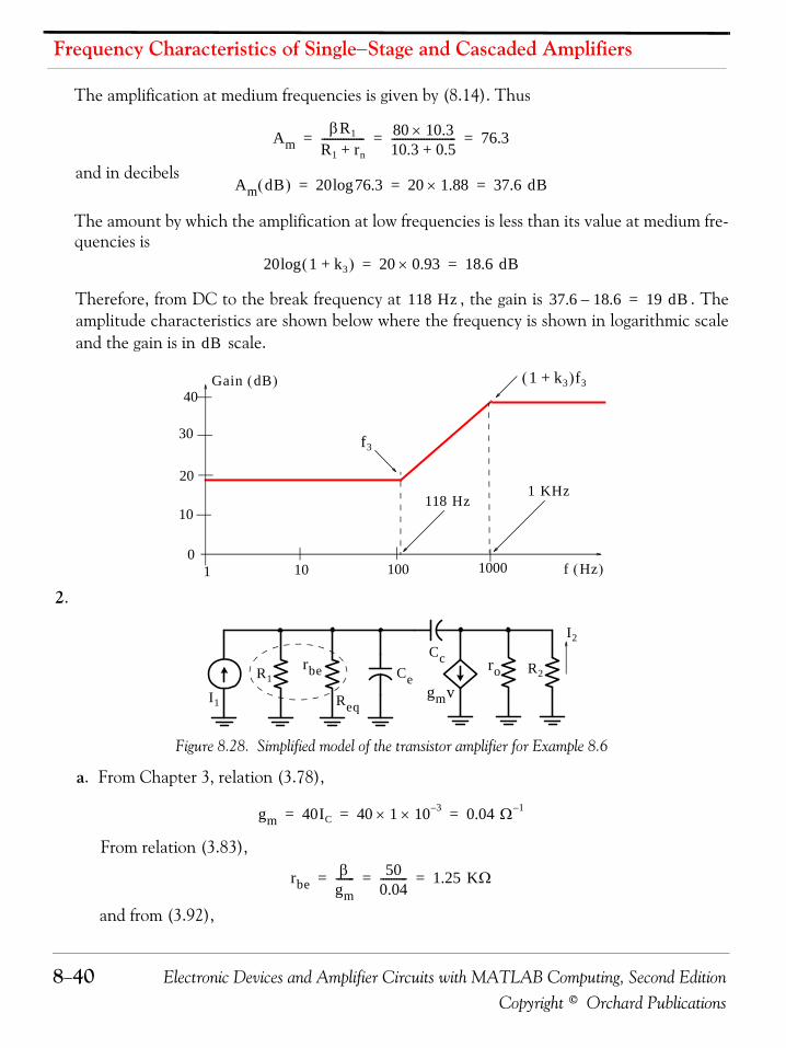
Frequency Characteristics of Single−Stage and Cascaded Amplifiers
8−40 Electronic Devices and Amplifier Circuits with MATLAB Computing, Second EditionCopyright © Orchard Publications
The amplification at medium frequencies is given by (8.14). Thus
and in decibels
The amount by which the amplification at low frequencies is less than its value at medium fre-quencies is
Therefore, from DC to the break frequency at , the gain is . Theamplitude characteristics are shown below where the frequency is shown in logarithmic scaleand the gain is in scale.
2.
Figure 8.28. Simplified model of the transistor amplifier for Example 8.6
a. From Chapter 3, relation (3.78),
From relation (3.83),
and from (3.92),
AmβR1
R1 rn+---------------- 80 10.3×
10.3 0.5+------------------------ 76.3= = =
Am dB( ) 20 76.3log 20 1.88× 37.6 dB= = =
20 1 k3+( )log 20 0.93× 18.6 dB= =
118 Hz 37.6 18.6– 19 dB=
dB
10
20
40
f Hz( )0
1 10 100 1000
Gain dB( )
118 Hz1 KHz
1 k3+( )f3
f330
Cc
gmvR2
I2
CerbeR1
I1
ro
Req
gm 40IC 40 1 10 3–×× 0.04 Ω 1–= = =
rbeβ
gm------- 50
0.04---------- 1.25 KΩ= = =
Electronic Devices and Amplifier Circuits with MATLAB Computing, Second Edition 8−41Copyright © Orchard Publications
Solutions to End−of−Chapter Exercises
This indicates that large current amplification is provided at frequencies up to .
From (3.93),
The Miller effect is where
Thus,
and this indicates that the dominant effect at high frequencies is the Miller effect.
b. From (8.19),
and by substitution into (8.33) with
c. The medium frequency current amplification is given by (8.27) as
fβfT
β---- 200
50--------- 4 MHz= = =
4 MHz
CegmωT------- 0.04
2π 2 108××------------------------------ 31.8 pF= = =
1 A+( )Cc
A gmR2≈ 0.04 1000× 40= =
1 A+( )Cc 41 3 10 12–×× 123 10 12–× 123 pF= = =
AgmroR2
ro R2+( )---------------------- 0.04 30 106××
31 103×------------------------------------- 38.7= = =
f1 3 MHz=
3 106× 4 106×1 1.25 103× R1⁄+
1 38.7 3 10 12–×× 31.8 10 12–×⁄+--------------------------------------------------------------------------------⋅=
4 1 1.25 103
R1--------×+⎝ ⎠
⎛ ⎞ 3 1 3.65+( ) 14= =
5 103×R1
----------------- 10=
R1 500 Ω=
Am
Amro
ro R2+-----------------gmReq
roro R2+-----------------gm
R1rbeR1 rbe+------------------- 30
31------ 0.04 500 1250×
1750--------------------------- 13.8=××= = =
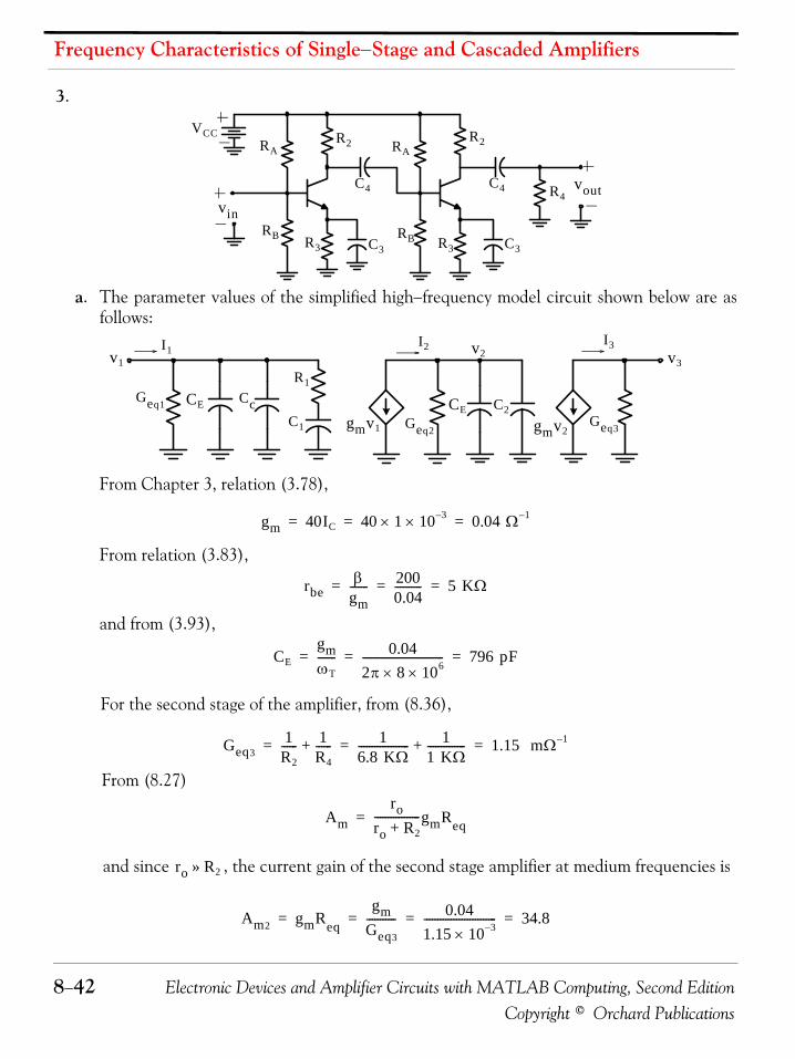
Frequency Characteristics of Single−Stage and Cascaded Amplifiers
8−42 Electronic Devices and Amplifier Circuits with MATLAB Computing, Second EditionCopyright © Orchard Publications
3.
a. The parameter values of the simplified high−frequency model circuit shown below are asfollows:
From Chapter 3, relation (3.78),
From relation (3.83),
and from (3.93),
For the second stage of the amplifier, from (8.36),
From (8.27)
and since , the current gain of the second stage amplifier at medium frequencies is
RA
RB
C4
R2
R3
VCC
vin
vout
RA
RB
R2
R3 C3
C4 R4
C3
R1Geq1
v1I1
CE CcC1
I2
gmv1 Geq2
CE C2
gmv2Geq3
v2 v3
I3
gm 40IC 40 1 10 3–×× 0.04 Ω 1–= = =
rbeβ
gm------- 200
0.04---------- 5 KΩ= = =
CEgmωT------- 0.04
2π 8 106××------------------------------ 796 pF= = =
Geq31
R2------ 1
R4------+ 1
6.8 KΩ------------------- 1
1 KΩ--------------+ 1.15 mΩ 1–= = =
Amro
ro R2+-----------------gmReq=
ro R2»
Am2 gmReqgm
Geq3
----------- 0.041.15 10 3–×--------------------------- 34.8= = = =

Electronic Devices and Amplifier Circuits with MATLAB Computing, Second Edition 8−43Copyright © Orchard Publications
Solutions to End−of−Chapter Exercises
From (8.37) the Miller effect capacitance is
From (8.35),
From (8.46),
and expressing in megaradians per second, we find that
With the frequency expressed in , we obtain
For the first stage of the amplifier we found above that
From (8.27)
and since , the current gain of the first stage amplifier at medium frequencies is
From (8.37) the Miller effect capacitance is
b. Neglecting , from (8.34),
From (8.49),
C2 1 Am2+( )CC 1 34.8+( )20 716 pF= = =
Geq21
RA------ 1
RB------ 1
rbe------ 1
R2------+ + + 1
56 KΩ----------------- 1
12 KΩ----------------- 1
5 KΩ-------------- 1
6.8 KΩ-------------------+ + + 0.45 mΩ 1–= = =
Ac2I3
I2----
gmGeq2
-----------–1
1 jω CE C2+( ) Geq2⁄+-------------------------------------------------------⋅= =
0.040.45 10 3–×---------------------------–
11 jω 796 716+( ) 10 12–× 0.45 10 3–×⁄+----------------------------------------------------------------------------------------------⋅ 89–
11 jω3.36 10 6–×+------------------------------------------==
ω
Ac2 89–1
1 jω 0.3⁄+---------------------------=
KHz
Ac2 67–1
1 jf 47.4⁄+---------------------------=
Geq2 0.45 mΩ 1–=
Amro
ro R2+-----------------gmReq=
ro R2»
Am1 gmReqgm
Geq2
----------- 0.040.45 10 3–×--------------------------- 89= = = =
C1 1 Am1+( )CC 1 89+( )20 1800 pF= = =
R1
Geq11
RA------ 1
RB------ 1
rbe-------+ + 1
56 KΩ----------------- 1
12 KΩ----------------- 1
5 KΩ--------------+ + 0.30 mΩ 1–= = =
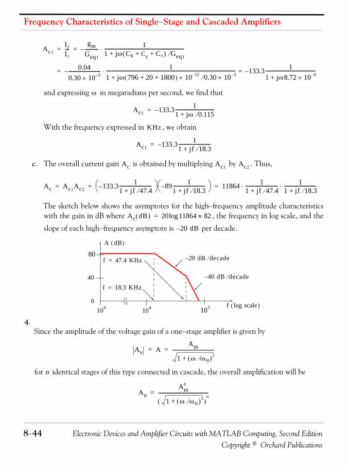
Frequency Characteristics of Single−Stage and Cascaded Amplifiers
8−44 Electronic Devices and Amplifier Circuits with MATLAB Computing, Second EditionCopyright © Orchard Publications
and expressing in megaradians per second, we find that
With the frequency expressed in , we obtain
c. The overall current gain is obtained by multiplying by . Thus,
The sketch below shows the asymptotes for the high−frequency amplitude characteristicswith the gain in dB where , the frequency in log scale, and the
slope of each high−frequency asymptote is per decade.
4.Since the amplitude of the voltage gain of a one−stage amplifier is given by
for identical stages of this type connected in cascade, the overall amplification will be
Ac1I2
I1----
gmGeq1
-----------–1
1 jω CE Cc C1+ +( ) Geq1⁄+-------------------------------------------------------------------⋅= =
0.040.30 10 3–×---------------------------–
11 jω 796 20 1800+ +( ) 10 12–× 0.30 10 3–×⁄+-------------------------------------------------------------------------------------------------------------⋅ 133.3–
11 jω8.72 10 6–×+------------------------------------------==
ω
Ac1 133.3–1
1 jω 0.115⁄+---------------------------------=
KHz
Ac1 133.3–1
1 jf 18.3⁄+---------------------------=
Ac Ac1 Ac2
Ac Ac1Ac2 133.3–1
1 jf 47.4⁄+---------------------------⎝ ⎠
⎛ ⎞ 89–1
1 jf 18.3⁄+---------------------------⎝ ⎠
⎛ ⎞ 11864 11 jf 47.4⁄+--------------------------- 1
1 jf 18.3⁄+---------------------------⋅ ⋅= = =
Ac dB( ) 20 11864log 82≈=
20 dB–
A dB( )
80
f scalelog( )100
40
0104 105
f 18.3 KHz=
f 47.4 KHz= 20– dB decade⁄
40– dB decade⁄
Av AAm
1 ω ωH⁄( )2+-----------------------------------= =
n
AnAm
n
1 ω ωH⁄( )2+( )n
------------------------------------------=
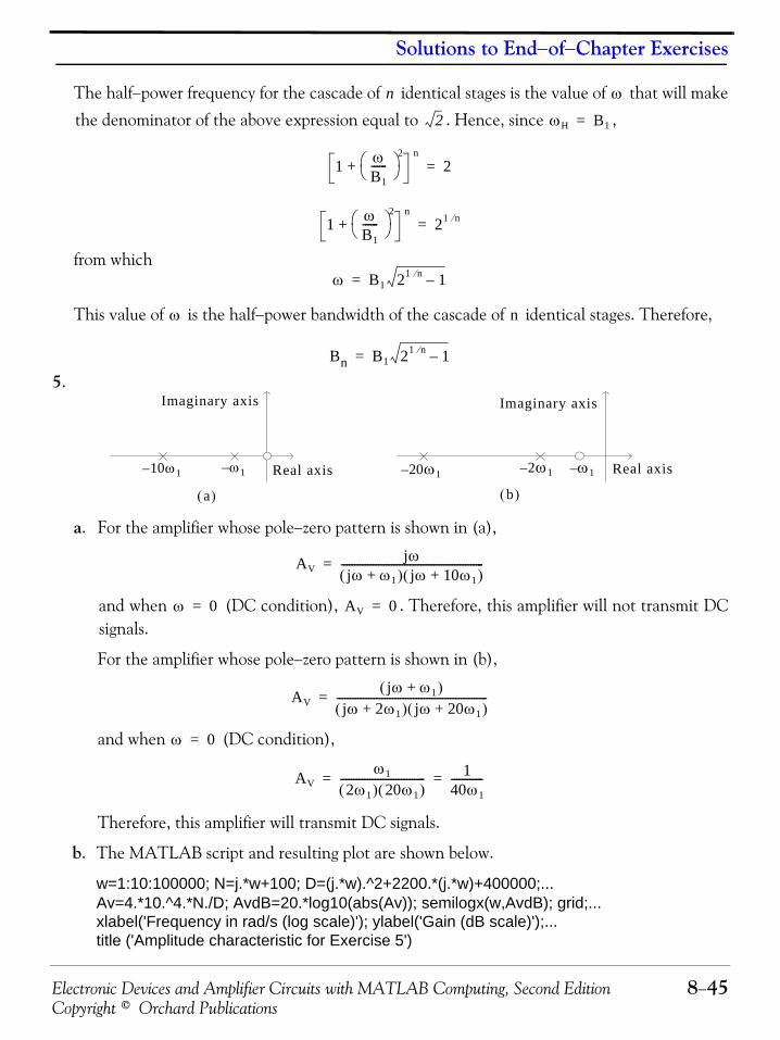
Electronic Devices and Amplifier Circuits with MATLAB Computing, Second Edition 8−45Copyright © Orchard Publications
Solutions to End−of−Chapter Exercises
The half−power frequency for the cascade of identical stages is the value of that will make
the denominator of the above expression equal to . Hence, since ,
from which
This value of is the half−power bandwidth of the cascade of identical stages. Therefore,
5.
a. For the amplifier whose pole−zero pattern is shown in (a),
and when (DC condition), . Therefore, this amplifier will not transmit DCsignals.
For the amplifier whose pole−zero pattern is shown in (b),
and when (DC condition),
Therefore, this amplifier will transmit DC signals.
b. The MATLAB script and resulting plot are shown below.
w=1:10:100000; N=j.*w+100; D=(j.*w).^2+2200.*(j.*w)+400000;...Av=4.*10.^4.*N./D; AvdB=20.*log10(abs(Av)); semilogx(w,AvdB); grid;...xlabel('Frequency in rad/s (log scale)'); ylabel('Gain (dB scale)');...title ('Amplitude characteristic for Exercise 5')
n ω
2 ωH B1=
1 ωB1------⎝ ⎠
⎛ ⎞2+
n2=
1 ωB1------⎝ ⎠
⎛ ⎞2+
n21 n⁄=
ω B1 21 n⁄ 1–=
ω n
Bn B1 21 n⁄ 1–=
Imaginary axis Imaginary axis
Real axis Real axisω1–10ω1– ω1–2ω1–20ω1–
a( ) b( )
AVjω
jω ω1+( ) jω 10ω1+( )------------------------------------------------------=
ω 0= AV 0=
AVjω ω1+( )
jω 2ω1+( ) jω 20ω1+( )---------------------------------------------------------=
ω 0=
AVω1
2ω1( ) 20ω1( )-------------------------------- 1
40ω1------------= =
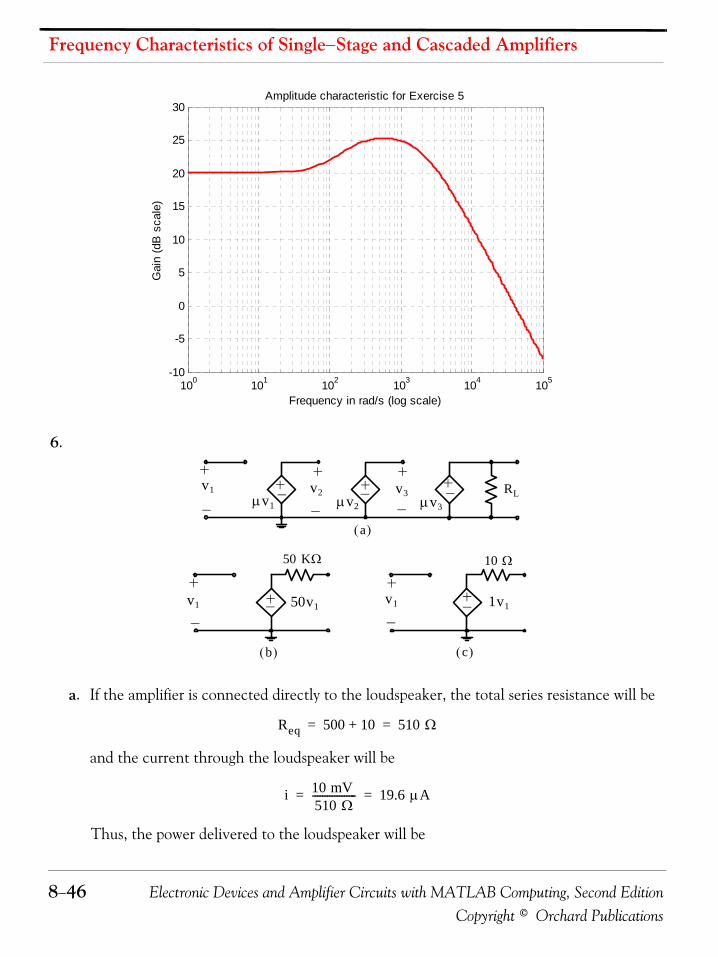
Frequency Characteristics of Single−Stage and Cascaded Amplifiers
8−46 Electronic Devices and Amplifier Circuits with MATLAB Computing, Second EditionCopyright © Orchard Publications
6.
a. If the amplifier is connected directly to the loudspeaker, the total series resistance will be
and the current through the loudspeaker will be
Thus, the power delivered to the loudspeaker will be
100
101
102
103
104
105
-10
-5
0
5
10
15
20
25
30
Frequency in rad/s (log scale)
Gai
n (d
B s
cale
)
Amplitude characteristic for Exercise 5
v1μv1
50 KΩ
μv2 μv3
RL
10 Ω
v2 v3
50v1v1 v1
a( )
b( ) c( )
1v1
Req 500 10+ 510 Ω= =
i 10 mV 510 Ω------------------ 19.6 μA= =
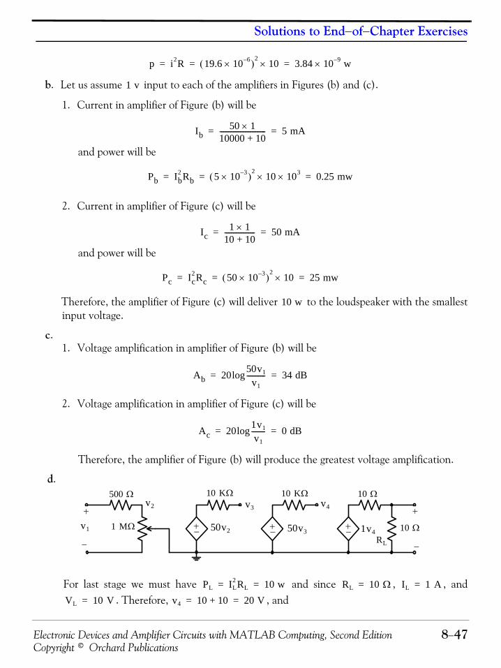
Electronic Devices and Amplifier Circuits with MATLAB Computing, Second Edition 8−47Copyright © Orchard Publications
Solutions to End−of−Chapter Exercises
b. Let us assume input to each of the amplifiers in Figures (b) and (c).
1. Current in amplifier of Figure (b) will be
and power will be
2. Current in amplifier of Figure (c) will be
and power will be
Therefore, the amplifier of Figure (c) will deliver to the loudspeaker with the smallestinput voltage.
c.1. Voltage amplification in amplifier of Figure (b) will be
2. Voltage amplification in amplifier of Figure (c) will be
Therefore, the amplifier of Figure (b) will produce the greatest voltage amplification.
d.
For last stage we must have and since , , and. Therefore, , and
p i2R 19.6 10 6–×( )2 10× 3.84 10 9–× w= = =
1 v
Ib50 1×
10000 10+--------------------------- 5 mA= =
Pb Ib2 Rb 5 10 3–×( )
2 10 103×× 0.25 mw= = =
Ic1 1×
10 10+------------------ 50 mA= =
Pc Ic2 Rc 50 10 3–×( )
2 10× 25 mw= = =
10 w
Ab 20 50v1
v1-----------log 34 dB= =
Ac 20 1v1
v1--------log 0 dB= =
500 Ω
RL
10 Ω
50v3v1 1v4
1 MΩ 10 Ω
10 KΩ 10 KΩv4v3v2
50v2
PL IL2 RL 10 w= = RL 10 Ω= IL 1 A=
VL 10 V= v4 10 10+ 20 V= =

Frequency Characteristics of Single−Stage and Cascaded Amplifiers
8−48 Electronic Devices and Amplifier Circuits with MATLAB Computing, Second EditionCopyright © Orchard Publications
The first and second stages were so chosen as to provide the greatest voltage amplification.
v21 MΩ
1 MΩ 500 Ω+---------------------------------- 10 mV⋅= 10 mV≈
Electronic Devices and Amplifier Circuits with MATLAB Computing, Second Edition 9−1Copyright © Orchard Publications
Chapter 9
Tuned Amplifiers
his chapter begins with an introduction to tuned amplifiers. We will examine the propertiesof various tuned amplifiers that find applications to telecommunications systems employingnarrowband modulated signals. New tools for the analysis and design of tuned amplifiers are
developed.
9.1 Introduction to Tuned Circuits
The amplifiers discussed in previous chapters are sufficient for most applications in which it is notrequired that the signals be transmitted over long distances. Thus they are adequate for audioamplifiers used in public address and home entertainment systems, servomechanisms, automaticpilots, electronic instruments, and a host of similar applications. However, when the signals mustbe transmitted over long distances, as between two cities or between a space vehicle and a groundstation, effective use of the transmission medium requires the use of narrowband systems operatingat high frequencies. Various systems of this kind operate throughout the frequency spectrum from
to about although at the higher end of this range ordinary transistors are notused. For these higher frequencies it is necessary to use tuned amplifiers with RLC coupling toovercome the effects of parasitic capacitances and to provide a filtering operation in the form offrequency−selective amplification. In this section we will introduce the properties of various tunedamplifiers that find application in telecommunication systems.
A tuned amplifier is essentially a bandpass filter.* A passive bandpass filter is constructed with pas-sive devices, i.e., resistors, inductors, and capacitors, and thus it provides no gain. For small sig-nals, active filters with op amps are very popular. Tuned amplifiers can also be designed with bipo-lar junction transistors and MOSFETs, and our subsequent discussion will be based on thesedevices.
When signals must be transmitted over long distances, either by wire or wireless, efficient utiliza-tion of the transmission medium requires the use of high−frequency, narrowband signals. To gen-erate these signals a high−frequency carrier wave, usually a sinusoid, is caused to change instant byinstant in accordance with the information signal to be transmitted. The process by which the car-rier wave is made to change in accordance with the information signal is called modulation. A sinu-soid has three characteristics that can be modulated; they are the amplitude, the frequency, and
* For a thorough discussion on passive and active filters, please refer to Signals and Systems with MATLABApplications, ISBN 978−1−934404−11−9.
T
10 KHz 10 GHz
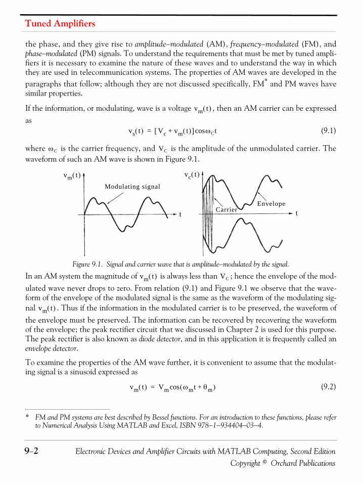
Tuned Amplifiers
9−2 Electronic Devices and Amplifier Circuits with MATLAB Computing, Second EditionCopyright © Orchard Publications
the phase, and they give rise to amplitude−modulated (AM), frequency−modulated (FM), andphase−modulated (PM) signals. To understand the requirements that must be met by tuned ampli-fiers it is necessary to examine the nature of these waves and to understand the way in whichthey are used in telecommunication systems. The properties of AM waves are developed in theparagraphs that follow; although they are not discussed specifically, FM* and PM waves havesimilar properties.
If the information, or modulating, wave is a voltage , then an AM carrier can be expressedas
(9.1)
where is the carrier frequency, and is the amplitude of the unmodulated carrier. Thewaveform of such an AM wave is shown in Figure 9.1.
Figure 9.1. Signal and carrier wave that is amplitude−modulated by the signal.
In an AM system the magnitude of is always less than ; hence the envelope of the mod-ulated wave never drops to zero. From relation (9.1) and Figure 9.1 we observe that the wave-form of the envelope of the modulated signal is the same as the waveform of the modulating sig-nal . Thus if the information in the modulated carrier is to be preserved, the waveform ofthe envelope must be preserved. The information can be recovered by recovering the waveformof the envelope; the peak rectifier circuit that we discussed in Chapter 2 is used for this purpose.The peak rectifier is also known as diode detector, and in this application it is frequently called anenvelope detector.
To examine the properties of the AM wave further, it is convenient to assume that the modulat-ing signal is a sinusoid expressed as
(9.2)
* FM and PM systems are best described by Bessel functions. For an introduction to these functions, please referto Numerical Analysis Using MATLAB and Excel, ISBN 978−1−934404−03−4.
vm t( )
vs t( ) Vc vm t( )+[ ] ωCtcos=
ωC VC
vm t( )
t t
vc t( )
Modulating signal
Carrier Envelope
vm t( ) VC
vm t( )
vm t( ) Vm ωmt θm+( )cos=
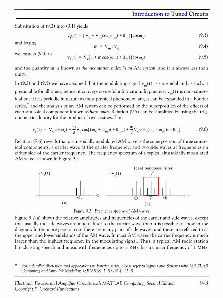
Electronic Devices and Amplifier Circuits with MATLAB Computing, Second Edition 9−3Copyright © Orchard Publications
Introduction to Tuned Circuits
Substitution of (9.2) into (9.1) yields
(9.3)and letting
(9.4)we express (9.3) as
(9.5)
and the quantity is known as the modulation index in an AM system, and it is always less thanunity.
In (9.2) and (9.5) we have assumed that the modulating signal is sinusoidal and as such, it
predictable for all times; hence, it conveys no useful information. In practice, is non−sinuso-idal but if it is periodic in nature as most physical phenomena are, it can be expanded in a Fourierseries,* and the analysis of an AM system can be performed by the superposition of the effects ofeach sinusoidal component known as harmonics. Relation (9.5) can be simplified by using the trig-onometric identity for the product of two cosines. Thus,
(9.6)
Relation (9.6) reveals that a sinusoidally modulated AM wave is the superposition of three sinuso-idal components, a carrier wave at the carrier frequency, and two side waves at frequencies oneither side of the carrier frequency. The frequency spectrum of a typical sinusoidally modulatedAM wave is shown in Figure 9.2.
Figure 9.2. Frequency spectra of AM waves
Figure 9.2(a) shows the relative amplitudes and frequencies of the carrier and side waves, exceptthat usually the side waves are much closer to the carrier wave than it is possible to show in thediagram. In the more general case there are many pairs of side waves, and these are referred to asthe upper and lower sidebands of the AM wave. In most AM waves the carrier frequency is muchlarger than the highest frequency in the modulating signal. Thus, a typical AM radio stationbroadcasting speech and music with frequencies up to has a carrier frequency of
* For a detailed discussion and applications in Fourier series, please refer to Signals and Systems with MATLABComputing and Simulink Modeling, ISBN 978−1−934404−11−9.
vs t( ) Vc Vm ωmt θm+( )cos+[ ] ωctcos=
m Vm Vc⁄=
vs t( ) Vc 1 m ωmt θm+( )cos+[ ] ωctcos=
m
vm t( )
vm t( )
vs t( ) Vc ωctcos m2----Vc ωc ωm+( )t θm+[ ]t m
2----Vc ωc ωm–( )t θm–[ ]cos+cos+=
ω ωωc
vs t( ) vs t( )
a( ) b( )
Ideal bandpass filter
5 KHz 1 MHz

Tuned Amplifiers
9−4 Electronic Devices and Amplifier Circuits with MATLAB Computing, Second EditionCopyright © Orchard Publications
and a total bandwidth of centered at . The advantage of AM signals is that theyare narrowband signals; that is, their total bandwidths are small compared to their center frequen-cies. A narrowband allows the transmission of many simultaneous telephone conversations on asingle pair of conductors in a coaxial cable and for the simultaneous use of space by all radiotransmitters.
Figure 9.2(b) shows the frequency spectra of three AM signals indicated as , , and . Eachsignal uses a different carrier frequency, and normally the difference between these frequencies isgreat enough so that the spectra of the signals are completely separated and occupy different fre-quency bands. These signals can be separated by frequency−selective amplification; the idealizedgain characteristic for such an amplifier is indicated in Figure 9.2(b). Amplifiers of this kind arecalled bandpass amplifiers. Tuning a radio receiver is the operation by which the passband of theamplifier is shifted from one place to another in the frequency spectrum. The study of tunedamplifiers in the sections that follow is concerned with the response of the amplifiers to modu-lated waves and with design techniques for obtaining optimum performance. Optimum perfor-mance is concerned with the rejection of adjacent channels as well as with faithful amplificationof the desired channel.
Relation (9.6) shows that a symmetry exists between the upper and lower sidebands of an AMwave. The sidebands have equal amplitudes, and they have phase angles with respect to the car-rier that are equal in magnitude but opposite in sign. If these components are to add up to givethe original AM wave, this symmetry must be preserved. The significance and importance of thissymmetry is illustrated further by the phasor diagrams in Figure 9.3, in which each sinusoidalcomponent of the wave is represented by a rotating vector. If the carrier vector is taken as thereference and is assumed to be stationary, then the upper−sideband vector rotates counterclock-wise at , and the lower−sideband vector rotates clockwise at the same speed.
Figure 9.3. Phasor representation of an AM wave
In Figure 9.3(a) the sum of the two sideband vectors (represented by the dotted line) is at everyinstant colinear with the carrier vector and it gives a sinusoidal variation in the amplitude of thetotal voltage. However, that this result depends on the symmetry between the sidebands. Toillustrate what may happen when the symmetry is destroyed, Figure 9.3(b) shows the case inwhich the sidebands have been shifted out−of−phase in phase with respect to the carrier. Inthis case, the sum of the sideband vectors (represented by the dotted line) is at every instant nor-mal to the carrier vector, and the amplitude of the total voltage becomes almost constant as indi-
10 KHz 1 MHz
1 2 3
ωm rad sec⁄
a( ) b( ) c( )
ωm
VC VC
ωm
ωm ωm
90°

Electronic Devices and Amplifier Circuits with MATLAB Computing, Second Edition 9−5Copyright © Orchard Publications
Introduction to Tuned Circuits
cated in Figure 9.3(c) where the dotted vectors represent the vector sum of the carrier and thesidebands. When the condition of Figure 9.3(c) occurs, the signal recovered by an envelope detec-tor at the receiving end is very small, and it is badly distorted. Just about all radio signals, whentransmitted over long distances, are subject to this kind of fading and distortion as a result of theproperties of the transmission medium.
System performance can be improved in this respect by transmitting only one of the two side-bands; with single−sideband systems the need for coherence between two sidebands is eliminated.Single sideband systems are discussed in communications systems text, but our intent here is toillustrate that poorly designed amplifiers can degrade the signal. Ideally, then, amplifiers for AMsignals should provide uniform amplification over the band of frequencies occupied by the signal,and they should provide no phase shift in this band. The amplification decreases at high frequen-cies as a result of the parasitic capacitances in the tuned amplifier. It also decreases at low frequen-cies because of the presence of coupling capacitors. In a properly designed tuned circuit, theamplification at the ends of the band of frequencies occupied by the signal should not be less than70 percent of the amplification in the center of the band.
The no phase shift requirement stated above can be somewhat controlled by the fact that a linearphase−shift characteristIc produces a pure delay in the envelope waveform without distorting it.This fact can be illustrated by considering a modulated signal consisting of the sum of a number ofsinusoids of frequencies , not necessarily harmonically related, such that
(9.7)
Substitution of (9.7) into (9.1) yields
(9.8)
The frequency spectrum for this signal is similar to the spectra shown in Figure 9.2 except that inthis case each sideband contains a sinusoidal component corresponding to each sinusoidal compo-nent of the modulating signal; each pair of sideband components exhibits the symmetry discussedabove.
If the modulating signal is allowed a constant time delay T, then (9.7) becomes
(9.9)
or
(9.10)
Since T is a constant, it follows from (9.10) that imposing a constant time delay on is equiv-alent to imposing a lagging phase shift on each sinusoIdal component, proportional to the fre-
ω1 ω2 ω3 …, , ,
vm t( ) V1 ω1t θ1–( )cos V2 ω2t θ2–( )cos V3 ω3t θ3–( )cos …+ + +=
vs t( ) Vc ωctcos 12---V1 ωc ω1+( )t θ1–[ ] 1
2---V1 ωc ω1–( )t θ1–[ ]cos+cos+=
+12---V2 ωc ω2+( )t θ2–[ ] 1
2---V2 ωc ω2–( )t θ2–[ ] …+cos+cos
vm t( ) V1 ω1 t T–( ) θ1–[ ]cos V2 ω2 t T–( ) θ2–[ ]cos V3 ω3 t T–( ) θ3–[ ]cos …+ + +=
vm t( ) V1 ω1t ω1T– θ1–( )cos V2 ω2t ω2T– θ2–( )coscos V3 ω3t ω3T– θ3–( )cos …+ + +=
vm t( )
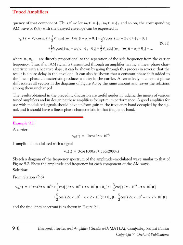
Tuned Amplifiers
9−6 Electronic Devices and Amplifier Circuits with MATLAB Computing, Second EditionCopyright © Orchard Publications
quency of that component. Thus if we let , and so on, the correspondingAM wave of (9.8) with the delayed envelope can be expressed as
(9.11)
where are directly proportional to the separation of the side frequency from the carrierfrequency. Thus, if an AM signal is transmitted through an amplifier having a linear phase char-acteristic with a negative slope, it can be shown by going through this process in reverse that theresult is a pure delay in the envelope. It can also be shown that a constant phase shift added tothe linear phase characteristic produces a delay in the carrier. Alternatively, a constant phaseshift rotates all vectors in the diagrams of Figure 9.3 by the same amount and leaves the relationsamong them unchanged.
The results obtained in the preceding discussion are useful guides in judging the merits of varioustuned amplifiers and in designing these amplifiers for optimum performance. A good amplifier foruse with modulated signals should have uniform gain in the frequency band occupied by the sig-nal, and it should have a linear phase characteristic in that frequency band.
Example 9.1 A carrier
is amplitude−modulated with a signal
Sketch a diagram of the frequency spectrum of the amplitude−modulated wave similar to that ofFigure 9.2. Show the amplitude and frequency for each component of the AM wave.Solution:
From relation (9.6)
and the frequency spectrum is as shown in Figure 9.4.
ω1T φ1= ω2T φ2=
vs t( ) VC ωCtcos 12---V1 ωC ω1+( )t φ1– θ1–[ ] 1
2---V1 ωC ω1–( )t φ1 θ1+ +[ ]cos+cos+=
+12---V2 ωC ω2+( )t φ2– θ2–[ ] 1
2---V2 ωC ω2–( )t φ2 θ2+ +[ ] …+cos+cos
φ1 φ2 …, ,
vC t( ) 10 2π 106t×cos=
vm t( ) 3 1000πtcos 5 2000πtcos+=
vS t( ) 10 2π 106t×cos 32--- 2π 106× π 103×+( )t θm+[ ]t 3
2--- 2π 106× π 103×–( )t[ ]cos+cos+=
+52--- 2π 106× π 2 103××+( )t θm+[ ]t 5
2--- 2π 106× π 2 103××–( )t[ ]cos+cos
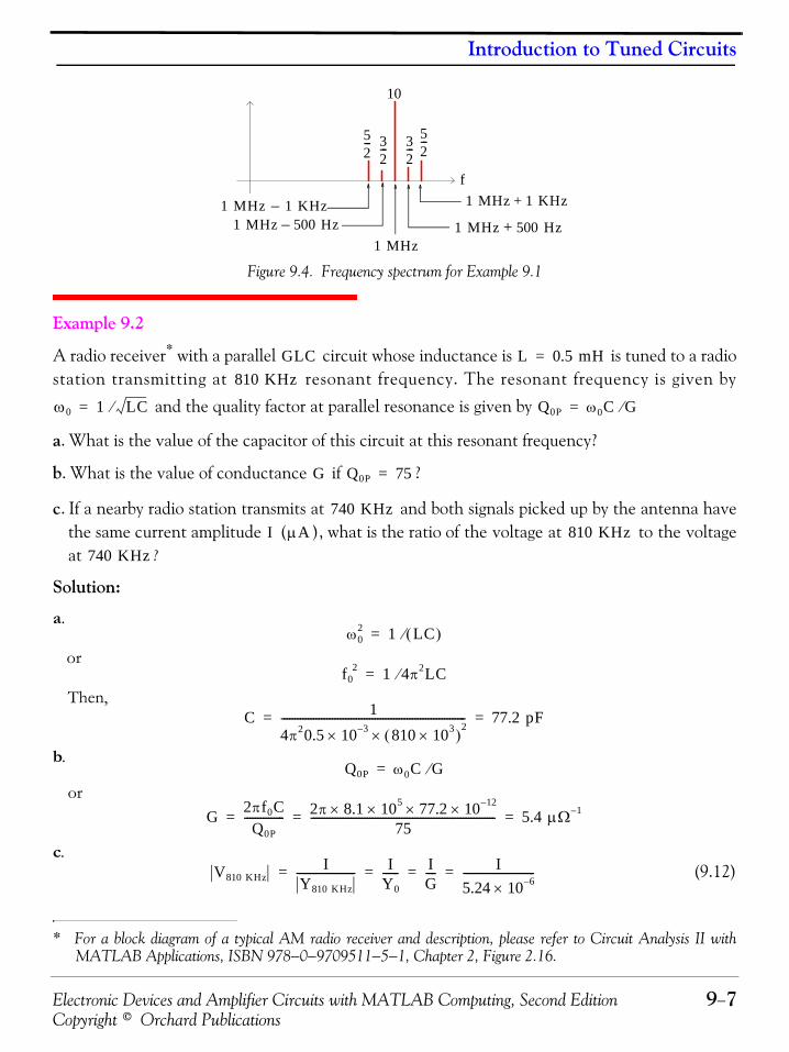
Electronic Devices and Amplifier Circuits with MATLAB Computing, Second Edition 9−7Copyright © Orchard Publications
Introduction to Tuned Circuits
Figure 9.4. Frequency spectrum for Example 9.1
Example 9.2
A radio receiver* with a parallel circuit whose inductance is is tuned to a radiostation transmitting at resonant frequency. The resonant frequency is given by
and the quality factor at parallel resonance is given by
a. What is the value of the capacitor of this circuit at this resonant frequency?
b. What is the value of conductance if ?
c. If a nearby radio station transmits at and both signals picked up by the antenna havethe same current amplitude ( ), what is the ratio of the voltage at to the voltageat ?
Solution:
a.
or
Then,
b.
or
c.(9.12)
* For a block diagram of a typical AM radio receiver and description, please refer to Circuit Analysis II withMATLAB Applications, ISBN 978−0−9709511−5−1, Chapter 2, Figure 2.16.
1 MHz
52---
10
32---3
2---
52---
f
1 MHz 500 Hz– 1 MHz 500 Hz+
1 MHz 1 KHz+1 MHz 1– KHz
GLC L 0.5 mH=
810 KHz
ω0 1 LC⁄= Q0P ω0C G⁄=
G Q0P 75=
740 KHzI μA 810 KHz
740 KHz
ω02 1 LC( )⁄=
f02 1 4π2LC⁄=
C 14π20.5 10 3–× 810 103×( )
2×
--------------------------------------------------------------------- 77.2 pF= =
Q0P ω0C G⁄=
G 2πf0CQ0P
--------------- 2π 8.1 105×× 77.2 10 12–××75
--------------------------------------------------------------------- 5.4 μΩ 1–= = =
V810 KHzI
Y810 KHz---------------------- I
Y0------ I
G---- I
5.24 10 6–×---------------------------= = = =
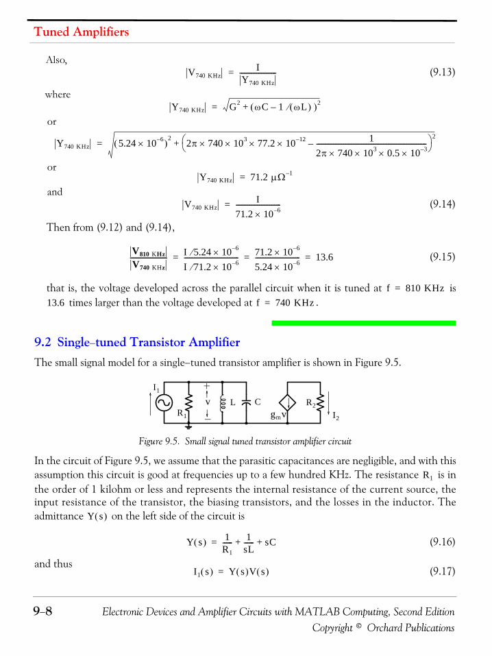
Tuned Amplifiers
9−8 Electronic Devices and Amplifier Circuits with MATLAB Computing, Second EditionCopyright © Orchard Publications
Also,(9.13)
where
or
or
and(9.14)
Then from (9.12) and (9.14),
(9.15)
that is, the voltage developed across the parallel circuit when it is tuned at is times larger than the voltage developed at .
9.2 Single−tuned Transistor AmplifierThe small signal model for a single−tuned transistor amplifier is shown in Figure 9.5.
Figure 9.5. Small signal tuned transistor amplifier circuit
In the circuit of Figure 9.5, we assume that the parasitic capacitances are negligible, and with thisassumption this circuit is good at frequencies up to a few hundred KHz. The resistance is inthe order of 1 kilohm or less and represents the internal resistance of the current source, theinput resistance of the transistor, the biasing transistors, and the losses in the inductor. Theadmittance on the left side of the circuit is
(9.16)
and thus(9.17)
V740 KHzI
Y740 KHz----------------------=
Y740 KHz G2 ωC 1 ωL( )⁄–( )2+=
Y740 KHz 5.24 10 6–×( )2 2π 740 103× 77.2× 10 12–×× 1
2π 740 103× 0.5× 10 3–××------------------------------------------------------------------–⎝ ⎠
⎛ ⎞ 2+=
Y740 KHz 71.2 μΩ 1–=
V740 KHzI
71.2 10 6–×---------------------------=
V810 KHz
V740 KHz---------------------- I 5.24 10 6–×⁄
I 71.2 10 6–×⁄--------------------------------- 71.2 10 6–×
5.24 10 6–×--------------------------- 13.6= = =
f 810 KHz=
13.6 f 740 KHz=
gmvR1
R2I2
I1
CLv
R1
Y s( )
Y s( ) 1R1------ 1
sL------ sC+ +=
I1 s( ) Y s( )V s( )=

Electronic Devices and Amplifier Circuits with MATLAB Computing, Second Edition 9−9Copyright © Orchard Publications
Single−tuned Transistor Amplifier
Also,(9.18)
From (9.12), (9.13), and (9.14) the current gain is
or(9.19)
For convenience, we define two new symbols as
(9.20)
and(9.21)
Substitution of (9.16) and (9.17) into (9.15) yields
(9.22)
The quadratic denominator in (9.18) can be expressed as the product of two linear factors, i.e.,
(9.23)
and we find that(9.24)
and(9.25)
Depending on the values of the circuit parameters, the poles of (9.18) may be either real or com-plex. If they are real, relation (9.19) has the same form as relation (8.71) in Chapter 8; hence thepole−zero pattern and the frequency characteristics of the tuned amplifier with real poles are thesame as those of the RC−coupled amplifier which cannot provide a truly narrow−band characteris-tic. Therefore, in our subsequent discussion we will be concerned with circuit parameters whichwill yield complex poles.
We are also interested in the current gain at the resonant frequency denoted as . From the
parallel network of Figure 9.5, we observe that at parallel resonance inductive susceptance* and
* The inductive susceptance is defined as and the capacitive susceptance as
I2 s( ) gmV s( )–=
Ac
Ac s( )I2 s( )I1 s( )-----------
gm–
1 R1⁄ 1 sL( )⁄ sC+ +--------------------------------------------------= =
Ac s( )gmC
------- ss2 1 RC⁄( )s 1 LC⁄+ +-------------------------------------------------------⋅–=
ω02 1
LC--------=
2α 1RC--------=
Ac s( )gmC
------- ss2 2αs ω0
2+ +---------------------------------⋅–=
Ac s( )gmC
------- ss s1–( ) s s2–( )
-----------------------------------⋅–=
s1 α– α2 ω02–+=
s2 α– α2 ω02––=
Ac0
BL 1 jωL⁄= BC jωC=
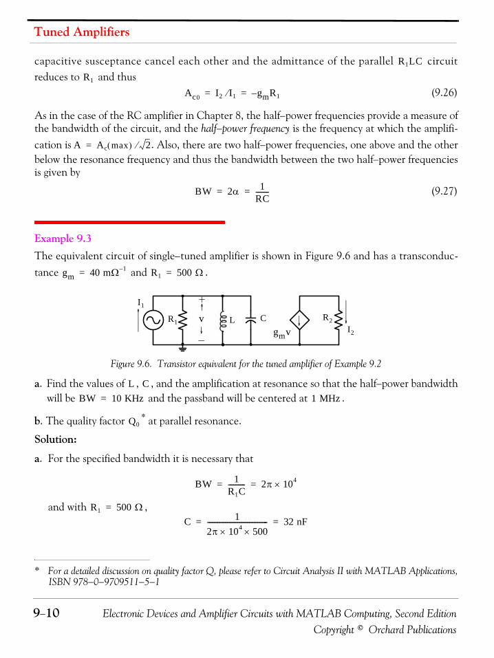
Tuned Amplifiers
9−10 Electronic Devices and Amplifier Circuits with MATLAB Computing, Second EditionCopyright © Orchard Publications
capacitive susceptance cancel each other and the admittance of the parallel circuitreduces to and thus
(9.26)
As in the case of the RC amplifier in Chapter 8, the half−power frequencies provide a measure ofthe bandwidth of the circuit, and the half−power frequency is the frequency at which the amplifi-cation is . Also, there are two half−power frequencies, one above and the otherbelow the resonance frequency and thus the bandwidth between the two half−power frequenciesis given by
(9.27)
Example 9.3 The equivalent circuit of single−tuned amplifier is shown in Figure 9.6 and has a transconduc-tance and .
Figure 9.6. Transistor equivalent for the tuned amplifier of Example 9.2
a. Find the values of , , and the amplification at resonance so that the half−power bandwidthwill be and the passband will be centered at .
b. The quality factor * at parallel resonance.
Solution:
a. For the specified bandwidth it is necessary that
and with ,
* For a detailed discussion on quality factor Q, please refer to Circuit Analysis II with MATLAB Applications,ISBN 978−0−9709511−5−1
R1LCR1
Ac0 I2 I1⁄ gmR1–= =
A Ac max( ) 2⁄=
BW 2α 1RC--------= =
gm 40 mΩ 1–= R1 500 Ω=
gmvR1 R2
I2
I1
CLv
L CBW 10 KHz= 1 MHz
Q0
BW 1R1C---------- 2π 104×= =
R1 500 Ω=
C 12π 104× 500×------------------------------------ 32 nF= =

Electronic Devices and Amplifier Circuits with MATLAB Computing, Second Edition 9−11Copyright © Orchard Publications
Single−tuned Transistor Amplifier
For the specified center frequency
and with ,
The current gain at the resonant frequency is
b. The quality factor at parallel resonance is
In Example 9.2, the very low value of makes a large value of necessary to obtainthe narrow bandwidth , and a relatively high quality factor . Moreover, the verylow value of causes the inductive reactance at to have a very low value of
Fortunately, we can transform values required by the specifications into practical values of the cir-cuit parameters by the use of a transformer. Figure 9.7(a) shows a practical tuned transistor ampli-fier in which a tapped inductor is used as a step−down autotransformer.
Figure 9.7. Impedance transformation in a tuned transistor amplifier and its model
Resistors and provide the necessary biasing but they also include coils in series with theseresistors (not shown) and these coils are known as radio frequency chokes (RFCs). An RFC blocksradio frequencies but passes audio frequencies when both frequencies are applied to the same cir-cuit. The inductors used in the autotransformer have ferrite cores, the coefficient of coupling*
among the turns is close to unity, and the transformation ratio is
ω02 1
LC-------- 2π 106×( )
2 39.5 1012×= = =
C 32 10 9–×=L 1
39.5 1012× 32 10 9–××------------------------------------------------------- 0.8 μH= =
Ac0 gmR1 40 10 3–× 500× 20= = =
Q0
Q0 ω0CR1 2π 106× 32 10 9–× 500×× 100= = =
R1 500 Ω= CBW 10 KHz= Q0
L 1 MHz
ω0L 2π 106× 0.8 10 6–×× 5 Ω= =
gmvR' R2
I2
I1 a⁄
Ca2---- a2L v'
I1
VCC
a( ) b( )
L1
LCE
C
v'
RE
RP RB
RA
vs vsvout
RC
RA RB

Tuned Amplifiers
9−12 Electronic Devices and Amplifier Circuits with MATLAB Computing, Second EditionCopyright © Orchard Publications
(9.28)
where is the total inductance, is the number of turns in the coil, is the inductance por-tion of the coil below the tap, and is the number of turns in the coil below the tap.
When the portion of the circuit on the left of the transformer coil in Figure 9.7(a) is transferredto the right side, the small signal model assumes the form shown in Figure 9.7(b), and the capac-itance and the total inductance are transformed by the factor .
In Figure 9.7(a), the primary side of the step−down autotransformer is the total inductance andthis represents the primary side of the autotransformer, and the secondary side is the portion ofthe coil below the tap. As we know, a practical inductor contains some resistance in series withit. Let the resistance in series with the coil in the primary be denoted as and the resistance inseries with the coil in the secondary be denoted as . The resistance includes the internalresistance of the source supplying the input signal, and when it is referred to the secondary, itassumes the value .
The resistance shown in Figure 9.7(b) represents the parallel combination of with ,that is,
(9.29)
The input signal current is also transformed to as shown in Figure 9.7(b) and since is lessthan unity, we observe that the current amplification is increased by the transformer action.From Figure 9.7(b)
(9.30)
(9.31)
Also,(9.32)
* For a detailed discussion on transformers, please refer to Circuit Analysis II with MATLAB Applications,ISBN 978−0−9709511−5−1
V1
V------ L1
L----- N1
N------ a 1<= = =
L N L1
N1
C L a2
RP
RS RP
a2RP
R' a2RP RS
R' a2RPRS
a2RP RS+------------------------=
I1 a⁄ a
Y' s( ) 1R'----- 1
a2Ls----------- C
a2----s+ +=
I1 s( )a
----------- Y' s( )V' s( )=
I2 s( ) gmV' s( )–=
Ac s( )I2 s( )
I1 s( ) a⁄------------------
gm–
1 R'⁄ 1 a2Ls⁄ Cs a2⁄+ +----------------------------------------------------------= =

Electronic Devices and Amplifier Circuits with MATLAB Computing, Second Edition 9−13Copyright © Orchard Publications
Single−tuned Transistor Amplifier
(9.33)
Therefore, the transformer action leaves the resonant frequency unchanged, but the band-width becomes
(9.34)
The LC combination in Figure 9.7(a) forms a lossless coupling network and if and are fixed,the coupling network can be adjusted for maximum amplification, and this condition occurs whenmaximum power is delivered to . Therefore, maximum amplification is obtained when thevalue of is chosen so that
(9.35)
At resonance, the inductive susceptance and capacitive susceptance cancel out and thus theadmittance is just . Therefore, relation (9.33) reduces to
(9.36)
The quality factor at parallel resonance is
(9.37)
Example 9.4 The equivalent circuit of single−tuned amplifier shown in Figure 9.8 has the transformation ratio
, transconductance , and .
Figure 9.8. Circuit for Example 9.4
a. Find the values of , , and the amplification at resonance so that the half−power bandwidthwill be and the passband will be centered at .
b. The quality factor at parallel resonance.
Ac s( )agm
C---------- s
s2 a2 R'C⁄( )s 1 LC⁄+ +----------------------------------------------------------⋅–=
ω0
BW a2
R'C--------- a2RP RS+
RPRSC------------------------= =
RP RS
RS
aa2RP RS=
R'
AcogmR'
a------------–=
Q0
Q0 ω0CR'=
a 1 20⁄= gm 40 mΩ 1–= R' 500 Ω=
gmv'R' R2
I2
I1 a⁄
Ca2---- a2L v'vs
L CBW 10 KHz= 1 MHz
Q0

Tuned Amplifiers
9−14 Electronic Devices and Amplifier Circuits with MATLAB Computing, Second EditionCopyright © Orchard Publications
Solution:
a. For the specified bandwidth it is necessary that
and with ,
For the specified center frequency
and with ,
The current gain at the resonant frequency is
b. The quality factor at parallel resonance is
9.3 Cascaded Tuned AmplifiersTo achieve higher selectivity it is necessary that tuned amplifiers are connected in cascade bymeans of a coupling capacitor or transformer coupling. When coupling capacitors are used, theyare chosen to act as short circuits in the passband of the amplifier. When two identical stages likethe one shown in Figure 9.5 are cascaded, the overall current gain is given by the square of rela-tion (9.23); hence the zero at the origin and the poles and each appear twice in the overallcurrent gain. The corresponding pole−zero diagram has the form shown in Figure 9.9 where thenumbers in parentheses indicate double poles and zeros. In this form, the two stages are said to besynchronously tuned. We have assumed that the Miller effect is negligible.
9.3.1 Synchronously Tuned AmplifiersThe amplitude characteristic for two synchronously tuned amplifiers is the characteristic for onestage but with the amplification squared at each point. However, the half−power bandwidth isless than the bandwidth of one stage. The phase characteristic is the characteristic for one stagewith the angle multiplied by 2.
BW a2
R'C--------- 2π 104×= =
R' 500 Ω=C 1 400⁄
2π 104× 500×------------------------------------ 80 pF= =
ω02 1
LC-------- 2π 106×( )
2 39.5 1012×= = =
C 80 10 12–×=
L 139.5 1012× 80 10 12–××--------------------------------------------------------- 0.32 mH= =
Ac0
gmR'a
------------ 40 10 3–× 500×1 20⁄
------------------------------------- 400= = =
Q0
Q0 ω0CR' 2π 106× 80 10 12–× 500×× 100= = =
s1 s2
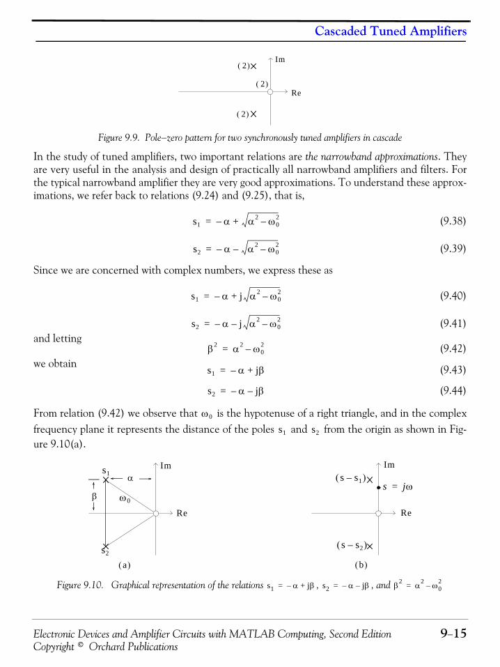
Electronic Devices and Amplifier Circuits with MATLAB Computing, Second Edition 9−15Copyright © Orchard Publications
Cascaded Tuned Amplifiers
Figure 9.9. Pole−zero pattern for two synchronously tuned amplifiers in cascade
In the study of tuned amplifiers, two important relations are the narrowband approximations. Theyare very useful in the analysis and design of practically all narrowband amplifiers and filters. Forthe typical narrowband amplifier they are very good approximations. To understand these approx-imations, we refer back to relations (9.24) and (9.25), that is,
(9.38)
(9.39)
Since we are concerned with complex numbers, we express these as
(9.40)
(9.41)and letting
(9.42)we obtain (9.43)
(9.44)
From relation (9.42) we observe that is the hypotenuse of a right triangle, and in the complexfrequency plane it represents the distance of the poles and from the origin as shown in Fig-ure 9.10(a).
Figure 9.10. Graphical representation of the relations , , and
2( )
2( )
2( )
Re
Im
s1 α– α2 ω02–+=
s2 α– α2 ω02––=
s1 α– j α2 ω02–+=
s2 α– j α2 ω02––=
β2 α2 ω02–=
s1 α– jβ+=
s2 α– jβ–=
ω0
s1 s2
ω0β
αs1
s2
Re
Im
Re
Ims s1–( )
s s2–( )
s jω=
a( ) b( )
s1 α– jβ+= s2 α– jβ–= β2 α2 ω02
–=
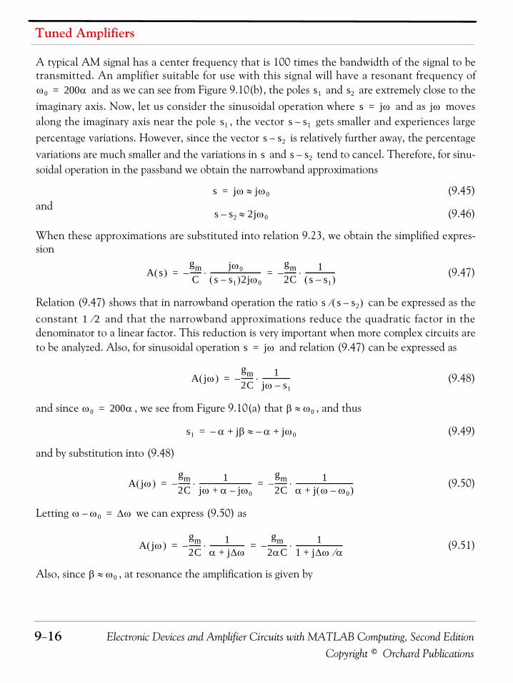
Tuned Amplifiers
9−16 Electronic Devices and Amplifier Circuits with MATLAB Computing, Second EditionCopyright © Orchard Publications
A typical AM signal has a center frequency that is 100 times the bandwidth of the signal to betransmitted. An amplifier suitable for use with this signal will have a resonant frequency of
and as we can see from Figure 9.10(b), the poles and are extremely close to theimaginary axis. Now, let us consider the sinusoidal operation where and as movesalong the imaginary axis near the pole , the vector gets smaller and experiences largepercentage variations. However, since the vector is relatively further away, the percentagevariations are much smaller and the variations in and tend to cancel. Therefore, for sinu-soidal operation in the passband we obtain the narrowband approximations
(9.45)and
(9.46)
When these approximations are substituted into relation 9.23, we obtain the simplified expres-sion
(9.47)
Relation (9.47) shows that in narrowband operation the ratio can be expressed as theconstant and that the narrowband approximations reduce the quadratic factor in thedenominator to a linear factor. This reduction is very important when more complex circuits areto be analyzed. Also, for sinusoidal operation and relation (9.47) can be expressed as
(9.48)
and since , we see from Figure 9.10(a) that , and thus
(9.49)
and by substitution into (9.48)
(9.50)
Letting we can express (9.50) as
(9.51)
Also, since , at resonance the amplification is given by
ω0 200α= s1 s2
s jω= jωs1 s s1–
s s2–
s s s2–
s jω jω0≈=
s s2– 2jω0≈
A s( )gmC
------- jω0
s s1–( )2jω0-----------------------------⋅–
gm2C------- 1
s s1–( )-----------------⋅–= =
s s s2–( )⁄
1 2⁄
s jω=
A jω( )gm2C------- 1
jω s1–----------------⋅–=
ω0 200α= β ω0≈
s1 α– jβ α– jω0+≈+=
A jω( )gm2C------- 1
jω α jω0–+------------------------------⋅–
gm2C------- 1
α j ω ω0–( )+---------------------------------⋅–= =
ω ω0– Δω=
A jω( )gm2C------- 1
α jΔω+--------------------⋅–
gm2αC----------- 1
1 jΔω α⁄+---------------------------⋅–= =
β ω0≈

Electronic Devices and Amplifier Circuits with MATLAB Computing, Second Edition 9−17Copyright © Orchard Publications
Cascaded Tuned Amplifiers
(9.52)
We also recall that the bandwidth is given by
(9.53)
Substitution of (9.52) and (9.53) into (9.51) yields
(9.54)
This relation can also be expressed in terms of the quality factor at resonance, i.e., .Then,
(9.55)
In terms of the bandwidth (relation9.54), the magnitude of the amplification for one stage is
(9.56)
where the subscript unity denotes a single stage. For stages connected in cascade, the magni-tude of the amplification is
(9.57)
The half−power frequency for identical stages connected in cascade occurs when the square ofthe denominator in (9.57) equals 2. Thus, at the half−power frequency
(9.58)
from which
(9.59)
There are two half−power frequencies, one above and one below the resonant frequency. Thebandwidth between these two half−power frequencies is
(9.60)
The square root of this expression is the bandwidth reduction factor for identical stages con-nected in cascade; for two stages it is , for three stages it is , and for four stages it is .
A0 Ac jω0( )gm2C------- 1
jβ α jβ–+--------------------------⋅
gm2αC-----------= = =
BW 2α=
A jω( ) A01
1 j2Δω BW⁄+------------------------------------⋅–=
BW ω0 Q0⁄=
A jω( ) A01
1 j2Q0Δω ω0⁄+----------------------------------------⋅–=
A1 A A011
1 2Δω BW1⁄( )2+------------------------------------------------⋅= =
n
A1n A A01
n 1
1 2Δω BW1⁄( )2+n------------------------------------------------⋅= =
n
1 2ΔωBW1------------⎝ ⎠
⎛ ⎞ 2+ 2=
ΔωBW1
2------------ 21 n⁄ 1–±=
BWn 2Δω BW1 21 n⁄ 1–= =
n0.64 0.51 0.43
Tuned Amplifiers
9−18 Electronic Devices and Amplifier Circuits with MATLAB Computing, Second EditionCopyright © Orchard Publications
Example 9.5 Two synchronously tuned stages connected in cascade are to designed so that the resonant fre-quency will be , and the capacitors will have a value of for each stage.Determine the values of and and the half−power bandwidth for each stage so that the over-all half−power bandwidth will be .
Solution:
The half−power bandwidth of each stage can be determined from relation (9.60), the values of
from the relation and the values of from . For convenience, we willlet the following MATLAB script do the calculations for us.
BWn=2*pi*10^5; C=25*10^(−12); L=1/((2*pi*25*10^6)^2*C); n=2;...BW1= BWn/sqrt(2^(1/n)−1); BWf=BW1/(2*pi); R=1/(BW1*C); fprintf(' \n');...fprintf('C = %5.2e F \t',C);... fprintf('L = %5.2e H \t',L);...fprintf('BW1 = %5.2e rad/sec \t', BW1); fprintf(' \n');...fprintf('BWf = %5.2e Hz \t', BWf);...fprintf('R = %5.2e Ohms \t', R); fprintf(' \n')
Upon execution of this script, MATLAB displays the following results:
C = 2.50e-011 F L = 1.62e-006 H BW1 = 9.76e+005 rad/sec BWf = 1.55e+005 Hz R = 4.10e+004 Ohms
The half−power bandwidth of each stage is and, as expected, is larger than the overallhalf−power bandwidth of .
Synchronous tuning for two stages connected in cascade does not provide the best approxima-tion to the ideal bandpass. As stated above, the bandwidth reduction for synchronous tuning oftwo stages connected in cascade is about and this is confirmed by the ratio
. Figure 9.11 shows the frequency response of a synchronous tuning for twostages in cascade in comparison to a single stage.
9.3.2 Stagger−Tuned Amplifiers
We can obtain a much better approximation by staggering the tuning of the stages to produce apole−zero configuration like the one shown in Figure 9.12.
f0 25 MHz= C 80 pF =
L R100 KHz
R
BW1 1 RC⁄= L ω02 1 LC⁄=
155 KHz100 KHz
0.64100 KHz 155 KHz⁄

Electronic Devices and Amplifier Circuits with MATLAB Computing, Second Edition 9−19Copyright © Orchard Publications
Cascaded Tuned Amplifiers
Figure 9.11. Frequency responses for single stage and two synchronously tuned amplifiers.
Figure 9.12. Pole−zero pattern and amplitude characteristic for two stagger−tuned amplifiers
Poles and in Figure 9.12(a) are the poles one of the stages, and poles and are the polesof the other stage; all four poles lie on a line parallel to the imaginary axis. With this arrangement,the amplitude characteristic of the stagger−tuned amplifier will be shown in Figure 9.12(b). Weobserve that the passband of such stagger−tuned amplifier is wider and flatter than the passband ofthe synchronously tuned amplifier.
The top flatness of the characteristic depends on the spacing between the poles in Figure 9.12(a),and it is under the control of the designer. Consider, for example the relations (9.20) and (9.21)which are repeated below for convenience, and the pole−zero pattern of Figure 9.10(a).
(9.61)
(9.62)
From relation (9.62) we observe that if and remain constant, the spacing from the imagi-nary axis remains constant also. From relation (9.61) we observe that a change in will result in
Single stage response
Overall response for twosynchronously tuned amplifiers
ω (log scale)ω0
Ac (dB scale)
Overall response for two
Single stage responses
stagger tuned amplifiers
ω (log scale)ω0
Ac (dB scale)
Re
a( ) b( )
Im
2( )
s1s3
s4s2
s1 s2 s3 s4
ω02 1
LC--------=
2α 1RC--------=
R C αL
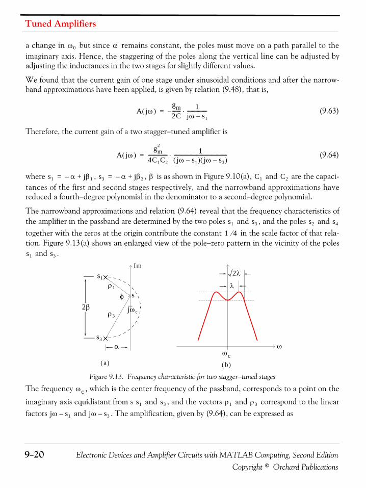
Tuned Amplifiers
9−20 Electronic Devices and Amplifier Circuits with MATLAB Computing, Second EditionCopyright © Orchard Publications
a change in but since remains constant, the poles must move on a path parallel to theimaginary axis. Hence, the staggering of the poles along the vertical line can be adjusted byadjusting the inductances in the two stages for slightly different values.
We found that the current gain of one stage under sinusoidal conditions and after the narrow-band approximations have been applied, is given by relation (9.48), that is,
(9.63)
Therefore, the current gain of a two stagger−tuned amplifier is
(9.64)
where , , is as shown in Figure 9.10(a), and are the capaci-tances of the first and second stages respectively, and the narrowband approximations havereduced a fourth−degree polynomial in the denominator to a second−degree polynomial.
The narrowband approximations and relation (9.64) reveal that the frequency characteristics ofthe amplifier in the passband are determined by the two poles and , and the poles and together with the zeros at the origin contribute the constant in the scale factor of that rela-tion. Figure 9.13(a) shows an enlarged view of the pole−zero pattern in the vicinity of the poles
and .
Figure 9.13. Frequency characteristic for two stagger−tuned stages
The frequency , which is the center frequency of the passband, corresponds to a point on the
imaginary axis equidistant from s and , and the vectors and correspond to the linearfactors and . The amplification, given by (9.64), can be expressed as
ω0 α
A jω( )gm2C------- 1
jω s1–----------------⋅–=
A jω( )gm
2
4C1C2---------------- 1
jω s1–( ) jω s3–( )-------------------------------------------⋅=
s1 α– jβ1+= s3 α– jβ3+= β C1 C2
s1 s3 s2 s4
1 4⁄
s1 s3
αs3
s1
ρ1
ρ3
s
Im
2β
λ
ωcω
jωc
2λ
a( ) b( )
φ
ωc
s1 s3 ρ1 ρ3
jω s1– jω s3–
Electronic Devices and Amplifier Circuits with MATLAB Computing, Second Edition 9−21Copyright © Orchard Publications
Cascaded Tuned Amplifiers
(9.65)
As the variable moves along the imaginary axis, the area of the triangle remainsconstant and its value is
(9.66)
The area can also be expressed in trigonometric form as
(9.67)
and from (9.66) and (9.67)(9.68)
Substitution of (9.68) into (9.65) yields
(9.69)
The poles for the two stages have the same real parts, and thus relation(9.69) can be expressed as
(9.70)
where is the resonant amplification of two stages with synchronous tuning. Therefore, in
relation (9.70), is the only factor that varies with changes in .
If is less than , a circle with center at the middle of the line joining poles and that is par-allel to the imaginary axis and with radius , this circle will intersect the imaginary axis at twopoints, as shown by the dotted semicircle in Figure 9.13(a), and the amplitude characteristic hastwo peaks as shown in Figure 9.13(b). The amplification at the peaks occurs when andthus
(9.71)
In general,(9.72)
If is greater than , the semicircle does not intersect the imaginary axis and the amplitudecharacteristic has only one peak; it is located at and it is less than .The frequencies at which the double peaks occur are denoted as
(9.73)
and since the radius of the semicircle is , it follows that
Agm
2
4C1C2---------------- 1
ρ1ρ3-----------⋅=
s jω= s1 s s3
a αβ=
a 12---ρ1ρ3 φsin=
1ρ1ρ3----------- φsin
2αβ-----------=
Agm
2
4C1C2---------------- φsin
2αβ-----------⋅=
α 1 2R1C1⁄ 1 2R2C2⁄= =
A gm2 R1R2
α2β------ φsin=
gm2 R1R2
φsin ω
α β s1 s3
β
φsin 1=
Ap gm2 R1R2
α2β------=
A Ap φsin=
α βω ωc= Ap
ωp ωc λ±=
β
Tuned Amplifiers
9−22 Electronic Devices and Amplifier Circuits with MATLAB Computing, Second EditionCopyright © Orchard Publications
(9.74)
The triple−point frequencies are the frequencies outside the double peaks at which the amplifi-cation has the same value as at the center frequency are obtained by
(9.75)
Let be the value of the angle when . Then, the amplification at the center fre-
quency, denoted as is(9.76)
The peak−to−valley ratio for the double−peaked amplitude characteristic is
(9.77)
The angle is related to the pole positions by
(9.78)
When the amplifier is adjusted so that , the semicircle is tangent to the imaginary axis,and the amplitude characteristic is maximally flat. In this case, the amplifier is also said to be flat−staggered, and this condition marks the transition from the overstaggered (double peaks) to theunderstaggered adjustment. We are mostly interested on the flat−staggered and the overstaggeredcases.
In all of the amplifiers studied up to this point, the half−power bandwidth has been related in asimple way to the circuit parameters. In the case of the overstaggered pair of tuned stages, how-ever, a simpler and in some respects more useful measure of the bandwidth is the so−called triple−point bandwidth shown by the dotted lines in Figure 9.13(b). It is defined as
* (9.79)From relations (9.74) and (9.79)
(9.80)
It is convenient to express relation (9.80) in terms of the design parameter which isrelated to the peak−to−valley ratio in relation (9.77). Rearranging relation (9.80) we obtain
(9.81)
* We reserve the notation for the bandwidth and we will use for the triple−point bandwidth.
λ2 β2 α2–=
ωt
ωt ωc 2λ±=
φc φ ω ωc=
Ac
Ac Ap φcsin=
ApAc------- 1
φcsin-------------=
φc
φc2-----tan β
α--- r= =
α β=
W 2 2λ=
BW 3 dB– W
W2 8λ2 8 β2 α2–[ ]= =
r β α⁄=
W2α-------⎝ ⎠
⎛ ⎞2
2 βα---⎝ ⎠
⎛ ⎞2
1– 2 r2 1–( )= =
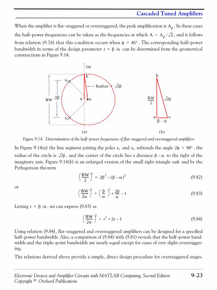
Electronic Devices and Amplifier Circuits with MATLAB Computing, Second Edition 9−23Copyright © Orchard Publications
Cascaded Tuned Amplifiers
When the amplifier is flat−staggered or overstaggered, the peak amplification is . In these cases
the half−power frequencies can be taken as the frequencies at which , and it follows
from relation (9.76) that this condition occurs when . The corresponding half−powerbandwidth in terms of the design parameter can be determined from the geometricalconstructions in Figure 9.14.
Figure 9.14. Determination of the half−power frequencies of flat−staggered and overstaggered amplifiers
In Figure 9.14(a) the line segment joining the poles and subtends the angle , the
radius of the circle is , and the center of the circle lies a distance to the right of theimaginary axis. Figure 9.14(b) is an enlarged version of the small right triangle and by thePythagorean theorem
(9.82)
or(9.83)
Letting , we can express (9.83) as
(9.84)
Using relation (9.84), flat−staggered and overstaggered amplifiers can be designed for a specifiedhalf−power bandwidth. Also, a comparison of (9.84) with (9.81) reveals that the half−power band-width and the triple−point bandwidth are nearly equal except for cases of very slight overstagger-ing.
The relations derived above provide a simple, direct design procedure for overstaggered stages.
Ap
A Ap 2⁄=
φ 45°=
r β α⁄=
s3
s1
a
Im
2β
a( ) b( )
b
o
Radius 2β=
a o
b
2βBW
β α–
BW2
----------
s1 s3 2φ 90°=
2β β α–
oab
BW2
----------⎝ ⎠⎛ ⎞2
2β2 β α–( )2–=
BW2α----------⎝ ⎠
⎛ ⎞2 βα---⎝ ⎠
⎛ ⎞2 2β
α------ 1–+=
r β α⁄=
BW2α----------⎝ ⎠
⎛ ⎞2r2 2r 1–+=

Tuned Amplifiers
9−24 Electronic Devices and Amplifier Circuits with MATLAB Computing, Second EditionCopyright © Orchard Publications
The design requirements specify the center frequency , the triple−point bandwidth , and
the peak−to−valley ratio .These specifications are sufficient to define the poles of the
amplitude gain , and hence the circuit parameters. Specifically, the ratio defines
through relations (9.77) and (9.78). Then, relation (9.81) gives the required value of, and the required value of is obtained from the relation . Thus, the two of the three
parameters , , and are determined, and the third can be chosen as desired to satisfy theother requirement as it was illustrated in the previous examples.
Example 9.6 A transistorized two−stage stagger−tuned amplifier has a pole−zero pattern like the one shown inFigure 9.13. The pertinent dimensions are , , and .
Both transistors have a transconductance of , and the total shunt resistance in
each stage is . Find the peak amplification , the peak−to−valley ratio
, the triple−point bandwidth , the half−power bandwidth , and the triple−point fre-quencies. Solution:
The peak amplification is found from (9.71), i.e.,
From relation (9.78)
The peak−to−valley ratio is given by relation (9.77)
Therefore, the amplifiers are overstaggered.
The triple−point bandwidth , is given by relation (9.79), i.e., where from relation(9.74)
ωc W
Ap Ap⁄
A Ap Ap⁄
r β α⁄=
α β β αr=
R L C
ωp 106 rad/s= α 1500 rad/s= β 2500 rad/s=
gm 40 mΩ 1–=
R1 R2 0.75 KΩ= = Ap
Ap Ac⁄ W BW
Ap
Ap gm2 R1R2
α2β------ 40 10 3–×( )
2 0.75 103×( )2 1.5
5-------×× 270= = =
φc2-----tan β
α--- r 2.5
1.5------- 5
3---= = = =
φc 2⁄ 5 3⁄( )1–tan 59°= =
φc 118°=
Ap Ac⁄
ApAc------- 1
φcsin------------- 1
118°sin------------------- 1.13= = =
W W 2 2λ=

Electronic Devices and Amplifier Circuits with MATLAB Computing, Second Edition 9−25Copyright © Orchard Publications
Cascaded Tuned Amplifiers
The half−power bandwidth is given by relation (9.83), i.e.,
The triple−point frequencies are given by relation (9.75). Thus,
The procedure for finding all pertinent data, except the values of and , was well illustrated inExample 9.6. The following example illustrates the procedure for finding of and to meet alldesign specifications.
Example 9.7
The pole locations for a two−stage stagger−tuned amplifier and the values of and are asgiven in Example 9.6. Determine the values of and required for each stage.
Solution:
From relation (9.27)
and thus
With , and , we find that
and
λ2 β2 α2– 2.52 1.52–( ) 106× 4 106× (rad/s) 2= = =
λ 2 103 rad/s×=
W 2 2λ 4 2 103× 5.66 103× rad/s= = =
BW
BW2α----------⎝ ⎠
⎛ ⎞2 βα---⎝ ⎠
⎛ ⎞2 2β
α------ 1–+=
BW 2α βα---⎝ ⎠
⎛ ⎞2 2β
α------ 1–+ 2 1.5 103×× 2.5
1.5-------⎝ ⎠
⎛ ⎞2 5
1.5------- 1–+ 6.78 103× rad/s= = =
ωt ωc 2λ± 106 2 2× 10³×±= =
ωt1 1.003 106 rad/s×= ωt2 0.997 106 rad/s×=
L CL C
R1 R2
L C
BW 2α 1RC--------= =
2α 1R1C1------------ 1
R2C2------------= =
ωc 106 rad/s= α 1500 rad/s= R1 R2 0.75 KΩ= =
C1 C21
2αR1------------- 1
2αR2------------- 1
3 103× 0.75 103××------------------------------------------------ 0.44 μF= = = = =

Tuned Amplifiers
9−26 Electronic Devices and Amplifier Circuits with MATLAB Computing, Second EditionCopyright © Orchard Publications
Figure 9.15 shows the normalized amplitude characteristics for two tuned stages under four dif-ferent adjustments.
Figure 9.15. Amplitude characteristics for two tuned stages with different degrees of staggering
For the curves in Figure 9.15, is held constant while is increased in steps. Curve 1 is for syn-chronous tuning, Curve 2 is for understaggering with , Curve 3 is for flat staggering, andCurve 4 is for overstaggering with . The half−power bandwidths are indicated bythe solid dots on these curves.
For the flat−staggered case , , and . Thus, from relations (9.71) and (9.72)we obtain
(9.85)
Letting denote the bandwidth of two stages with flat staggering and the band-width of one of the stages, from (9.84) we obtain
(9.86)
The gain−bandwidth product for the flat−staggered amplifier is given by
(9.87)
L11
ωt12 C1
-------------- 10.9972 1012 0.44 10 6–×××----------------------------------------------------------------- 2.28 μH= = =
L21
ωt22 C2
-------------- 11.0032 1012 0.44 10 6–×××----------------------------------------------------------------- 2.27 μH= = =
1 2 3 4
AAc-------
ωcω
α βφc 70°=
Ap Ac⁄ 1.1=
β α= r 1= φcsin 1=
Ac Ap12---gm
2 R1R2= =
Bfs BW 3 dB–
Bfs 2 2BW=
AcBfs 1 2⁄( ) gm2 R1R2( )BW=

Electronic Devices and Amplifier Circuits with MATLAB Computing, Second Edition 9−27Copyright © Orchard Publications
Cascaded Tuned Amplifiers
For two synchronously tuned stages we denote the bandwidth of two stages as . Then, for thegain−bandwidth product, using relation (9.60) we obtain
(9.88)
The foregoing discussion of stagger−tuned amplifiers considers only the case in which the poles arestaggered along a line parallel to the imaginary axis. If the poles do not lie on the same verticalline, skewed frequency characteristics result, and, in accordance with the discussion in Section9.1, this fact may cause distortion of the envelopes of AM signals.
9.3.3 Three or More Tuned Amplifiers Connected in Cascade
When three or more tuned stages are to be connected in cascade, the relations encountered aresimilar in many respects to those encountered in the two−stage case. In particular, for narrowbandamplifiers the frequency characteristics are determined entirely by the poles lying near the seg-ment of the imaginary axis corresponding to the passband. Thus, in the usual case, the zeros at theorigin and the poles in the lower half plane contribute only a constant to the gain in the narrowpassband. By a more extensive treatment* it can be shown that for a maximally flat amplitudecharacteristic, the poles of the signal gain must be uniformly spaced on a semicircle having its cen-ter on the imaginary axis. The amplitude characteristics for one, three, and five stages are shownin Figure 9.16.
Figure 9.16. Maximally flat multistage tuned amplifiers
In Figure 9.16, The center frequency of the passband corresponds to the center of the circle onwhich the poles lie, and no matter how many stages are cascaded, the half−power frequencies arethe frequencies at which the circle intersects the imaginary axis. The more stages cascaded in thisway, the flatter the amplitude characteristic in the passband and the steeper the characteristic atthe edges of the band. The distribution of poles producing these characteristics is known as theButterworth configuration.
* For a detailed discussion on this topic, please refer to Signals and Systems with MATLAB Computing and Sim-ulink Modeling, ISBN 978−1−934404−11−9.
Bsyn
AcBsyn A12BW1 21 2⁄ 1– 0.64 gm
2 R1R2( ) BW( )= =
1
53
A
ωcω
ωc

Tuned Amplifiers
9−28 Electronic Devices and Amplifier Circuits with MATLAB Computing, Second EditionCopyright © Orchard Publications
9.4 Summary• A tuned amplifier is essentially a bandpass filter. A passive bandpass filter is constructed with
passive devices, i.e., resistors, inductors, and capacitors, and thus it provides no gain. Forsmall signals, active filters with op amps are very popular. Tuned amplifiers can also bedesigned with bipolar junction transistors and MOSFETs.
• The analysis and design of tuned amplifiers is greatly facilitated with the small signal models.
• For a single stage tuned amplifier the current gain at the resonant frequency is given by
and the bandwidth between the two half−power frequencies is given by
• In the design of tuned amplifiers, we can transform values required by the specifications intopractical values of the circuit parameters by the use of a transformer.
• A radio frequency choke (RFC) blocks radio frequencies but passes audio frequencies whenboth frequencies are applied to the same circuit.
• Tuned amplifiers are connected in cascade to achieve higher selectivity.
• When two identical stages are cascaded, the two stages are said to be synchronously tuned.
• The amplitude characteristic for two synchronously tuned amplifiers is the characteristic forone stage but with the amplification squared at each point.
• In the study of tuned amplifiers, two important relations are the narrowband approximations.They are very useful in the analysis and design of practically all narrowband amplifiers and fil-ters.
• For synchronously tuned amplifiers the bandwidth between the half−power points is given by
• The passband of such stagger−tuned amplifier is wider and flatter than the passband of thesynchronously tuned amplifier and thus provides a better approximation to the ideal band-pass.
• The amplification at resonance for a two stagger−tuned amplifier is given by
where is the resonant amplification of two stages with synchronous tuning.
Ac0 I2 I1⁄ gmR1= =
BW
BW 2α 1 RC⁄= =
BWn 2Δω BW1 21 n⁄ 1–= =
A gm2 R1R2
α2β------ φsin=
gm2 R1R2

Electronic Devices and Amplifier Circuits with MATLAB Computing, Second Edition 9−29Copyright © Orchard Publications
Summary
• For stagger−tuned amplifiers, the frequencies at which the double peaks occur given by
• For stagger−tuned amplifiers, the frequencies outside the double peaks at which the amplifica-tion has the same value as at the center frequency are obtained by
• For stagger−tuned amplifiers adjusted so that , the amplifier is also said to be flat−stag-gered, and this condition marks the transition from the overstaggered (double peaks) to theunderstaggered adjustment. We are mostly interested on the flat−staggered and the overstag-gered cases.
• For an overstaggered pair of tuned stages the triple−point bandwidth is defined as
and half−power bandwidth is given by
• For uniform amplification over a wide band of frequencies we can cascade 3 or more amplifierswhere the distribution of poles produce characteristics is known as the Butterworth configura-tion.
ωp ωc λ±=
ωt ωc 2λ±=
α β=
W 2 2λ=
BW
BW2α----------⎝ ⎠
⎛ ⎞2 βα---⎝ ⎠
⎛ ⎞2 2β
α------ 1–+=

Tuned Amplifiers
9−30 Electronic Devices and Amplifier Circuits with MATLAB Computing, Second EditionCopyright © Orchard Publications
9.5 Exercises1. The small−signal model for a single−tuned amplifier is shown below, and for this model, it is
known that and .
a. Determine the values of and so that the amplifier will have a resonant frequency of and a half−power bandwidth of .
b. Determine the current gain , i.e., the current gain at the resonant frequency.
2. For the incremental model of a typical MOSFET tuned circuit below,
By a procedure similar to that in Section 9.2, we can show that the resonant frequency, thehalf−power frequency, and the voltage gain at resonance are given by the relations
a. Find suitable values for circuit parameters so that the half−power bandwidth will be the, and the passband will be centered at .
b. Find the voltage amplification at resonance.
c. Find the quality factor at resonance.
3. Two synchronously tuned stages are connected in cascade and the transconductance of bothtransistors used is where and are to designed so thatthe resonant frequency will be . Find the resonant amplification.
4. A two−stage flat−staggered tuned amplifier is to designed with two transistors each withtransconductance where and are to designed sothat the resonant frequency will be . Find the resonant amplification.
gm 40 mΩ 1–= R1 1 KΩ=
gmvR1
R2I2
I1
CLv
L C100 KHz 5 KHz
Ac0 I2 I1⁄=
gm 5 mΩ 1–=
gmV1
R1R2 V2V1 CL
ω02 1
LC--------= BW 2α 1
R1C----------= = Av0 gmR1=
10 KHz 1 MHz
gm 40 mΩ 1–= R1 1 KΩ= R2 1.5 KΩ=
fc 25 MHz=
gm 40 mΩ 1–= R1 1 KΩ= R2 1.5 KΩ=
fc 25 MHz=

Electronic Devices and Amplifier Circuits with MATLAB Computing, Second Edition 9−31Copyright © Orchard Publications
Solutions to End−of−Chapter Exercises
9.6 Solutions to End−of−Chapter Exercises1.
a. The bandwidth in radians per second is
and with ,
The value of is found from , or . Thus,
b. The current gain at resonance is
2.
a. For the required bandwidth it is necessary that
and for the specified center frequency we must have
For high gain we can choose a large value for . Or, we can choose a large value for toovercome the parasitic capacitances. Let us assume that the parasitic capacitances are ofmore concern to us and choose a capacitor. Then, the bandwidth requirementyields
gmvR1
R2I2
I1
CLv
BW 2α 1RC-------- 2π 5000× 3.14 104×= = = =
R1 1 KΩ=
C 1BW R1⋅-------------------- 1
3.14 104× 103×--------------------------------------- 31.8 nF= = =
L ω02 1 LC⁄= f0
2 1 2πLC⁄=
L 12π 105×( )
2 31.8 10 9–××------------------------------------------------------------- 80 μH= =
Ac0 gmR1 40 mΩ 1– 1 KΩ× 40= = =
gmV1
R1R2 V2V1 CL
BW 2α 1R1C---------- 2π 104×= = =
ω02 1 LC⁄ 2π 106×( )
2= =
R1 C
200 pF

Tuned Amplifiers
9−32 Electronic Devices and Amplifier Circuits with MATLAB Computing, Second EditionCopyright © Orchard Publications
The value of to meet the center−frequency requirement is
b. The voltage gain at the center−frequency is
c. The quality factor at resonance is
3. By relation (9.26) the resonant amplification of the first stage is , and that of the
second stage is . Therefore, the overall gain is
4. By relation (9.85)
As expected this gain is half of that of Exercise 3 where the circuit was designed with synchro-nously tuned stages.
R11
BWC-------------- 1012
2π 104× 200×------------------------------------ 80 KΩ= = =
L
L 1ω0
2C---------- 1012
2π 106×( )2 200×
------------------------------------------- 0.125 mH= ==
Av0 gmR1 5 10 3–× 80 103×× 400= = =
Q0 ω0CR1 2π 106× 200 10 12–× 80 103××× 100= = =
A1 gmR1=
A2 gmR2=
A gm2 R1R2 40 10 3–×( )
2 1 1.5 106××× 60= = =
Ac Ap12---gm
2 R1R212--- 40 10 3–×( )
2 1 1.5 106××× 30= = = =

Electronic Devices and Amplifier Circuits with MATLAB Computing, Second Edition 10−1Copyright © Orchard Publications
Chapter 10
Sinusoidal Oscillators
his chapter begins with an introduction to sinusoidal oscillators. Subsequently, we will dis-cuss the RC phase−shift and LC oscillator families, and we will describe the Armstrong,Hartley, Colpitts, crystal, and the crystal−controlled Pierce oscillators.
10.1 Introduction to OscillatorsAn oscillator may be defined as a class of wave generators that produce sinusoidal, square, triangu-lar, and sawtooth waveforms. Non−sinusoidal oscillators are known as relaxation oscillators. InChapter 5 we introduced the Wien bridge oscillator, and in Chapter 7 the family of multivibrators.In this chapter we will be concerned with oscillators that produce sinusoidal waveforms. An oscil-lator is essentially an amplifier circuit that provides its own input signal. Oscillators are classifiedin accordance with the waveshapes they produce and the circuitry required to produce the desiredoscillations. Henceforth, in this chapter, unless otherwise specified, the term oscillator will mean asinusoidal oscillator.
10.2 Sinusoidal OscillatorsAs the name implies, a sinusoidal oscillator produces a sine−wave output signal. An ideal oscillatorshould produce an output signal with constant amplitude with no variation in frequency. But apractical oscillator cannot meet these criteria, the degree to which the ideal is approacheddepends on the class of amplifier operation, amplifier characteristics, frequency stability, andamplitude stability. Sinusoidal oscillators generate signals ranging from low audio frequencies toultrahigh radio and microwave frequencies. Many low−frequency oscillators use resistors andcapacitors to form their frequency−determining networks and are referred to as RC oscillators.These are used in the audio−frequency range.
Other types of employ inductors and capacitors for its frequency−determining network. These areknown as the LC oscillators and use tank circuits*, are commonly used for the higher radio frequen-cies. They are not suitable for use as extremely low−frequency oscillators because the inductorsand capacitors would be large in size, heavy, and costly to manufacture.
A third type of sinusoidal oscillator is the crystal−controlled oscillator. The crystal−controlled oscil-lator provides excellent frequency stability and is used from the middle of the audio range throughthe radio frequency range.
* The term tank circuit stems from the fact that a network consisting of inductors and capacitors store energysame way as liquids and gases are stored in tanks.
T
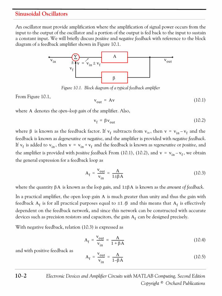
Sinusoidal Oscillators
10−2 Electronic Devices and Amplifier Circuits with MATLAB Computing, Second EditionCopyright © Orchard Publications
An oscillator must provide amplification where the amplification of signal power occurs from theinput to the output of the oscillator and a portion of the output is fed back to the input to sustaina constant input. We will briefly discuss positive and negative feedback with reference to the blockdiagram of a feedback amplifier shown in Figure 10.1.
Figure 10.1. Block diagram of a typical feedback amplifier
From Figure 10.1,(10.1)
where denotes the open−loop gain of the amplifier. Also,
(10.2)
where is known as the feedback factor. If subtracts from , then and thefeedback is known as degenerative or negative, and the amplifier is provided with negative feedback.If is added to , then and the feedback is known as regenerative or positive, and
the amplifier is provided with positive feedback From (10.1), (10.2), and , we obtainthe general expression for a feedback loop as
(10.3)
where the quantity is known as the loop gain, and is known as the amount of feedback.
In a practical amplifier, the open loop gain is much greater than unity and thus the gain withfeedback is for all practical purposes equal to and this means that is effectivelydependent on the feedback network, and since this network can be constructed with accuratedevices such as precision resistors and capacitors, the gain can be designed precisely.
With negative feedback, relation (10.3) is expressed as
(10.4)
and with positive feedback as(10.5)
vin v vin vf±=vout
Σ A
β
vf
±
vout Av=
A
vf βvout=
β vf vin v vin vf–=
vf vin v vin vf+=
v vin vf–=
Afvoutvin---------- A
1 β± A--------------= =
βA 1 β± A
AAf 1 β⁄± Af
Af
Afvoutvin---------- A
1 βA+-----------------= =
Afvoutvin---------- A
1 β– A--------------= =
Electronic Devices and Amplifier Circuits with MATLAB Computing, Second Edition 10−3Copyright © Orchard Publications
Sinusoidal Oscillators
Practically, all amplifiers employ negative feedback, but as we will see shortly, sinusoidal oscillatorsuse positive feedback.
Example 10.1
A certain amplifier has an open−loop gain of at an angle of zero degrees, distortion of ,and normal input voltage of . Determine the effects of negative feedback if the feedback factor
is .
Solution:
For negative feedback and in accordance with relation (10.4) the gain withnegative feedback is
The amount of distortion without feedback is of the normal input voltage of , andwith feedback is
New input voltage with feedback is
The output voltage without feedback is
and the output voltage with feedback is
Actual input voltage to amplifier is
and the reduction in gain expressed in is
Thus, the introduction of negative feedback has reduced the amplifier gain by or we cansay that of feedback has been applied to the input of the amplifier.
A 70 10%1 V
β 0.1
βA 0.1 70× 7= =
AfA
1 βA+----------------- 70
1 7+------------ 8.75= = =
D 10% vin 1 V
Df0.1 1×1 βA+----------------- 0.10
1 7+------------ 0.0125 1.25%= = = =
v'in
v'in vin 1 βA+( ) 1 1 7+( )× 8 V= = =
vout
vout Avin 70 1× 70 V= = =
v'out
v'out Afv'in 8.75 8× 70 V= = =
v
v v'in βv'out– 8 0.1 70×– 1 V= = =
dB
dB 20 AAf-----log 20 70
8.75----------log 18.06 dB= = =
18 dB18 dB
Sinusoidal Oscillators
10−4 Electronic Devices and Amplifier Circuits with MATLAB Computing, Second EditionCopyright © Orchard Publications
Example 10.1 above and Exercise 1 at the end of this chapter illustrate the effects of degenerative(negative) feedback. In our subsequent discussion we will be concerned with regenerative (posi-tive) feedback. Let us again consider relation (10.5) which is repeated below for convenience.
(10.6)
In an oscillator circuit the positive feedback must be large enough to compensate for circuitlosses so that oscillations will be sustained. Moreover, a practical oscillator must oscillate at a pre-determined frequency and thus the oscillator must include a frequency−determining devicewhich essentially is a band−pass filter allowing only the desired frequency to pass. Let us nowassume that at that predetermined frequency the loop gain in relation (10.6) above is veryclose to unity and in this case the closed loop is very large. Accordingly, it is possible to obtaina finite output with a very small input and this is the principle behind the operation of an oscilla-tor.
To find the predetermined frequency to produce sustained oscillations, we express relation(10.6) in the s−domain, that is,
(10.7)
and letting we obtain
(10.8)
To sustain oscillations at the denominator of (10.8) must meet the Barkhausen criterionwhich states that to provide sinusoidal oscillations the magnitude and phase angle of the term
must be such that (10.9)
and(10.10)
10.3 RC OscillatorAn amplifier and an RC network can form an oscillator as shown in Figure 10.2. This oscillator isalso known as phase−shift oscillator. In the oscillator circuit of Figure 10.2 the transistor, being inthe common−emitter configuration, provides phase shift and the three RC sections can beselected that each section will provide shift. Therefore, the total phase shift in that oscillatorwill be and the condition of relation (10.10) will be satisfied. The condi-tion of relation (10.9) can also be satisfied by making the product equal to unity. Forinstance, if we can make and the condition of relation (10.9) will also be sat-isfied.
Afvoutvin---------- A
1 β– A--------------= =
βAAf
ω0
Af s( )Vout s( )Vin s( )------------------ A s( )
1 β s( )– A s( )-----------------------------= =
s jω=
Af jω( )Vout jω( )Vin jω( )---------------------- A jω( )
1 β jω( )– A jω( )-------------------------------------= =
ω ω0=
β jω( )A jω( )β jω0( )A jω0( ) 1≥
β jω0( )∠ A jω0( )∠+ 2πn= n 1 2 3 …, , ,=
180°60°
3 60°× 180°+ 360°=
βAA 10= β 1 10⁄=

Electronic Devices and Amplifier Circuits with MATLAB Computing, Second Edition 10−5Copyright © Orchard Publications
LC Oscillators
Figure 10.2. Simple form of an RC oscillator
The output of the oscillator contains only a single sinusoidal frequency. When the oscillator ispowered on, the loop gain is greater than unity and the amplitude of the oscillations willincrease. Eventually, a level is reached where the gain of the amplifier decreases, and the value ofthe loop gain decreases to unity and constant amplitude oscillations are sustained. The frequencyof oscillations is determined by the values of resistance and capacitance in the three sections.Variable resistors and capacitors are usually employed to provide tuning in the feedback networkfor variations in phase shift. For an RC phase−shift oscillator, the amplifier is biased for Class Aoperation to minimize distortion of the signal.
For the RC oscillator of Figure 10.2, the frequency of oscillation is given by
(10.11)
where is the transistor power gain and the values of the resistors and the transistor gain aresuch that the following relation is satisfied.
(10.12)
In general, for an RC phase−shift oscillator the frequency of oscillation (resonant frequency) canbe approximated from the relation
(10.13)
where is the number of RC sections.
10.4 LC OscillatorsThe LC type of oscillators use resonant circuits. As we know, a resonant circuit stores energy alter-nately in the inductor and capacitor. However, every circuit contains some resistance and thisresistance causes reduction in the amplitude of the oscillations. To sustain oscillations with con-stant amplitude it is necessary to use regenerative feedback. Figure 10.3 shows a block diagram ofa typical LC oscillator. In an LC oscillator the sinusoidal signal is generated by the action of aninductor and a capacitor. The feedback signal is coupled from the LC tank of the oscillator circuit
C C CR
R R
RL
βA
ω01
C 4RRL GR2+----------------------------------------=
G β
β 23 29RRL
---------- 4RL
R---------+ +=
ω01
RC n---------------=
n

Sinusoidal Oscillators
10−6 Electronic Devices and Amplifier Circuits with MATLAB Computing, Second EditionCopyright © Orchard Publications
by using a coil (tickler* or a coil pair) as shown in Figure 10.4(a) and 10.4(b) or by using a capac-itor pair in the tank circuit and tap the feedback signal between them as shown in Figure 10.4(c).
Figure 10.3. Block diagram of a typical LC oscillator
Figure 10.4. Feedback signal coupling for LC type oscillators
10.5 The Armstrong OscillatorFigure 10.5 shows two circuits known as Armstrong oscillators.
Figure 10.5. Series and shunt fed Armstrong oscillators
* A tickler coil is an inductor that is inductively coupled to the inductor of the LC tank circuit.
Amplifier
Feedback
L C
vout
a( ) Tickler coil b( ) Coil pair c( ) Capacitor pair
VCC VCC

Electronic Devices and Amplifier Circuits with MATLAB Computing, Second Edition 10−7Copyright © Orchard Publications
The Hartley Oscillator
In an Armstrong oscillator, the feedback is provided through a tickler coil as shown in Figure10.4(a). Figure 10.5(a) is known as series−fed tuned−collector Armstrong oscillator and it is so−calledbecause the power supply voltage supplied to the transistor is through the tank circuit. Figure10.5(b) is referred to as shunt fed tuned collector Armstrong oscillator and it is so−called because thepower supply voltage supplied to the transistor is through a path parallel to the tank circuit.In either of the oscillator circuits of Figure 10.5, power through is supplied to the transistorand the tank circuit begins to oscillate. The transistor is operating as Class C amplifier, that is, thetransistor conducts for a short period of time and returns sufficient energy to the tank circuit toensure a constant amplitude output signal. As we’ve learned in Chapter 3, Class C operation pro-vides the highest efficiency among all amplifier operations.
10.6 The Hartley OscillatorFigure 10.6 shows a simplified version of the Hartley oscillator.
Figure 10.6. Simplified circuit for the Hartley oscillator
In a Hartley oscillator the feedback is provided through a coil pair as shown in Figure 10.4(b). Forthe oscillator circuit of Figure 10.6 the frequency of oscillation is
(10.14)
where is the mutual inductance* and and are the h−parameters representing the outputadmittance with open−circuit input and input impedance with short circuit output respectively, asdiscussed in Chapter 3.
10.7 The Colpitts OscillatorFigure 10.7 shows a simplified version of the Colpitts oscillator. In a Colpitts oscillator the feedbackis provided through a capacitor pair as shown in Figure 10.4(c).
* For a detailed discussion on mutual inductance, please refer to Circuit Analysis II with MATLAB Applica-tions, ISBN 978−0−9709511−5−1.
VCC
VCC
VCC
CL2
L1
M
VCC
ω01
C L1 L2 2M+ +( ) L1L2 M2–( ) hob hib⁄( )–-----------------------------------------------------------------------------------------------------------=
M hob hib

Sinusoidal Oscillators
10−8 Electronic Devices and Amplifier Circuits with MATLAB Computing, Second EditionCopyright © Orchard Publications
Figure 10.7. Simplified circuit for the Colpitts oscillator
The Colpitts oscillator provides better frequency stability than the Armstrong and Hartley oscil-lators. Moreover, the Colpitts oscillator is easier to tune and thus can be used for a wide range offrequencies.
For the oscillator circuit of Figure 10.7 the frequency of oscillation is
(10.15)
where and are the h−parameters representing the output admittance with open−circuitinput and input impedance with short circuit output respectively, as discussed in Chapter 3.
10.8 Crystal Oscillators
Crystal oscillators are oscillators where the primary frequency determining element is a quartzcrystal. Because of the inherent characteristics of the quartz crystal the crystal oscillator may beheld to extreme accuracy of frequency stability. The frequency depends almost entirely on thethickness where the thinner the thickness, the higher the frequency of oscillation. However, thepower obtainable is limited by the heat the crystal will withstand without fracturing. The amountof heating is dependent upon the amount of current that can safely pass through a crystal andthis current may be in the order of 50 to 200 milliamperes. Accordingly, temperature compensa-tion must be applied to crystal oscillators to improve thermal stability of the crystal oscillator.
Crystal oscillators are used in applications where frequency accuracy and stability ar of utmostimportance such as broadcast transmitters and radar. The frequency stability of crystal−con-trolled oscillators depends on the quality factor Q.* The Q of a crystal may vary from 10,000 to100,000. Besides the quartz crystal oscillators, other precision oscillators are constructed withcesium or rubidium.
* The quality factor Q is a very important parameter in resonant circuits and it is discussed in detail in CircuitAnalysis II with MATLAB Applications, ISBN 978−0−9709511−5−1.
C1
C2
L
VCC
ω0C1 C2+LC1C2------------------ 1
C1C2------------hob
hib-------+=
hob hib

Electronic Devices and Amplifier Circuits with MATLAB Computing, Second Edition 10−9Copyright © Orchard Publications
Crystal Oscillators
The symbol and the equivalent circuit of a quartz crystal are shown in Figure 10.8 where capacitor represents the electrostatic capacitance between the electrodes of the crystal and in general
.
Figure 10.8. Symbol and equivalent circuit for a crystal
The impedance of the equivalent circuit of Figure 10.8 in the is
(10.16)
We now recall that in a series resonant circuit the quality factor at resonance is
(10.17)
and since the of a crystal oscillator is very high, the value of the resistance in (10.17) must bevery low and thus it can be omitted in relation (10.16) which can now be expressed as
or
(10.18)
The denominator of (10.18) is a quadratic and it implies the presence of two resonant frequencieswhich can be found by inspection of the equivalent circuit of Figure 10.10. The resonance of theseries branch occurs when the imaginary part of the impedance is equal to zero. Thus, letting
we obtain and denoting this frequency as we obtain
(10.19)
We also can prove* that the resonance of the parallel combination occurs when
(10.20)
* The proof is left as an exercise for the reader at the end of this chapter.
C1
C1 C2»
Crystal
Electrode
Electrode
C1
C2
L
R
s domain–
Z s( ) 1 sC1⁄ R sL 1 sC2⁄+ +( )||=
Q
Q0Sω0SL
R------------=
Q R
Z s( ) 1 sC1⁄ sL 1 sC2⁄+( )|| 1 sC1⁄( )sL 1 sC2⁄+( )
1 sC1⁄ sL 1 sC2⁄+ +--------------------------------------------------⋅= =
Z s( ) 1 sC1⁄( )s2 1 LC2⁄+
s2 C1 C2+( ) LC1C2( )⁄[ ]+----------------------------------------------------------------⋅=
s jω= Z jω( ) jωL 1 jωC2⁄+ 0= = ω0S
ω0S1LC2
--------------=
ω0PC1 C2+LC1C2------------------=
Sinusoidal Oscillators
10−10 Electronic Devices and Amplifier Circuits with MATLAB Computing, Second EditionCopyright © Orchard Publications
As stated above, and under this condition relation (10.20) reduces to that of relation(10.19).
Example 10.2
A crystal oscillator has a nominal frequency of oscillation at with and withreference to the equivalent circuit of Figure 10.8, it is known that , , and
. Find:
a. The series resonance
b. The parallel resonance
c. The value of the resistance
Solution:
a. From (10.19)
b. From (10.20)
c. From (10.17)
or
10.9 The Pierce OscillatorThe Pierce oscillator is a modified Colpitts oscillator that uses a crystal as a parallel−resonant cir-cuit, and for this reason is often referred to as crystal−controlled Pierce oscillator. Figure 10.9 showsa Pierce oscillator with a PNP transistor as an amplifier in the common−base configuration.
C1 C2»
5 MHz Q 85 000,=
L 50 mH= C1 2 pF=
C2 0.02 pF=
ω0S
ω0P
R
12π LC2
--------------------- 1
2π 50 10 3– 0.02 10 12–×××-------------------------------------------------------------------- 5.033 MHz= =
f0P1
2π------ C1 C2+
LC1C2------------------ 1
2π------ 2.02 10 12–×
50 10 3– 2 10 12– 0.02 10 12–×××××------------------------------------------------------------------------------------- 5.058 MHz= = =
Q0Sω0SL
R------------ 2πf0SL
R-----------------= =
R 2πf0SLQ0S
----------------- 2π 5.033 106××85 103×
---------------------------------------- 372 Ω= = =
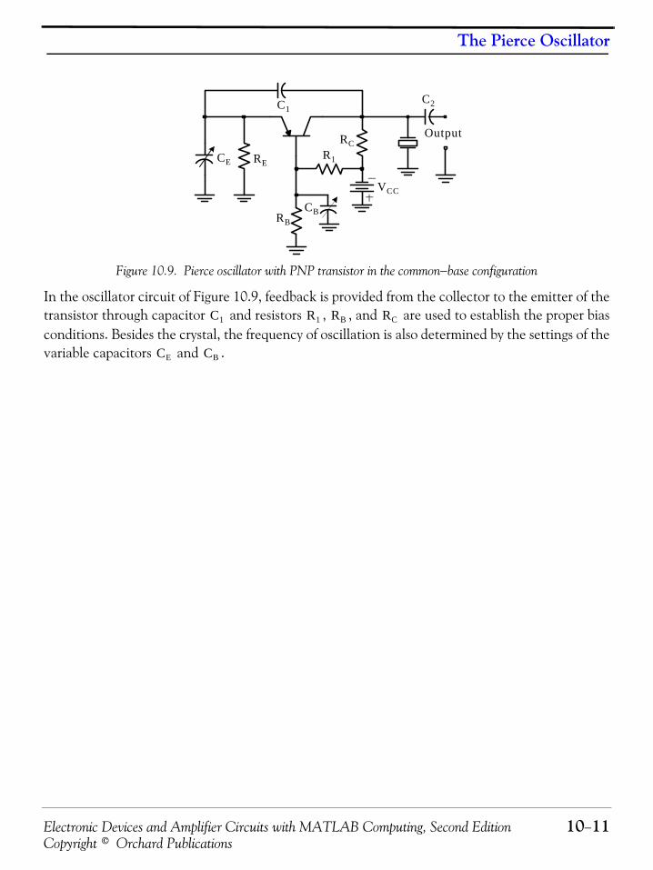
Electronic Devices and Amplifier Circuits with MATLAB Computing, Second Edition 10−11Copyright © Orchard Publications
The Pierce Oscillator
Figure 10.9. Pierce oscillator with PNP transistor in the common−base configuration
In the oscillator circuit of Figure 10.9, feedback is provided from the collector to the emitter of thetransistor through capacitor and resistors , , and are used to establish the proper biasconditions. Besides the crystal, the frequency of oscillation is also determined by the settings of thevariable capacitors and .
C1C2
CE
CBRB
RER1
RC
VCC
Output
C1 R1 RB RC
CE CB
Sinusoidal Oscillators
10−12 Electronic Devices and Amplifier Circuits with MATLAB Computing, Second EditionCopyright © Orchard Publications
10.10 Summary• An oscillator may be defined as a class of wave generators that produce sinusoidal, square, tri-
angular, and sawtooth waveforms. An oscillator is essentially an amplifier circuit that providesits own input signal. In this chapter we discussed sinusoidal oscillators. Non−sinusoidal oscil-lators are known as relaxation oscillators.
• Many low−frequency oscillators use resistors and capacitors to form their frequency−deter-mining networks and are referred to as RC oscillators. These are used in the audio−frequencyrange. Other types of employ inductors and capacitors for its frequency−determining network.These are known as the LC oscillators and use tank circuits, are commonly used for the higherradio frequencies.
• A third type of sinusoidal oscillator is the crystal−controlled oscillator. The crystal−controlledoscillator provides excellent frequency stability and is used from the middle of the audio rangethrough the radio frequency range.
• An oscillator must provide amplification where the amplification of signal power occurs fromthe input to the output of the oscillator and a portion of the output is fed back to the input tosustain a constant input.
• In an oscillator circuit the positive feedback must be large enough to compensate for circuitlosses so that oscillations will be sustained. Moreover, a practical oscillator must oscillate at apredetermined frequency and thus the oscillator must include a frequency−determiningdevice which essentially is a band−pass filter allowing only the desired frequency to pass.
• The output of the oscillator contains only a single sinusoidal frequency.
• In an RC oscillator the frequency of oscillations is determined by the values of resistance andcapacitance in the three sections. Variable resistors and capacitors are usually employed toprovide tuning in the feedback network for variations in phase shift. For an RC phase−shiftoscillator, the amplifier is biased for Class A operation to minimize distortion of the signal.
• In an RC phase−shift oscillator the frequency of oscillation (resonant frequency) can beapproximated from the relation
where is the number of RC sections.
• In an LC oscillator the sinusoidal signal is generated by the action of an inductor and a capac-itor. The feedback signal is coupled from the LC tank of the oscillator circuit by using a ticklercoil or a coil pair.
• In an Armstrong oscillator, the feedback is provided through a tickler coil.
• In a Hartley oscillator the feedback is provided through a coil pair.
ω01
RC n---------------=
n

Electronic Devices and Amplifier Circuits with MATLAB Computing, Second Edition 10−13Copyright © Orchard Publications
Summary
• In a Colpitts oscillator the feedback is provided through a capacitor pair.
• The Colpitts oscillator provides better frequency stability than the Armstrong and Hartleyoscillators. Moreover, the Colpitts oscillator is easier to tune and thus can be used for a widerange of frequencies.
• In crystal oscillators the frequency determining element is a quartz crystal. Because of theinherent characteristics of the quartz crystal the crystal oscillator may be held to extreme accu-racy of frequency stability. The frequency depends almost entirely on the thickness where thethinner the thickness, the higher the frequency of oscillation. However, the power obtainable islimited by the heat the crystal will withstand without fracturing.
• Crystal oscillators are used in applications where frequency accuracy and stability ar of utmostimportance such as broadcast transmitters and radar. The frequency stability of crystal−con-trolled oscillators depends on the quality factor Q. Besides the quartz crystal oscillators, otherprecision oscillators are constructed with cesium or rubidium.
• The Pierce oscillator is a modified Colpitts oscillator that uses a crystal as a parallel−resonantcircuit, and for this reason is often referred to as crystal−controlled Pierce oscillator.
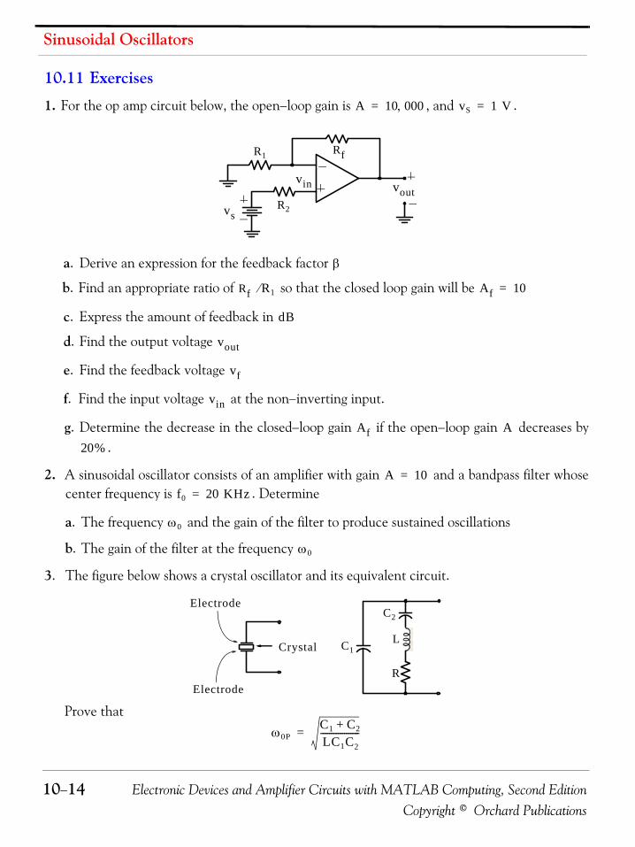
Sinusoidal Oscillators
10−14 Electronic Devices and Amplifier Circuits with MATLAB Computing, Second EditionCopyright © Orchard Publications
10.11 Exercises
1. For the op amp circuit below, the open−loop gain is , and .
a. Derive an expression for the feedback factor
b. Find an appropriate ratio of so that the closed loop gain will be
c. Express the amount of feedback in
d. Find the output voltage
e. Find the feedback voltage
f. Find the input voltage at the non−inverting input.
g. Determine the decrease in the closed−loop gain if the open−loop gain decreases by.
2. A sinusoidal oscillator consists of an amplifier with gain and a bandpass filter whosecenter frequency is . Determine
a. The frequency and the gain of the filter to produce sustained oscillations
b. The gain of the filter at the frequency
3. The figure below shows a crystal oscillator and its equivalent circuit.
Prove that
A 10 000,= vS 1 V=
RfR1
R2vs
voutvin
β
Rf R1⁄ Af 10=
dB
vout
vf
vin
Af A20%
A 10=
f0 20 KHz=
ω0
ω0
Crystal
Electrode
Electrode
C1
C2
L
R
ω0PC1 C2+LC1C2------------------=

Electronic Devices and Amplifier Circuits with MATLAB Computing, Second Edition 10−15Copyright © Orchard Publications
Solutions to End−of−Chapter Exercises
10.12 Solutions to End−of−Chapter Exercises1.
a. The feedback factor is the portion of the output voltage which appears at theinverting input, and by the voltage division expression
and thus
(1)
b. From relation (10.4) and with and we find that
from which (2)
With (1) and (2) above
c. The amount of feedback is and in
RfR1
R2vs
voutvin
β vout
v −( )R1
Rf R1+------------------⎝ ⎠
⎛ ⎞ vout=
βR1
Rf R1+------------------=
A 104= Af 10=
AfA
1 βA+----------------- 10 104
1 104β+---------------------= = =
β 103 1–
104----------------- 0.0999= =
RF R1⁄ R1 R1⁄+R1 R1⁄
--------------------------------------- 1β--- 1
0.0999---------------- 10.01= = =
1 Rf R1⁄+ 10.01=
RfR1------ 9.01=
1 βA+ dB
FeedbackdB 20 1 βA+( )log 20 1 0.0999 104×+( )log 60 dB= = =
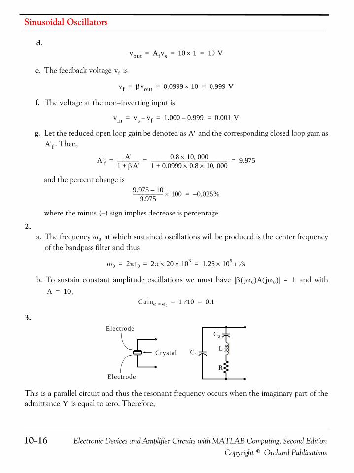
Sinusoidal Oscillators
10−16 Electronic Devices and Amplifier Circuits with MATLAB Computing, Second EditionCopyright © Orchard Publications
d.
e. The feedback voltage is
f. The voltage at the non−inverting input is
g. Let the reduced open loop gain be denoted as and the corresponding closed loop gain as. Then,
and the percent change is
where the minus (−) sign implies decrease is percentage.
2.a. The frequency at which sustained oscillations will be produced is the center frequency
of the bandpass filter and thus
b. To sustain constant amplitude oscillations we must have and with,
3.
This is a parallel circuit and thus the resonant frequency occurs when the imaginary part of theadmittance is equal to zero. Therefore,
vout Afvs 10 1× 10 V= = =
vf
vf βvout 0.0999 10× 0.999 V= = =
vin vs vf– 1.000 0.999– 0.001 V= = =
A'A'f
A'fA'
1 βA'+------------------ 0.8 10 000,×
1 0.0999 0.8 10 000,××+---------------------------------------------------------------- 9.975= = =
9.975 10–9.975
------------------------- 100× 0.025%–=
ω0
ω0 2πf0 2π 20 103×× 1.26 105× r s⁄= = =
β jω0( )A jω0( ) 1=
A 10=
Gainω ω0= 1 10⁄ 0.1= =
Crystal
Electrode
Electrode
C1
C2
L
R
Y

Electronic Devices and Amplifier Circuits with MATLAB Computing, Second Edition 10−17Copyright © Orchard Publications
Solutions to End−of−Chapter Exercises
Y jω0C11
jω0L 1 jω0C2⁄+----------------------------------------+ 0= =
jω0C1jω0C2
ω02LC2 1+–
-----------------------------+ 0=
jω0 C1C2
ω02LC2 1+–
-----------------------------+⎝ ⎠⎛ ⎞ 0=
C1C2
ω02LC2 1+–
-----------------------------+ 0=
C1C2
ω02LC2 1–
-------------------------=
ω02LC1C2 C1– C2=
ω0PC1 C2+LC1C2------------------=

Sinusoidal Oscillators
10−18 Electronic Devices and Amplifier Circuits with MATLAB Computing, Second EditionCopyright © Orchard Publications
NOTES:
Electronic Devices and Amplifier Circuits with MATLAB Computing, Second Edition A−1Copyright © Orchard Publications
Appendix A
Introduction to MATLAB®
his appendix serves as an introduction to the basic MATLAB commands and functions,procedures for naming and saving the user generated files, comment lines, access to MAT-LAB’s Editor / Debugger, finding the roots of a polynomial, and making plots. Several exam-
ples are provided with detailed explanations.
A.1 MATLAB® and Simulink®MATLAB and Simulink are products of The MathWorks,™ Inc. These are two outstanding soft-ware packages for scientific and engineering computations and are used in educational institu-tions and in industries including automotive, aerospace, electronics, telecommunications, andenvironmental applications. MATLAB enables us to solve many advanced numerical problemsrapidly and efficiently.
A.2 Command WindowTo distinguish the screen displays from the user commands, important terms, and MATLABfunctions, we will use the following conventions:
Click: Click the left button of the mouseCourier Font: Screen displaysHelvetica Font: User inputs at MATLAB’s command window prompt >> or EDU>>*
Helvetica Bold: MATLAB functions
Times Bold Italic: Important terms and facts, notes and file namesWhen we first start MATLAB, we see various help topics and other information. Initially, we areinterested in the command screen which can be selected from the Window drop menu. When thecommand screen, we see the prompt >> or EDU>>. This prompt is displayed also after executionof a command; MATLAB now waits for a new command from the user. It is highly recommendedthat we use the Editor/Debugger to write our program, save it, and return to the command screento execute the program as explained below.
To use the Editor/Debugger:
1. From the File menu on the toolbar, we choose New and click on M−File. This takes us to theEditor Window where we can type our script (list of statements) for a new file, or open a previ-ously saved file. We must save our program with a file name which starts with a letter. Impor-
* EDU>> is the MATLAB prompt in the Student Version
T
Appendix A Introduction to MATLAB®
A−2 Electronic Devices and Amplifier Circuits with MATLAB Computing, Second EditionCopyright © Orchard Publications
tant! MATLAB is case sensitive, that is, it distinguishes between upper− and lower−case let-ters. Thus, t and T are two different letters in MATLAB language. The files that we create aresaved with the file name we use and the extension .m; for example, myfile01.m. It is a goodpractice to save the script in a file name that is descriptive of our script content. For instance,if the script performs some matrix operations, we ought to name and save that file asmatrices01.m or any other similar name. We should also use a floppy disk or an external driveto backup our files.
2. Once the script is written and saved as an m−file, we may exit the Editor/Debugger window byclicking on Exit Editor/Debugger of the File menu. MATLAB then returns to the commandwindow.
3. To execute a program, we type the file name without the .m extension at the >> prompt;then, we press <enter> and observe the execution and the values obtained from it. If we havesaved our file in drive a or any other drive, we must make sure that it is added it to the desireddirectory in MATLAB’s search path. The MATLAB User’s Guide provides more informationon this topic.
Henceforth, it will be understood that each input command is typed after the >> prompt and fol-lowed by the <enter> key.
The command help matlab\iofun will display input/output information. To get help with otherMATLAB topics, we can type help followed by any topic from the displayed menu. For example,to get information on graphics, we type help matlab\graphics. The MATLAB User’s Guide con-tains numerous help topics.
To appreciate MATLAB’s capabilities, we type demo and we see the MATLAB Demos menu.We can do this periodically to become familiar with them. Whenever we want to return to thecommand window, we click on the Close button.
When we are done and want to leave MATLAB, we type quit or exit. But if we want to clear allprevious values, variables, and equations without exiting, we should use the command clear. Thiscommand erases everything; it is like exiting MATLAB and starting it again. The command clcclears the screen but MATLAB still remembers all values, variables and equations that we havealready used. In other words, if we want to clear all previously entered commands, leaving onlythe >> prompt on the upper left of the screen, we use the clc command.
All text after the % (percent) symbol is interpreted as a comment line by MATLAB, and thus it isignored during the execution of a program. A comment can be typed on the same line as the func-tion or command or as a separate line. For instance,
conv(p,q) % performs multiplication of polynomials p and q
% The next statement performs partial fraction expansion of p(x) / q(x)
are both correct.

Roots of Polynomials
Electronic Devices and Amplifier Circuits with MATLAB Computing, Second Edition A−3Copyright © Orchard Publications
One of the most powerful features of MATLAB is the ability to do computations involving com-plex numbers. We can use either , or to denote the imaginary part of a complex number, such as3-4i or 3-4j. For example, the statement
z=3−4j
displays
z = 3.0000−4.0000i
In the above example, a multiplication (*) sign between 4 and was not necessary because thecomplex number consists of numerical constants. However, if the imaginary part is a function, orvariable such as , we must use the multiplication sign, that is, we must type cos(x)*j orj*cos(x) for the imaginary part of the complex number.
A.3 Roots of Polynomials
In MATLAB, a polynomial is expressed as a row vector of the form . Theseare the coefficients of the polynomial in descending order. We must include terms whose coeffi-cients are zero.
We find the roots of any polynomial with the roots(p) function; p is a row vector containing thepolynomial coefficients in descending order.
Example A.1 Find the roots of the polynomial
Solution:The roots are found with the following two statements where we have denoted the polynomial asp1, and the roots as roots_ p1.
p1=[1 −10 35 −50 24] % Specify and display the coefficients of p1(x)
p1 = 1 -10 35 -50 24
roots_ p1=roots(p1) % Find the roots of p1(x)
roots_p1 =
4.0000 3.0000 2.0000 1.0000
i j
j
x( )cos
an an 1– … a2 a1 a0[ ]
p1 x( ) x4 10x3– 35x2 50x– 24+ +=

Appendix A Introduction to MATLAB®
A−4 Electronic Devices and Amplifier Circuits with MATLAB Computing, Second EditionCopyright © Orchard Publications
We observe that MATLAB displays the polynomial coefficients as a row vector, and the roots as acolumn vector.
Example A.2 Find the roots of the polynomial
Solution:There is no cube term; therefore, we must enter zero as its coefficient. The roots are found withthe statements below, where we have defined the polynomial as p2, and the roots of this polyno-mial as roots_ p2. The result indicates that this polynomial has three real roots, and two complexroots. Of course, complex roots always occur in complex conjugate* pairs.
p2=[1 −7 0 16 25 52]
p2 = 1 -7 0 16 25 52
roots_ p2=roots(p2)
roots_p2 = 6.5014 2.7428 -1.5711 -0.3366 + 1.3202i -0.3366 - 1.3202i
A.4 Polynomial Construction from Known RootsWe can compute the coefficients of a polynomial, from a given set of roots, with the poly(r) func-tion where r is a row vector containing the roots.
Example A.3
It is known that the roots of a polynomial are . Compute the coefficients of thispolynomial.
* By definition, the conjugate of a complex number is
p2 x( ) x5 7x4– 16x2 25x+ + 52+=
A a jb+= A∗ a jb–=
1 2 3 and 4, , ,

Polynomial Construction from Known Roots
Electronic Devices and Amplifier Circuits with MATLAB Computing, Second Edition A−5Copyright © Orchard Publications
Solution:
We first define a row vector, say , with the given roots as elements of this vector; then, we findthe coefficients with the poly(r) function as shown below.
r3=[1 2 3 4] % Specify the roots of the polynomial
r3 = 1 2 3 4
poly_r3=poly(r3) % Find the polynomial coefficients
poly_r3 = 1 -10 35 -50 24
We observe that these are the coefficients of the polynomial of Example A.1.
Example A.4
It is known that the roots of a polynomial are . Find the coeffi-cients of this polynomial.
Solution:
We form a row vector, say , with the given roots, and we find the polynomial coefficients withthe poly(r) function as shown below.
r4=[ −1 −2 −3 4+5j 4−5j ]
r4 = Columns 1 through 4 -1.0000 -2.0000 -3.0000 -4.0000+ 5.0000i Column 5 -4.0000- 5.0000i
poly_r4=poly(r4)
poly_r4 = 1 14 100 340 499 246
Therefore, the polynomial is
r3
p1 x( )
1 2 3 4 j5 and 4, j5–+,–,–,–
r4
p4 x( ) x5
14x4
100x3
340x2
499x 246+ + + + +=

Appendix A Introduction to MATLAB®
A−6 Electronic Devices and Amplifier Circuits with MATLAB Computing, Second EditionCopyright © Orchard Publications
A.5 Evaluation of a Polynomial at Specified Values
The polyval(p,x) function evaluates a polynomial at some specified value of the indepen-dent variable .
Example A.5 Evaluate the polynomial
(A.1)
at .
Solution:p5=[1 −3 0 5 −4 3 2]; % These are the coefficients of the given polynomial
% The semicolon (;) after the right bracket suppresses the % display of the row vector that contains the coefficients of p5.
%val_minus3=polyval(p5, −3) % Evaluate p5 at x=−3; no semicolon is used here
% because we want the answer to be displayed
val_minus3 = 1280
Other MATLAB functions used with polynomials are the following:
conv(a,b) − multiplies two polynomials a and b
[q,r]=deconv(c,d) −divides polynomial c by polynomial d and displays the quotient q andremainder r.
polyder(p) − produces the coefficients of the derivative of a polynomial p.
Example A.6 Let
and
Compute the product using the conv(a,b) function.
p x( )x
p5 x( ) x6 3x5– 5x3 4x2
– 3x 2+ + +=x 3–=
p1 x5 3x4– 5x2 7x 9+ + +=
p2 2x6 8x4– 4x2 10x 12+ + +=
p1 p2⋅

Evaluation of a Polynomial at Specified Values
Electronic Devices and Amplifier Circuits with MATLAB Computing, Second Edition A−7Copyright © Orchard Publications
Solution:p1=[1 −3 0 5 7 9]; % The coefficients of p1p2=[2 0 −8 0 4 10 12]; % The coefficients of p2p1p2=conv(p1,p2) % Multiply p1 by p2 to compute coefficients of the product p1p2
p1p2 =2 -6 -8 34 18 -24 -74 -88 78 166 174 108
Therefore,
Example A.7 Let
and
Compute the quotient using the [q,r]=deconv(c,d) function.
Solution:% It is permissible to write two or more statements in one line separated by semicolonsp3=[1 0 −3 0 5 7 9]; p4=[2 −8 0 0 4 10 12]; [q,r]=deconv(p3,p4)
q = 0.5000r = 0 4 -3 0 3 2 3
Therefore,
Example A.8 Let
Compute the derivative using the polyder(p) function.
p1 p2⋅ 2x11 6x10 8x9–– 34x8 18x7 24x6
–+ +=
74x5 88x4 78x3 166x2 174x 108+ + + +––
p3 x7 3x5– 5x3 7x 9+ + +=
p4 2x6 8x5– 4x2 10x 12+ + +=
p3 p4⁄
q 0.5= r 4x5 3x4– 3x2 2x 3+ + +=
p5 2x6 8x4– 4x2 10x 12+ + +=
ddx------p5

Appendix A Introduction to MATLAB®
A−8 Electronic Devices and Amplifier Circuits with MATLAB Computing, Second EditionCopyright © Orchard Publications
Solution:p5=[2 0 −8 0 4 10 12]; % The coefficients of p5der_p5=polyder(p5) % Compute the coefficients of the derivative of p5
der_p5 = 12 0 -32 0 8 10
Therefore,
A.6 Rational PolynomialsRational Polynomials are those which can be expressed in ratio form, that is, as
(A.2)
where some of the terms in the numerator and/or denominator may be zero. We can find the rootsof the numerator and denominator with the roots(p) function as before.
As noted in the comment line of Example A.7, we can write MATLAB statements in one line, ifwe separate them by commas or semicolons. Commas will display the results whereas semicolonswill suppress the display.
Example A.9 Let
Express the numerator and denominator in factored form, using the roots(p) function.
Solution:num=[1 −3 0 5 7 9]; den=[1 0 −4 0 2 5 6]; % Do not display num and den coefficientsroots_num=roots(num), roots_den=roots(den) % Display num and den roots
roots_num = 2.4186 + 1.0712i 2.4186 - 1.0712i -1.1633 -0.3370 + 0.9961i -0.3370 - 0.9961i
ddx------p5 12x5 32x3
– 4x2 8x 10+ + +=
R x( ) Num x( )Den x( )--------------------
bnxn bn 1– xn 1– bn 2– xn 2– … b1x b0+ + + + +
amxm am 1– xm 1– am 2– xm 2– … a1x a0+ + + + +------------------------------------------------------------------------------------------------------------------------= =
R x( )pnumpden------------ x5 3x4
– 5x2 7x 9+ + +
x6 4x4– 2x2 5x 6+ + +
---------------------------------------------------------= =
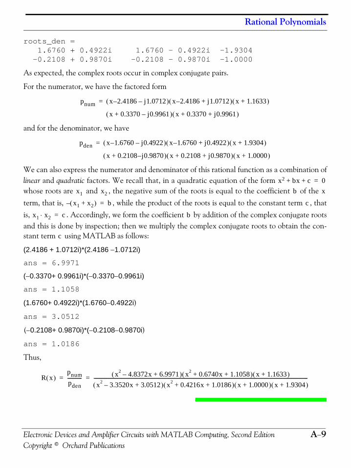
Rational Polynomials
Electronic Devices and Amplifier Circuits with MATLAB Computing, Second Edition A−9Copyright © Orchard Publications
roots_den = 1.6760 + 0.4922i 1.6760 - 0.4922i -1.9304 -0.2108 + 0.9870i -0.2108 - 0.9870i -1.0000
As expected, the complex roots occur in complex conjugate pairs.
For the numerator, we have the factored form
and for the denominator, we have
We can also express the numerator and denominator of this rational function as a combination oflinear and quadratic factors. We recall that, in a quadratic equation of the form whose roots are and , the negative sum of the roots is equal to the coefficient of the term, that is, , while the product of the roots is equal to the constant term , thatis, . Accordingly, we form the coefficient by addition of the complex conjugate rootsand this is done by inspection; then we multiply the complex conjugate roots to obtain the con-stant term using MATLAB as follows:
(2.4186 + 1.0712i)*(2.4186 −1.0712i)
ans = 6.9971
(−0.3370+ 0.9961i)*(−0.3370−0.9961i)
ans = 1.1058
(1.6760+ 0.4922i)*(1.6760−0.4922i)
ans = 3.0512
(−0.2108+ 0.9870i)*(−0.2108−0.9870i)
ans = 1.0186
Thus,
pnum x 2.4186– j1.0712–( ) x 2.4186– j1.0712+( ) x 1.1633+( )=
x 0.3370 j0.9961–+( ) x 0.3370 j0.9961+ +( )
pden x 1.6760– j0.4922–( ) x 1.6760– j0.4922+( ) x 1.9304+( )=
x 0.2108 j– 0.9870+( ) x 0.2108 j0.9870+ +( ) x 1.0000+( )
x2 bx c+ + 0=
x1 x2 b x
x1 x2+( )– b= c
x1 x2⋅ c= b
c
R x( )pnumpden------------ x2 4.8372x– 6.9971+( ) x2 0.6740x 1.1058+ +( ) x 1.1633+( )
x2 3.3520x– 3.0512+( ) x2 0.4216x 1.0186+ +( ) x 1.0000+( ) x 1.9304+( )------------------------------------------------------------------------------------------------------------------------------------------------------------------------------------= =
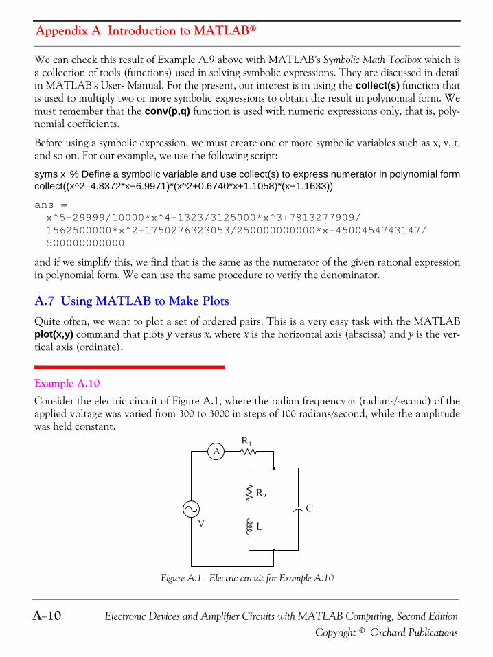
Appendix A Introduction to MATLAB®
A−10 Electronic Devices and Amplifier Circuits with MATLAB Computing, Second EditionCopyright © Orchard Publications
We can check this result of Example A.9 above with MATLAB’s Symbolic Math Toolbox which isa collection of tools (functions) used in solving symbolic expressions. They are discussed in detailin MATLAB’s Users Manual. For the present, our interest is in using the collect(s) function thatis used to multiply two or more symbolic expressions to obtain the result in polynomial form. Wemust remember that the conv(p,q) function is used with numeric expressions only, that is, poly-nomial coefficients.
Before using a symbolic expression, we must create one or more symbolic variables such as x, y, t,and so on. For our example, we use the following script:
syms x % Define a symbolic variable and use collect(s) to express numerator in polynomial formcollect((x^2−4.8372*x+6.9971)*(x^2+0.6740*x+1.1058)*(x+1.1633))
ans =x^5-29999/10000*x^4-1323/3125000*x^3+7813277909/1562500000*x^2+1750276323053/250000000000*x+4500454743147/500000000000
and if we simplify this, we find that is the same as the numerator of the given rational expressionin polynomial form. We can use the same procedure to verify the denominator.
A.7 Using MATLAB to Make PlotsQuite often, we want to plot a set of ordered pairs. This is a very easy task with the MATLABplot(x,y) command that plots y versus x, where x is the horizontal axis (abscissa) and y is the ver-tical axis (ordinate).
Example A.10 Consider the electric circuit of Figure A.1, where the radian frequency ω (radians/second) of theapplied voltage was varied from 300 to 3000 in steps of 100 radians/second, while the amplitudewas held constant.
Figure A.1. Electric circuit for Example A.10
A
V L
C
R2
R1
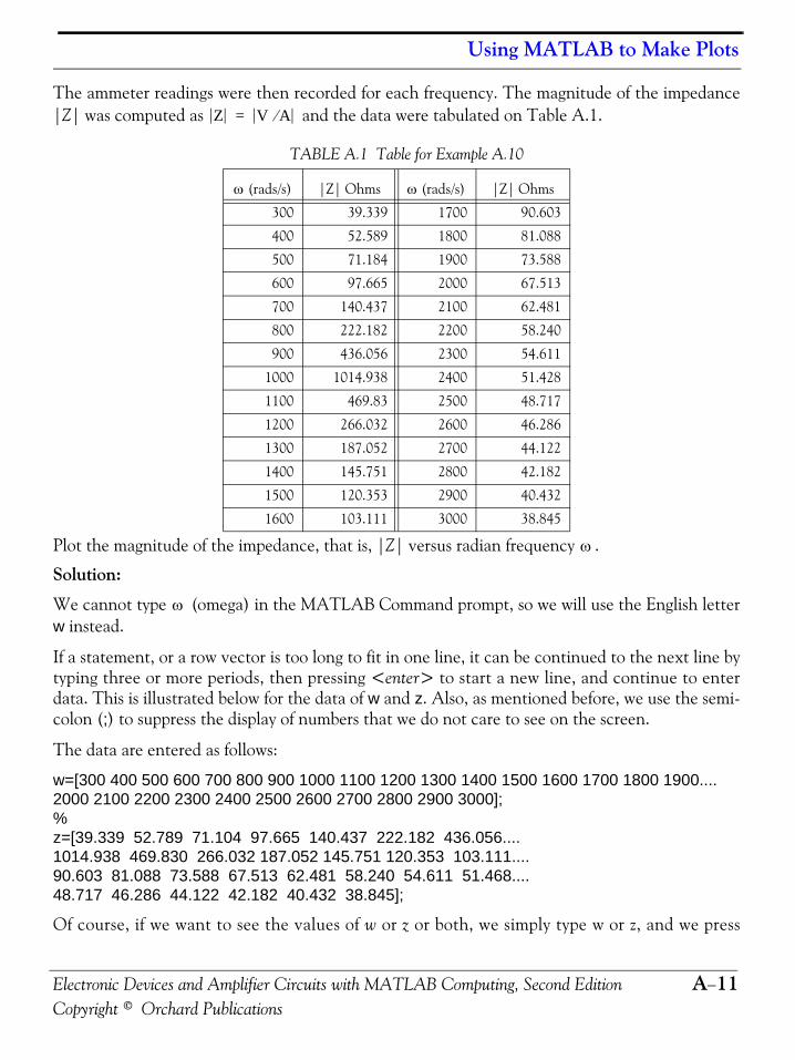
Using MATLAB to Make Plots
Electronic Devices and Amplifier Circuits with MATLAB Computing, Second Edition A−11Copyright © Orchard Publications
The ammeter readings were then recorded for each frequency. The magnitude of the impedance|Z| was computed as and the data were tabulated on Table A.1.
Plot the magnitude of the impedance, that is, |Z| versus radian frequency .
Solution:
We cannot type (omega) in the MATLAB Command prompt, so we will use the English letterw instead.
If a statement, or a row vector is too long to fit in one line, it can be continued to the next line bytyping three or more periods, then pressing <enter> to start a new line, and continue to enterdata. This is illustrated below for the data of w and z. Also, as mentioned before, we use the semi-colon (;) to suppress the display of numbers that we do not care to see on the screen.
The data are entered as follows:
w=[300 400 500 600 700 800 900 1000 1100 1200 1300 1400 1500 1600 1700 1800 1900....2000 2100 2200 2300 2400 2500 2600 2700 2800 2900 3000];%z=[39.339 52.789 71.104 97.665 140.437 222.182 436.056.... 1014.938 469.830 266.032 187.052 145.751 120.353 103.111.... 90.603 81.088 73.588 67.513 62.481 58.240 54.611 51.468.... 48.717 46.286 44.122 42.182 40.432 38.845];
Of course, if we want to see the values of w or z or both, we simply type w or z, and we press
TABLE A.1 Table for Example A.10
ω (rads/s) |Z| Ohms ω (rads/s) |Z| Ohms
300 39.339 1700 90.603
400 52.589 1800 81.088
500 71.184 1900 73.588
600 97.665 2000 67.513
700 140.437 2100 62.481
800 222.182 2200 58.240
900 436.056 2300 54.611
1000 1014.938 2400 51.428
1100 469.83 2500 48.717
1200 266.032 2600 46.286
1300 187.052 2700 44.122
1400 145.751 2800 42.182
1500 120.353 2900 40.432
1600 103.111 3000 38.845
Z V A⁄=
ω
ω
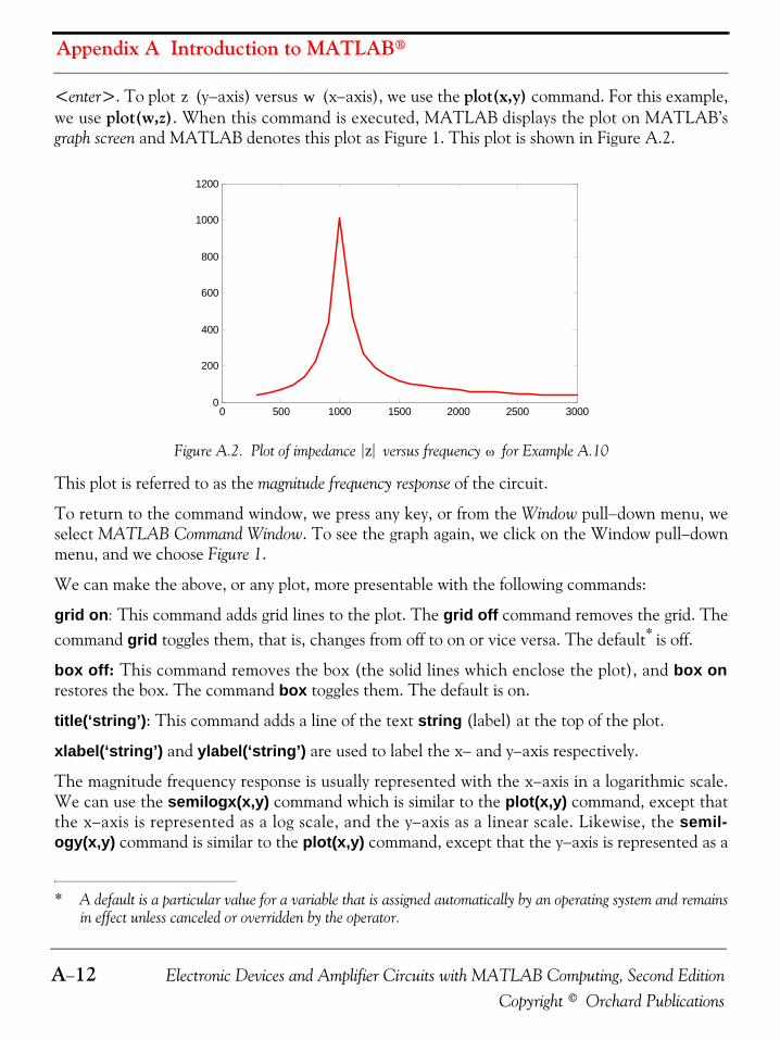
Appendix A Introduction to MATLAB®
A−12 Electronic Devices and Amplifier Circuits with MATLAB Computing, Second EditionCopyright © Orchard Publications
<enter>. To plot (y−axis) versus (x−axis), we use the plot(x,y) command. For this example,we use plot(w,z). When this command is executed, MATLAB displays the plot on MATLAB’sgraph screen and MATLAB denotes this plot as Figure 1. This plot is shown in Figure A.2.
Figure A.2. Plot of impedance versus frequency for Example A.10
This plot is referred to as the magnitude frequency response of the circuit.
To return to the command window, we press any key, or from the Window pull−down menu, weselect MATLAB Command Window. To see the graph again, we click on the Window pull−downmenu, and we choose Figure 1.
We can make the above, or any plot, more presentable with the following commands:
grid on: This command adds grid lines to the plot. The grid off command removes the grid. Thecommand grid toggles them, that is, changes from off to on or vice versa. The default* is off.
box off: This command removes the box (the solid lines which enclose the plot), and box onrestores the box. The command box toggles them. The default is on.
title(‘string’): This command adds a line of the text string (label) at the top of the plot.
xlabel(‘string’) and ylabel(‘string’) are used to label the x− and y−axis respectively.
The magnitude frequency response is usually represented with the x−axis in a logarithmic scale.We can use the semilogx(x,y) command which is similar to the plot(x,y) command, except thatthe x−axis is represented as a log scale, and the y−axis as a linear scale. Likewise, the semil-ogy(x,y) command is similar to the plot(x,y) command, except that the y−axis is represented as a
* A default is a particular value for a variable that is assigned automatically by an operating system and remainsin effect unless canceled or overridden by the operator.
z w
0 500 1000 1500 2000 2500 30000
200
400
600
800
1000
1200
z ω

Using MATLAB to Make Plots
Electronic Devices and Amplifier Circuits with MATLAB Computing, Second Edition A−13Copyright © Orchard Publications
log scale, and the x−axis as a linear scale. The loglog(x,y) command uses logarithmic scales forboth axes.
Throughout this text it will be understood that log is the common (base 10) logarithm, and ln isthe natural (base e) logarithm. We must remember, however, the function log(x) in MATLAB isthe natural logarithm, whereas the common logarithm is expressed as log10(x), and the logarithmto the base 2 as log2(x).
Let us now redraw the plot with the above options by adding the following statements:
semilogx(w,z); grid; % Replaces the plot(w,z) commandtitle('Magnitude of Impedance vs. Radian Frequency');xlabel('w in rads/sec'); ylabel('|Z| in Ohms')
After execution of these commands, the plot is as shown in Figure A.3.
If the y−axis represents power, voltage or current, the x−axis of the frequency response is moreoften shown in a logarithmic scale, and the y−axis in dB (decibels).
Figure A.3. Modified frequency response plot of Figure A.2.
To display the voltage in a dB scale on the y−axis, we add the relation dB=20*log10(v), and wereplace the semilogx(w,z) command with semilogx(w,dB).
The command gtext(‘string’)* switches to the current Figure Window, and displays a cross−hairthat can be moved around with the mouse. For instance, we can use the command gtext(‘Imped-ance |Z| versus Frequency’), and this will place a cross−hair in the Figure window. Then, using
* With the latest MATLAB Versions 6 and 7 (Student Editions 13 and 14), we can add text, lines and arrows directly intothe graph using the tools provided on the Figure Window. For advanced MATLAB graphics, please refer to The Math-Works Using MATLAB Graphics documentation.
102
103
104
0
200
400
600
800
1000
1200Magnitude of Impedance vs. Radian Frequency
w in rads/sec
|Z| i
n O
hms
v

Appendix A Introduction to MATLAB®
A−14 Electronic Devices and Amplifier Circuits with MATLAB Computing, Second EditionCopyright © Orchard Publications
the mouse, we can move the cross−hair to the position where we want our label to begin, and wepress <enter>.
The command text(x,y,’string’) is similar to gtext(‘string’). It places a label on a plot in somespecific location specified by x and y, and string is the label which we want to place at that loca-tion. We will illustrate its use with the following example which plots a 3−phase sinusoidal wave-form.
The first line of the script below has the form
linspace(first_value, last_value, number_of_values)
This function specifies the number of data points but not the increments between data points. Analternate function is
x=first: increment: last
and this specifies the increments between points but not the number of data points.
The script for the 3−phase plot is as follows:
x=linspace(0, 2*pi, 60); % pi is a built−in function in MATLAB;% we could have used x=0:0.02*pi:2*pi or x = (0: 0.02: 2)*pi instead;y=sin(x); u=sin(x+2*pi/3); v=sin(x+4*pi/3); plot(x,y,x,u,x,v); % The x−axis must be specified for each functiongrid on, box on, % turn grid and axes box ontext(0.75, 0.65, 'sin(x)'); text(2.85, 0.65, 'sin(x+2*pi/3)'); text(4.95, 0.65, 'sin(x+4*pi/3)')
These three waveforms are shown on the same plot of Figure A.4.
Figure A.4. Three−phase waveforms
0 1 2 3 4 5 6 7-1
-0.5
0
0.5
1
sin(x) sin(x+2*pi/3) sin(x+4*pi/3)

Using MATLAB to Make Plots
Electronic Devices and Amplifier Circuits with MATLAB Computing, Second Edition A−15Copyright © Orchard Publications
In our previous examples, we did not specify line styles, markers, and colors for our plots. How-ever, MATLAB allows us to specify various line types, plot symbols, and colors. These, or a com-bination of these, can be added with the plot(x,y,s) command, where s is a character string con-taining one or more characters shown on the three columns of Table A.2. MATLAB has nodefault color; it starts with blue and cycles through the first seven colors listed in Table A.2 foreach additional line in the plot. Also, there is no default marker; no markers are drawn unlessthey are selected. The default line is the solid line. But with the latest MATLAB versions, we canselect the line color, line width, and other options directly from the Figure Window.
For example, plot(x,y,'m*:') plots a magenta dotted line with a star at each data point, andplot(x,y,'rs') plots a red square at each data point, but does not draw any line because no line wasselected. If we want to connect the data points with a solid line, we must type plot(x,y,'rs−'). Foradditional information we can type help plot in MATLAB’s command screen.
The plots we have discussed thus far are two−dimensional, that is, they are drawn on two axes.MATLAB has also a three−dimensional (three−axes) capability and this is discussed next.
The plot3(x,y,z) command plots a line in 3−space through the points whose coordinates are theelements of x, y and z, where x, y and z are three vectors of the same length.
The general format is plot3(x1,y1,z1,s1,x2,y2,z2,s2,x3,y3,z3,s3,...) where xn, yn and zn are vectorsor matrices, and sn are strings specifying color, marker symbol, or line style. These strings are thesame as those of the two−dimensional plots.
TABLE A.2 Styles, colors, and markets used in MATLAB
Symbol Color Symbol Marker Symbol Line Style
b blue . point − solid line
g green o circle : dotted line
r red x x−mark −. dash−dot line
c cyan + plus −− dashed line
m magenta * star
y yellow s square
k black d diamond
w white ∨ triangle down
∧ triangle up
< triangle left
> triangle right
p pentagram
h hexagram
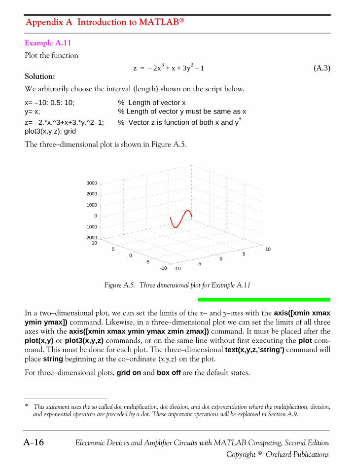
Appendix A Introduction to MATLAB®
A−16 Electronic Devices and Amplifier Circuits with MATLAB Computing, Second EditionCopyright © Orchard Publications
Example A.11 Plot the function
(A.3)Solution:We arbitrarily choose the interval (length) shown on the script below.
x= −10: 0.5: 10; % Length of vector x y= x; % Length of vector y must be same as x
z= −2.*x.^3+x+3.*y.^2−1; % Vector z is function of both x and y*
plot3(x,y,z); grid
The three−dimensional plot is shown in Figure A.5.
Figure A.5. Three dimensional plot for Example A.11
In a two−dimensional plot, we can set the limits of the x− and y−axes with the axis([xmin xmaxymin ymax]) command. Likewise, in a three−dimensional plot we can set the limits of all threeaxes with the axis([xmin xmax ymin ymax zmin zmax]) command. It must be placed after theplot(x,y) or plot3(x,y,z) commands, or on the same line without first executing the plot com-mand. This must be done for each plot. The three−dimensional text(x,y,z,’string’) command willplace string beginning at the co−ordinate (x,y,z) on the plot.
For three−dimensional plots, grid on and box off are the default states.
* This statement uses the so called dot multiplication, dot division, and dot exponentiation where the multiplication, division,and exponential operators are preceded by a dot. These important operations will be explained in Section A.9.
z 2x3– x 3y2 1–+ +=
-10-5
05
10
-10-5
05
10-2000
-1000
0
1000
2000
3000
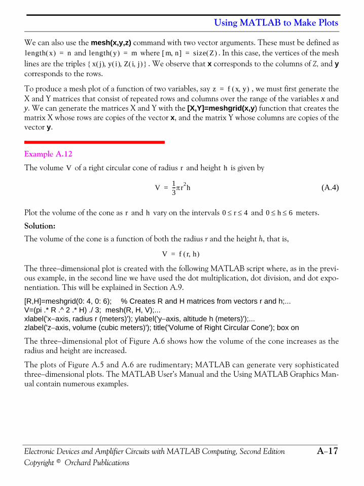
Using MATLAB to Make Plots
Electronic Devices and Amplifier Circuits with MATLAB Computing, Second Edition A−17Copyright © Orchard Publications
We can also use the mesh(x,y,z) command with two vector arguments. These must be defined as and where . In this case, the vertices of the mesh
lines are the triples . We observe that x corresponds to the columns of Z, and ycorresponds to the rows.
To produce a mesh plot of a function of two variables, say , we must first generate theX and Y matrices that consist of repeated rows and columns over the range of the variables x andy. We can generate the matrices X and Y with the [X,Y]=meshgrid(x,y) function that creates thematrix X whose rows are copies of the vector x, and the matrix Y whose columns are copies of thevector y.
Example A.12
The volume of a right circular cone of radius and height is given by
(A.4)
Plot the volume of the cone as and vary on the intervals and meters.
Solution:The volume of the cone is a function of both the radius r and the height h, that is,
The three−dimensional plot is created with the following MATLAB script where, as in the previ-ous example, in the second line we have used the dot multiplication, dot division, and dot expo-nentiation. This will be explained in Section A.9.
[R,H]=meshgrid(0: 4, 0: 6); % Creates R and H matrices from vectors r and h;...V=(pi .* R .^ 2 .* H) ./ 3; mesh(R, H, V);...xlabel('x−axis, radius r (meters)'); ylabel('y−axis, altitude h (meters)');...zlabel('z−axis, volume (cubic meters)'); title('Volume of Right Circular Cone'); box on
The three−dimensional plot of Figure A.6 shows how the volume of the cone increases as theradius and height are increased.
The plots of Figure A.5 and A.6 are rudimentary; MATLAB can generate very sophisticatedthree−dimensional plots. The MATLAB User’s Manual and the Using MATLAB Graphics Man-ual contain numerous examples.
length x( ) n= length y( ) m= m n,[ ] size Z( )=
x j( ) y i( ) Z i j,( ),,{ }
z f x y,( )=
V r h
V 13---πr2h=
r h 0 r 4≤ ≤ 0 h 6≤ ≤
V f r h,( )=
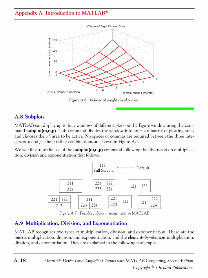
Appendix A Introduction to MATLAB®
A−18 Electronic Devices and Amplifier Circuits with MATLAB Computing, Second EditionCopyright © Orchard Publications
Figure A.6. Volume of a right circular cone.
A.8 SubplotsMATLAB can display up to four windows of different plots on the Figure window using the com-mand subplot(m,n,p). This command divides the window into an m × n matrix of plotting areasand chooses the pth area to be active. No spaces or commas are required between the three inte-gers m, n and p. The possible combinations are shown in Figure A.7.
We will illustrate the use of the subplot(m,n,p) command following the discussion on multiplica-tion, division and exponentiation that follows.
Figure A.7. Possible subplot arrangements in MATLAB
A.9 Multiplication, Division, and ExponentiationMATLAB recognizes two types of multiplication, division, and exponentiation. These are thematrix multiplication, division, and exponentiation, and the element−by−element multiplication,division, and exponentiation. They are explained in the following paragraphs.
01
23
4
0
2
4
60
50
100
150
x-axis, radius r (meters)
Volume of Right Circular Cone
y-axis, altitude h (meters)
z-ax
is,
volu
me
(cub
ic m
eter
s)
111Full Screen Default
211 212
221 222 223 224
121 122
221 222 212
211 223 224
221 223
122 121 222224
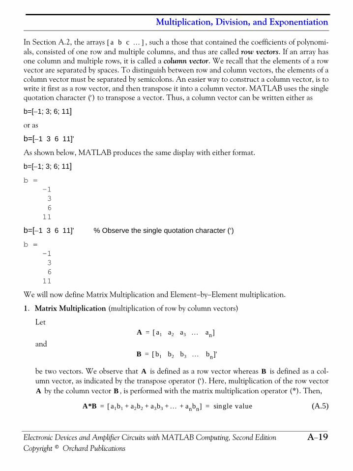
Multiplication, Division, and Exponentiation
Electronic Devices and Amplifier Circuits with MATLAB Computing, Second Edition A−19Copyright © Orchard Publications
In Section A.2, the arrays , such a those that contained the coefficients of polynomi-als, consisted of one row and multiple columns, and thus are called row vectors. If an array hasone column and multiple rows, it is called a column vector. We recall that the elements of a rowvector are separated by spaces. To distinguish between row and column vectors, the elements of acolumn vector must be separated by semicolons. An easier way to construct a column vector, is towrite it first as a row vector, and then transpose it into a column vector. MATLAB uses the singlequotation character (′) to transpose a vector. Thus, a column vector can be written either as
b=[−1; 3; 6; 11]
or as
b=[−1 3 6 11]'
As shown below, MATLAB produces the same display with either format.
b=[−1; 3; 6; 11]
b = -1 3 6 11
b=[−1 3 6 11]' % Observe the single quotation character (‘)
b = -1 3 6 11
We will now define Matrix Multiplication and Element−by−Element multiplication.
1. Matrix Multiplication (multiplication of row by column vectors)
Let
and
be two vectors. We observe that is defined as a row vector whereas is defined as a col-umn vector, as indicated by the transpose operator (′). Here, multiplication of the row vector
by the column vector , is performed with the matrix multiplication operator (*). Then,
(A.5)
a b c …[ ]
A a1 a2 a3 … an[ ]=
B b1 b2 b3 … bn[ ]'=
A B
A B
A*B a1b1 a2b2 a3b3 … anbn+ + + +[ ] gle valuesin= =
Appendix A Introduction to MATLAB®
A−20 Electronic Devices and Amplifier Circuits with MATLAB Computing, Second EditionCopyright © Orchard Publications
For example, if
and
the matrix multiplication produces the single value 68, that is,
and this is verified with the MATLAB script
A=[1 2 3 4 5]; B=[ −2 6 −3 8 7]'; A*B % Observe transpose operator (‘) in B
ans =
68
Now, let us suppose that both and are row vectors, and we attempt to perform a row−by−row multiplication with the following MATLAB statements.
A=[1 2 3 4 5]; B=[−2 6 −3 8 7]; A*B % No transpose operator (‘) here
When these statements are executed, MATLAB displays the following message:
??? Error using ==> *
Inner matrix dimensions must agree.
Here, because we have used the matrix multiplication operator (*) in A*B, MATLAB expectsvector to be a column vector, not a row vector. It recognizes that is a row vector, andwarns us that we cannot perform this multiplication using the matrix multiplication operator(*). Accordingly, we must perform this type of multiplication with a different operator. Thisoperator is defined below.
2. Element−by−Element Multiplication (multiplication of a row vector by another row vector)
Let
and
be two row vectors. Here, multiplication of the row vector by the row vector is per-formed with the dot multiplication operator (.*). There is no space between the dot and themultiplication symbol. Thus,
(A.6)
A 1 2 3 4 5[ ]=
B 2– 6 3– 8 7[ ]'=
A*B
A∗B 1 2–( ) 2 6 3 3–( ) 4 8 5 7×+×+×+×+× 68= =
A B
B B
C c1 c2 c3 … cn[ ]=
D d1 d2 d3 … dn[ ]=
C D
C.∗D c1d1 c2d2 c3d3 … cndn[ ]=
Multiplication, Division, and Exponentiation
Electronic Devices and Amplifier Circuits with MATLAB Computing, Second Edition A−21Copyright © Orchard Publications
This product is another row vector with the same number of elements, as the elements of and .
As an example, let
and
Dot multiplication of these two row vectors produce the following result.
Check with MATLAB:
C=[1 2 3 4 5]; % Vectors C and D must haveD=[−2 6 −3 8 7]; % same number of elementsC.*D % We observe that this is a dot multiplication
ans = -2 12 -9 32 35
Similarly, the division (/) and exponentiation (^) operators, are used for matrix division andexponentiation, whereas dot division (./) and dot exponentiation (.^) are used for element−by−element division and exponentiation, as illustrated in Examples A.11 and A.12 above.
We must remember that no space is allowed between the dot (.) and the multiplication, divi-sion, and exponentiation operators.
Note: A dot (.) is never required with the plus (+) and minus (−) operators.
Example A.13 Write the MATLAB script that produces a simple plot for the waveform defined as
(A.7)
in the seconds interval.
Solution:The MATLAB script for this example is as follows:
t=0: 0.01: 5; % Define t−axis in 0.01 incrementsy=3 .* exp(−4 .* t) .* cos(5 .* t)−2 .* exp(−3 .* t) .* sin(2 .* t) + t .^2 ./ (t+1);plot(t,y); grid; xlabel('t'); ylabel('y=f(t)'); title('Plot for Example A.13')
The plot for this example is shown in Figure A.8.
CD
C 1 2 3 4 5[ ]=
D 2– 6 3– 8 7[ ]=
C.∗D 1 2–( )× 2 6× 3 3–( )× 4 8 5 7×× 2– 12 9– 32 35= =
y f t( ) 3e 4t– 5tcos 2e 3t– 2tsin– t2
t 1+-----------+= =
0 t 5≤ ≤
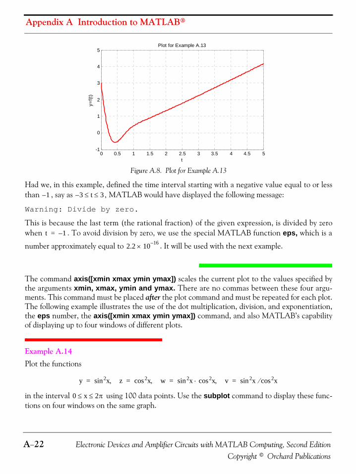
Appendix A Introduction to MATLAB®
A−22 Electronic Devices and Amplifier Circuits with MATLAB Computing, Second EditionCopyright © Orchard Publications
Figure A.8. Plot for Example A.13
Had we, in this example, defined the time interval starting with a negative value equal to or lessthan , say as , MATLAB would have displayed the following message:
Warning: Divide by zero.
This is because the last term (the rational fraction) of the given expression, is divided by zerowhen . To avoid division by zero, we use the special MATLAB function eps, which is a
number approximately equal to . It will be used with the next example.
The command axis([xmin xmax ymin ymax]) scales the current plot to the values specified bythe arguments xmin, xmax, ymin and ymax. There are no commas between these four argu-ments. This command must be placed after the plot command and must be repeated for each plot.The following example illustrates the use of the dot multiplication, division, and exponentiation,the eps number, the axis([xmin xmax ymin ymax]) command, and also MATLAB’s capabilityof displaying up to four windows of different plots.
Example A.14 Plot the functions
in the interval using 100 data points. Use the subplot command to display these func-tions on four windows on the same graph.
0 0.5 1 1.5 2 2.5 3 3.5 4 4.5 5-1
0
1
2
3
4
5
t
y=f(
t)
Plot for Example A.13
1– 3 t 3≤ ≤–
t 1–=
2.2 10 16–×
y x2sin z, x2cos w, x2sin x2cos⋅ v, x2sin x2cos⁄= = = =
0 x 2π≤ ≤
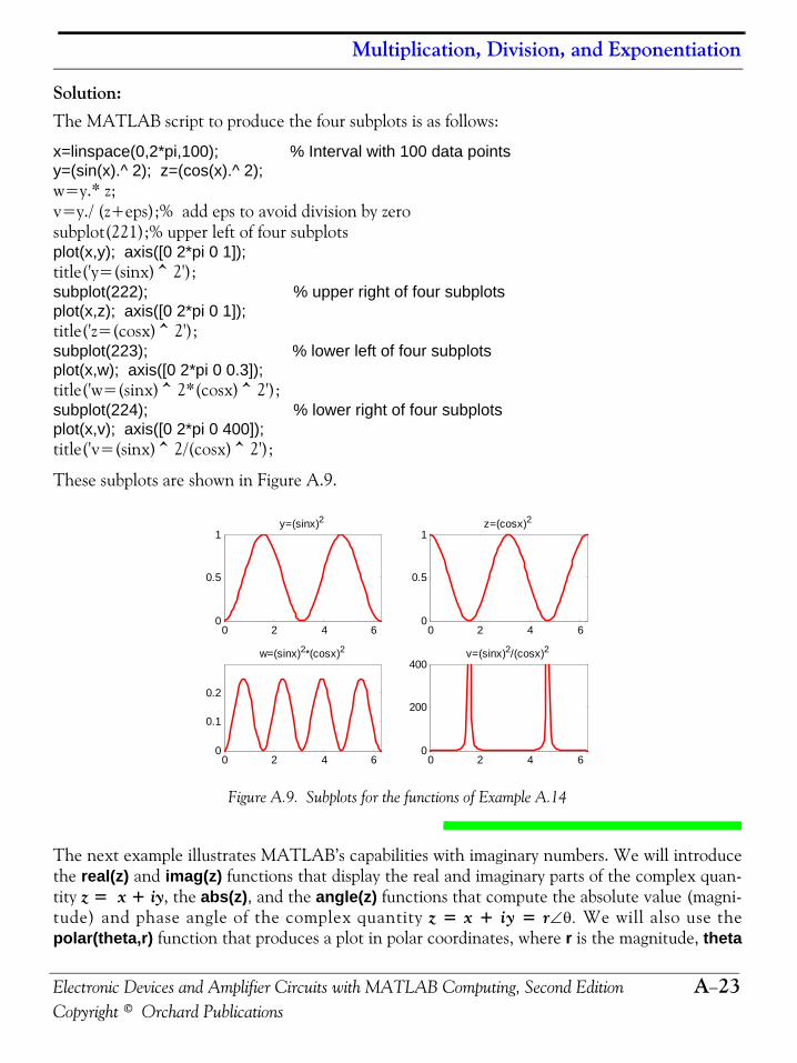
Multiplication, Division, and Exponentiation
Electronic Devices and Amplifier Circuits with MATLAB Computing, Second Edition A−23Copyright © Orchard Publications
Solution:The MATLAB script to produce the four subplots is as follows:
x=linspace(0,2*pi,100); % Interval with 100 data pointsy=(sin(x).^ 2); z=(cos(x).^ 2); w=y.* z;v=y./ (z+eps);% add eps to avoid division by zerosubplot(221);% upper left of four subplotsplot(x,y); axis([0 2*pi 0 1]);title('y=(sinx)^2');subplot(222); % upper right of four subplotsplot(x,z); axis([0 2*pi 0 1]); title('z=(cosx)^2');subplot(223); % lower left of four subplotsplot(x,w); axis([0 2*pi 0 0.3]);title('w=(sinx)^2*(cosx)^2');subplot(224); % lower right of four subplotsplot(x,v); axis([0 2*pi 0 400]);title('v=(sinx)^2/(cosx)^2');
These subplots are shown in Figure A.9.
Figure A.9. Subplots for the functions of Example A.14
The next example illustrates MATLAB’s capabilities with imaginary numbers. We will introducethe real(z) and imag(z) functions that display the real and imaginary parts of the complex quan-tity z = x + iy, the abs(z), and the angle(z) functions that compute the absolute value (magni-tude) and phase angle of the complex quantity z = x + iy = r∠θ. We will also use thepolar(theta,r) function that produces a plot in polar coordinates, where r is the magnitude, theta
0 2 4 60
0.5
1y=(sinx)2
0 2 4 60
0.5
1z=(cosx)2
0 2 4 60
0.1
0.2
w=(sinx)2*(cosx)2
0 2 4 60
200
400v=(sinx)2/(cosx)2
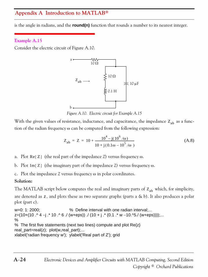
Appendix A Introduction to MATLAB®
A−24 Electronic Devices and Amplifier Circuits with MATLAB Computing, Second EditionCopyright © Orchard Publications
is the angle in radians, and the round(n) function that rounds a number to its nearest integer.
Example A.15 Consider the electric circuit of Figure A.10.
Figure A.10. Electric circuit for Example A.15
With the given values of resistance, inductance, and capacitance, the impedance as a func-tion of the radian frequency ω can be computed from the following expression:
(A.8)
a. Plot (the real part of the impedance Z) versus frequency ω.
b. Plot (the imaginary part of the impedance Z) versus frequency ω.
c. Plot the impedance Z versus frequency ω in polar coordinates.
Solution:
The MATLAB script below computes the real and imaginary parts of which, for simplicity,
are denoted as , and plots these as two separate graphs (parts a & b). It also produces a polarplot (part c).
w=0: 1: 2000; % Define interval with one radian interval;...z=(10+(10 .^ 4 −j .* 10 .^ 6 ./ (w+eps)) ./ (10 + j .* (0.1 .* w −10.^5./ (w+eps))));...%% The first five statements (next two lines) compute and plot Re{z}real_part=real(z); plot(w,real_part);...xlabel('radian frequency w'); ylabel('Real part of Z'); grid
a
b
10 Ω
10 Ω
0.1 H
10 μFZab
Zab
Zab Z 10 104 j 106 ω⁄( )–
10 j 0.1ω 105 ω⁄ –( )+--------------------------------------------------------+= =
Re Z{ }
Im Z{ }
Zab
z
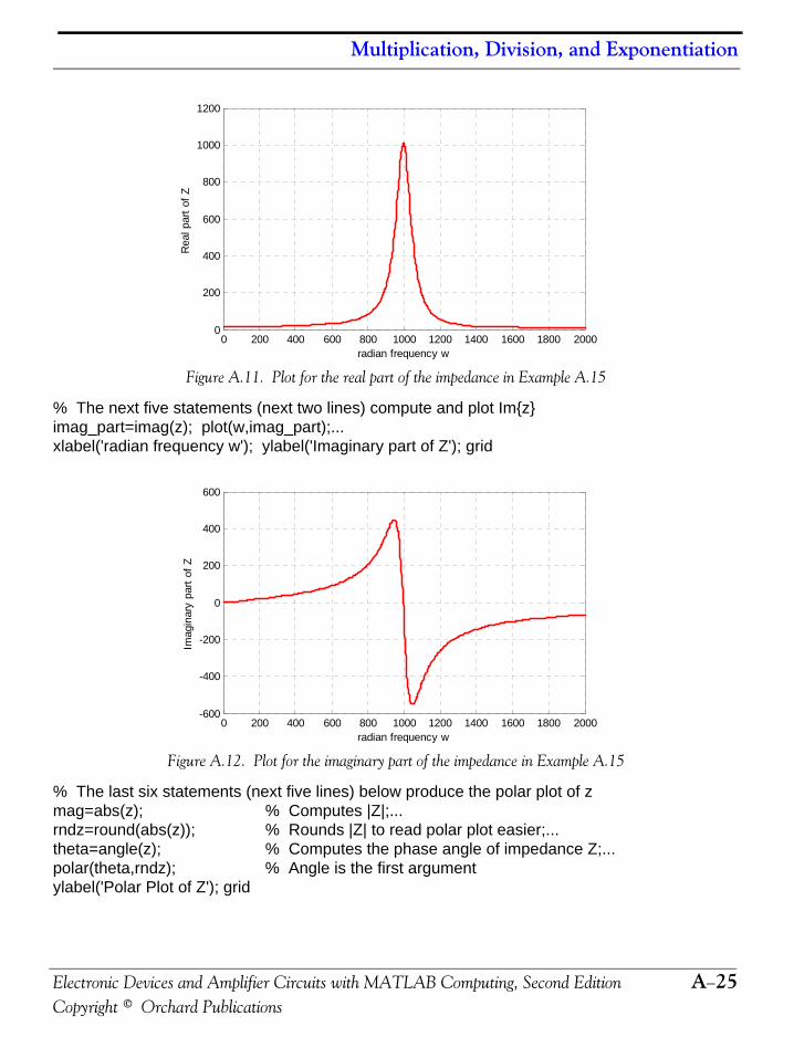
Multiplication, Division, and Exponentiation
Electronic Devices and Amplifier Circuits with MATLAB Computing, Second Edition A−25Copyright © Orchard Publications
Figure A.11. Plot for the real part of the impedance in Example A.15
% The next five statements (next two lines) compute and plot Im{z}imag_part=imag(z); plot(w,imag_part);...xlabel('radian frequency w'); ylabel('Imaginary part of Z'); grid
Figure A.12. Plot for the imaginary part of the impedance in Example A.15
% The last six statements (next five lines) below produce the polar plot of zmag=abs(z); % Computes |Z|;...rndz=round(abs(z)); % Rounds |Z| to read polar plot easier;...theta=angle(z); % Computes the phase angle of impedance Z;...polar(theta,rndz); % Angle is the first argumentylabel('Polar Plot of Z'); grid
0 200 400 600 800 1000 1200 1400 1600 1800 20000
200
400
600
800
1000
1200
radian frequency w
Rea
l par
t of
Z
0 200 400 600 800 1000 1200 1400 1600 1800 2000-600
-400
-200
0
200
400
600
radian frequency w
Imag
inar
y pa
rt o
f Z
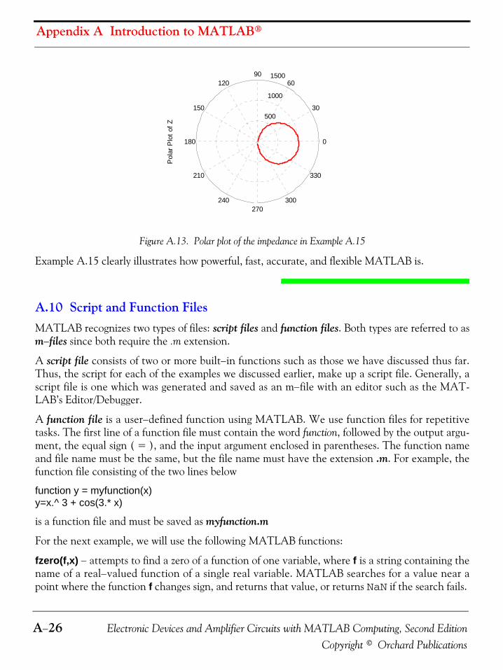
Appendix A Introduction to MATLAB®
A−26 Electronic Devices and Amplifier Circuits with MATLAB Computing, Second EditionCopyright © Orchard Publications
Figure A.13. Polar plot of the impedance in Example A.15
Example A.15 clearly illustrates how powerful, fast, accurate, and flexible MATLAB is.
A.10 Script and Function FilesMATLAB recognizes two types of files: script files and function files. Both types are referred to asm−files since both require the .m extension.
A script file consists of two or more built−in functions such as those we have discussed thus far.Thus, the script for each of the examples we discussed earlier, make up a script file. Generally, ascript file is one which was generated and saved as an m−file with an editor such as the MAT-LAB’s Editor/Debugger.
A function file is a user−defined function using MATLAB. We use function files for repetitivetasks. The first line of a function file must contain the word function, followed by the output argu-ment, the equal sign ( = ), and the input argument enclosed in parentheses. The function nameand file name must be the same, but the file name must have the extension .m. For example, thefunction file consisting of the two lines below
function y = myfunction(x)y=x.^ 3 + cos(3.* x)
is a function file and must be saved as myfunction.m
For the next example, we will use the following MATLAB functions:
fzero(f,x) − attempts to find a zero of a function of one variable, where f is a string containing thename of a real−valued function of a single real variable. MATLAB searches for a value near apoint where the function f changes sign, and returns that value, or returns NaN if the search fails.
500
1000
1500
30
210
60
240
90
270
120
300
150
330
180 0
Pol
ar P
lot
of Z

Script and Function Files
Electronic Devices and Amplifier Circuits with MATLAB Computing, Second Edition A−27Copyright © Orchard Publications
Important: We must remember that we use roots(p) to find the roots of polynomials only, such asthose in Examples A.1 and A.2.
fplot(fcn,lims) − plots the function specified by the string fcn between the x−axis limits specifiedby lims = [xmin xmax]. Using lims = [xmin xmax ymin ymax] also controls the y−axis limits.The string fcn must be the name of an m−file function or a string with variable .
NaN (Not−a−Number) is not a function; it is MATLAB’s response to an undefined expressionsuch as , , or inability to produce a result as described on the next paragraph. We canavoid division by zero using the eps number, which we mentioned earlier.
Example A.16 Find the zeros, the minimum, and the maximum values of the function
(A.9)
in the interval
Solution:We first plot this function to observe the approximate zeros, maxima, and minima using the fol-lowing script.
x=−1.5: 0.01: 1.5;y=1./ ((x−0.1).^ 2 + 0.01) −1./ ((x−1.2).^ 2 + 0.04) −10;plot(x,y); grid
The plot is shown in Figure A.14.
Figure A.14. Plot for Example A.16 using the plot command
x
0 0⁄ ∞ ∞⁄
f x( ) 1x 0.1–( )2 0.01+
---------------------------------------- 1x 1.2–( )2 0.04+
----------------------------------------– 10–=
1.5 x 1.5≤ ≤–
-1.5 -1 -0.5 0 0.5 1 1.5-40
-20
0
20
40
60
80
100

Appendix A Introduction to MATLAB®
A−28 Electronic Devices and Amplifier Circuits with MATLAB Computing, Second EditionCopyright © Orchard Publications
The roots (zeros) of this function appear to be in the neighborhood of and . Themaximum occurs at approximately where, approximately, , and the minimum
occurs at approximately where, approximately, .
Next, we define and save f(x) as the funczero01.m function m−file with the following script:
function y=funczero01(x)% Finding the zeros of the function shown belowy=1/((x−0.1)^2+0.01)−1/((x−1.2)^2+0.04)−10;
To save this file, from the File drop menu on the Command Window, we choose New, and whenthe Editor Window appears, we type the script above and we save it as funczero01. MATLABappends the extension .m to it.
Now, we can use the fplot(fcn,lims) command to plot as follows:
fplot('funczero01', [−1.5 1.5]); grid
This plot is shown in Figure A.15. As expected, this plot is identical to the plot of Figure A.14which was obtained with the plot(x,y) command as shown in Figure A.14.
Figure A.15. Plot for Example A.16 using the fplot command
We will use the fzero(f,x) function to compute the roots of in Equation (A.9) more precisely.The MATLAB script below will accomplish this.
x1= fzero('funczero01', −0.2);x2= fzero('funczero01', 0.3);fprintf('The roots (zeros) of this function are r1= %3.4f', x1);fprintf(' and r2= %3.4f \n', x2)
x 0.2–= x 0.3=
x 0.1= ymax 90=
x 1.2= ymin 34–=
f x( )
-1.5 -1 -0.5 0 0.5 1 1.5-40
-20
0
20
40
60
80
100
f x( )
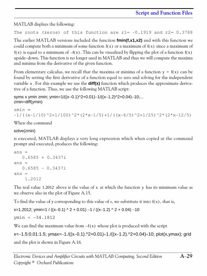
Script and Function Files
Electronic Devices and Amplifier Circuits with MATLAB Computing, Second Edition A−29Copyright © Orchard Publications
MATLAB displays the following:
The roots (zeros) of this function are r1= -0.1919 and r2= 0.3788
The earlier MATLAB versions included the function fmin(f,x1,x2) and with this function wecould compute both a minimum of some function or a maximum of since a maximum of
is equal to a minimum of . This can be visualized by flipping the plot of a function upside−down. This function is no longer used in MATLAB and thus we will compute the maximaand minima from the derivative of the given function.
From elementary calculus, we recall that the maxima or minima of a function can befound by setting the first derivative of a function equal to zero and solving for the independentvariable . For this example we use the diff(x) function which produces the approximate deriva-tive of a function. Thus, we use the following MATLAB script:
syms x ymin zmin; ymin=1/((x−0.1)^2+0.01)−1/((x−1.2)^2+0.04)−10;...zmin=diff(ymin)
zmin =-1/((x-1/10)^2+1/100)^2*(2*x-1/5)+1/((x-6/5)^2+1/25)^2*(2*x-12/5)
When the command
solve(zmin)
is executed, MATLAB displays a very long expression which when copied at the commandprompt and executed, produces the following:
ans = 0.6585 + 0.3437ians = 0.6585 - 0.3437ians = 1.2012
The real value above is the value of at which the function has its minimum value aswe observe also in the plot of Figure A.15.
To find the value of y corresponding to this value of x, we substitute it into , that is,
x=1.2012; ymin=1 / ((x−0.1) ^ 2 + 0.01) −1 / ((x−1.2) ^ 2 + 0.04) −10
ymin = -34.1812
We can find the maximum value from whose plot is produced with the script
x=−1.5:0.01:1.5; ymax=−1./((x−0.1).^2+0.01)+1./((x−1.2).^2+0.04)+10; plot(x,ymax); grid
and the plot is shown in Figure A.16.
f x( ) f x( )f x( ) f x( )– f x( )
y f x( )=
x
1.2012 x y
f x( )
f x( )–
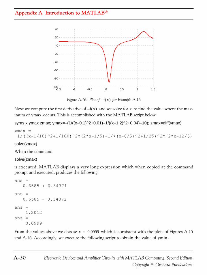
Appendix A Introduction to MATLAB®
A−30 Electronic Devices and Amplifier Circuits with MATLAB Computing, Second EditionCopyright © Orchard Publications
Figure A.16. Plot of for Example A.16
Next we compute the first derivative of and we solve for to find the value where the max-imum of occurs. This is accomplished with the MATLAB script below.
syms x ymax zmax; ymax=−(1/((x−0.1)^2+0.01)−1/((x−1.2)^2+0.04)−10); zmax=diff(ymax)
zmax = 1/((x-1/10)^2+1/100)^2*(2*x-1/5)-1/((x-6/5)^2+1/25)^2*(2*x-12/5)
solve(zmax)
When the command
solve(zmax)
is executed, MATLAB displays a very long expression which when copied at the commandprompt and executed, produces the following:
ans = 0.6585 + 0.3437i
ans = 0.6585 - 0.3437i
ans = 1.2012ans = 0.0999
From the values above we choose which is consistent with the plots of Figures A.15and A.16. Accordingly, we execute the following script to obtain the value of .
-1.5 -1 -0.5 0 0.5 1 1.5-100
-80
-60
-40
-20
0
20
40
f x( )–
f x( )– xymax
x 0.0999=
ymin

Display Formats
Electronic Devices and Amplifier Circuits with MATLAB Computing, Second Edition A−31Copyright © Orchard Publications
x=0.0999; % Using this value find the corresponding value of ymaxymax=1 / ((x−0.1) ^ 2 + 0.01) −1 / ((x−1.2) ^ 2 + 0.04) −10
ymax = 89.2000
A.11 Display FormatsMATLAB displays the results on the screen in integer format without decimals if the result is aninteger number, or in short floating point format with four decimals if it a fractional number. Theformat displayed has nothing to do with the accuracy in the computations. MATLAB performs allcomputations with accuracy up to 16 decimal places.
The output format can changed with the format command. The available MATLAB formats canbe displayed with the help format command as follows:
help format
FORMAT Set output format.All computations in MATLAB are done in double precision.FORMAT may be used to switch between different output display formatsas follows:
FORMAT Default. Same as SHORT.FORMAT SHORT Scaled fixed point format with 5 digits.FORMAT LONG Scaled fixed point format with 15 digits.FORMAT SHORT E Floating point format with 5 digits.FORMAT LONG E Floating point format with 15 digits.FORMAT SHORT G Best of fixed or floating point format with 5 digits.FORMAT LONG G Best of fixed or floating point format with 15 digits.FORMAT HEX Hexadecimal format.FORMAT + The symbols +, - and blank are printed for positive, negative,
and zero elements.Imaginary parts are ignored.FORMAT BANK Fixed format for dollars and cents.FORMAT RAT Approximation by ratio of small integers.
Spacing:
FORMAT COMPACT Suppress extra line-feeds.FORMAT LOOSE Puts the extra line-feeds back in.
Some examples with different format displays age given below.
format short 33.3335 Four decimal digits (default)format long 33.33333333333334 16 digitsformat short e 3.3333e+01 Four decimal digits plus exponentformat short g 33.333 Better of format short or format short eformat bank 33.33 two decimal digitsformat + only + or - or zero are printed
Appendix A Introduction to MATLAB®
A−32 Electronic Devices and Amplifier Circuits with MATLAB Computing, Second EditionCopyright © Orchard Publications
format rat 100/3 rational approximation
The disp(X) command displays the array X without printing the array name. If X is a string, thetext is displayed.
The fprintf(format,array) command displays and prints both text and arrays. It uses specifiers toindicate where and in which format the values would be displayed and printed. Thus, if %f isused, the values will be displayed and printed in fixed decimal format, and if %e is used, the val-ues will be displayed and printed in scientific notation format. With this command only the realpart of each parameter is processed.This appendix is just an introduction to MATLAB.* This outstanding software package consistsof many applications known as Toolboxes. The MATLAB Student Version contains just a few ofthese Toolboxes. Others can be bought directly from The MathWorks,™ Inc., as add−ons.
* For more MATLAB applications, please refer to Numerical Analysis Using MATLAB and Spreadsheets,ISBN 0−9709511−1−6.

Electronic Devices and Amplifier Circuits with MATLAB Computing, Second Edition B−1Copyright © Orchard Publications
Appendix B
Introduction to Simulink®
his appendix is a brief introduction to Simulink. This author feels that we can best intro-duce Simulink with a few examples. Some familiarity with MATLAB is essential in under-standing Simulink, and for this purpose, Appendix A is included as an introduction to
MATLAB.
B.1 Simulink and its Relation to MATLAB
The MATLAB® and Simulink® environments are integrated into one entity, and thus we cananalyze, simulate, and revise our models in either environment at any point. We invoke Simulinkfrom within MATLAB. We will introduce Simulink with a few illustrated examples.
Example B.1
For the circuit of Figure B.1, the initial conditions are , and . We will
compute .
Figure B.1. Circuit for Example B.1
For this example,
(B.1)
and by Kirchoff’s voltage law (KVL),
(B.2)
Substitution of (B.1) into (B.2) yields
T
iL 0−( ) 0= vc 0−( ) 0.5 V=
vc t( )
−
+R L
+−
C1 Ω
vs t( ) u0 t( )=
vC t( )i t( )
1 4⁄ H
4 3⁄ F
i iL iC CdvC
dt---------= = =
RiL LdiL
dt------- vC+ + u0 t( )=

Introduction to Simulink®
B−2 Electronic Devices and Amplifier Circuits with MATLAB Computing, Second EditionCopyright © Orchard Publications
(B.3)
Substituting the values of the circuit constants and rearranging we obtain:
(B.4)
(B.5)
To appreciate Simulink’s capabilities, for comparison, three different methods of obtaining thesolution are presented, and the solution using Simulink follows.
First Method − Assumed Solution
Equation (B.5) is a second−order, non−homogeneous differential equation with constant coeffi-cients, and thus the complete solution will consist of the sum of the forced response and the natu-ral response. It is obvious that the solution of this equation cannot be a constant since the deriva-tives of a constant are zero and thus the equation is not satisfied. Also, the solution cannotcontain sinusoidal functions (sine and cosine) since the derivatives of these are also sinusoids.
However, decaying exponentials of the form where k and a are constants, are possible candi-dates since their derivatives have the same form but alternate in sign.
It can be shown* that if and where and are constants and and are theroots of the characteristic equation of the homogeneous part of the given differential equation,
the natural response is the sum of the terms and . Therefore, the total solution willbe
(B.6)
The values of and are the roots of the characteristic equation
* Please refer to Circuit Analysis II with MATLAB Applications, ISBN 978−0−9709511−5−1, Appendix B fora thorough discussion.
RCdvC
dt--------- LC
d2vC
dt2----------- vC+ + u0 t( )=
13---d2vC
dt2----------- 4
3---dvC
dt--------- vC+ + u0 t( )=
d2vC
dt2----------- 4
dvC
dt--------- 3vC+ + 3u0 t( )=
d2vC
dt2----------- 4
dvC
dt--------- 3vC+ + 3= t 0>
ke at–
k1es1t–
k2es2t–
k1 k2 s1 s2
k1es1t–
k2es2t–
vc t( ) natural response forced response+ vcn t( ) vcf t( )+ k1es1t–
k2es2t–
vcf t( )+ += = =
s1 s2

Electronic Devices and Amplifier Circuits with MATLAB Computing, Second Edition B−3Copyright © Orchard Publications
Simulink and its Relation to MATLAB
(B.7)
Solution of (B.7) yields of and and with these values (B.6) is written as
(B.8)
The forced component is found from (B.5), i.e.,
(B.9)
Since the right side of (B.9) is a constant, the forced response will also be a constant and wedenote it as . By substitution into (B.9) we obtain
or (B.10)
Substitution of this value into (B.8), yields the total solution as
(B.11)
The constants and will be evaluated from the initial conditions. First, using and evaluating (B.11) at , we obtain
(B.12)
Also,
and
(B.13)
Next, we differentiate (B.11), we evaluate it at , and equate it with (B.13). Thus,
(B.14)
By equating the right sides of (B.13) and (B.14) we obtain
s2 4s 3+ + 0=
s1 1–= s2 3–=
vc t( ) k1e t– k2e 3– t vcf t( )+ +=
vcf t( )
d2vC
dt2----------- 4
dvC
dt--------- 3vC+ + 3= t 0>
vCf k3=
0 0 3k3+ + 3=
vCf k3 1= =
vC t( ) vCn t( ) vCf+= k1e t– k2e 3– t 1+ +=
k1 k2 vC 0( ) 0.5 V=
t 0=
vC 0( ) k1e0 k2e0 1+ + 0.5= =
k1 k2+ 0.5–=
iL iC CdvCdt
---------= = dvCdt
--------- iLC----=,
dvCdt
---------t 0=
iL 0( )C
------------ 0C---- 0= = =
t 0=
dvCdt
---------t 0=
k1– 3k2–=

Introduction to Simulink®
B−4 Electronic Devices and Amplifier Circuits with MATLAB Computing, Second EditionCopyright © Orchard Publications
(B.15)
Simultaneous solution of (B.12) and (B.15), gives and . By substitution into(B.8), we obtain the total solution as
(B.16)
Check with MATLAB:
syms t % Define symbolic variable ty0=−0.75*exp(−t)+0.25*exp(−3*t)+1; % The total solution y(t), for our example, vc(t)y1=diff(y0) % The first derivative of y(t)
y1 =3/4*exp(-t)-3/4*exp(-3*t)
y2=diff(y0,2) % The second derivative of y(t)
y2 =-3/4*exp(-t)+9/4*exp(-3*t)
y=y2+4*y1+3*y0 % Summation of y and its derivatives
y =3
Thus, the solution has been verified by MATLAB. Using the expression for in (B.16), wefind the expression for the current as
(B.17)
Second Method − Using the Laplace Transformation
The transformed circuit is shown in Figure B.2.
Figure B.2. Transformed Circuit for Example B.1
k1– 3k2– 0=
k1 0.75–= k2 0.25=
vC t( ) 0.75– e t– 0.25e 3– t 1+ +( )u0 t( )=
vC t( )
i iL= iC CdvCdt
---------- 43--- 3
4---e t– 3
4---– e 3t–
⎝ ⎠⎛ ⎞ e t– e 3t–– A= == =
−
+R L
+−
C 1
Vs s( ) 1 s⁄= VC s( )
I s( )
0.25s
3 4s⁄
+− VC 0( )
0.5 s⁄
Electronic Devices and Amplifier Circuits with MATLAB Computing, Second Edition B−5Copyright © Orchard Publications
Simulink and its Relation to MATLAB
By the voltage division* expression,
Using partial fraction expansion,† we let
(B.18)
and by substitution into (B.18)
Taking the Inverse Laplace transform‡ we find that
Third Method − Using State Variables
**
* For derivation of the voltage division and current division expressions, please refer to Circuit Analysis I withMATLAB Applications, ISBN 978−0−9709511−2−0.
† Partial fraction expansion is discussed in Chapter 3, Signals and Systems with MATLAB Computing and Sim-ulink Modeling, ISBN 978−1−934404−11−9
‡ For an introduction to Laplace Transform and Inverse Laplace Transform, please refer Chapters 2 and 3, Sig-nals and Systems with MATLAB Computing and Simulink Modeling, ISBN 978−1−934404−11−9
** Usually, in State−Space and State Variables Analysis, denotes any input. For distinction, we will denotethe Unit Step Function as . Please refer to Chapter 5, Signals and Systems with MATLAB Computingand Simulink Modeling, ISBN 978−1−934404−11−9
VC s( ) 3 4s⁄1 0.25s 3 4s⁄+ +( )
---------------------------------------------- 1s--- 0.5
s-------–⎝ ⎠
⎛ ⎞⋅ 0.5s
-------+= 1.5s s2 4s 3+ +( )--------------------------------- 0.5
s-------+ 0.5s2 2s 3+ +
s s 1+( ) s 3+( )------------------------------------= =
0.5s2 2s 3+ +s s 1+( ) s 3+( )------------------------------------
r1s----
r2s 1+( )
----------------r3
s 3+( )----------------+ +=
r10.5s2 2s 3+ +s 1+( ) s 3+( )
----------------------------------s 0=
1= =
r20.5s2 2s 3+ +
s s 3+( )----------------------------------
s 1–=
0.75–= =
r30.5s2 2s 3+ +
s s 1+( )----------------------------------
s 3–=
0.25= =
VC s( ) 0.5s2 2s 3+ +s s 1+( ) s 3+( )------------------------------------ 1
s--- 0.75–
s 1+( )---------------- 0.25
s 3+( )----------------+ += =
vC t( ) 1 0.75e t– 0.25e 3t–+–=
RiL LdiL
dt------- vC+ + u0 t( )=
u t( )u0 t( )

Introduction to Simulink®
B−6 Electronic Devices and Amplifier Circuits with MATLAB Computing, Second EditionCopyright © Orchard Publications
By substitution of given values and rearranging, we obtain
or
(B.19)
Next, we define the state variables and . Then,
* (B.20)
and
(B.21)
Also,
and thus,
or
(B.22)
Therefore, from (B.19), (B.20), and (B.22), we obtain the state equations
and in matrix form,
(B.23)
Solution† of (B.23) yields
* The notation (x dot) is often used to denote the first derivative of the function , that is, .
† The detailed solution of (B.23) is given in Chapter 5, Example 5.10, Page 5−23, Signals and Systems withMATLAB Computing and Simulink Modeling, ISBN 978−1−934404−11−9
14---diL
dt------- 1–( )iL vC– 1+=
diL
dt------- 4iL– 4vC– 4+=
x1 iL= x2 vC=
x· 1diL
dt-------=
x· x x· dx dt⁄=
x· 2dvC
dt---------=
iL CdvC
dt---------=
x1 iL CdvC
dt--------- Cx· 2
43---x· 2= = = =
x· 234---x1=
x· 1 4x1– 4x2– 4+=
x· 234--- x1=
x· 1
x· 2
4– 4–
3 4⁄ 0x1
x2
40
u0 t( )+=

Electronic Devices and Amplifier Circuits with MATLAB Computing, Second Edition B−7Copyright © Orchard Publications
Simulink and its Relation to MATLAB
Then,
(B.24)
and
(B.25)
Modeling the Differential Equation of Example B.1 with Simulink
To run Simulink, we must first invoke MATLAB. Make sure that Simulink is installed in your sys-tem. In the MATLAB Command prompt, we type:
simulink
Alternately, we can click on the Simulink icon shown in Figure B.3. It appears on the top bar onMATLAB’s Command prompt.
Figure B.3. The Simulink icon
Upon execution of the Simulink command, the Commonly Used Blocks appear as shown in Fig-ure B.4.
In Figure B.4, the left side is referred to as the Tree Pane and displays all Simulink librariesinstalled. The right side is referred to as the Contents Pane and displays the blocks that reside inthe library currently selected in the Tree Pane.
Let us express the differential equation of Example B.1 as
(B.26)
A block diagram representing relation (B.26) above is shown in Figure B.5. We will use Simulinkto draw a similar block diagram.*
* Henceforth, all Simulink block diagrams will be referred to as models.
x1
x2
e t– e– 3t–
1 0.75– e t– 0.25e 3t–+=
x1 iL e t– e– 3t–= =
x2 vC 1 0.75e– t– 0.25e 3t–+= =
d2vC
dt2----------- 4
dvC
dt--------- 3vC 3u0 t( )+––=

Introduction to Simulink®
B−8 Electronic Devices and Amplifier Circuits with MATLAB Computing, Second EditionCopyright © Orchard Publications
Figure B.4. The Simulink Library Browser
Figure B.5. Block diagram for equation (B.26)
To model the differential equation (B.26) using Simulink, we perform the following steps:
1. On the Simulink Library Browser, we click on the leftmost icon shown as a blank page on thetop title bar. A new model window named untitled will appear as shown in Figure B.6.
3u0 t( ) Σ dt∫ dt∫
−4
−3
d2vC
dt2----------- dvC
dt--------- vC
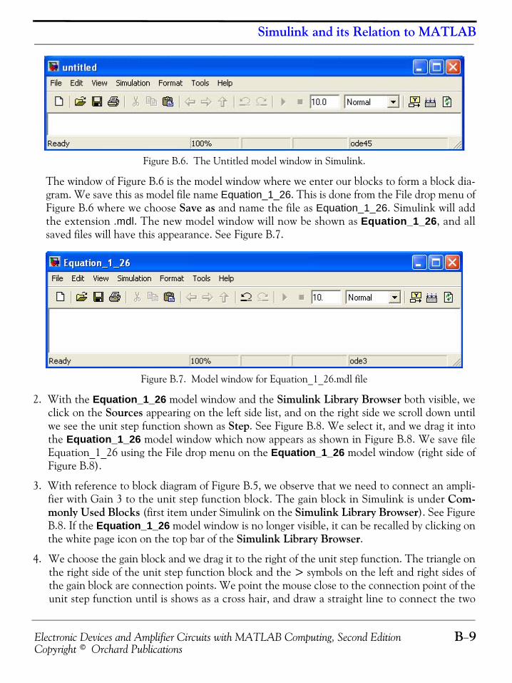
Electronic Devices and Amplifier Circuits with MATLAB Computing, Second Edition B−9Copyright © Orchard Publications
Simulink and its Relation to MATLAB
Figure B.6. The Untitled model window in Simulink.
The window of Figure B.6 is the model window where we enter our blocks to form a block dia-gram. We save this as model file name Equation_1_26. This is done from the File drop menu ofFigure B.6 where we choose Save as and name the file as Equation_1_26. Simulink will addthe extension .mdl. The new model window will now be shown as Equation_1_26, and allsaved files will have this appearance. See Figure B.7.
Figure B.7. Model window for Equation_1_26.mdl file
2. With the Equation_1_26 model window and the Simulink Library Browser both visible, weclick on the Sources appearing on the left side list, and on the right side we scroll down untilwe see the unit step function shown as Step. See Figure B.8. We select it, and we drag it intothe Equation_1_26 model window which now appears as shown in Figure B.8. We save fileEquation_1_26 using the File drop menu on the Equation_1_26 model window (right side ofFigure B.8).
3. With reference to block diagram of Figure B.5, we observe that we need to connect an ampli-fier with Gain 3 to the unit step function block. The gain block in Simulink is under Com-monly Used Blocks (first item under Simulink on the Simulink Library Browser). See FigureB.8. If the Equation_1_26 model window is no longer visible, it can be recalled by clicking onthe white page icon on the top bar of the Simulink Library Browser.
4. We choose the gain block and we drag it to the right of the unit step function. The triangle onthe right side of the unit step function block and the > symbols on the left and right sides ofthe gain block are connection points. We point the mouse close to the connection point of theunit step function until is shows as a cross hair, and draw a straight line to connect the two

Introduction to Simulink®
B−10 Electronic Devices and Amplifier Circuits with MATLAB Computing, Second EditionCopyright © Orchard Publications
blocks.* We double−click on the gain block and on the Function Block Parameters, wechange the gain from 1 to 3. See Figure B.9.
Figure B.8. Dragging the unit step function into File Equation_1_26
Figure B.9. File Equation_1_26 with added Step and Gain blocks
* An easy method to interconnect two Simulink blocks by clicking on the source block to select it, then hold downthe Ctrl key and left−click on the destination block.
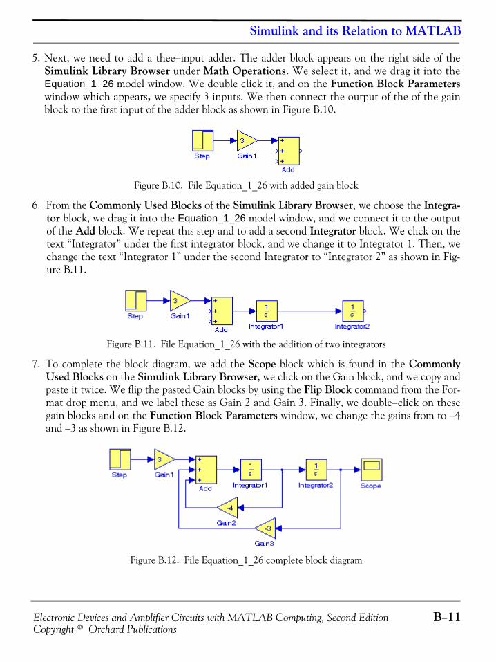
Electronic Devices and Amplifier Circuits with MATLAB Computing, Second Edition B−11Copyright © Orchard Publications
Simulink and its Relation to MATLAB
5. Next, we need to add a thee−input adder. The adder block appears on the right side of theSimulink Library Browser under Math Operations. We select it, and we drag it into theEquation_1_26 model window. We double click it, and on the Function Block Parameterswindow which appears, we specify 3 inputs. We then connect the output of the of the gainblock to the first input of the adder block as shown in Figure B.10.
Figure B.10. File Equation_1_26 with added gain block
6. From the Commonly Used Blocks of the Simulink Library Browser, we choose the Integra-tor block, we drag it into the Equation_1_26 model window, and we connect it to the outputof the Add block. We repeat this step and to add a second Integrator block. We click on thetext “Integrator” under the first integrator block, and we change it to Integrator 1. Then, wechange the text “Integrator 1” under the second Integrator to “Integrator 2” as shown in Fig-ure B.11.
Figure B.11. File Equation_1_26 with the addition of two integrators
7. To complete the block diagram, we add the Scope block which is found in the CommonlyUsed Blocks on the Simulink Library Browser, we click on the Gain block, and we copy andpaste it twice. We flip the pasted Gain blocks by using the Flip Block command from the For-mat drop menu, and we label these as Gain 2 and Gain 3. Finally, we double−click on thesegain blocks and on the Function Block Parameters window, we change the gains from to −4and −3 as shown in Figure B.12.
Figure B.12. File Equation_1_26 complete block diagram

Introduction to Simulink®
B−12 Electronic Devices and Amplifier Circuits with MATLAB Computing, Second EditionCopyright © Orchard Publications
8. The initial conditions , and are entered by dou-
ble clicking the Integrator blocks and entering the values for the first integrator, and forthe second integrator. We also need to specify the simulation time. This is done by specifyingthe simulation time to be seconds on the Configuration Parameters from the Simulationdrop menu. We can start the simulation on Start from the Simulation drop menu or by click-
ing on the icon.
9. To see the output waveform, we double click on the Scope block, and then clicking on the
Autoscale icon, we obtain the waveform shown in Figure B.13.
Figure B.13. The waveform for the function for Example B.1
Another easier method to obtain and display the output for Example B.1, is to use State−Space block from Continuous in the Simulink Library Browser, as shown in Figure B.14.
Figure B.14. Obtaining the function for Example B.1 with the State−Space block.
iL 0−( ) C dvC dt⁄( )t 0=
0= = vc 0−( ) 0.5 V=
0 0.5
10
vC t( )
vC t( )
vC t( )

Electronic Devices and Amplifier Circuits with MATLAB Computing, Second Edition B−13Copyright © Orchard Publications
Simulink and its Relation to MATLAB
The simout To Workspace block shown in Figure B.14 writes its input to the workspace. Thedata and variables created in the MATLAB Command window, reside in the MATLAB Work-space. This block writes its output to an array or structure that has the name specified by theblock's Variable name parameter. This gives us the ability to delete or modify selected variables.We issue the command who to see those variables. From Equation B.23, Page B−6,
The output equation is
or
We double−click on the State−Space block, and in the Functions Block Parameters window weenter the constants shown in Figure B.15.
Figure B.15. The Function block parameters for the State−Space block.
x· 1
x· 2
4– 4–
3 4⁄ 0x1
x2
40
u0 t( )+=
y Cx du+=
y 0 1[ ] x1
x2
0[ ]u+=
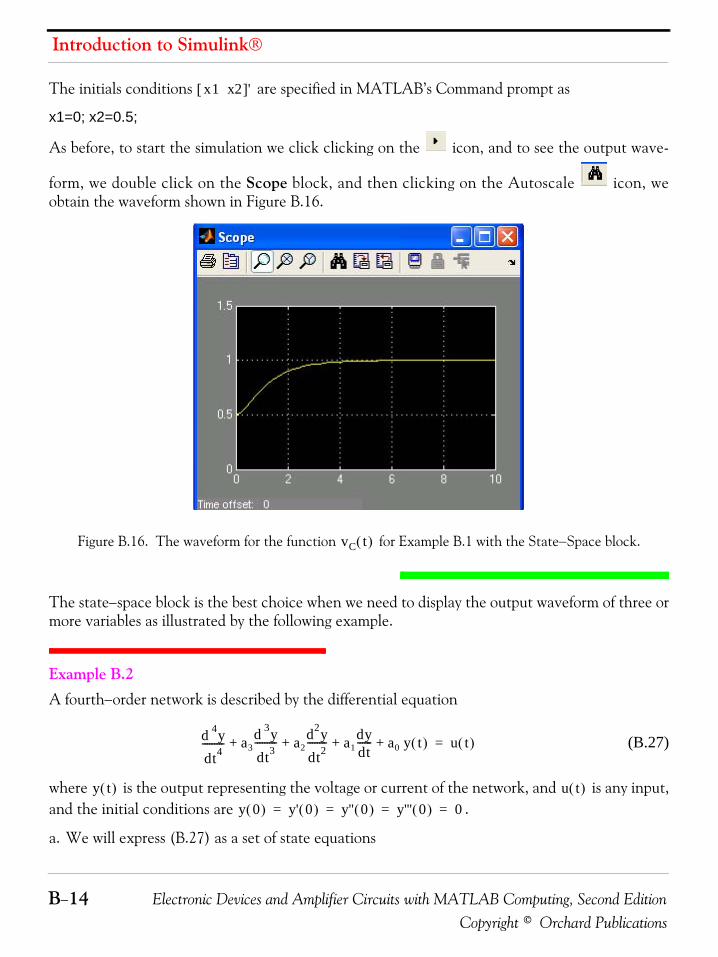
Introduction to Simulink®
B−14 Electronic Devices and Amplifier Circuits with MATLAB Computing, Second EditionCopyright © Orchard Publications
The initials conditions are specified in MATLAB’s Command prompt as
x1=0; x2=0.5;
As before, to start the simulation we click clicking on the icon, and to see the output wave-
form, we double click on the Scope block, and then clicking on the Autoscale icon, weobtain the waveform shown in Figure B.16.
Figure B.16. The waveform for the function for Example B.1 with the State−Space block.
The state−space block is the best choice when we need to display the output waveform of three ormore variables as illustrated by the following example.
Example B.2 A fourth−order network is described by the differential equation
(B.27)
where is the output representing the voltage or current of the network, and is any input,and the initial conditions are .
a. We will express (B.27) as a set of state equations
x1 x2[ ]'
vC t( )
d 4ydt4--------- a3
d 3ydt3--------- a2
d2ydt2-------- a1
dydt------ a0 y t( )+ + + + u t( )=
y t( ) u t( )y 0( ) y' 0( ) y'' 0( ) y''' 0( ) 0= = = =
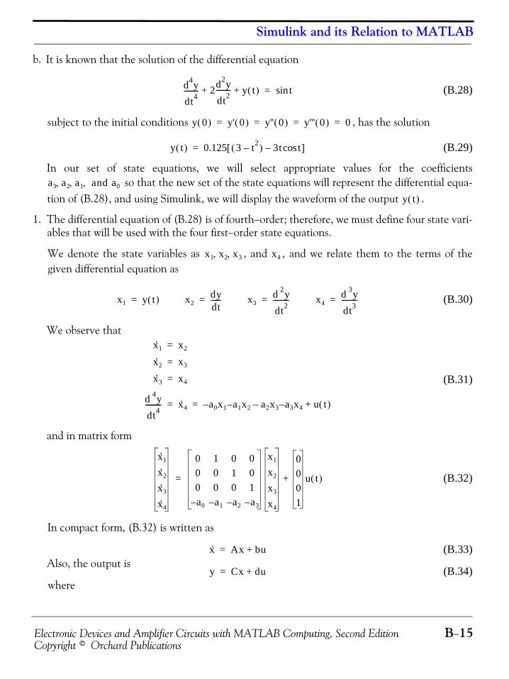
Electronic Devices and Amplifier Circuits with MATLAB Computing, Second Edition B−15Copyright © Orchard Publications
Simulink and its Relation to MATLAB
b. It is known that the solution of the differential equation
(B.28)
subject to the initial conditions , has the solution
(B.29)
In our set of state equations, we will select appropriate values for the coefficients so that the new set of the state equations will represent the differential equa-
tion of (B.28), and using Simulink, we will display the waveform of the output .
1. The differential equation of (B.28) is of fourth−order; therefore, we must define four state vari-ables that will be used with the four first−order state equations.
We denote the state variables as , and , and we relate them to the terms of thegiven differential equation as
(B.30)
We observe that
(B.31)
and in matrix form
(B.32)
In compact form, (B.32) is written as
(B.33)Also, the output is
(B.34)where
d4ydt4-------- 2d2y
dt2-------- y t( )+ + tsin=
y 0( ) y' 0( ) y'' 0( ) y''' 0( ) 0= = = =
y t( ) 0.125 3 t2–( ) 3t tcos–[ ]=
a3 a2 a1 and a0, , ,
y t( )
x1 x2 x3, , x4
x1 y t( )= x2dydt------= x3
d 2ydt2---------= x4
d 3ydt3---------=
x· 1 x2=
x· 2 x3=
x· 3 x4=
d 4ydt4--------- x· 4 a0x1– a1x2 a2x3–– a3x4– u t( )+= =
x· 1
x· 2
x· 3
x· 4
0 1 0 00 0 1 00 0 0 1a0– a1– a2– a3–
x1
x2
x3
x4
0001
u t( )+=
x· Ax bu+=
y Cx du+=

Introduction to Simulink®
B−16 Electronic Devices and Amplifier Circuits with MATLAB Computing, Second EditionCopyright © Orchard Publications
(B.35)
and since the output is defined as
relation (B.34) is expressed as
(B.36)
2. By inspection, the differential equation of (B.27) will be reduced to the differential equation of(B.28) if we let
and thus the differential equation of (B.28) can be expressed in state−space form as
(B.37)
where
(B.38)
Since the output is defined as
in matrix form it is expressed as
x·
x· 1
x· 2
x· 3
x· 4
= A
0 1 0 00 0 1 00 0 0 1a0– a1– a2– a3–
= x
x1
x2
x3
x4
= b
0001
and u,=, , , u t( )=
y t( ) x1=
y 1 0 0 0[ ]
x1
x2
x3
x4
⋅ 0[ ]u t( )+=
a3 0= a2 2= a1 0= a0 1= u t( ) tsin=
x· 1
x· 2
x· 3
x· 4
0 1 0 00 0 1 00 0 0 1a0– 0 2– 0
x1
x2
x3
x4
0001
tsin+=
x·
x· 1
x· 2
x· 3
x· 4
= A
0 1 0 00 0 1 00 0 0 1a0– 0 2– 0
= x
x1
x2
x3
x4
= b
0001
and u,=, , , tsin=
y t( ) x1=
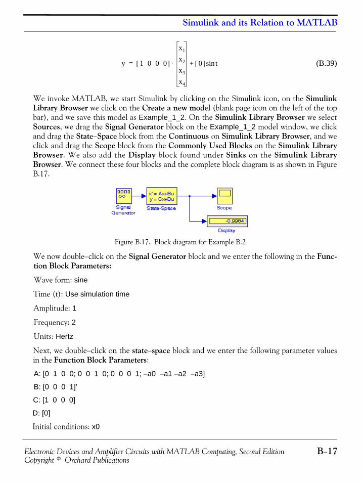
Electronic Devices and Amplifier Circuits with MATLAB Computing, Second Edition B−17Copyright © Orchard Publications
Simulink and its Relation to MATLAB
(B.39)
We invoke MATLAB, we start Simulink by clicking on the Simulink icon, on the SimulinkLibrary Browser we click on the Create a new model (blank page icon on the left of the topbar), and we save this model as Example_1_2. On the Simulink Library Browser we selectSources, we drag the Signal Generator block on the Example_1_2 model window, we clickand drag the State−Space block from the Continuous on Simulink Library Browser, and weclick and drag the Scope block from the Commonly Used Blocks on the Simulink LibraryBrowser. We also add the Display block found under Sinks on the Simulink LibraryBrowser. We connect these four blocks and the complete block diagram is as shown in FigureB.17.
Figure B.17. Block diagram for Example B.2
We now double−click on the Signal Generator block and we enter the following in the Func-tion Block Parameters:
Wave form: sine
Time (t): Use simulation time
Amplitude: 1
Frequency: 2
Units: Hertz
Next, we double−click on the state−space block and we enter the following parameter valuesin the Function Block Parameters:
A: [0 1 0 0; 0 0 1 0; 0 0 0 1; −a0 −a1 −a2 −a3]
B: [0 0 0 1]’
C: [1 0 0 0]
D: [0]
Initial conditions: x0
y 1 0 0 0[ ]
x1
x2
x3
x4
⋅ 0[ ] tsin+=
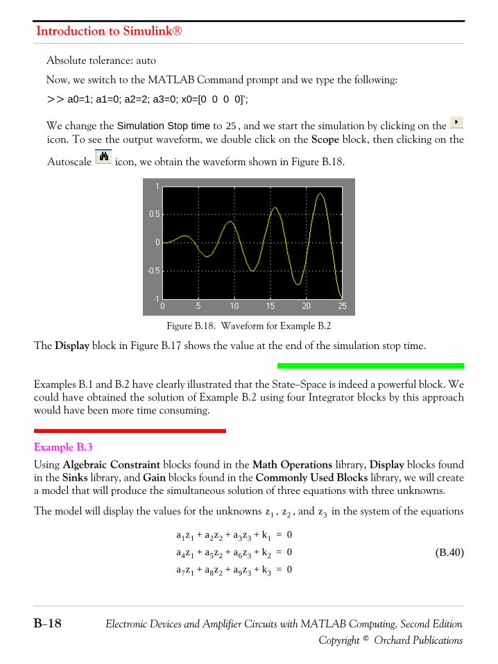
Introduction to Simulink®
B−18 Electronic Devices and Amplifier Circuits with MATLAB Computing, Second EditionCopyright © Orchard Publications
Absolute tolerance: auto
Now, we switch to the MATLAB Command prompt and we type the following:
>> a0=1; a1=0; a2=2; a3=0; x0=[0 0 0 0]’;
We change the Simulation Stop time to , and we start the simulation by clicking on the icon. To see the output waveform, we double click on the Scope block, then clicking on the
Autoscale icon, we obtain the waveform shown in Figure B.18.
Figure B.18. Waveform for Example B.2
The Display block in Figure B.17 shows the value at the end of the simulation stop time.
Examples B.1 and B.2 have clearly illustrated that the State−Space is indeed a powerful block. Wecould have obtained the solution of Example B.2 using four Integrator blocks by this approachwould have been more time consuming.
Example B.3 Using Algebraic Constraint blocks found in the Math Operations library, Display blocks foundin the Sinks library, and Gain blocks found in the Commonly Used Blocks library, we will createa model that will produce the simultaneous solution of three equations with three unknowns.
The model will display the values for the unknowns , , and in the system of the equations
(B.40)
25
z1 z2 z3
a1z1 a2z2 a3z3 k1+ + + 0=
a4z1 a5z2 a6z3 k2+ + + 0=
a7z1 a8z2 a9z3 k3+ + + 0=
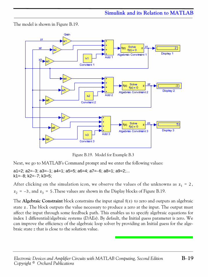
Electronic Devices and Amplifier Circuits with MATLAB Computing, Second Edition B−19Copyright © Orchard Publications
Simulink and its Relation to MATLAB
The model is shown in Figure B.19.
Figure B.19. Model for Example B.3
Next, we go to MATLAB’s Command prompt and we enter the following values:
a1=2; a2=−3; a3=−1; a4=1; a5=5; a6=4; a7=−6; a8=1; a9=2;...k1=−8; k2=−7; k3=5;
After clicking on the simulation icon, we observe the values of the unknowns as ,, and .These values are shown in the Display blocks of Figure B.19.
The Algebraic Constraint block constrains the input signal to zero and outputs an algebraicstate . The block outputs the value necessary to produce a zero at the input. The output mustaffect the input through some feedback path. This enables us to specify algebraic equations forindex 1 differential/algebraic systems (DAEs). By default, the Initial guess parameter is zero. Wecan improve the efficiency of the algebraic loop solver by providing an Initial guess for the alge-braic state z that is close to the solution value.
z1 2=
z2 3–= z3 5=
f z( )z

Introduction to Simulink®
B−20 Electronic Devices and Amplifier Circuits with MATLAB Computing, Second EditionCopyright © Orchard Publications
An outstanding feature in Simulink is the representation of a large model consisting of manyblocks and lines, to be shown as a single Subsystem block.* For instance, we can group all blocksand lines in the model of Figure B.19 except the display blocks, we choose Create Subsystemfrom the Edit menu, and this model will be shown as in Figure B.20† where in MATLAB’s Com-mand prompt we have entered:
a1=5; a2=−1; a3=4; a4=11; a5=6; a6=9; a7=−8; a8=4; a9=15;...k1=14; k2=−6; k3=9;
Figure B.20. The model of Figure B.19 represented as a subsystem
The Display blocks in Figure B.20 show the values of , , and for the values specified inMATLAB’s Command prompt.
B.2 Simulink DemosAt this time, the reader with no prior knowledge of Simulink, should be ready to learn Simulink’sadditional capabilities. It is highly recommended that the reader becomes familiar with the blocklibraries found in the Simulink Library Browser. Then, the reader can follow the steps delineatedin The MathWorks Simulink User’s Manual to run the Demo Models beginning with the thermomodel. This model can be seen by typing
thermo
in the MATLAB Command prompt.
* The Subsystem block is described in detail in Chapter 2, Section 2.1, Page 2−2, Introduction to Simulink withEngineering Applications, ISBN 978−1−934404−09−6.
† The contents of the Subsystem block are not lost. We can double−click on the Subsystem block to see its con-tents. The Subsystem block replaces the inputs and outputs of the model with Inport and Outport blocks. Theseblocks are described in Section 2.1, Chapter 2, Page 2−2, Introduction to Simulink with Engineering Applica-tions, 978−1−934404−09−6.
z1 z2 z3

Electronic Devices and Amplifier Circuits with MATLAB Computing, Second Edition C−1Copyright © Orchard Publications
Appendix C
Proportional−Integral−Derivative (PID) Controller
his appendix is a brief introduction to the Proportional−Integral−Derivative Controller,briefly known as PID. The components and the functions of a typical PID are described,and two examples are presented using the Simulink PID Controller Block and the Simulink
PID Controller with Approximate Derivative Block.
C.1 Description and Components of a Typical PIDA proportional−integral−derivative (PID) controller is a control loop feedback system used inindustrial control systems. A PID controller attempts to correct the error between a measuredprocess variable and a desired setpoint by calculating and then outputting a corrective action thatcan adjust the process accordingly.
The PID controller calculation contains three separate parameters; the Proportional, the Inte-gral, and Derivative values as shown in Figure C.1.
Figure C.1. The components of a typical PID
The Proportional value determines the reaction to the current error, the Integral determines thereaction based on the sum of recent errors, and the Derivative determines the reaction to the rateat which the error has been changing. The weighted sum of these three actions is used to adjustthe process via a control element such as the position of a control valve or the power supply of aheating element.
By adjusting the three constants in the PID controller algorithm the PID can provide controlaction designed for specific process requirements. The response of the controller can be described
T
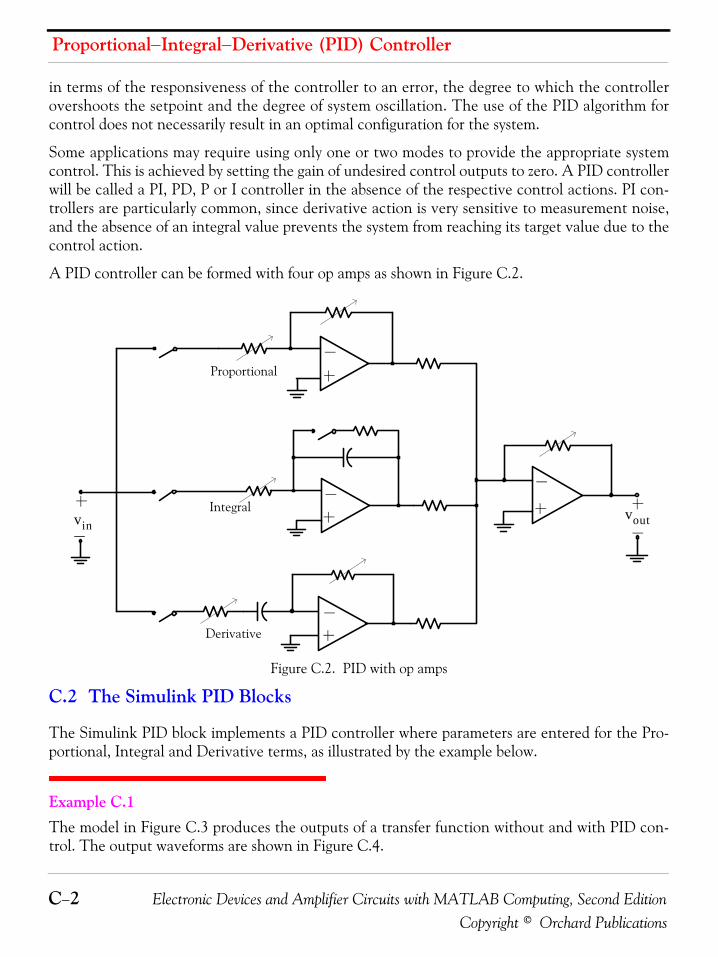
Proportional−Integral−Derivative (PID) Controller
C−2 Electronic Devices and Amplifier Circuits with MATLAB Computing, Second EditionCopyright © Orchard Publications
in terms of the responsiveness of the controller to an error, the degree to which the controllerovershoots the setpoint and the degree of system oscillation. The use of the PID algorithm forcontrol does not necessarily result in an optimal configuration for the system.
Some applications may require using only one or two modes to provide the appropriate systemcontrol. This is achieved by setting the gain of undesired control outputs to zero. A PID controllerwill be called a PI, PD, P or I controller in the absence of the respective control actions. PI con-trollers are particularly common, since derivative action is very sensitive to measurement noise,and the absence of an integral value prevents the system from reaching its target value due to thecontrol action.
A PID controller can be formed with four op amps as shown in Figure C.2.
Figure C.2. PID with op amps
C.2 The Simulink PID Blocks
The Simulink PID block implements a PID controller where parameters are entered for the Pro-portional, Integral and Derivative terms, as illustrated by the example below.
Example C.1 The model in Figure C.3 produces the outputs of a transfer function without and with PID con-trol. The output waveforms are shown in Figure C.4.
vinvout
Proportional
Integral
Derivative
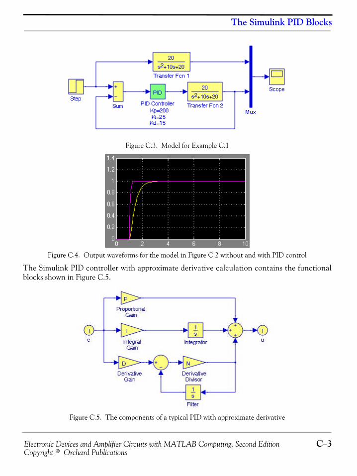
Electronic Devices and Amplifier Circuits with MATLAB Computing, Second Edition C−3Copyright © Orchard Publications
The Simulink PID Blocks
Figure C.3. Model for Example C.1
Figure C.4. Output waveforms for the model in Figure C.2 without and with PID control
The Simulink PID controller with approximate derivative calculation contains the functionalblocks shown in Figure C.5.
Figure C.5. The components of a typical PID with approximate derivative

Proportional−Integral−Derivative (PID) Controller
C−4 Electronic Devices and Amplifier Circuits with MATLAB Computing, Second EditionCopyright © Orchard Publications
Example C.2 The model in Figure C.6 produces the outputs of a transfer function without and with PID controlwith approximate derivative. The output waveforms are shown in Figure C.7.
Figure C.6. Model for Example C.2
Figure C.7. Output waveforms for the model in Figure C.6 without and with PID control
The reader should try to minimize the oscillations shown in Figure C.7 by assigning other valuesfor the Derivative divisor.
The examples presented in this appendix indicate that the Proportional Gain , Integral Gain, and Derivative Gain are dependent on each another. Generally, and will decrease
the rise time and increase the overshoot, and will cause a small change in rise time anddecrease the overshoot.
KpKi Kd Kp Ki
Kd
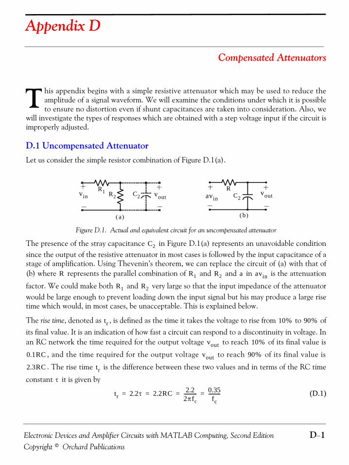
Electronic Devices and Amplifier Circuits with MATLAB Computing, Second Edition D−1Copyright © Orchard Publications
Appendix D
Compensated Attenuators
his appendix begins with a simple resistive attenuator which may be used to reduce theamplitude of a signal waveform. We will examine the conditions under which it is possibleto ensure no distortion even if shunt capacitances are taken into consideration. Also, we
will investigate the types of responses which are obtained with a step voltage input if the circuit isimproperly adjusted.
D.1 Uncompensated AttenuatorLet us consider the simple resistor combination of Figure D.1(a).
Figure D.1. Actual and equivalent circuit for an uncompensated attenuator
The presence of the stray capacitance in Figure D.1(a) represents an unavoidable conditionsince the output of the resistive attenuator in most cases is followed by the input capacitance of astage of amplification. Using Thevenin’s theorem, we can replace the circuit of (a) with that of(b) where represents the parallel combination of and and in is the attenuation
factor. We could make both and very large so that the input impedance of the attenuatorwould be large enough to prevent loading down the input signal but his may produce a large risetime which would, in most cases, be unacceptable. This is explained below.
The rise time, denoted as , is defined as the time it takes the voltage to rise from to ofits final value. It is an indication of how fast a circuit can respond to a discontinuity in voltage. Inan RC network the time required for the output voltage to reach of its final value is
, and the time required for the output voltage to reach of its final value is
. The rise time is the difference between these two values and in terms of the RC time
constant it is given by
(D.1)
T
R2R
vin C2
R1avin
voutvoutC2
a( ) b( )
C2
R R1 R2 a avin
R1 R2
tr 10% 90%
vout 10%
0.1RC vout 90%
2.3RC trτ
tr 2.2τ 2.2RC 2.22πfc----------- 0.35
fc----------= = = =
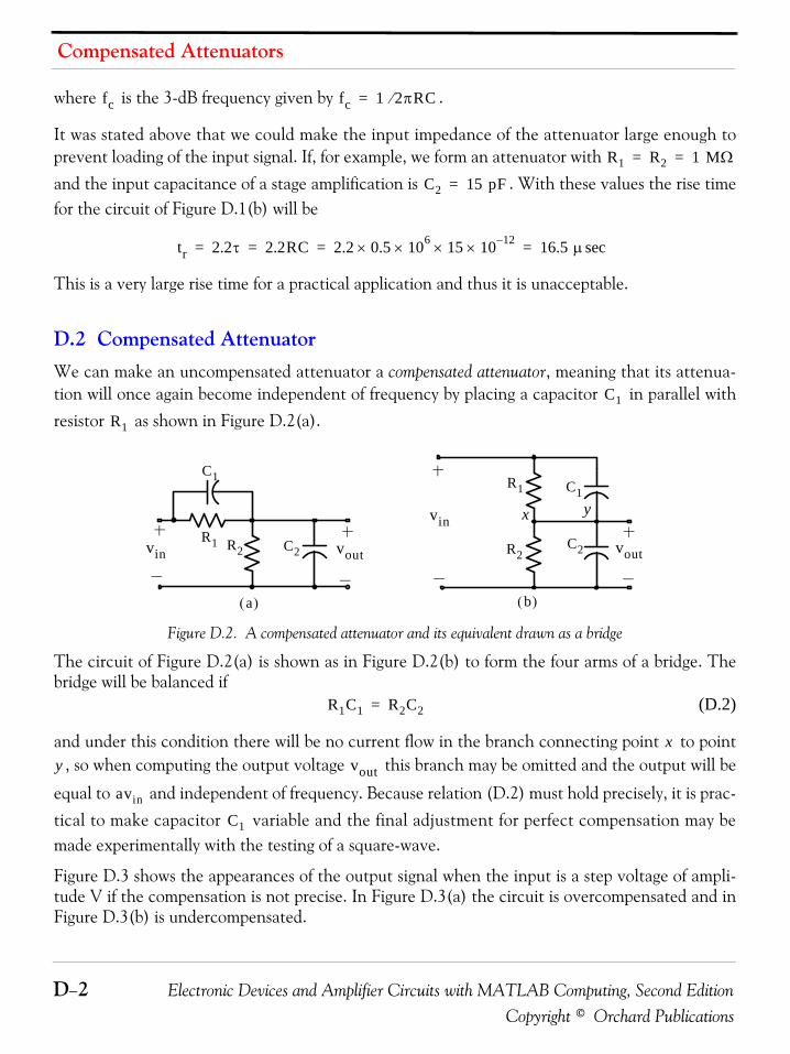
Compensated Attenuators
D−2 Electronic Devices and Amplifier Circuits with MATLAB Computing, Second EditionCopyright © Orchard Publications
where is the 3-dB frequency given by .
It was stated above that we could make the input impedance of the attenuator large enough toprevent loading of the input signal. If, for example, we form an attenuator with and the input capacitance of a stage amplification is . With these values the rise timefor the circuit of Figure D.1(b) will be
This is a very large rise time for a practical application and thus it is unacceptable.
D.2 Compensated AttenuatorWe can make an uncompensated attenuator a compensated attenuator, meaning that its attenua-tion will once again become independent of frequency by placing a capacitor in parallel withresistor as shown in Figure D.2(a).
Figure D.2. A compensated attenuator and its equivalent drawn as a bridge
The circuit of Figure D.2(a) is shown as in Figure D.2(b) to form the four arms of a bridge. Thebridge will be balanced if
(D.2)
and under this condition there will be no current flow in the branch connecting point to point, so when computing the output voltage this branch may be omitted and the output will be
equal to and independent of frequency. Because relation (D.2) must hold precisely, it is prac-tical to make capacitor variable and the final adjustment for perfect compensation may bemade experimentally with the testing of a square-wave.
Figure D.3 shows the appearances of the output signal when the input is a step voltage of ampli-tude V if the compensation is not precise. In Figure D.3(a) the circuit is overcompensated and inFigure D.3(b) is undercompensated.
fc fc 1 2πRC⁄=
R1 R2 1 MΩ= =
C2 15 pF=
tr 2.2τ 2.2RC 2.2 0.5 106 15 10 12–×××× 16.5 μ sec= = = =
C1
R1
R1 R2 C2
C1
vin
vin vout voutC2
C1R1
R2
a( ) b( )
yx
R1C1 R2C2=
xy vout
avin
C1
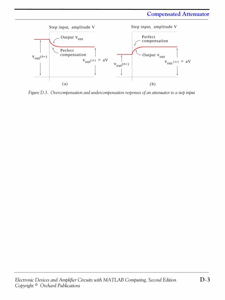
Electronic Devices and Amplifier Circuits with MATLAB Computing, Second Edition D−3Copyright © Orchard Publications
Compensated Attenuator
Figure D.3. Overcompensation and undercompensation responses of an attenuator to a step input
Step input amplitude V, Step input amplitude V,
Perfectcompensation
Perfectcompensation
Output vout
Output voutvout 0+( )
vout 0+( )vout ∞( ) aV= vout ∞( ) aV=
a( ) b( )

Compensated Attenuators
D−4 Electronic Devices and Amplifier Circuits with MATLAB Computing, Second EditionCopyright © Orchard Publications
NOTES:

Electronic Devices and Amplifier Circuits with MATLAB Computing, Second Edition E−1Copyright © Orchard Publications
Appendix E
Substitution, Reduction, and Miller’s Theorems
his appendix discusses three additional theorems that are especially useful in the simplifica-tion of circuits containing dependent sources. In our previous studies* we discussed thesuperposition principle and Thevenin’s and Norton’s theorems.
E.1 The Substitution Theorem
The substitution theorem states that if the voltage across a branch with nodes and of a networkis and the current through this branch is , a different branch may be substituted in its
place in the network provided that the voltage across the substitute branch is also and the
current through it is also . The most common use of this theorem is to replace an impedanceby a voltage or current source, or vice versa. The substitution theorem can best illustrated withthe simple circuit and the substitute branches shown in Figure E.1.
Figure E.1. Illustration of the substitution theorem
For the simple resistor circuit of Figure E.1(a) we find by series−parallel resistance combinationsthat and . According to the substitution theorem, the resistor across
terminals and can be replaced with a source with a source as shown in Figure E.1(b) andthe rest of the network will be unaffected. The current in the branch will be as before.
Other substitutions are possible also. For instance, the substitute branch may consist of a resis-tance of and a voltage source of as shown in Figure E.1(c), or it may consist of a resis-tance of and a voltage source of of opposite polarity as shown in Figure E.1(d).
* For a detailed discussion of Thevenin’s and Norton’s theorems and the superposition principle please refer toCircuit Analysis I with MATLAB Applications, ISBN 978−0−9709511−2−0.
Tx y
vxy ixy
vxy
ixy
a( )
24 V y
xx x x x
y yyy
4 Ω
b( ) e( )d( )c( )
2 Ω
2 Ω
2 Ω
vxy 6 V=ixy 3 A=
3 A
6 V
1 Ω
3 V 3 V
3 Ω XC 8 3⁄ Ω=
V' 10 53.1° ∠ V=
vxy 6 V= ixy 3 A= 2 Ω
x y 6 V3 A
1 Ω 3 V3 Ω 3 V
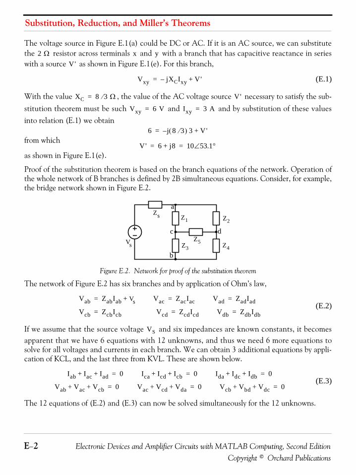
Substitution, Reduction, and Miller’s Theorems
E−2 Electronic Devices and Amplifier Circuits with MATLAB Computing, Second EditionCopyright © Orchard Publications
The voltage source in Figure E.1(a) could be DC or AC. If it is an AC source, we can substitutethe resistor across terminals and with a branch that has capacitive reactance in serieswith a source as shown in Figure E.1(e). For this branch,
(E.1)
With the value , the value of the AC voltage source necessary to satisfy the sub-stitution theorem must be such and and by substitution of these valuesinto relation (E.1) we obtain
from which
as shown in Figure E.1(e).
Proof of the substitution theorem is based on the branch equations of the network. Operation ofthe whole network of B branches is defined by 2B simultaneous equations. Consider, for example,the bridge network shown in Figure E.2.
Figure E.2. Network for proof of the substitution theorem
The network of Figure E.2 has six branches and by application of Ohm’s law,
(E.2)
If we assume that the source voltage and six impedances are known constants, it becomesapparent that we have 6 equations with 12 unknowns, and thus we need 6 more equations tosolve for all voltages and currents in each branch. We can obtain 3 additional equations by appli-cation of KCL, and the last three from KVL. These are shown below.
(E.3)
The 12 equations of (E.2) and (E.3) can now be solved simultaneously for the 12 unknowns.
2 Ω x yV'
Vxy jXCIxy– V'+=
XC 8 3 Ω⁄= V'
Vxy 6 V= Ixy 3 A=
6 j 8 3⁄( )– 3 V'+=
V' 6 j8+ 10 53.1°∠= =
a
Vs
Zs Z1 Z2
Z3 Z4Z5
b
c d
Vab ZabIab Vs+= Vac ZacIac= Vad ZadIad=
Vcb ZcbIcb= Vcd ZcdIcd= Vdb ZdbIdb=
VS
Iab Iac Iad+ + 0= Ica Icd Icb+ + 0= Ida Idc Idb+ + 0=
Vab Vac Vcb+ + 0= Vac Vcd Vda+ + 0= Vcb Vbd Vdc+ + 0=

Electronic Devices and Amplifier Circuits with MATLAB Computing, Second Edition E−3Copyright © Orchard Publications
The Substitution Theorem
From the foregoing discussion we conclude that it is possible to write as many equations as thereare unknowns. Thus, if the number of branches is B, the number of unknowns is 2B. Let us nowsuppose that the branch for which substitution is to be made contains an impedance and a sourceand the equation for this branch is
(E.4)
that is, the voltage across this branch is and the current is . Other branch voltages in the
network are , , and so on, and currents are , , and so on, and all these voltages andcurrents simultaneously satisfy the 2B equations of the network, including equation (E.4).
Next, let us assume a substitute branch that has some different value of impedance , and
some different voltage source , but with and so related that the same values of
and that satisfied equation (E.4) will also satisfy the new branch equation
(E.5)
When this substitution is made, operation of the altered network will be defined by 2B equations,as before; (2B − 1) of the equations will remain the same but equation (E.5) will have replacedequation (E.4). However, since equation (E.5) is satisfied by the same values of voltage and cur-rent that satisfied equation (E.4), it follows that the whole group of simultaneous equations will besatisfied by the same voltages and currents as before. Voltages and currents of all branches of thenetwork will therefore be the same as before substitution, which was to be proved.
The substitution theorem is especially useful in the simplification of circuits containing dependentsources. Consider for example the current−controlled voltage source and the voltage−controlledcurrent source shown in Figure E.3.
Figure E.3. Application of the substitution theorem in current− and voltage−controlled dependent sources.
The network of Figure E.3(a) can be any network having the terminal current , and is thevoltage of a current−controlled voltage source. Figure E.3(b) shows the conditions under whichthe dual form can be applied. In this case the voltage−controlled current source , which is con-nected across the voltage . As another example, let us consider the equivalent circuit of someamplifier shown in Figure E.4(a).
Vab ZabIab VS+=
Vab Iab
Vbc Vcd Ibc Icd
Z'ab
V'S Z'ab V'S Vab
Iab
Vab Z'abIab V'S+=
Rest of thenetwork
Rest of thenetwork
Ri
i
Gvv
a( ) b( )
i Ri
Gvv

Substitution, Reduction, and Miller’s Theorems
E−4 Electronic Devices and Amplifier Circuits with MATLAB Computing, Second EditionCopyright © Orchard Publications
Figure E.4. Application of the substitution theorem in an amplifier equivalent circuit.
In Figure E.4(a), the currents and voltages are not changed if the dependent source isreplaced by a resistance , and the simplified equivalent circuit is as shown in Figure E.4(b).
A special case of the substitution theorem is the source absorption theorem* and has two dual forms,the voltage source absorption and the current source absorption theorems.
The voltage source absorption theorem is illustrated in Figure E.5.
Figure E.5. Illustration of the voltage source absorption theorem
As shown in Figure E.5, the voltage source absorption states that if in a branch of the network inwhich the current through it is , the voltage source can be replaced by an impedance .
Example E.1
Use the voltage source absorption theorem to simplify the branch shown in Figure E.6.
Figure E.6. Branch for Example E.1 to be simplified
* This theorem is analogous to the absorption theorem in Boolean algebra which states that
vinR1vin vout R1R2 1 μ+( )R2
R3 R3
R4 R4i
a( ) b( )
μR2i μvin μvin
vout
μR2i
μR2
A A B+( ) AB= =
a( ) b( )
ZiZ
ii
i Zi Z
AB
iA B
aZiZ

Electronic Devices and Amplifier Circuits with MATLAB Computing, Second Edition E−5Copyright © Orchard Publications
The Substitution Theorem
Solution:
Application of the voltage source absorption theorem yields the simplified branch shown in FigureE.7(c) below.
Figure E.7. Steps for simplification of the branch for Example E.1
The current source absorption theorem is illustrated in Figure E.8.
Figure E.8. Illustration of the current source absorption theorem
As shown in Figure E.8, the current source absorption states that if in a branch of the network inwhich the voltage across it is , the current source can be replaced by an admittance .
Example E.2 Use the current source absorption theorem to simplify the parallel combination shown in FigureE.9.
Figure E.9. Branch for Example E.2 to be simplified
Solution:
Application of the current source absorption theorem yields the simplified branch shown in FigureE.10(c) below.
iA B
aZiZ
A AB Bi i
Z aZ
a 1+( )Z
a( ) b( ) c( )
a( ) b( )
Yv
YA B BA
v vAB=v vAB=
v Yv Y
A B
aYvAB
Y

Substitution, Reduction, and Miller’s Theorems
E−6 Electronic Devices and Amplifier Circuits with MATLAB Computing, Second EditionCopyright © Orchard Publications
Figure E.10. Steps for simplification of the parallel combination of Example E.2
E.2 The Reduction TheoremThe reduction theorem is essentially an extension of the substitution theorem. This theorem appliesto network configurations such as those shown in Figure E.11.
Figure E.11. Network configurations that can be simplified by the reduction theorem
The reduction theorem applies to the network configurations shown in Figure E.11. The network in Figure E.11(a) is any linear two−terminal network having the terminal voltage , and
is any other linear two−terminal network. The constant of the voltage−controlled voltagesource is any real number, positive or negative. The two networks and the voltage source areconnected in series so that the voltages and are additive with respect to the loop that theyform. The theorem states that all currents in and remain unchanged if the source isreplaced with a short circuit and if:
1. Each resistance, inductance, reciprocal capacitance, and voltage source in Network is mul-tiplied by
or
2. Each resistance, inductance, reciprocal capacitance, and voltage source in Network isdivided by .
Proof of the reduction theorem is based on the form of the loop equations. Obviously, if all resis-tances, inductances, reciprocal capacitances, and voltage sources are multiplied by the same arbi-
A B
aYvAB
Y
A
A
B
B
a 1+( )Y
a( ) b( ) c( )
Y
aY
Rest of the Rest of the Rest of the Rest of thenetwork N1 network N2
network N1 network N2
a( ) b( )
Ai1
i1 1 A+( )i1
v1 1 A+( )v1
Av1
N1 v1 N2
AAv1
v1 Av1
N1 N2 Av1
N1
1 A+
N2
1 A+

Electronic Devices and Amplifier Circuits with MATLAB Computing, Second Edition E−7Copyright © Orchard Publications
The Reduction Theorem
trary factor, then every term in the set of loop equations is multiplied by the same factor, and allthe loop currents remain unchanged. Thus, if all the parameters and voltage sources in aremultiplied by as specified in Part 1 of the theorem, and if is replaced with a short cir-cuit, then the voltage applied to is still , and all currents in and remainunchanged. All voltages in are multiplied by the factor , but the voltages in are notchanged. Any current sources in and are left unchanged in the reduction process.
By the same reasoning process, after the transformation described above is completed, all resis-tances, inductances, reciprocal capacitances, and voltage sources in the composite network −
can be divided by the factor without changing any of the currents in − . Thus,Part 2 of the theorem is proved.
When all currents and voltages in the network are sinusoidal and of the same frequency, the con-stant of the controlled source may be expressed as a complex number; the reduction theoremholds in this case also.
The dual form of the reduction theorem is applicable to the network configuration shown in Fig-ure E.11(b). It states that all voltages in the network of Figure E.11(b) remain unchanged if thecurrent source is replaced with an open circuit and if:
1. All conductances, capacitances, reciprocal inductances, and current sources in are multi-plied by
or
2. All conductances, capacitances, reciprocal inductances, and current sources in are dividedby
Proof of the dual form of the theorem follows from nodal equations and is dual to the proof out-lined above. In applying the reduction theorem it is essential that the two networks and beproperly identified before application of this theorem. The two necessary requirements are:
a. The terminal voltage (or current) of the network identified as Network must be the con-trolling quantity for the source to be eliminated; and
b. No current may enter or leave either network through any terminal other than the two termi-nals by which the networks and controlled source are joined in series (or parallel). It should benoted that connections joining separate parts of a network carry no current and can thereforebe ignored in respect to item b.
A useful application of the reduction theorem is provided by the cascode amplifier shown in FigureE.12.
N1
1 A+ Av1
N2 1 A+( )v1 N1 N2
N1 1 A+ N2
N1 N2
N1
N2 1 A+ N1 N2
Ai1
N1
1 A+
N2
1 A+
N1 N2
N1

Substitution, Reduction, and Miller’s Theorems
E−8 Electronic Devices and Amplifier Circuits with MATLAB Computing, Second EditionCopyright © Orchard Publications
Figure E.12. Typical cascode amplifier with BJTs
Figure E.12 shows a partial circuit of a cascode amplifier where a common−base bipolar transistorsits on top of a common−emitter bipolar transistor. Of course, a cascode amplifier may use MOS-FETs of CMOS devices. To illustrate an application of the reduction theorem, let us consider thethe incremental model of some cascode amplifier shown in Figure E.13.
Figure E.13. Incremental model of a cascode amplifier and simplification by application of the reduction theorem
vin
vin
vin
vg1
R1
R1
R1
a( )
b( )
c( )
1 μ+( )2R2
1 μ+( )R2
R2
μvin
μ 1 μ+( )vin
i
μvg1 R3
vg2
v3μvg2
vout
vout
vout
R4
R3
R3μv3
1 μ+( )v3
R3
Network 1 Network 2
1 μ+( )R3
R3
R41 μ+( )v3
v3
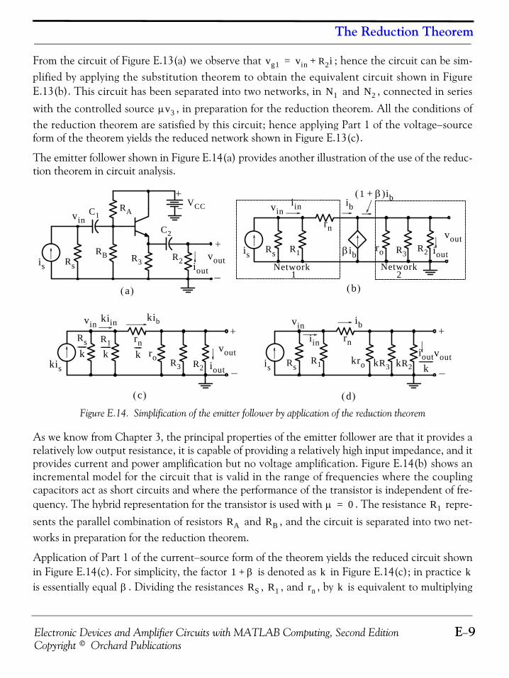
Electronic Devices and Amplifier Circuits with MATLAB Computing, Second Edition E−9Copyright © Orchard Publications
The Reduction Theorem
From the circuit of Figure E.13(a) we observe that ; hence the circuit can be sim-plified by applying the substitution theorem to obtain the equivalent circuit shown in FigureE.13(b). This circuit has been separated into two networks, in and , connected in serieswith the controlled source , in preparation for the reduction theorem. All the conditions ofthe reduction theorem are satisfied by this circuit; hence applying Part 1 of the voltage−sourceform of the theorem yields the reduced network shown in Figure E.13(c).
The emitter follower shown in Figure E.14(a) provides another illustration of the use of the reduc-tion theorem in circuit analysis.
Figure E.14. Simplification of the emitter follower by application of the reduction theorem
As we know from Chapter 3, the principal properties of the emitter follower are that it provides arelatively low output resistance, it is capable of providing a relatively high input impedance, and itprovides current and power amplification but no voltage amplification. Figure E.14(b) shows anincremental model for the circuit that is valid in the range of frequencies where the couplingcapacitors act as short circuits and where the performance of the transistor is independent of fre-quency. The hybrid representation for the transistor is used with . The resistance repre-sents the parallel combination of resistors and , and the circuit is separated into two net-works in preparation for the reduction theorem.
Application of Part 1 of the current−source form of the theorem yields the reduced circuit shownin Figure E.14(c). For simplicity, the factor is denoted as in Figure E.14(c); in practice is essentially equal . Dividing the resistances , , and , by is equivalent to multiplying
vg1 vin R2i+=
N1 N2
μv3
vin
d( )
voutR2
kR3
R3
Network2
c( )
b( )a( )
1Network
R2R3
C1
Rsis
vin
vin vin
is Rs R1
rn
rn
kroro
ro
vout
vout vout
iout
ioutk
--------iout
iout
kis is
R1k
------Rs
R1 kR2
R2R3
RA
RB
VCC
C2
iin
kiin
iin1 β+( )ibib
βib
ibkib
Rsk-----
rnk----
μ 0= R1
RA RB
1 β+ k kβ RS R1 rn k

Substitution, Reduction, and Miller’s Theorems
E−10 Electronic Devices and Amplifier Circuits with MATLAB Computing, Second EditionCopyright © Orchard Publications
the corresponding conductances by this factor. Thus, application of the reduction theorem yieldsthe simplified circuit of Figure E.14(c).
The current amplification of the circuit is accounted for by the fact that the input signal current ismultiplied by the factor in the reduced circuit. It is clear from Figure E.14(c) that the forwardvoltage transmittance of the emitter follower is less than unity, and for large values of the out-put resistance of the emitter follower is very small.
If Part 2 of the theorem is applied instead of Part 1, the circuit of Figure E.14(d) is obtained; thiscircuit is convenient for studying relations at the input terminals since the input voltage and cur-rent are unmodified. For large values of the output resistance of the emitter follower is verylarge.
E.3 Miller’s Theorem
Miller’s theorem states that under certain conditions, to be established below, the networks of Fig-ures E.15(a) and E.15(b) are equivalent.
Figure E.15. Illustration for Miller’s theorem
In the networks of Figure E.15, the constant denotes the voltage gain from Node A to Node B,that is,
(E.6)
or(E.7)
At Node of Figure E.15(a), we observe that
(E.8)
and at Node of Figure E.15(b), we obtain,
(E.9)
For equivalence, relations (E.8) and (E.9) must be equal. Thus,
(E.10)
kβ
β
AA B
B
v2 Kv1=Y1
YY2
v1v1v2 Kv1=
a( ) b( )
i1i2i1i2
K
K v2 v1⁄=
v2 Kv1=
A
i1 Y vA vB–( ) Y v1 v2–( ) Y v1 Kv1–( ) Yv1 1 K–( )= = = =
A
i1 Y1v1=
Y1 Y 1 K–( )=

Electronic Devices and Amplifier Circuits with MATLAB Computing, Second Edition E−11Copyright © Orchard Publications
Miller’s Theorem
At Node of Figure E.15(a), we observe that
(E.11)
and at Node of Figure E.15(b), we obtain,
(E.12)
For equivalence, relations (E.11) and (E.12) must be equal. Thus,
(E.13)
We should remember that for the equivalent circuit of Figure E.15(b) the value of the gain ,once established, it cannot be changed. Thus, while Miller’s theorem can be applied to find theinput impedance, it should not be used to determine the output impedance of an amplifier sincewhen determining the output impedance the input signal voltage is normally set to zero volts.
Miller’s dual theorem states that under certain conditions, to be established below, the networks ofFigures E.16(a) and E.16(b) are equivalent.
Figure E.16. Illustration for Miller’s dual theorem
In the networks of Figure E.16, the constant denotes the current gain from Node A to Node B,that is,
(E.14)
or(E.15)
At Node of Figure E.16(a), we observe that
(E.16)
and at Node of Figure E.16(b), we obtain,
(E.17)
For equivalence, relations (E.16) and (E.17) must be equal. Thus,
B
i2 i1– Y– v1 v2–( ) Y v2 v1–( ) Y v2 v2 K⁄–( ) Yv2 1 1 K⁄–( )= = = = =
B
i2 Y2v2=
Y2 Y 1 1 K⁄–( )=
K
vS
AA B
B
v2Z1Z Z2
v1v1
a( ) b( )
i1i1i2 αi1=
v2
i2 αi1=
α
α i2 i1⁄=
i2 αi1=
A
v1 Z i1 i2+( ) Z i1 αi1+( ) Zi1 1 α+( )= = =
A
v1 Z1i1=

Substitution, Reduction, and Miller’s Theorems
E−12 Electronic Devices and Amplifier Circuits with MATLAB Computing, Second EditionCopyright © Orchard Publications
(E.18)
At Node of Figure E.16(a), we observe that
(E.19)
and at Node of Figure E.16(b), we obtain,
(E.20)
For equivalence, relations (E.19) and (E.20) must be equal. Thus,
(E.21)
Example E.3
For the circuit of Figure E.17, it is given that . Use Miller’s theorem to replace thiscircuit with an equivalent circuit where resistor is being replaced with another resistor in par-allel with resistor . Make any reasonable assumptions.
Figure E.17. Circuit for Example E.3
Solution:
Since it is reasonable to assume that practically all the current of the current source flowsthrough resistor and thus the output voltage is
from which
Figure E.18 shows the equivalent circuit after application of Miller’s theorem where using relation(E.10) we obtain
Z1 Z 1 α+( )=
B
v2 v1 Zi1 1 α+( )= =
B
v2 Z2i2 Z2αi1= =
Z2 Z 1 1 α⁄+( )=
R1 100R2=
R1
RS
isRs
R1R2
voutgmv1
v1
R1 R2»
R2
vout gmv1R2– Kv1= =
K gmR2–=
R'1 R1 1 K–( )⁄ R1 1 gmR2+( )⁄= =
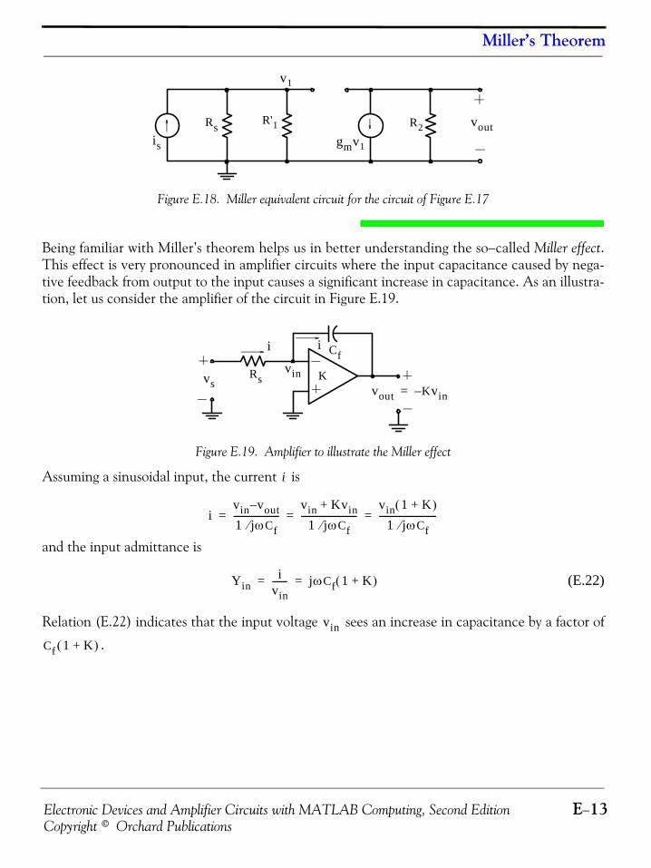
Electronic Devices and Amplifier Circuits with MATLAB Computing, Second Edition E−13Copyright © Orchard Publications
Miller’s Theorem
Figure E.18. Miller equivalent circuit for the circuit of Figure E.17
Being familiar with Miller’s theorem helps us in better understanding the so−called Miller effect.This effect is very pronounced in amplifier circuits where the input capacitance caused by nega-tive feedback from output to the input causes a significant increase in capacitance. As an illustra-tion, let us consider the amplifier of the circuit in Figure E.19.
Figure E.19. Amplifier to illustrate the Miller effect
Assuming a sinusoidal input, the current is
and the input admittance is
(E.22)
Relation (E.22) indicates that the input voltage sees an increase in capacitance by a factor of
.
is
Rs R'1
v1
gmv1
R2 vout
i
vsRs
vout Kvin–=Kvin
i Cf
i
ivin vout–
1 jωCf⁄---------------------
vin Kvin+
1 jωCf⁄-------------------------
vin 1 K+( )
1 jωCf⁄--------------------------= = =
Yini
vin------- jωCf 1 K+( )= =
vin
Cf 1 K+( )
Substitution, Reduction, and Miller’s Theorems
E−14 Electronic Devices and Amplifier Circuits with MATLAB Computing, Second EditionCopyright © Orchard Publications
NOTES:
Electronic Devices and Amplifier Circuits MATLAB ® Computing , Second Edition R−1Copyright © Orchard Publications
References and Suggestions for Further StudyA. Manufacturers Data Books and Sheets
1. Fairchild TTL Data Book, Fairchild Semiconductor, http://www.fairchildsemi.com/
2. Texas Instruments TTL Data Book, Texas Instruments, http://www.ti.com/
3. MECL Device Data, Motorola, http://www.motorola.com/home/
4. Transistor Manual, General Electric, http://www.ge.com/en/
5. Rectifiers and Zener Diodes Data Book, Motorola, ISBN 9−9991969−7−7
6. SCR Manual, General Electric, ISBN 0−1379676−3−2
7. LM 555 Timer, National Semiconductor, http://www.national.com/ds/LM/LM555.pdf
B. Texts and Handbooks
1. Reference Data for Engineers Radio, Electronics, Computer & Communications, ISBN 0−7506729−1−9
2. Electronic Circuits, E.J. Angelo, Jr. Mc-Graw-Hill Book Co.
3. Microelectronic Circuits, Oxford University Press, ISBN 0−19-511663−1
4. Standard Handbook of Electronic Engineering, ISBN 0−0713842−1−95. Mathematics for Business, Science, and Technology, ISBN 978−1−934404−01−0
6. Numerical Analysis Using MATLAB® and Excel, ISBN 978−1−934404−03−4
7. Circuit Analysis I with MATLAB® Applications, ISBN 978−0−9709511−2−0
8. Circuit Analysis II with MATLAB® Applications, ISBN 978−0−9709511−5−1
9. Signals and systems with MATLAB® Computing and Simulink® Modeling, ISBN 978−1−934404−11−9
10. Digital Circuit Analysis and Design with Simulink Applications and Introduction to CPLDs andFPGAs, ISBN 978−1−934404−05−8
11. Introduction to Simulink® with Engineering Applications, ISBN 978−1−934404−09−6
12. Introduction to Stateflow® with Applications, ISBN 978−1−934404−07−2

R−2 Electronic Devices and Amplifier Circuits MATLAB ® Computing , Second EditionCopyright © Orchard Publications
C. The following publications by The MathWorks, are highly recommended for further study. They are available from The MathWorks, 3 Apple Hill Drive, Natick, MA, 01760, www.mathworks.com.
1. Getting Started with MATLAB®
2. Using MATLAB®
3. Using MATLAB® Graphics
4. Using Simulink®
5. Sim Power Systems for Use with Simulink®
6. Fixed−Point Toolbox
7. Simulink® Fixed−Point
8. Real−Time Workshop
9. Signal Processing Toolbox
10. Getting Started with Signal Processing Blockset
11. Signal Processing Blockset
12. Control System Toolbox
13. Stateflow®

Index% (percent) symbol in MATLAB A-2 C source absorption E-4555 Timer 7-2 cutoff
cascaded tuned amplifiers 9-14 frequency 1-5, 5-8A cascode amplifier E-7 region inA/D conversion 5-56 cathode 2-6 bipolar transistors 3-78abs(z) MATLAB function A-23 cesium oscillators 10-8 MOSFETs 4-9accuracy defined 5-62 Class UJTs 4-23active A Amplifier 3-31 filter 5-8 AB Amplifier 3-35 D mode 3-3 B Amplifier 3-34 pull-up 6-18 C Amplifier 3-37 D/A converter 5-53 region 3-78 D amplifier 3-38 DAC withADC 5-56 E amplifier 3-38 with binary-weighted resistors 5-53Advanced Low-Power clc MATAB command A-2 buffered output and gain 5-56 Schottky devices 6-41 clear MATLAB command A-2 Darlington connection 3-60alternating waveform 1-2 closed loop dataamount of feedback 10-2 gain 5-27 bus 6-38amplifier defined 1-3 transfer function 5-30 points in MATLAB A-14amplitude-modulated signal 9-2 CMOS sheets from manufacturers 6-20analog computers 5-63 defined 4-19 dB defined 1-4analog-to-digital converter 5-56 Inverter 6-33 decade defined 1-7AND gate 6-1 Logic Gates 6-32 decibel defined 1-4angle(z) MATLAB function A-25 NAND Gate 6-34 deconv(c,d) MATLAB function A-6anode 2-6 NOR Gate 6-35 default settings in MATLAB A-13, A-16Armstrong oscillator 10-6 transmission gate 6-37 degenerative feedback 5-25, 10-2astable multivibrator 7-1 CMRR 5-41 depletionattenuation factor 7-13 Colpitts oscillator 10-7 region 2-4attenuator 1-4 column vector in MATLAB A-19 mode 4-7avalanche 2-8 command window in MATLAB A-1 diac 4-23average value defined 1-1 commas in MATLAB A-8 differentialaveraging op amp 5-37 comment line in MATLAB A-2 circuit 6-24axis MATLAB command A-16 common gain 5-41
base current gain 3-5 inputB collector current gain 3-5 amplifier 5-1
emitter gain 3-4 integrator 5-76backward diode 2-47 common mode op amp 5-39band-elimination filter 5-10 gain 5-41 differentiator 5-35bandpass rejection ratio 5-41 digital-to-analog converter 5-53 amplifier 9-4 comparator 5-25, 5-50 diode filter 5-10, 9-1 compensated attenuator D-2 detector 2-37, 9-2band-rejection filter 5-10 Complementary Metal Oxide ideal characteristics of 2-6band-stop filter 5-10 Semiconductor 4-19, 6-2 display formats in MATLAB A-32bandwidth defined 1-5 complementary MOS 4-19 doping 3Barkhausen criterion 10-4 complex dot multiplication operatorbarrier 2-5 conjugate A-4 in MATLAB A-22base spreading resistance 3-45 numbers in MATLAB A-3 drain 4-1basic differentiator circuit 5-35 conduction angle in SCR 4-26 driver gate 6-18beta cutoff frequency 3-58 conv(a,b) MATLAB function A-6 dual-slope ADC 5-60BiCMOS devices 6-41 coupling capacitor 8-21bidirectional bus 6-38 covalent bonding 2-1 Ebistable multivibrator 7-19 critical frequency 5-8bode(sys,w) MATLAB function 1-13 crossover distortion 3-35 Early voltage 3-11bodemag(sys,w) crystal Ebers-Moll transistor model 3-81 MATLAB function 1-13 controlled Pierce oscillator 10-10 ECL circuit 6-24, 6-26bound electrons 2-2 oscillator 10-8 editor window in MATLAB A-1box MATLAB command A-13 current editor/debugger in MATLAB A-1, A-2buffer amplifier 5-15, 6-17, 6-35 amplifier 1-18 effect of temperature 3-10Butterworth configuration 9-28 mirror 4-19 effective value defined 1-2
IN-1

electromagnetic interference 4-26 G invertingelement-by-element mode 5-2 division in MATLAB A-21 gallium arsenide 3-2 summing amplifier 5-37 exponentiation in MATLAB A-21 gate 4-1 multiplication in MATLAB A-20 gate turn-off SCR 4-25 JEMI 4-26 grid MATLAB command A-12emitter gtext(‘string’) MATLAB command A-13 JFET 4-1 coupled logic 6-2, 6-24, 6-26 GTO SCR 4-25 junction recombination 2-4 diffusion resistance 3-45enhancement-mode MOSFET 4-7 H Lenvelope detector 2-37, 9-2eps in MATLAB A-24, A-29 half power laser diode 2-50equivalence gate 6-16 defined 1-5, 5-9 LC Oscillators 10-5equivalent circuits of frequency 8-6, 9-10 leading edge defined 7-15 op amps 5-13 points 1-5 light-emitting diode 2-49 transistors 3-7 half-wave rectifier lims = MATLAB function A-27error detector circuit 4-26 defined 2-19 line driver 6-35exclusive with limited linear factor A-9 NOR gate 6-16 negative output 5-50 linearity 5-62 OR gate 6-15 positive output 5-49 linspace(fv, lv, nv) MATLABexit MATLAB command A-2 hard limiter 2-33 MATLAB command A-14expand(s) MATLAB function 1-14 harmonics 9-3 load line 2-10, 3-40external frequency compensation 5-45 Hartley oscillator 10-7 load resistance 5-24
h-equivalent circuit 3-62 log(x) MATLAB function A-13F hex buffers 6-36 log10(x) MATLAB function A-13
high log2(x) MATLAB function A-13false condition in logic circuits 6-1 frequency loglog(x,y) MATLAB command A-13fan-in defined 6-17 amplifier 8-9 lossless coupling network 9-13fan-out defined 6-17 models for transistors 3-55 lowFET 4-1 level defined 6-2 frequency amplifier 8-5field-effect transistor 4-1 pass filter 1-23, 5-9 level defined 6-2figure window in MATLAB A-13 High-Z output of tri-state devices 6-37 pass filter 1-6, 5-8firing angle in SCR 4-26 hole lower sidebands 9-4first defined 2-2 harmonic 8-1 movement 2-2 M order all-pass filter 5-95 h-parameter equivalent circuit 3-61fixed bias in hybrid incremental network model 3-50 magnitude response 1-6 transistors 3-21 majority carriers 2-4 flip-flops 7-19 I marginally stable 1-12flash converter 5-56 matrix multiplication in MATLAB A-20flat-staggered amplifier 9-22 ideal characteristics for diode 2-6 maximumflip-flop 7-19 IGFET 4-6, 4-7 average forward current 2-8fmax(f,x1,x2) MATLAB function A-27 imag(z) MATLAB function A-23 surge current 2-8fmin(f,x1,x2) MATLAB function A-27 improper rational function 1-11 MESFET 4-21format command A-32 impurity atoms 2-3 mesh(x,y,z) in MATLAB A-17forward-biased diode 2-5 incremental meshgrid(x,y) in MATLAB A-17Foster-Seely discriminator 2-38 conductance 2-17 metal oxide semiconductorFourier series 8-1, 9-3 linear models 3-49 defined 4-1four-layer diode 4-38 resistance 2-17 FET 4-6, 4-21fplot(fcn,lims) MATLAB function A-27 increments between points m-file in MATLAB A-1, A-26free electron in MATLAB A-14 microelectronics 1-1 defined 2-2 input Miller effect 8-11, E-13 movement 2-2 clamp voltage 6-3, 6-13 Miller integrator 5-31frequency resistance 5-22 Miller’s theorem E-10 fundamental 8-1 instrumentation amplifiers 5-42 minority carriers 2-4 response 1-6, 5-26 insulated-gate FET 4-6 modulation spectrum 8-1, 9-4 integrated circuits 1-1, 6-1 defined 9-1full-wave rectifier 2-23 integrator 5-31 index in an AM system 9-3function file in MATLAB A-26 internal frequency compensation 5-45 monostable multivibrator 7-14fundamental frequency 8-1 inverse active mode 6-5 MOSFET 4-1, 4-6fzero(f,x) MATLAB function A-26 inverter 6-2 mutual inductance 10-7
IN-2

N pentode region 4-9 relaxation oscillators 10-1period defined 1-2 resistive network 5-57
NaN in MATLAB A-26 periodic resolution defined 5-62NAND gate 6-10 signals 8-1 reverse-biased 2-5narrowband time function 1-2 rise time defined B-1 approximations 9-15 phase RMS value defined 1-2 signals 9-4 modulated signal 9-2 roots(p) MATLAB function A-3natural log in MATLAB A-13 response 1-6 round(n) MATLAB function A-24negative shift oscillator 10-4 row vector in MATLAB A-3, A-19 feedback 10-2 shifter 5-95 rubidium oscillators 10-8 logic 6-2 photocell 2-50 resistance 2-46 photodiode 2-47 S voltage limiter 5-47 phototransistor 2-48NMOS piecewise-linear analysis 3-44 sampling Inverter 6-31 Pierce oscillator 10-10 defined 5-61 Logic Gates 6-28 pinch-off 4-3, 4-7, 4-8 theorem 5-62 NAND Gate 6-31 PID C-1 saturation NOR Gate 6-32 PIV 4-27 defined 4-9non-inverting plot(x,y) MATLAB command A-11 current 2-56 averaging 5-38 plot(x,y,'rs') MATLAB command A-16 region 3-78 op amp mode 5-5, 5-13 plot(x,y,s) MATLAB command A-15 Schmitt trigger 7-30 summing amplifier 5-38 plot3(x,y,z) MATLAB command A-16 Schottky diode 2-45, 6-39NOR gate 6-13 PMOS device 6-30 SCR 4-24norator 5-26 PNP transistor 3-1 script file in MATLAB A-26NOT gate 6-1 PNPN diode 4-38 second harmonic 8-1NPN transistor 3-1 polar plot in MATLAB A-24 self-biasN-type semiconductor 2-3 polar(theta,r) MATLAB function A-23 transistor 3-25nullor 5-26 poles of a function 1-11, 8-29 flip-flop 7-22Nyquist rate 5-62 poly(r) MATLAB function A-5 semicolons in MATLAB A-8
polyder(p) MATLAB function A-6 semilogx(x,y) MATLAB command A-12O polyval(p,x) MATLAB function A-6 semilogy(x,y) MATLAB command A-12
positive series-fed tuned-collector 10-7octave defined 1-7 feedback 10-2 Shockley diode 4-38offset null 5-44 logic 6-2 signal defined 1-1op amp 5-1 voltage limiter 5-47 silicon controlled rectifier 4-24open programmable UJT 4-23 single collector configuration 6-18 P-type semiconductor 2-3 ended output amplifier 5-1 loop pulsating DC voltage 2-25 sideband 9-5 defined 5-25 slope converter 5-59 gain 5-27 Q tuned transistor amplifier 9-8operational amplifier 5-1 sinking current 6-18optical coupler 2-51 quadratic sinusoidal oscillators 10-1optoelectronic devices 2-49 factors A-9 slew rate 5-45optoisolator 2-51 region 4-9 slope converter 5-56OR gate 6-1 quality factor 9-10 SN7400 Quad 2-input NAND gate 6-10output quantization SN7402 Quad 2-input NOR gate 6-14 conductance 4-12 defined 5-61 SN7404 Hex Inverter 6-3 resistance 3-11, 5-23 error 5-62 SN7407 hex buffer 6-36overcompensated attenuator B-2 quartz crystal 10-8 SN7408 Quad 2-input AND gate 6-6overstaggered amplifier 9-22 quiescent voltages and currents 3-19 SN74121 Device 7-15
quit MATLAB command A-2 SN74125 device 6-37P SN7417 hex buffer 6-36
R SN7432 Quad 2-input OR gate 6-9passive SN7486 Quad XOR gate 6-16 filter 5-8 R-2R ladder network 5-54 SN7486 XOR gate 6-16 pull-up 6-18 rational solar cell 2-51peak function 8-29 source forward current 2-8 polynomials A-8 absorption theorem E-4 inverse voltage 4-25 RC Oscillator 10-4 in JFET 4-1 point in UJT 4-23 real(z) MATLAB function A-23 sourcing current 6-18 rectifier 2-30, 9-2 recombination 2-2 stability in systems 1-12, 5-27 reverse voltage 2-8 reduction theorem E-6 stable system 1-12peak-to-valley ratio 2-47, 9-22 regenerative feedback 10-2 stagger-tuned amplifiers 9-18
IN-3

string in MATLAB A-17 Vsubplot(m,n,p) MATLAB command A-19 varactor 2-48substitution theorem C-1 varicap 2-48successive approximation ADC 5-58 VCVS 5-13summing amplifier circuit 5-17 virtual ground in op amps 5-12symmetrical triggering 7-29 voltagesynchronously-tuned amplifiers 9-15 amplifier 1-16
controlled voltage source 5-13T doubler 2-36
follower 5-15tank circuit 10-1 gain 4-17T-equivalent circuit 3-61 quadrupler 2-37text(x,y,’string’) MATLAB source absorption E-4 command A-14 tripler 2-36thermal voltage 2-7third harmonic 8-1 Wthreshold voltage 4-7, 6-30thyristor 4-24 Wien bridge oscillator 5-50tickler coil 10-6time-window converter 5-56 Xtitle(‘string’) MATLAB command A-13totem-pole configuration 6-11 xlabel(‘string’) MATLAB command A-12trailing edge 7-15 XNOR gate 6-16transconductance 1-19, 1-24, 3-54, XOR gate 6-15 4-2, 4-4, 4-11transistor Y construction 3-1 future of 4-41 ylabel(‘string’) MATLAB command A-12 networks 3-61Transistor-Transistor Logic (TTL) 6-2 Ztransition time 7-28transresistance 1-19, 1-23, 5-29 Zenertriac 4-37 diodes 2-39triode region 4-9 region 2-8triple-point zeros of a function 1-12, 8-29 bandwidth 9-22 frequencies 9-22tri-stated buffers 6-37true condition in logic circuits 6-1tuned amplifier 9-1tunnel diode 2-45
U
uncompensated attenuator 7-28, B-1undercompensated attenuator B-2understaggered amplifier 9-22unijunction transistor 4-22unipolar transistor 4-2unit load 6-18 step function 5-33unity gain amplifier 5-8, 5-15 gain frequency 5-26unstable system 1-13unsymmetrical triggering 7-29upper sidebands 9-4
IN-4
Related Documents


