Contents lists available at ScienceDirect Progress in Materials Science journal homepage: www.elsevier.com/locate/pmatsci Electron probe microanalysis: A review of recent developments and applications in materials science and engineering Xavier Llovet a , Aurélien Moy b , Philippe T. Pinard c , John H. Fournelle b, ⁎ a Scientific and Technological Centers, Universitat de Barcelona, Barcelona, Spain b Department of Geoscience, University of Wisconsin, Madison, WI 53706, USA c Oxford Instruments NanoAnalysis, High Wycombe, United Kingdom ABSTRACT Electron probe microanalysis (EPMA) is a microanalytical technique widely used for the characterization of materials. Since its development in the 1950s, different instrumental and analytical developments have been made with the aim of improving the capabilities of the technique. EPMA has utilized crystal diffractors with gas detectors (wavelength-dispersive spectrometers, WDS) and/or solid-state detectors (energy-dispersive spectro- meters, EDS) to measure characteristic X-rays produced by an electron beam. In this review, we give an overview of the most significant metho- dological developments of EPMA that have occurred in the last three decades, including the incorporation of large area diffractors, field-emission guns, high-spectral resolution X-ray grating spectrometers, silicon drift detectors, as well as more powerful Monte Carlo simulations, which have opened a wide range of new possibilities for the characterization of materials using EPMA. The capabilities of the technique are illustrated by a selection of representative applications of EPMA to materials science and engineering, chosen to show the current merits and limitations of the technique. Given the lack of coverage in previous reviews of the excellent capabilities of EPMA for measurements of thin films and coatings, that topic is covered in detail. We finally provide ideas for new research opportunities using EPMA. 1. Introduction The broad request “could you please characterize this material” is part of the daily life of scientists working in a characterization lab. Students, post-docs, engineers or colleagues arrive in the lab with one or several samples and they would like to gain more insights about their material. While some may already know which experiments or standardized tests they would like to perform, characterization is generally an open question: what experiments using which analytical techniques will provide meaningful results to explain the properties of a material? Answering this question requires the combined knowledge about both the material to be characterized and the capabilities of the analytical techniques. There is obviously no single answer, but the examination of the microstructure is often critical to any material analysis. With the development of advanced and application-specific materials, one of the principal challenges of characterization is to relate the macroscopic processing parameters, properties and performance of a material to its microstructure. A common approach in microstructure characterization is to work down the length scale: starting with visual inspection of the sample or component, and progressively using analytical techniques with higher and higher spatial resolution until the relevant evidence or characteristics are found. This does not imply that all instruments from light optical to transmission electron microscopes or atom probes should be used in every characterization study, but that the characterization of a material involves the analysis and understanding of its microstructure at different length scales. While being a subset of characterization, microstructural character- ization spans a wide range of analytical techniques which describe and measure different aspects of a microstructure: morphology, phase distribution, elemental distribution, texture, grain and phase boundaries, defects, etc. One of these analytical techniques is https://doi.org/10.1016/j.pmatsci.2020.100673 Received 8 January 2020; Received in revised form 28 March 2020; Accepted 29 March 2020 ⁎ Corresponding author. E-mail address: [email protected] (J.H. Fournelle). Progress in Materials Science 116 (2021) 100673 Available online 25 May 2020 0079-6425/ © 2020 Elsevier Ltd. All rights reserved. T

Welcome message from author
This document is posted to help you gain knowledge. Please leave a comment to let me know what you think about it! Share it to your friends and learn new things together.
Transcript
Contents lists available at ScienceDirect
Progress in Materials Science
journal homepage: www.elsevier.com/locate/pmatsci
Electron probe microanalysis: A review of recent developments and applications in materials science and engineering Xavier Lloveta, Aurélien Moyb, Philippe T. Pinardc, John H. Fournelleb,⁎
a Scientific and Technological Centers, Universitat de Barcelona, Barcelona, Spain b Department of Geoscience, University of Wisconsin, Madison, WI 53706, USA c Oxford Instruments NanoAnalysis, High Wycombe, United Kingdom
A B S T R A C T
Electron probe microanalysis (EPMA) is a microanalytical technique widely used for the characterization of materials. Since its development in the 1950s, different instrumental and analytical developments have been made with the aim of improving the capabilities of the technique. EPMA has utilized crystal diffractors with gas detectors (wavelength-dispersive spectrometers, WDS) and/or solid-state detectors (energy-dispersive spectro-meters, EDS) to measure characteristic X-rays produced by an electron beam. In this review, we give an overview of the most significant metho-dological developments of EPMA that have occurred in the last three decades, including the incorporation of large area diffractors, field-emission guns, high-spectral resolution X-ray grating spectrometers, silicon drift detectors, as well as more powerful Monte Carlo simulations, which have opened a wide range of new possibilities for the characterization of materials using EPMA. The capabilities of the technique are illustrated by a selection of representative applications of EPMA to materials science and engineering, chosen to show the current merits and limitations of the technique. Given the lack of coverage in previous reviews of the excellent capabilities of EPMA for measurements of thin films and coatings, that topic is covered in detail. We finally provide ideas for new research opportunities using EPMA.
1. Introduction
The broad request “could you please characterize this material” is part of the daily life of scientists working in a characterization lab. Students, post-docs, engineers or colleagues arrive in the lab with one or several samples and they would like to gain more insights about their material. While some may already know which experiments or standardized tests they would like to perform, characterization is generally an open question: what experiments using which analytical techniques will provide meaningful results to explain the properties of a material? Answering this question requires the combined knowledge about both the material to be characterized and the capabilities of the analytical techniques. There is obviously no single answer, but the examination of the microstructure is often critical to any material analysis. With the development of advanced and application-specific materials, one of the principal challenges of characterization is to relate the macroscopic processing parameters, properties and performance of a material to its microstructure.
A common approach in microstructure characterization is to work down the length scale: starting with visual inspection of the sample or component, and progressively using analytical techniques with higher and higher spatial resolution until the relevant evidence or characteristics are found. This does not imply that all instruments from light optical to transmission electron microscopes or atom probes should be used in every characterization study, but that the characterization of a material involves the analysis and understanding of its microstructure at different length scales. While being a subset of characterization, microstructural character-ization spans a wide range of analytical techniques which describe and measure different aspects of a microstructure: morphology, phase distribution, elemental distribution, texture, grain and phase boundaries, defects, etc. One of these analytical techniques is
https://doi.org/10.1016/j.pmatsci.2020.100673 Received 8 January 2020; Received in revised form 28 March 2020; Accepted 29 March 2020
⁎ Corresponding author. E-mail address: [email protected] (J.H. Fournelle).
Progress in Materials Science 116 (2021) 100673
Available online 25 May 20200079-6425/ © 2020 Elsevier Ltd. All rights reserved.
T
electron probe microanalysis which complements the visual inspection of the microstructure performed in an SEM or TEM by pro-viding quantitative information about the chemical elements present under the electron beam. It answers key questions for many applications in materials science: what elements are present in microstructural features, how are they spatially distributed, and what are their concentrations?
As defined by ISO [1], “Electron probe X-ray microanalysis (EPMA) is a modern technique used to qualitatively determine and quantitatively measure the elemental composition of solid materials, including metal alloys, ceramics, glasses, minerals, polymers, powders, etc., on a spatial scale of approximately one micrometer laterally and in depth. EPMA is based on the physical mechanism of electron-stimulated X-ray emission and X-ray spectrometry”.
Quantitative elemental analysis is carried out by focusing an electron beam upon a point on the sample and then comparing the intensity of characteristic X-ray lines of elements in the sample with that from standards of known composition and correcting for the differences in matrix effects between sample and standard (matrix effects may enhance or reduce the X-ray production and attenuate the X-ray emission intensity, relative to reference standards: see Section 2.3). The correction factors require that the generation volume of X-rays within the sample be of homogeneous composition. Thus, the spread of the electron beam inside the target (the electron interaction volume) sets the limit to the analytical spatial resolution that can be achieved (i.e., the smallest volume from which an accurate chemical analysis can be obtained). For many common materials and a beam voltage of 15–20 kV1, the extent of the interaction volume is typically of the order of one to a few microns, and so EPMA is suitable for the analysis of samples that are homogeneous at the micron scale.
EPMA combines spot quantitative analytical capabilities with the imaging capabilities of electron microscopes, allowing detailed X-ray mapping of compositional contrast, and it can also be used for the determination of the composition of thin films on substrates and multilayer films of thicknesses in the sub-micron range. Using both wavelength-dispersive spectrometers and energy-dispersive spectrometers (Fig. 1), elements from Be to U can be analyzed routinely with a sensitivity as high as 1–100 ppm level (material dependent), and an accuracy of 1–2% (relative) for elements present at > 10 wt%. Recent advances now permit the measurement of low atomic number elements down to Li. Appropriate shielding inside the instrument also permits the measurement of actinides up to Cm.
The first viable2 EPMA instrument was developed by Raimond Castaing almost 70 years ago [2,3]. Castaing was a young engineer at the French “Office National d'Etudes et de Recherches Aérospatiales” (ONERA), the newly established French aeronautical research institute, where André Guinier – a noted French crystallographer who had been studying metals – was hired to run the ONERA X-ray laboratory. Guinier proposed to Castaing that he modify a war surplus electron microscope with a crystal spectrometer to determine the exact chemical composition of Cu precipitates in aluminum alloys, which Guinier had observed by XRD (“Guinier-Preston zones”) [4]. Castaing was successful in this endeavor and reported initial results at the Delft electron microscopy meeting in 1949 [5]. He spread the word across the Atlantic about this new instrument and its application in materials science, at the 1951 U.S. National Bureau of Standards conference on Electron Physics [6]. Guinier convinced ONERA to build two of these instruments, one for ONERA and the other for the “Institut de recherche de la sidérurgie” (IRSID), the French steel research institute. CAMECA was contracted to build them and then in 1958 sold five electron probes. By 1963 there were close to 200 instruments in existence, attesting to its easily recognized significance for microanalysis. Since then, many instrumental and analytical developments have occurred which have opened a wide range of new possibilities.
Examples of instrumental advances over the past 15 years include the incorporation of the field-emission gun, which allows improved beam placement as well as the analysis of features in the sub-micron range when the accelerating potential is reduced to a low voltage, and the development of X-ray spectrometers for the analysis of soft X-rays and elements such as Li.
The development of the solid state Si(Li) (silicon-lithium drifted) detector in the late 1960s added a second X-ray detector type for inclusion on electron beam instruments. And a newer EDS version, the silicon drift detector, is now present on almost all electron beam instruments. An up-to-date review of semi-conductor X-ray detectors is provided by Lowe and Sareen [7].
Several reviews on EPMA have been published (e.g., [8-11]) and the basis of the technique has been described in numerous books [12-16]. Publications on EPMA are available in the bimonthly Microscopy and Microanalysis journal and can also be found in the Proceedings of several conferences such as those organized by the European Microbeam Analysis Society (EMAS), the Australian Microbeam Analysis Society (AMAS) and the Microanalysis Society (MAS; previously the Microbeam Analysis Society).
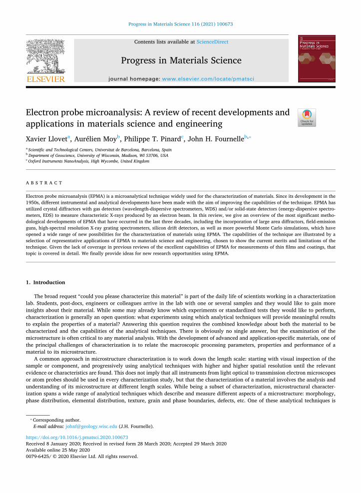
The impact of EPMA in materials science and engineering has been high. EPMA has proven to be a useful tool for the study of the microstructure and chemical composition of materials such as metals, alloys, steel, ceramics, glass, biomaterials, composites and advanced materials, to determine phase diagrams and phase transformations (Fig. 2), diffusion profiles, analysis of inclusions and precipitates, failure analysis, oxidation, corrosion and segregation phenomena and for the analysis of thin films and coatings.
As a review at the start of the 3rd decade of the 21st century, it is essential to note changes in technology and associated terminology. “In the beginning”, there were two distinct instruments: the electron microprobe (also known as electron probe mi-croanalyzer or electron microprobe analyzer) and the scanning electron microscope. And for most people, the electron probe mi-croanalyzer has meant WDS and additionally meant the analytical process also called EPMA, electron probe microanalysis (also referred to as electron probe X-ray microanalysis or electron microprobe analysis). Similarly, EDS was referring to the X-ray detector
1 The notations kV (kilovolt) and keV (kilo-electron volt) are used here in the strict sense: kV refers to an electrical potential (as between the cathode and anode of the beam source), whereas keV refers to an energy.
2 James Hillier [499] conceived of an electron probe microanalyzer in 1943, but his employer, the Radio Corporation of America, had no interest in pursuing this.
X. Llovet, et al. Progress in Materials Science 116 (2021) 100673
2
mounted upon an SEM. By the 3rd decade of the electron probe microanalyzer, in the 1980s, it was becoming more common to find EDS systems mounted upon electron probe microanalyzers. And only “old timers” today remember when the electron probe mi-croanalyzer only had a fixed beam; today electron probes are hybrids, they scan their beam as needed.
Also, by the 1980s there were rare sightings of WDS systems mounted upon SEMs (i.e., the Microspec WDS). Today, a rare electron probe microanalyzer does not have an EDS system, and in a few cases (with the hope this will increase) EDS is integrated with WDS in the automation and data processing for quantitative analysis; this has been the case for X-ray mapping for decades.
To avoid any confusion in this review, the term “electron probe microanalysis” and its abbreviation “EPMA” will always refer to the analytical technique defined by ISO [1], as the “technique of spatially-resolved elemental analysis based upon electron-excited X- ray spectrometry with a focussed electron probe and an electron interaction volume with micrometer to sub-micrometer dimensions”. EPMA can be performed using different electron microscopes (e.g., electron microprobes, scanning electron microscopes or trans-mission electron microscopes) and different X-ray spectrometers (e.g., WDS and/or EDS).
The aim of the present review article is to provide an overview of recent applications of EPMA to materials science and en-gineering as well as the most significant instrumental and methodological developments of the technique, since it has been two decades since the last comprehensive reviews were published [9,10]. Chapter 2 will start by reviewing the conventional principles and methods and continue by describing more specific application by EPMA, to conclude with discussion of new instrumentation. In chapter 3 some significant examples will be given. Most of the advances have been produced with the aim of extending the limits of
Fig. 1. (Left) Field emission SEM with SDD EDS and a WDS detector (courtesy of Dr. Stéphane Mathieu, University of Lorraine, France). (Right) Field emission electron probe with 5 WDS spectrometers and SDD EDS detector, also with RGA and plasma cleaner on airlock (University of Wisconsin- Madison, WI, USA).
Fig. 2. EPMA has been a critical tool for materials science since the early 1960s. Here is a plot of yearly publications where the terms electron probe and phase diagram were used.
X. Llovet, et al. Progress in Materials Science 116 (2021) 100673
3
EPMA towards higher spatial resolution, lower detection limits and improved analytical accuracy. Appendix A lists acronyms used in the text, Appendix B provides guidance for reporting EPMA results and experimental technique in material science and engineering papers, and Appendix C points out several potential issues affecting the accuracy of EPMA results.
2. Materials analysis by EPMA. Principles and conventional methods
2.1. Physical principles
EPMA uses bombardment of the specimen by a beam of monoenergetic electrons to produce characteristic X-rays from the specimen; due to the quantum nature of matter, there are discrete electron energy levels in each atom which upon excitation result in the emission of electromagnetic radiation (photons) at specific and discrete energy values within the soft and hard X-ray regions of the electromagnetic spectrum. These are characteristic of the atom’s identity and this fact is the basis of utility of EPMA for mi-croanalysis.
The detailed process by which characteristic X-rays are produced when a beam of electrons impinges on a target is as follows: the electrons interact repeatedly with the target atoms until they come to rest or exit from the surface. The possible interactions of electrons with atoms are elastic scattering, inelastic collisions and bremsstrahlung emission. Elastic interactions are those in which the direction of movement of the electrons change but the initial and final electronic states of the target atom remain essentially unchanged (the ground state). By contrast, inelastic interactions are those in which the target atom is brought to an excited state, which means that part of the electron’s kinetic energy is taken up by the atomic electrons. There are several types of inelastic collisions, which include excitation of electrons in the conduction or valence bands, excitation of plasmons and ionization of inner shells (i.e., the production of a vacancy in an inner shell).
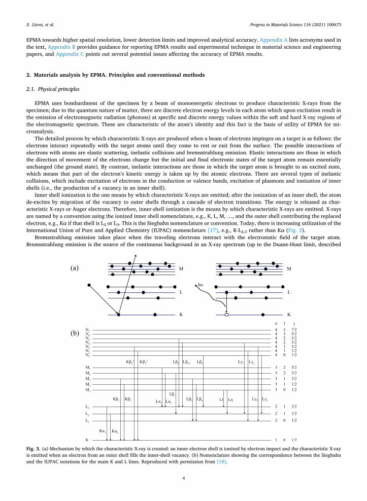
Inner shell ionization is the one means by which characteristic X-rays are emitted; after the ionization of an inner shell, the atom de-excites by migration of the vacancy to outer shells through a cascade of electron transitions. The energy is released as char-acteristic X-rays or Auger electrons. Therefore, inner-shell ionization is the means by which characteristic X-rays are emitted. X-rays are named by a convention using the ionized inner shell nomenclature, e.g., K, L, M, …, and the outer shell contributing the replaced electron, e.g., Kα if that shell is L2 or L3. This is the Siegbahn nomenclature or convention. Today, there is increasing utilization of the International Union of Pure and Applied Chemistry (IUPAC) nomenclature [17], e.g., K-L2,3 rather than Kα (Fig. 3).
Bremsstrahlung emission takes place when the traveling electrons interact with the electrostatic field of the target atom. Bremsstrahlung emission is the source of the continuous background in an X-ray spectrum (up to the Duane-Hunt limit, described
Fig. 3. (a) Mechanism by which the characteristic X-ray is created: an inner electron shell is ionized by electron impact and the characteristic X-ray is emitted when an electron from an outer shell fills the inner-shell vacancy. (b) Nomenclature showing the correspondence between the Siegbahn and the IUPAC notations for the main K and L lines. Reproduced with permission from [18].
X. Llovet, et al. Progress in Materials Science 116 (2021) 100673
4
later) and it is thus the limiting factor for trace element detection (see Section 2.8) Generation of characteristic X-rays and bremsstrahlung X-rays is not constant with depth, but rather follows a certain distribution,
which is known as the z( ) function (see Section 2.3.1). Before emerging from the specimen surface, both characteristic X-rays and bremsstrahlung photons may interact with the sample atoms mainly through photoelectric absorption. The photon is then absorbed by the atom and an atomic electron is ejected; the atom de-excites by migration of the vacancy to an outer shell with the subsequent emission of characteristic (fluorescent) X-rays or Auger electrons. Because the mean free path of X-rays with energies of several keV is much larger than the range of keV electrons, fluorescence is generated from a large distance from the electron point of impact, giving rise to potential errors of secondary or boundary fluorescence (see Section 2.5.2).
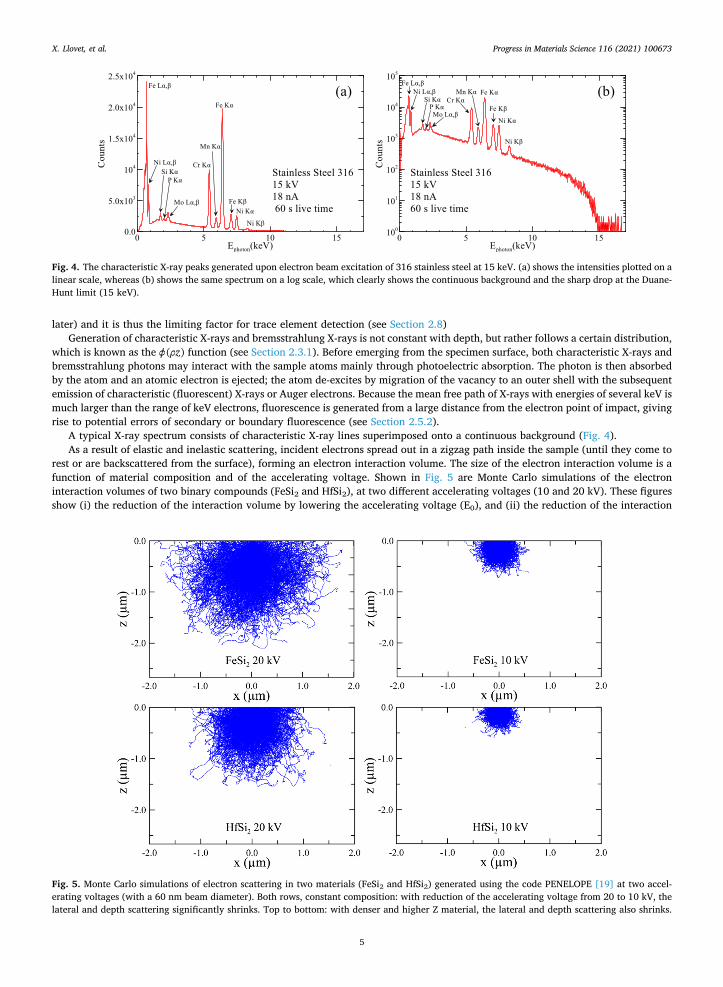
A typical X-ray spectrum consists of characteristic X-ray lines superimposed onto a continuous background (Fig. 4). As a result of elastic and inelastic scattering, incident electrons spread out in a zigzag path inside the sample (until they come to
rest or are backscattered from the surface), forming an electron interaction volume. The size of the electron interaction volume is a function of material composition and of the accelerating voltage. Shown in Fig. 5 are Monte Carlo simulations of the electron interaction volumes of two binary compounds (FeSi2 and HfSi2), at two different accelerating voltages (10 and 20 kV). These figures show (i) the reduction of the interaction volume by lowering the accelerating voltage (E0), and (ii) the reduction of the interaction
Fig. 4. The characteristic X-ray peaks generated upon electron beam excitation of 316 stainless steel at 15 keV. (a) shows the intensities plotted on a linear scale, whereas (b) shows the same spectrum on a log scale, which clearly shows the continuous background and the sharp drop at the Duane- Hunt limit (15 keV).
Fig. 5. Monte Carlo simulations of electron scattering in two materials (FeSi2 and HfSi2) generated using the code PENELOPE [19] at two accel-erating voltages (with a 60 nm beam diameter). Both rows, constant composition: with reduction of the accelerating voltage from 20 to 10 kV, the lateral and depth scattering significantly shrinks. Top to bottom: with denser and higher Z material, the lateral and depth scattering also shrinks.
X. Llovet, et al. Progress in Materials Science 116 (2021) 100673
5
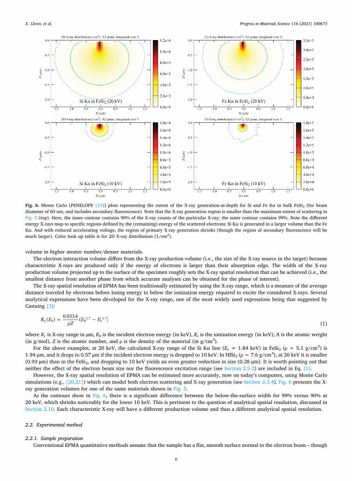
volume in higher atomic number/denser materials. The electron interaction volume differs from the X-ray production volume (i.e., the size of the X-ray source in the target) because
characteristic X-rays are produced only if the energy of electrons is larger than their absorption edge. The width of the X-ray production volume projected up to the surface of the specimen roughly sets the X-ray spatial resolution that can be achieved (i.e., the smallest distance from another phase from which accurate analyses can be obtained for the phase of interest).
The X-ray spatial resolution of EPMA has been traditionally estimated by using the X-ray range, which is a measure of the average distance traveled by electrons before losing energy to below the ionization energy required to excite the considered X-rays. Several analytical expressions have been developed for the X-ray range, one of the most widely used expressions being that suggested by Castaing [3]:
=R E AZ
E E( ) 0.033 ( )x 0 01.7
c1.7
(1)
where Rx is X-ray range in µm, E0 is the incident electron energy (in keV), Ec is the ionization energy (in keV), A is the atomic weight (in g/mol), Z is the atomic number, and ρ is the density of the material (in g/cm3).
For the above examples, at 20 keV, the calculated X-ray range of the Si Kα line (Ec = 1.84 keV) in FeSi2 (ρ = 5.1 g/cm3) is 1.94 μm, and it drops to 0.57 μm if the incident electron energy is dropped to 10 keV. In HfSi2 (ρ = 7.6 g/cm3), at 20 keV it is smaller (0.93 μm) than in the FeSi2, and dropping to 10 keV yields an even greater reduction in size (0.28 μm). It is worth pointing out that neither the effect of the electron beam size nor the fluorescence excitation range (see Section 2.5.2) are included in Eq. (1).
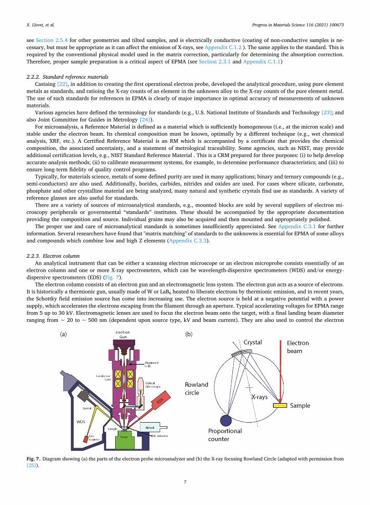
However, the X-ray spatial resolution of EPMA can be estimated more accurately, now on today’s computers, using Monte Carlo simulations (e.g., [20,21]) which can model both electron scattering and X-ray generation (see Section 2.3.4). Fig. 6 presents the X- ray generation volumes for one of the same materials shown in Fig. 5.
As the contours show in Fig. 6, there is a significant difference between the below-the-surface width for 99% versus 90% at 20 keV, which shrinks noticeably for the lower 10 keV. This is pertinent to the question of analytical spatial resolution, discussed in Section 2.10. Each characteristic X-ray will have a different production volume and thus a different analytical spatial resolution.
2.2. Experimental method
2.2.1. Sample preparation Conventional EPMA quantitative methods assume that the sample has a flat, smooth surface normal to the electron beam – though
Fig. 6. Monte Carlo (PENELOPE [19]) plots representing the extent of the X-ray generation-at-depth for Si and Fe Kα in bulk FeSi2 (for beam diameter of 60 nm, and includes secondary fluorescence). Note that the X-ray generation region is smaller than the maximum extent of scattering in Fig. 5 (top). Here, the inner contour contains 90% of the X-ray counts of the particular X-ray; the outer contour contains 99%. Note the different energy X-rays map to specific regions defined by the (remaining) energy of the scattered electrons; Si Kα is generated in a larger volume than the Fe Kα. And with reduced accelerating voltage, the region of primary X-ray generation shrinks (though the region of secondary fluorescence will be much larger). Color look up table is for 2D X-ray distribution (1/cm2).
X. Llovet, et al. Progress in Materials Science 116 (2021) 100673
6
see Section 2.5.4 for other geometries and tilted samples, and is electrically conductive (coating of non-conductive samples is ne-cessary, but must be appropriate as it can affect the emission of X-rays, see Appendix C.1.2 ). The same applies to the standard. This is required by the conventional physical model used in the matrix correction, particularly for determining the absorption correction. Therefore, proper sample preparation is a critical aspect of EPMA (see Section 2.3.1 and Appendix C.1.1)
2.2.2. Standard reference materials Castaing [22], in addition to creating the first operational electron probe, developed the analytical procedure, using pure element
metals as standards, and ratioing the X-ray counts of an element in the unknown alloy to the X-ray counts of the pure element metal. The use of such standards for references in EPMA is clearly of major importance in optimal accuracy of measurements of unknown materials.
Various agencies have defined the terminology for standards (e.g., U.S. National Institute of Standards and Technology [23]; and also Joint Committee for Guides in Metrology [24]).
For microanalysis, a Reference Material is defined as a material which is sufficiently homogeneous (i.e., at the micron scale) and stable under the electron beam. Its chemical composition must be known, optimally by a different technique (e.g., wet chemical analysis, XRF, etc.). A Certified Reference Material is an RM which is accompanied by a certificate that provides the chemical composition, the associated uncertainty, and a statement of metrological traceability. Some agencies, such as NIST, may provide additional certification levels, e.g., NIST Standard Reference Material . This is a CRM prepared for three purposes: (i) to help develop accurate analysis methods; (ii) to calibrate measurement systems, for example, to determine performance characteristics; and (iii) to ensure long-term fidelity of quality control programs.
Typically, for materials science, metals of some defined purity are used in many applications; binary and ternary compounds (e.g., semi-conductors) are also used. Additionally, borides, carbides, nitrides and oxides are used. For cases where silicate, carbonate, phosphate and other crystalline material are being analyzed, many natural and synthetic crystals find use as standards. A variety of reference glasses are also useful for standards.
There are a variety of sources of microanalytical standards, e.g., mounted blocks are sold by several suppliers of electron mi-croscopy peripherals or governmental “standards” institutes. These should be accompanied by the appropriate documentation providing the composition and source. Individual grains may also be acquired and then mounted and appropriately polished.
The proper use and care of microanalytical standards is sometimes insufficiently appreciated. See Appendix C.3.1 for further information. Several researchers have found that "matrix matching" of standards to the unknowns is essential for EPMA of some alloys and compounds which combine low and high Z elements (Appendix C.3.3).
2.2.3. Electron column An analytical instrument that can be either a scanning electron microscope or an electron microprobe consists essentially of an
electron column and one or more X-ray spectrometers, which can be wavelength-dispersive spectrometers (WDS) and/or energy- dispersive spectrometers (EDS) (Fig. 7).
The electron column consists of an electron gun and an electromagnetic lens system. The electron gun acts as a source of electrons. It is historically a thermionic gun, usually made of W or LaB6 heated to liberate electrons by thermionic emission, and in recent years, the Schottky field emission source has come into increasing use. The electron source is held at a negative potential with a power supply, which accelerates the electrons escaping from the filament through an aperture. Typical accelerating voltages for EPMA range from 5 up to 30 kV. Electromagnetic lenses are used to focus the electron beam onto the target, with a final landing beam diameter ranging from ~ 20 to ~ 500 nm (dependent upon source type, kV and beam current). They are also used to control the electron
Fig. 7. Diagram showing (a) the parts of the electron probe microanalyzer and (b) the X-ray focusing Rowland Circle (adapted with permission from [25]).
X. Llovet, et al. Progress in Materials Science 116 (2021) 100673
7
current, i.e., the number of incoming electrons per unit time, with possible values in the range 100 pA to 10 μA, typically in the range of 1 – 500nA depending upon applications, materials and spectrometers, e.g., EDS vs WDS. The electron current is measured with a Faraday cup and may be stabilized by means of a beam regulation device. The sample is connected to ground to ensure electron conductivity; if the sample is not itself electrically conductive, a thin conductive coating (e.g., carbon, not gold, see Appendix C.1.2) is applied.
Conventional high vacuum technology (e.g., 10-7 mbar) is used so as to prevent oxidation of the electron source, high voltage arcing in the gun and scattering of the electrons in the beam by the residual gas. The beam can be scanned and electron images collected, most commonly by a backscattered electron detector. Secondary electron images may be useful also, particularly to assist in clarifying any 3-dimensional features (e.g., holes). Absorbed current images may also provide interesting information in some ma-terials.
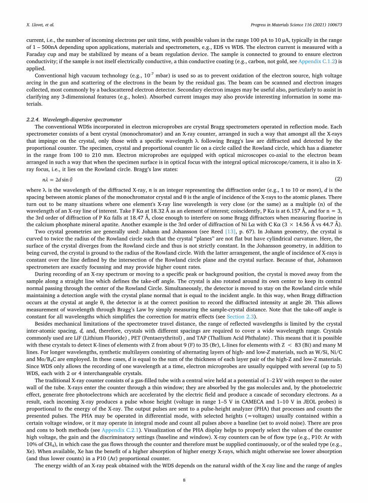
2.2.4. Wavelength-dispersive spectrometer The conventional WDSs incorporated in electron microprobes are crystal Bragg spectrometers operated in reflection mode. Each
spectrometer consists of a bent crystal (monochromator) and an X-ray counter, arranged in such a way that amongst all the X-rays that impinge on the crystal, only those with a specific wavelength λ following Bragg's law are diffracted and detected by the proportional counter. The specimen, crystal and proportional counter lie on a circle called the Rowland circle, which has a diameter in the range from 100 to 210 mm. Electron microprobes are equipped with optical microscopes co-axial to the electron beam arranged in such a way that when the specimen surface is in optical focus with the integral optical microscope/camera, it is also in X- ray focus, i.e., it lies on the Rowland circle. Bragg’s law states:
=n d2 sin (2)
where λ is the wavelength of the diffracted X-ray, n is an integer representing the diffraction order (e.g., 1 to 10 or more), d is the spacing between atomic planes of the monochromator crystal and θ is the angle of incidence of the X-rays to the atomic planes. There turn out to be many situations where one element's X-ray line wavelength is very close (or the same) as a multiple (n) of the wavelength of an X-ray line of interest. Take F Kα at 18.32 Å as an element of interest; coincidently, P Kα is at 6.157 Å, and for n = 3, the 3rd order of diffraction of P Kα falls at 18.47 Å, close enough to interfere on some Bragg diffractors when measuring fluorine in the calcium phosphate mineral apatite. Another example is the 3rd order of diffraction of Ni Lα with C Kα (3 × 14.56 Å vs 44.7 Å).
Two crystal geometries are generally used: Johann and Johansson (see Reed [13], p. 67). In Johann geometry, the crystal is curved to twice the radius of the Rowland circle such that the crystal “planes” are not flat but have cylindrical curvature. Here, the surface of the crystal diverges from the Rowland circle and thus is not strictly constant. In the Johansson geometry, in addition to being curved, the crystal is ground to the radius of the Rowland circle. With the latter arrangement, the angle of incidence of X-rays is constant over the line defined by the intersection of the Rowland circle plane and the crystal surface. Because of that, Johansson spectrometers are exactly focussing and may provide higher count rates.
During recording of an X-ray spectrum or moving to a specific peak or background position, the crystal is moved away from the sample along a straight line which defines the take-off angle. The crystal is also rotated around its own center to keep its central normal passing through the center of the Rowland Circle. Simultaneously, the detector is moved to stay on the Rowland circle while maintaining a detection angle with the crystal plane normal that is equal to the incident angle. In this way, when Bragg diffraction occurs at the crystal at angle θ, the detector is at the correct position to record the diffracted intensity at angle 2θ. This allows measurement of wavelength through Bragg’s Law by simply measuring the sample-crystal distance. Note that the take-off angle is constant for all wavelengths which simplifies the correction for matrix effects (see Section 2.3).
Besides mechanical limitations of the spectrometer travel distance, the range of reflected wavelengths is limited by the crystal inter-atomic spacing, d, and, therefore, crystals with different spacings are required to cover a wide wavelength range. Crystals commonly used are LiF (Lithium Fluoride) , PET (Pentaerythritol) , and TAP (Thallium Acid Phthalate) . This means that it is possible with these crystals to detect K-lines of elements with Z from about 9 (F) to 35 (Br), L-lines for elements with Z < 83 (Bi) and many M lines. For longer wavelengths, synthetic multilayers consisting of alternating layers of high- and low-Z materials, such as W/Si, Ni/C and Mo/B4C are employed. In these cases, d is equal to the sum of the thickness of each layer pair of the high-Z and low-Z materials. Since WDS only allows the recording of one wavelength at a time, electron microprobes are usually equipped with several (up to 5) WDS, each with 2 or 4 interchangeable crystals.
The traditional X-ray counter consists of a gas-filled tube with a central wire held at a potential of 1–2 kV with respect to the outer wall of the tube. X-rays enter the counter through a thin window; they are absorbed by the gas molecules and, by the photoelectric effect, generate free photoelectrons which are accelerated by the electric field and produce a cascade of secondary electrons. As a result, each incoming X-ray produces a pulse whose height (voltage in range 1–5 V in CAMECA and 1–10 V in JEOL probes) is proportional to the energy of the X-ray. The output pulses are sent to a pulse-height analyzer (PHA) that processes and counts the presented pulses. The PHA may be operated in differential mode, with selected heights (=voltages) usually contained within a certain voltage window, or it may operate in integral mode and count all pulses above a baseline (set to avoid noise). There are pros and cons to both methods (see Appendix C.2.1). Visualization of the PHA display helps to properly select the values of the counter high voltage, the gain and the discriminatory settings (baseline and window). X-ray counters can be of flow type (e.g., P10: Ar with 10% of CH4), in which case the gas flows through the counter and therefore must be supplied continuously, or of the sealed type (e.g., Xe). When available, Xe has the benefit of a higher absorption of higher energy X-rays, which might otherwise see lower absorption (and thus lower counts) in a P10 (Ar) proportional counter.
The energy width of an X-ray peak obtained with the WDS depends on the natural width of the X-ray line and the range of angles
X. Llovet, et al. Progress in Materials Science 116 (2021) 100673
8
for which Bragg reflection occurs on the crystal. This depends on the geometrical arrangement of the spectrometer, and the width of the intrinsic reflection curve of the crystal. Typical peak widths are in the range ~ 2–8 eV for a TAP crystal, ~ 4–60 eV for PET crystal and ~ 12–80 eV for an LiF crystal. The recording of a diffraction peak may be realized by scanning the WDS, either discretely, one channel at a time, or by slowly moving the spectrometer motor.
Optimally, one would want to collect the total signal of each peak by integrating all of the channels under the peak. For WDS, this would entail a scanning of the spectrometer in angle and is generally too slow for rapid quantitative data acquisition or X-ray mapping. Thus, a single wide channel centered on the peak, is counted, and assumed to be representative of the total area under the wider peak (though see Appendix C.2.4 for chemical peak shifts of some X-ray lines ).
The standard procedure to obtain the net peak intensity in a WDS measurement is to record the counting rate at the channel corresponding to the center/maximum of the peak, and usually but not always at two background positions at both sides of the peak (it is permissible to use only one side if conditions require it and it is possible to “model the background” properly that way). Background intensity at the peak maximum energy is then obtained by interpolation of the background measurements (see Appendix C.2.5). Optimally the software permits different background model options ranging from linear, to curved/exponential, to sloping, which is subtracted from the measured counting rate. This procedure gives, in general, accurate results because of the high peak-to- background ratio of WDS spectra.
Higher order reflections ( >n 1) in Bragg’s law must not be ignored since they potentially are a source of spectral interference (Appendix C.2.3). They can produce critical problems for trace element work. In general, it is possible to minimize the influence of high-order diffraction peaks up to ~ 90% by properly setting an energy window in the PHA, although this cannot be counted on for 100% suppression. However, inadvertent pulse height suppression of n = 1 peaks must be avoided (Appendix C.2.1 ).
Deadtime must be corrected: as it takes the electronics a finite time (on the order of microsecond) to process an event (detecting a pulse generated by an X-ray), there is a period when it is “busy” with one signal and must ignore others. The detector is thus blind to arrival of new photons during this “deadtime.” When the X-ray signal rate is low, it is unlikely that a second photon will arrive during the “busy” time. When the signal rate is high, a significant fraction of real time is spent processing events and this fraction of real time is reported as the deadtime. Measured counts are corrected for deadtime by the software (though see Appendix C.2.2 ).
There are at least two new “non-traditional” WDS detectors, and they are introduced in Section 2.12.
2.2.5. Energy-dispersive spectrometer EDS is today the most widely used microanalytical technique in materials science for several reasons: (i) ED spectrometers can be
installed on almost any SEM, (ii) all elements in the periodic table except H and He can be detected in parallel, (iii) EDS can quickly identify and quantify the elements located in specific regions of a sample with minimal preparation and instruction. It is a readily available technique, and the cost of an SEM with ED spectrometer is a fraction of the cost of an electron microprobe.
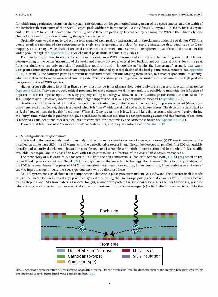
The technology of EDS drastically changed in 1996 with the first commercial silicon drift detector (SDD, Fig. 8) [26] based on the groundbreaking work of Gatti and Rehak [27]. In comparison to the preceding technology, the lithium-drifted silicon crystal detector, the SDD improves almost all aspects of EDS X-ray detection: better energy resolution, higher count rate, larger active area and ease of use (no liquid nitrogen). Only the SDD type detectors will be discussed here.
An EDS system consists of three main components: a detector, a pulse processor and analysis software. The detector itself is made of (i) a collimator to block stray X-rays produced by electrons hitting the microscope pole piece and chamber walls, (ii) an electron trap to stop SEs and BSEs from entering the detector, (iii) a window to protect the sensor and serve as a vacuum barrier, (iv) a sensor where X-rays are converted into an electrical current proportional to the X-ray energy, (v) a field effect transistor to amplify the
Fig. 8. Schematic representation of cross section of anSDD detector. Dashed arrows indicate the drift direction of the electron-hole pairs created by two incoming X-rays. Reproduced with permission from [28].
X. Llovet, et al. Progress in Materials Science 116 (2021) 100673
9
signal, (vi) a Peltier element to cool the sensor to reduce electrical noise and (vii) a heat sink to dissipate the heat produced by the Peltier element [16].
As an incoming X-ray travels or “disperses” through the sensor, it is progressively absorbed as it interacts with the valence electrons of the silicon atoms, which jump to the conduction band. The energy of each incoming X-ray is therefore converted into a proportional number of electron-hole pairs. By applying different voltages across the sensor, the electrons then “drift” towards the anode where their charge is converted to a voltage signal by the field effect transistor. By measuring each jump in the voltage signal (“the ramp”), the pulse processor detects X-rays and determines their energy. If the voltage jumps of two or more X-rays arriving closely spaced in time are not well-separated, the pulse processor rejects these events as it cannot accurately determine their energy [15,16]. Indeed, if the two X-rays arrive simultaneously, they cannot be rejected, and a “sum” peak is recorded. Finally, the analysis software accumulates the number of X-ray counts in each energy bin of the spectrum and may perform some correction to eliminate artifacts such as Si escape peaks originating from a loss of charge due to the emission of a Si X-ray out of the sensor [29,30] and sum peaks originating from coincident X-rays that could not be rejected by the pulse processor [31-34].
EDS has less energy resolution than WDS which means that overlaps between some X-ray lines are more common (e.g., V Kα by Ti Kβ, Mn Kα by Cr Kβ). Peak deconvolution is often necessary in order to extract X-ray intensities. This is normally performed using either theoretical or experimental peak profiles which are fitted to the unknown experimental spectrum using a least-squares ap-proach [35-37]. Ritchie et al. [36] showed that this strategy can accurately resolve strong overlapping X-ray lines like Ba L and Ti K. The poorer energy resolution of EDS (relative to WDS) also limits its ability to detect elements present in low concentrations due to its lower peak-to-background ratio. While EDS has been used to measure minor (< 10 wt%) and trace (< 1 wt%) concentrations [38], it is becoming more common to see EDS being used in combination with WDS [39,40], both in SEMs and in electron probes. The energy resolution of the EDS is commonly specified as FWHM of the Mn Kα peak at a given input count rate (note that the ISO specification 15632:2012 [41] indicates that the FWHM of the C Kα peak should also be specified, in case detection of X-rays lower than 1 keV is specified).
As an EDS spectrum may contain several peaks, including several peaks from the same element, a common feature of the analysis software is to automatically identify the elements. Newbury [42] reported several misidentification issues with the automatic identification routine in some software and recommended that a manual verification should always be performed. He also expressed warnings about the quantification results obtained by some EDS systems [43,44]. While there is no fundamental difference between EDS and WDS quantification, some advantages of EDS such as its ease of use and its availability in many laboratories often result in inexperienced users, with no training in recognizing problems, generating incorrect analytical data. The normalization of the EDS analytical output to 100 wt% can be identified as a prime cause for concern, as the unnormalized “analytical total” is an important indication that the results are accurate (see Appendix C.4.1), or that they have a problem which needs attention (e.g., secondary fluorescence, see Section 2.5.2).
2.3. Quantitative methods
With Castaing’s pioneering development of the electron probe microanalyzer instrument, he also laid the basis for quantitative analysis in two essential ways. First, he recognized that with this technique, it was essential to measure X-ray intensities of a standard reference material, using the exact same equipment and analytical conditions as used for measuring the unknown material. He then generated a “k-ratio”, dividing the measured X-ray intensity of the unknown by that of the standard (“Castaing’s First Approximation”), which approximates the elemental concentration of the studied element in the unknown (when pure element standards are used). Next, he proposed two methods for correcting this k-ratio, to account for the so-called matrix effects, and to accurately determine the elemental composition of the unknown. One method utilized an empirical ‘alpha factor’ correction for binary compounds, where each pair of elements has a pair of constant α-factors representing the effect that each element has upon the other for measured X-ray intensity. These hyperbolic curves are created from experimentally created compounds together with the pure end member compositions. Castaing also proposed a more theoretical, physics-based quantitative analysis method, to ac-count for both absorption (A) of generated X-rays as well as fluorescence (F) effects. This approach, which would become known as the ZAF correction technique, was further developed in the 1960 s and 1970 s with addition of a “Z” (atomic number) effect [45]. This approach was then refined into a second generation of physical parameter-based matrix correction procedures, focused upon the use of the depth-distribution of ionizations or z( ) function. The development of the z( ) matrix correction procedures was mainly performed in the 1980's and in the beginning of the 1990's, almost ceasing from the 2000’s on. A key reason was to improve EPMA of the lower energy “light elements” and that of thin films, which was successful; these z( )-based matrix corrections also worked well for all elements. A detailed review of these “second-generation” matrix correction procedures is in Lavrent’ev et al. [46].
2.3.1. Matrix corrections The starting point of a quantitative method is to establish the relation between X-ray intensity and element concentration. This
can be done by modelling electrons entering the material and then having them interact in physically predictable ways. For this, there are essentially two different approaches: (i) integrating every contribution along the electron trajectory and taking into account the X- ray generation loss due to electron backscattering, and (ii) integrating every contribution along the sample depth, provided the depth- distribution of X-ray emission is known. The first approach is the basis of the ZAF methods while the second approach is that used in the z( ) methods. While ZAF corrections are still available on some systems, there is an overall trend to replace them with the more
X. Llovet, et al. Progress in Materials Science 116 (2021) 100673
10
advanced z( ) corrections3. As already pointed out, both ZAF and z( ) methods make several assumptions about the sample, namely that (i) it is stable under
the impact of the electron beam, (ii) it is chemically homogeneous over the analysis volume, (iii) it is electrically conductive and (iv) it has a flat surface normal to the electron beam.
In the ZAF methods, the X-ray intensity Ii emitted by element i is written as:
= + + +I n NA
c T R S f f f4
(1 ) (1/ ) ( )(1 )ii
i jkelA
CK c b (3)
where nel is the number of incident electrons, is the intrinsic detector efficiency, /4 is the solid angle of collection, ci is the weight fraction of element i,NA is Avogadro’s number, Ai is the atomic weight of element i, jk is the partial fluorescence yield, + T(1 )CK is the enhancement factor due to Coster-Kronig transitions, R is the backscattering factor, f(χ) is the absorption factor with χ = csc(ψ) and ψ being the X-ray take-off angle, 1/S is the stopping power factor (also called deceleration factor), and fc and fb are the characteristic and continuum (Bremsstrahlung) fluorescence factors, respectively.
The partial fluorescence yield is given by =jk j jk, where j is the fluorescence yield of shell j and jk is the radiative transition probability for an electron jumping from shell k to shell j, also known as line fraction [13]. For L, M and N-subshells, the + T(1 )CKfactor accounts for the increase of X-rays due to Coster-Kronig transitions from vacancies produced in other sub-shells.
The backscattering factor R accounts for the loss of X-ray intensity due to backscattered electrons, the absorption factor f(χ) corrects for those X-rays that were generated in the sample but could not escape from it, and the fluorescence factor + +f f(1 )c baccounts for those X-rays that were not generated by primary electron impact but from fluorescence by primary characteristic X-rays and of bremsstrahlung photons. Different analytical expressions to calculate the backscattering, deceleration, absorption and fluorescence factors have been developed over the years (see e.g., Scott et al. [14]).
Because Eq. (3) contains instrumental parameters (n , ,el 4 ) and atomic parameters ( + T(1 )jk, CK ), which may not be well known, the X-ray intensity is normalized to that emitted from a reference standard that contains the element of interest, measured under the same instrumental conditions. By doing so, the ratio of X-ray intensities or k-ratio, ki, is given by:
= = × ×+ +
+ +k I
Ic
cR S
R Sf
ff f
f f/
( / )( )
( )(1 )
(1 )ii
i
i
istd std std std
c b
c bstd (4)
where the superscript “std” denotes that the corresponding quantity is evaluated in the standard. Equation (4) can be written in a compact form as:
= =k II
cc
ZAFii
i
i
istd std (5)
where Z corresponds to the atomic number correction factor, A is the absorption correction factor and F is the fluorescence correction factor. The absorption correction is often the most significant correction, especially for the analysis of light elements. This effect can be minimized by selecting a lower accelerating voltage but sufficient overvoltage U (where U = E0/Ec, as terms defined in Eq. (1)) that yields a shorter absorption path length in the sample and thus a maximum X-ray intensity for the element of interest. The factor Z corrects for differences in electron transport and X-ray generation between unknown and standard. The fluorescence factor F is usually the least significant of the three correction factors. Note that by using composition matching standards, the different cor-rection factors may be reduced (e.g., Appendix C.3.3).
In the z( ) methods, the relationship between the concentration ci of element i in the sample and the number of emitted X-rays, Ii, is written as:
= + × + +I n NA
c T E z µ z csc d z f f4
(1 ) ( ) ( ) exp ( ) (1 )ii
i jk j jelA
CK 0 0 c b (6)
where E( )j 0 is the ionization cross section of shell j for electrons with incident energy E0, z( )j is the depth-distribution of ioni-zations of shell j of element i and µ/ is the MAC (mass attenuation/absorption coefficient), where is the sample density.
A number of analytical parameterizations of the z( ) function have been developed over the years, which are defined by a few parameters that generally depend on E0, Z, and the ionization energy Ec. These parameters have been computed from physical quantities and/or fits to experimental or Monte Carlo simulation data. The z( ) parameterizations usually employ quadrilateral, Gaussian, parabolic or exponential functions, which can be analytically integrated to solve Eq. (6). Examples of z( ) functions, as shown in Fig. 9, can be found in Reed [13] and in Lavrent’ev et al. [46].
The k-ratio can be written as:
= = ×+ +
+ +( )( )
k II
c z z d z
c z z d z
f ff f
( ) exp csc( )
( ) exp csc( )
(1 )(1 )i
i
i
i jµ
i jµstd
0
std0
std stdc b
c bstd
(7)
3 One must be aware that sometimes something called “ZAF” really is shorthand for the term matrix correction, which might actually be a z( )correction.
X. Llovet, et al. Progress in Materials Science 116 (2021) 100673
11
where again superscript “std” denotes that the corresponding quantity is evaluated in the standard. Equation (7) can be written in a compact form as:
= =k II
cc
ZA[ ]Fii
i
i
istd std (8)
where [ZA] corresponds now to the combined correction factor of atomic number and absorption as calculated with the z( )function, while F is the fluorescence correction factor.
In both the ZAF and z( ) methods, k-ratios are measured for all elements that make up the sample (except for those estimated by stoichiometry or by other means) and the resulting system of equations is solved by using an iterative procedure. This is required since several quantities that occur in Eqs. (4) and (7) depend themselves on the unknown concentrations. In general, convergence is quickly achieved using simple iterative procedures [14].
A key parameter for the absorption correction in both ZAF and z( ) methods is the mass attenuation or absorption coefficient, the MAC. Different MAC tabulations are available in the literature, which are based on a limited number of measured values, with theoretical calculations and, significantly, extrapolations across the atomic number Z range. Commonly used MACs tabulations are those of Heinrich [48], Henke et al. [49] or the most recent database FFAST from Chantler et al. [50], although “light element” MACS have received critical attention (see Section 2.6). In the case of compounds, the accepted convention is that the MAC is calculated by using the MAC of the pure element weighted by the mass fraction of the element in the compound.
As a result of the extensive research performed over the years, a large number of ZAF and z( ) methods exist, which include different combinations of physical parameters. Sometimes users of EPMA may not be aware of the significance of the choices (see Appendix C.3.2).
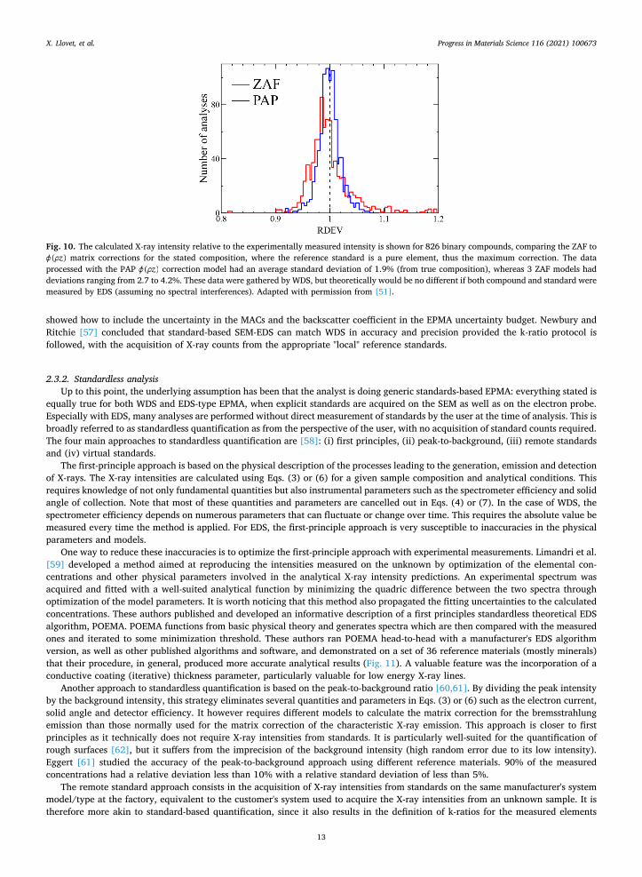
Correction procedures have been generally assessed by comparing calculated k-ratios with measured values, taken from large databases of measurements on samples of known composition. The spread and mean value of the histogram of the ratio kcal/kexp, where kcal is the calculated value by a particular matrix correction and kexp is the measured k-ratio, is used to assess the performance of the procedure under investigation. Histograms of kcal/kexp have been published for most of the available correction methods and have shown that z( ) methods can provide generally more accurate values compared with ZAF methods (Fig. 10). For this reason, ZAF methods have generally been replaced by z( ) methods, especially–but not only– for the analysis of light elements.
EPMA concentrations flow from a k-ratio value, which typically results from several X-ray intensity measurements (for the unknown, a peak intensity and two background intensity measurements, and likewise for the standard). All of these measurements are subject to a range of random and systematic errors, which will impact the accuracy of the analytical results [52]. Generally, only the precision portion of the uncertainty budget arising from counting statistics has been considered, which may represent only a small fraction of the accuracy uncertainty. X-ray counting statistics follow a Poisson distribution, for which the standard deviation is defined as the square root of acquired counts. The precision from counting statistics depends essentially on the number of counts recorded in each individual measurement, where greater precision comes from a greater accumulation of counts. The standard deviation of the measured k-ratio can then be obtained by combining the standard deviation of each individual X-ray measurement using conventional propagation of error rules (e.g., Scott et al. [14]). Evaluations of the statistics of the X-ray intensity measurements are detailed in various publications. Ancey et al. [53] applied a rigorous treatment of Poisson counting statistics, using the chi- squared test, to derive the confidence interval of the measured k-ratio, for a chosen confidence level (e.g., 95% or 99%). Lifshin et al. [54] went further and derived the confidence interval of the evaluated concentration by using an equation derived by Ziebold [52]. More recently, Marinenko and Leigh [55] showed how to apply the ISO/GUM guide for the evaluation of the measurement un-certainties in EPMA quantification, using Lifshin et al.’s approach to include matrix correction errors. Ritchie and Newbury [56]
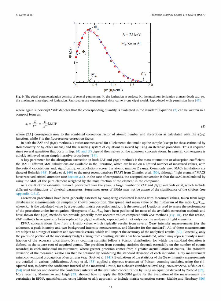
Fig. 9. The z( ) parameterization consists of several parameters: 0 the ionization at surface; m the maximum ionization at mass-depth zm; z xthe maximum mass-depth of ionization. Red squares are experimental data; curve is one ϕ(ρz) model. Reproduced wtih permission from [47].
X. Llovet, et al. Progress in Materials Science 116 (2021) 100673
12
showed how to include the uncertainty in the MACs and the backscatter coefficient in the EPMA uncertainty budget. Newbury and Ritchie [57] concluded that standard-based SEM-EDS can match WDS in accuracy and precision provided the k-ratio protocol is followed, with the acquisition of X-ray counts from the appropriate "local" reference standards.
2.3.2. Standardless analysis Up to this point, the underlying assumption has been that the analyst is doing generic standards-based EPMA: everything stated is
equally true for both WDS and EDS-type EPMA, when explicit standards are acquired on the SEM as well as on the electron probe. Especially with EDS, many analyses are performed without direct measurement of standards by the user at the time of analysis. This is broadly referred to as standardless quantification as from the perspective of the user, with no acquisition of standard counts required. The four main approaches to standardless quantification are [58]: (i) first principles, (ii) peak-to-background, (iii) remote standards and (iv) virtual standards.
The first-principle approach is based on the physical description of the processes leading to the generation, emission and detection of X-rays. The X-ray intensities are calculated using Eqs. (3) or (6) for a given sample composition and analytical conditions. This requires knowledge of not only fundamental quantities but also instrumental parameters such as the spectrometer efficiency and solid angle of collection. Note that most of these quantities and parameters are cancelled out in Eqs. (4) or (7). In the case of WDS, the spectrometer efficiency depends on numerous parameters that can fluctuate or change over time. This requires the absolute value be measured every time the method is applied. For EDS, the first-principle approach is very susceptible to inaccuracies in the physical parameters and models.
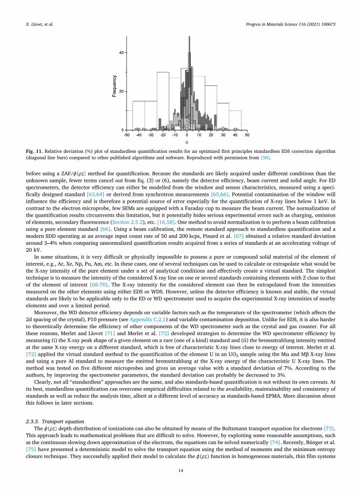
One way to reduce these inaccuracies is to optimize the first-principle approach with experimental measurements. Limandri et al. [59] developed a method aimed at reproducing the intensities measured on the unknown by optimization of the elemental con-centrations and other physical parameters involved in the analytical X-ray intensity predictions. An experimental spectrum was acquired and fitted with a well-suited analytical function by minimizing the quadric difference between the two spectra through optimization of the model parameters. It is worth noticing that this method also propagated the fitting uncertainties to the calculated concentrations. These authors published and developed an informative description of a first principles standardless theoretical EDS algorithm, POEMA. POEMA functions from basic physical theory and generates spectra which are then compared with the measured ones and iterated to some minimization threshold. These authors ran POEMA head-to-head with a manufacturer's EDS algorithm version, as well as other published algorithms and software, and demonstrated on a set of 36 reference materials (mostly minerals) that their procedure, in general, produced more accurate analytical results (Fig. 11). A valuable feature was the incorporation of a conductive coating (iterative) thickness parameter, particularly valuable for low energy X-ray lines.
Another approach to standardless quantification is based on the peak-to-background ratio [60,61]. By dividing the peak intensity by the background intensity, this strategy eliminates several quantities and parameters in Eqs. (3) or (6) such as the electron current, solid angle and detector efficiency. It however requires different models to calculate the matrix correction for the bremsstrahlung emission than those normally used for the matrix correction of the characteristic X-ray emission. This approach is closer to first principles as it technically does not require X-ray intensities from standards. It is particularly well-suited for the quantification of rough surfaces [62], but it suffers from the imprecision of the background intensity (high random error due to its low intensity). Eggert [61] studied the accuracy of the peak-to-background approach using different reference materials. 90% of the measured concentrations had a relative deviation less than 10% with a relative standard deviation of less than 5%.
The remote standard approach consists in the acquisition of X-ray intensities from standards on the same manufacturer's system model/type at the factory, equivalent to the customer's system used to acquire the X-ray intensities from an unknown sample. It is therefore more akin to standard-based quantification, since it also results in the definition of k-ratios for the measured elements
Fig. 10. The calculated X-ray intensity relative to the experimentally measured intensity is shown for 826 binary compounds, comparing the ZAF to z( ) matrix corrections for the stated composition, where the reference standard is a pure element, thus the maximum correction. The data
processed with the PAP z( ) correction model had an average standard deviation of 1.9% (from true composition), whereas 3 ZAF models had deviations ranging from 2.7 to 4.2%. These data were gathered by WDS, but theoretically would be no different if both compound and standard were measured by EDS (assuming no spectral interferences). Adapted with permission from [51].
X. Llovet, et al. Progress in Materials Science 116 (2021) 100673
13
before using a ZAF/ z( ) method for quantification. Because the standards are likely acquired under different conditions than the unknown sample, fewer terms cancel out from Eq. (3) or (6), namely the detector efficiency, beam current and solid angle. For ED spectrometers, the detector efficiency can either be modelled from the window and sensor characteristics, measured using a speci-fically designed standard [63,64] or derived from synchrotron measurements [65,66]. Potential contamination of the window will influence the efficiency and is therefore a potential source of error especially for the quantification of X-ray lines below 1 keV. In contrast to the electron microprobe, few SEMs are equipped with a Faraday cup to measure the beam current. The normalization of the quantification results circumvents this limitation, but it potentially hides serious experimental errors such as charging, omission of elements, secondary fluorescence (Section 2.5.2), etc. [16,58]. One method to avoid normalization is to perform a beam calibration using a pure element standard [66]. Using a beam calibration, the remote standard approach to standardless quantification and a modern SDD operating at an average input count rate of 50 and 200 kcps, Pinard et al. [67] obtained a relative standard deviation around 3–4% when comparing unnormalized quantification results acquired from a series of standards at an accelerating voltage of 20 kV.
In some situations, it is very difficult or physically impossible to possess a pure or compound solid material of the element of interest, e.g., Ar, Xe, Np, Pu, Am, etc. In these cases, one of several techniques can be used to calculate or extrapolate what would be the X-ray intensity of the pure element under a set of analytical conditions and effectively create a virtual standard. The simplest technique is to measure the intensity of the considered X-ray line on one or several standards containing elements with Z close to that of the element of interest [68-70]. The X-ray intensity for the considered element can then be extrapolated from the intensities measured on the other elements using either EDS or WDS. However, unless the detector efficiency is known and stable, the virtual standards are likely to be applicable only to the ED or WD spectrometer used to acquire the experimental X-ray intensities of nearby elements and over a limited period.
Moreover, the WD detector efficiency depends on variable factors such as the temperature of the spectrometer (which affects the 2d spacing of the crystal), P10 pressure (see Appendix C.2.1) and variable contamination deposition. Unlike for EDS, it is also harder to theoretically determine the efficiency of other components of the WD spectrometer such as the crystal and gas counter. For all these reasons, Merlet and Llovet [71] and Merlet et al. [72] developed strategies to determine the WD spectrometer efficiency by measuring (i) the X-ray peak shape of a given element on a rare (one of a kind) standard and (ii) the bremsstrahlung intensity emitted at the same X-ray energy on a different standard, which is free of characteristic X-ray lines close to energy of interest. Merlet et al. [72] applied the virtual standard method to the quantification of the element U in an UO2 sample using the Mα and Mβ X-ray lines and using a pure Al standard to measure the emitted bremsstrahlung at the X-ray energy of the characteristic U X-ray lines. The method was tested on five different microprobes and gives an average value with a standard deviation of 7%. According to the authors, by improving the spectrometer parameters, the standard deviation can probably be decreased to 3%.
Clearly, not all “standardless” approaches are the same, and also standards-based quantification is not without its own caveats. At its best, standardless quantification can overcome empirical difficulties related to the availability, maintainability and consistency of standards as well as reduce the analysis time, albeit at a different level of accuracy as standards-based EPMA. More discussion about this follows in later sections.
2.3.3. Transport equation The z( ) depth-distribution of ionizations can also be obtained by means of the Boltzmann transport equation for electrons [73].
This approach leads to mathematical problems that are difficult to solve. However, by exploiting some reasonable assumptions, such as the continuous slowing down approximation of the electrons, the equations can be solved numerically [74]. Recently, Bünger et al. [75] have presented a deterministic model to solve the transport equation using the method of moments and the minimum entropy closure technique. They successfully applied their model to calculate the z( ) function in homogeneous materials, thin film systems
Fig. 11. Relative deviation (%) plot of standardless quantification results for an optimized first principles standardless EDS correction algorithm (diagonal line bars) compared to other published algorithms and software. Reproduced with permission from [58].
X. Llovet, et al. Progress in Materials Science 116 (2021) 100673
14
and interface (diffusion couple) specimens. Their model shows very good agreements with Monte Carlo simulations performed by the code DTSA-II [76] and PENELOPE [19] and shows some improvement compared to the PAP and XPP [51] analytical models. Paz-zaglia et al. [77] also reported a numerical method to solve the Boltzmann transport equation of electrons in multilayered samples by using a different approach and different assumptions than Bünger et al. Their method, which they made available through the computer code EDDIE, shows very good agreement with simulation results obtained with the Monte Carlo code PENELOPE.
Although harder to calculate, the z( ) function obtained by the transport equation of electrons may offer a more accurate description of the ionization depth-distribution in the specimens than previous analytical expressions and may lead to better quantification of materials especially in the case of thin film specimens.
2.3.4. Monte Carlo programs As mentioned earlier, matrix correction procedures assume that the sample volume from which X-rays are generated is homo-
geneous and has a flat polished surface, assumed to be normal to the electron beam. These conditions are obviously not met for small particles, inclusions, lamellae, rough surfaces, etc. In these cases, the Monte Carlo method has proven to be a valuable tool to help understand the limitations of the EPMA technique, to set up instrumental parameters to optimize the measurements, and, to a lesser extent, as a foundation of quantitative procedures.
The Monte Carlo method consists of the numerical generation of the electron trajectories within the sample. Each trajectory is viewed as a sequence of free flights of definite length that end with a scattering event (elastic scattering, inelastic collision or bremsstrahlung emission), where the electron changes its direction of movement, loses energy and may generate secondary electrons and photons. The trajectory finishes when the electron is stopped in the material or escapes from it. Quantities of interest such as the number of characteristic X-rays emitted by the element of interest are then obtained by averaging over a great number of simulated trajectories. Thus, the energy spectrum of X-rays emitted from a sample bombarded with an electron beam can be conveniently modelled by means of Monte Carlo simulation.
A particular Monte Carlo simulation method consists of a “scattering model”, which is used to describe individual scattering events, and the “simulation algorithm”, i.e., the set of numerical procedures used to generate particle trajectories. The reliability of a Monte Carlo code is determined by that of the underlying scattering model and by the accuracy of the adopted simulation algorithm.
The main drawback of Monte Carlo simulation arises from its stochastic nature; results are affected by statistical uncertainties that can be reduced to acceptable limits only at the expense of increasing the number of simulations and consequently the total simulation time.
The first Monte Carlo simulations of electron transport and X-ray generation, which were performed at the beginning of the 1960s, employed approximate analytical interaction models and considered only simple geometries to cope with the limited com-putation power available at that time. Because of these limitations, the use of Monte Carlo simulation in EPMA was mostly limited to checking the reliability of correction methods and/or to guiding the development of improved algorithms, but has not been widely used in quantification procedures which involve iterative fitting methods where the sample composition and geometry must be varied to reproduce the measured spectrum. Nowadays, much more reliable electron interaction models can be employed, frequently de-scribed by means of extensive numerical databases calculated from state-of-the-art theories, as well as using much faster computers, to the extent of allowing Monte Carlo simulation to become a practical quantitative tool [78,79].
With the aim of facilitating the application of the Monte Carlo simulation method to EPMA, different simulation programs have been developed in recent years with different capabilities and degrees of sophistication. These include the programs CASINO [20], DTSA-II [76], Win X-Ray [80], MC X-Ray [81], HURRICANE [82], Monaco [83] and PENEPMA [21]. The latter program uses the general-purpose code PENELOPE [19]. All these programs provide graphical plots of electron scattering, and many show secondary and backscattered electron distribution/trajectories. Some produce simulated ED spectra (e.g., DTSA-II, WinX-ray, PENEPMA).
The various Monte Carlo programs available differ both in the quality of the underlying physics and sampling algorithms, and therefore they are by no means equivalent [78]. Pinard et al. [84] created an application, pyMonteCarlo, to permit researchers to run the same Monte Carlo simulation on many of the above mentioned programs.
2.3.5. An example of EPMA Here is presented an example of well-documented electron probe microanalysis. In reviewing many hundreds of materials science
papers, in many cases important and relevant details are omitted. Nowadays, with electronic archives, there is little reason not to include instrumental details and full analytical values, at least in the appendix or archives. These details provide reviewers and readers with the information to aprize the technique used in the research.
Samardžija [85] provides a useful example of describing the analytical setup of the EPMA equipment, documenting how several potential problems were handled, and providing a proper data presentation. The research topic was determination of the dopant concentrations in three perovskite ferroelectrics: Ce-doped BaTiO3 (BTC), Pb(Mg1/3Nb2/3)O3-PbTiO3 (PMN-PT), and Nb-doped BaBi- titanate (BBTN). Initial examination of the specimens with EDS revealed several peak interferences and the inability for peak de-convolution to properly account for low/minor element abundances. WDS was thus called upon. Important information about the instrument and setup were given: the instrument (JEOL JXA-840A with two WDS), automation system (TN5600 with TASK), the matrix correction used ( z( )-PROZA [86] with oxygen calculated by stoichiometry), accelerating voltage and beam current (PMN- PT at 15 kV and 60 nA, BTC and BBTN at 20 kV and 40 nA). Table 1 from the paper provides important information as to which X-ray lines, crystals and standards were used, as well as minimum detection limits.
Included in the important WDS factors are the background positions and the need to be mindful of possible interferences. Fig. 12 shows an example why this is important: a second-order Pb Mβ line complicates the low energy side of Mg Kα, and proper
X. Llovet, et al. Progress in Materials Science 116 (2021) 100673
15
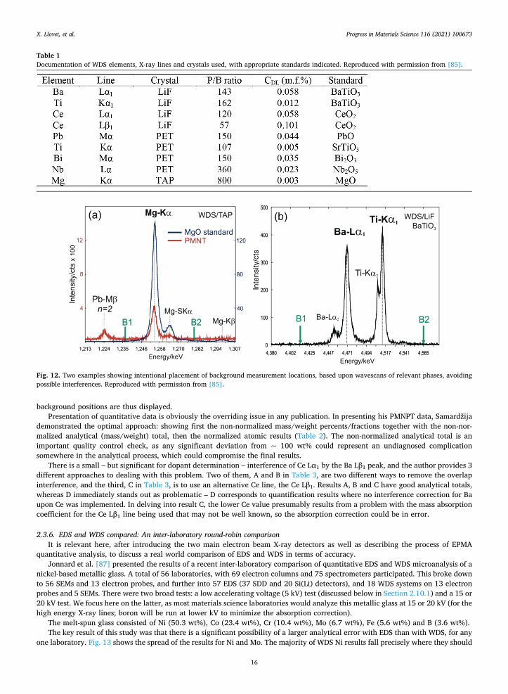
background positions are thus displayed. Presentation of quantitative data is obviously the overriding issue in any publication. In presenting his PMNPT data, Samardžija
demonstrated the optimal approach: showing first the non-normalized mass/weight percents/fractions together with the non-nor-malized analytical (mass/weight) total, then the normalized atomic results (Table 2). The non-normalized analytical total is an important quality control check, as any significant deviation from ~ 100 wt% could represent an undiagnosed complication somewhere in the analytical process, which could compromise the final results.
There is a small – but significant for dopant determination – interference of Ce Lα1 by the Ba Lβ1 peak, and the author provides 3 different approaches to dealing with this problem. Two of them, A and B in Table 3, are two different ways to remove the overlap interference, and the third, C in Table 3, is to use an alternative Ce line, the Ce Lβ1. Results A, B and C have good analytical totals, whereas D immediately stands out as problematic – D corresponds to quantification results where no interference correction for Ba upon Ce was implemented. In delving into result C, the lower Ce value presumably results from a problem with the mass absorption coefficient for the Ce Lβ1 line being used that may not be well known, so the absorption correction could be in error.
2.3.6. EDS and WDS compared: An inter-laboratory round-robin comparison It is relevant here, after introducing the two main electron beam X-ray detectors as well as describing the process of EPMA
quantitative analysis, to discuss a real world comparison of EDS and WDS in terms of accuracy. Jonnard et al. [87] presented the results of a recent inter-laboratory comparison of quantitative EDS and WDS microanalysis of a
nickel-based metallic glass. A total of 56 laboratories, with 69 electron columns and 75 spectrometers participated. This broke down to 56 SEMs and 13 electron probes, and further into 57 EDS (37 SDD and 20 Si(Li) detectors), and 18 WDS systems on 13 electron probes and 5 SEMs. There were two broad tests: a low accelerating voltage (5 kV) test (discussed below in Section 2.10.1) and a 15 or 20 kV test. We focus here on the latter, as most materials science laboratories would analyze this metallic glass at 15 or 20 kV (for the high energy X-ray lines; boron will be run at lower kV to minimize the absorption correction).
The melt-spun glass consisted of Ni (50.3 wt%), Co (23.4 wt%), Cr (10.4 wt%), Mo (6.7 wt%), Fe (5.6 wt%) and B (3.6 wt%). The key result of this study was that there is a significant possibility of a larger analytical error with EDS than with WDS, for any
one laboratory. Fig. 13 shows the spread of the results for Ni and Mo. The majority of WDS Ni results fall precisely where they should
Table 1 Documentation of WDS elements, X-ray lines and crystals used, with appropriate standards indicated. Reproduced with permission from [85].
Fig. 12. Two examples showing intentional placement of background measurement locations, based upon wavescans of relevant phases, avoiding possible interferences. Reproduced with permission from [85].
X. Llovet, et al. Progress in Materials Science 116 (2021) 100673
16
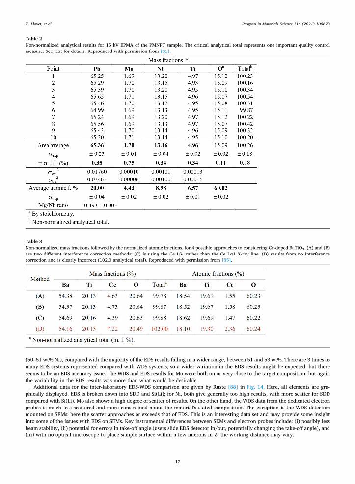
(50–51 wt% Ni), compared with the majority of the EDS results falling in a wider range, between 51 and 53 wt%. There are 3 times as many EDS systems represented compared with WDS systems, so a wider variation in the EDS results might be expected, but there seems to be an EDS accuracy issue. The WDS and EDS results for Mo were both on or very close to the target composition, but again the variability in the EDS results was more than what would be desirable.
Additional data for the inter-laboratory EDS-WDS comparison are given by Ruste [88] in Fig. 14. Here, all elements are gra-phically displayed. EDS is broken down into SDD and Si(Li); for Ni, both give generally too high results, with more scatter for SDD compared with Si(Li). Mo also shows a high degree of scatter of results. On the other hand, the WDS data from the dedicated electron probes is much less scattered and more constrained about the material's stated composition. The exception is the WDS detectors mounted on SEMs: here the scatter approaches or exceeds that of EDS. This is an interesting data set and may provide some insight into some of the issues with EDS on SEMs. Key instrumental differences between SEMs and electron probes include: (i) possibly less beam stability, (ii) potential for errors in take-off angle (users slide EDS detector in/out, potentially changing the take-off angle), and (iii) with no optical microscope to place sample surface within a few microns in Z, the working distance may vary.
Table 2 Non-normalized analytical results for 15 kV EPMA of the PMNPT sample. The critical analytical total represents one important quality control measure. See text for details. Reproduced with permission from [85].
Table 3 Non-normalized mass fractions followed by the normalized atomic fractions, for 4 possible approaches to considering Ce-doped BaTiO3. (A) and (B) are two different interference correction methods; (C) is using the Ce Lβ1 rather than the Ce Lα1 X-ray line. (D) results from no interference correction and is clearly incorrect (102.0 analytical total). Reproduced with permission from [85].
X. Llovet, et al. Progress in Materials Science 116 (2021) 100673
17
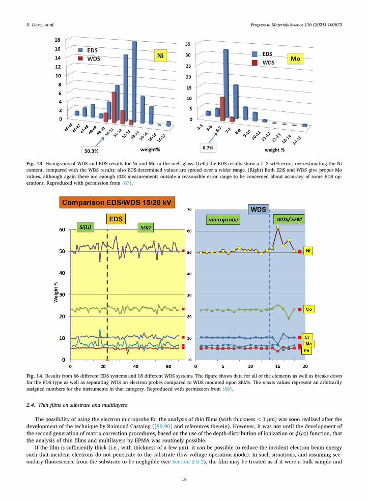
2.4. Thin films on substrate and multilayers
The possibility of using the electron microprobe for the analysis of thin films (with thickness < 1 μm) was soon realized after the development of the technique by Raimond Castaing ([89,90] and references therein). However, it was not until the development of the second generation of matrix correction procedures, based on the use of the depth-distribution of ionization or z( ) function, that the analysis of thin films and multilayers by EPMA was routinely possible.
If the film is sufficiently thick (i.e., with thickness of a few μm), it can be possible to reduce the incident electron beam energy such that incident electrons do not penetrate to the substrate (low-voltage operation mode). In such situations, and assuming sec-ondary fluorescence from the substrate to be negligible (see Section 2.5.2), the film may be treated as if it were a bulk sample and
Fig. 13. Histograms of WDS and EDS results for Ni and Mo in the melt glass. (Left) the EDS results show a 1–2 wt% error, overestimating the Ni content, compared with the WDS results; also EDS-determined values are spread over a wider range. (Right) Both EDS and WDS give proper Mo values, although again there are enough EDS measurements outside a reasonable error range to be concerned about accuracy of some EDS op-erations. Reproduced with permission from [87].
Fig. 14. Results from 66 different EDS systems and 18 different WDS systems. The figure shows data for all of the elements as well as breaks down for the EDS type as well as separating WDS on electron probes compared to WDS mounted upon SEMs. The x-axis values represent an arbitrarily assigned numbers for the instruments in that category. Reproduced with permission from [88].
X. Llovet, et al. Progress in Materials Science 116 (2021) 100673
18
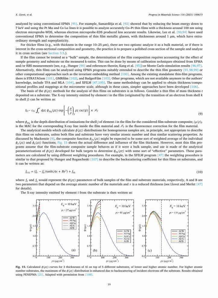
analyzed by using conventional EPMA [91]. For example, Samardžija et al. [92] showed that by reducing the beam energy down to 7 keV and using the Pt Mα and Co Lα lines it is possible to analyze accurately Co–Pt thin films with a thickness around 100 nm using electron microprobe-WDS, whereas electron microprobe-EDS produced less accurate results. Likewise, Lee et al. [93,94] have used conventional EPMA to determine the composition of thin film metallic glasses, with thicknesses around 1 μm, which have extra-ordinary strength and superplasticity.
For thicker films (e.g., with thickness in the range 10–25 μm), there are two options: analyze it as a bulk material, or if there is interest in the cross-sectional composition and geometry, the practice is to prepare a polished cross section of the sample and analyze it in cross section (see Section 3.5.).
If the film cannot be treated as a “bulk” sample, the determination of the film composition requires accounting for the effect of sample geometry and substrate on the measured k-ratios. This can be done by means of calibration techniques obtained from EPMA and/or RBS measurements (see, e.g., Hunger [90] and references therein; Kang et al. [95]) or Monte Carlo simulation results [96,97]. Alternatively, thin films can be analyzed using EPMA programs suitably extended to describe the thin film geometry [91,98,99] or other computational approaches such as the invariant embedding method [100]. Among the existing standalone thin-film programs, there is STRATAGem [101], GMRfilm [102], and BadgerFilm [103]. Other programs, which are not available anymore to the authors’ knowledge, include TFA and MLA [104], and XFILM [47,105]. The same methodology can be applied to obtain thickness/compo-sitional profiles and mappings at the micrometer scale, although in these cases, simpler approaches have been developed [106].
The basis of the z( ) methods for the analysis of thin films on substrates is as follows. Consider a thin film of mass thickness t deposited on a substrate. The X-ray intensity emitted by element i in the film (originated by the transition of an electron from shell k to shell j) can be written as:
F×I c d z z µ z~ ( ) exp csc( )i it
jF F 0 FSF
F(9)
where jFS is the depth-distribution of ionizations for shell j of element i in the film for the considered film-substrate composite, µ( / )Fis the MAC for the corresponding X-ray line inside the film material and FF is the fluorescence correction for the film material.
The analytical models which calculate z( ) distributions for homogeneous samples are, in principle, not appropriate to describe thin films on substrates, unless both film and substrate have very similar atomic number and thus similar scattering properties. As discussed by Mackenzie [9], the composite function z( )FS might be expected to be some sort of weighted average of the individual
z( )F and z( )S functions; Fig. 15 shows the actual difference and influence of the film thickness. However, most thin film pro-grams assume that the film-substrate composite sample behaves as if it were a bulk sample, and use is made of the analytical parameterizations of z( ) developed for bulk targets to determine z( )FS with some sort of “effective’’ parameters. These para-meters are calculated by using different weighting procedures. For example, in the XFILM program [47] the weighting procedure is similar to that proposed by Hunger and Rogascheski [107] to describe the backscattering coefficient for thin films on substrates, and it can be written as:
= + +f f f Ax Bx f( ) tanh( )F/S F S2
FS (10)
where fF and fS would represent the z( ) parameters of bulk samples of the film and substrate materials, respectively, A and B are two parameters that depend on the average atomic number of the materials and x is a reduced thickness (see Llovet and Merlet [47] for details).
The X-ray intensity emitted by element i from the substrate is then written as:
Fig. 15. Calculated z( ) curves for 3 thicknesses of Al on top of 5 different substrates, of lower and higher atomic number. For higher atomic number substrates, the maximum of the z( ) distribution is enhanced due to backscattering of incident electrons off the substrate. Results obtained using PENEPMA [21]. Adapted with permission from [108].
X. Llovet, et al. Progress in Materials Science 116 (2021) 100673
19
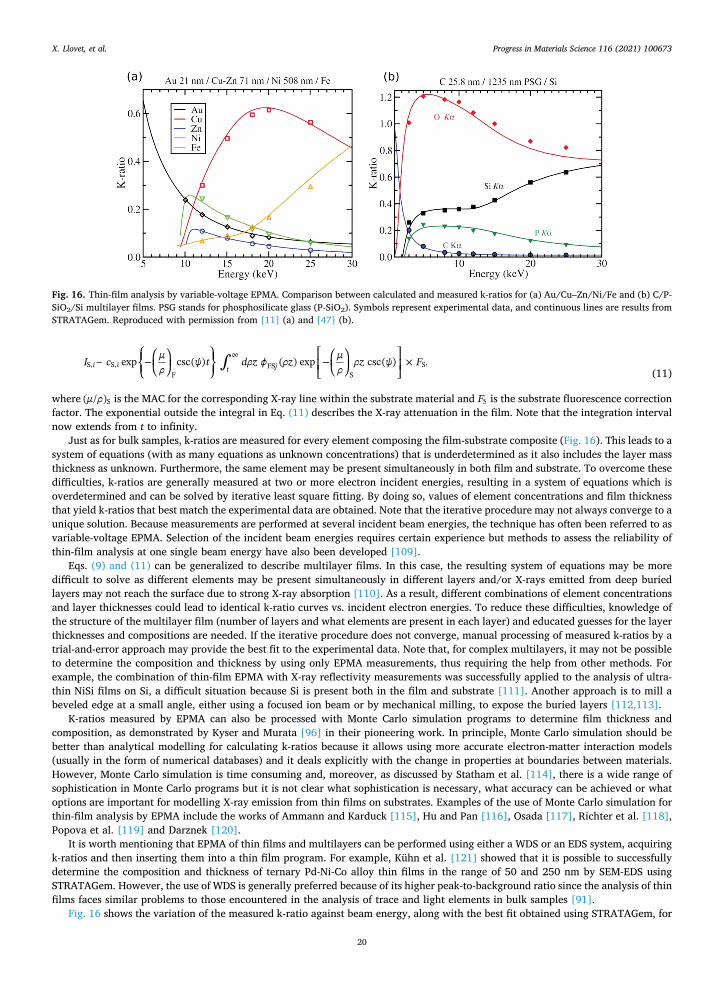
×I c µ t d z z µ z F~ exp csc( ) ( ) exp csc( ) ,i i t jS, S,F
FSS
S(11)
where µ( / )S is the MAC for the corresponding X-ray line within the substrate material and FS is the substrate fluorescence correction factor. The exponential outside the integral in Eq. (11) describes the X-ray attenuation in the film. Note that the integration interval now extends from t to infinity.
Just as for bulk samples, k-ratios are measured for every element composing the film-substrate composite (Fig. 16). This leads to a system of equations (with as many equations as unknown concentrations) that is underdetermined as it also includes the layer mass thickness as unknown. Furthermore, the same element may be present simultaneously in both film and substrate. To overcome these difficulties, k-ratios are generally measured at two or more electron incident energies, resulting in a system of equations which is overdetermined and can be solved by iterative least square fitting. By doing so, values of element concentrations and film thickness that yield k-ratios that best match the experimental data are obtained. Note that the iterative procedure may not always converge to a unique solution. Because measurements are performed at several incident beam energies, the technique has often been referred to as variable-voltage EPMA. Selection of the incident beam energies requires certain experience but methods to assess the reliability of thin-film analysis at one single beam energy have also been developed [109].
Eqs. (9) and (11) can be generalized to describe multilayer films. In this case, the resulting system of equations may be more difficult to solve as different elements may be present simultaneously in different layers and/or X-rays emitted from deep buried layers may not reach the surface due to strong X-ray absorption [110]. As a result, different combinations of element concentrations and layer thicknesses could lead to identical k-ratio curves vs. incident electron energies. To reduce these difficulties, knowledge of the structure of the multilayer film (number of layers and what elements are present in each layer) and educated guesses for the layer thicknesses and compositions are needed. If the iterative procedure does not converge, manual processing of measured k-ratios by a trial-and-error approach may provide the best fit to the experimental data. Note that, for complex multilayers, it may not be possible to determine the composition and thickness by using only EPMA measurements, thus requiring the help from other methods. For example, the combination of thin-film EPMA with X-ray reflectivity measurements was successfully applied to the analysis of ultra- thin NiSi films on Si, a difficult situation because Si is present both in the film and substrate [111]. Another approach is to mill a beveled edge at a small angle, either using a focused ion beam or by mechanical milling, to expose the buried layers [112,113].
K-ratios measured by EPMA can also be processed with Monte Carlo simulation programs to determine film thickness and composition, as demonstrated by Kyser and Murata [96] in their pioneering work. In principle, Monte Carlo simulation should be better than analytical modelling for calculating k-ratios because it allows using more accurate electron-matter interaction models (usually in the form of numerical databases) and it deals explicitly with the change in properties at boundaries between materials. However, Monte Carlo simulation is time consuming and, moreover, as discussed by Statham et al. [114], there is a wide range of sophistication in Monte Carlo programs but it is not clear what sophistication is necessary, what accuracy can be achieved or what options are important for modelling X-ray emission from thin films on substrates. Examples of the use of Monte Carlo simulation for thin-film analysis by EPMA include the works of Ammann and Karduck [115], Hu and Pan [116], Osada [117], Richter et al. [118], Popova et al. [119] and Darznek [120].
It is worth mentioning that EPMA of thin films and multilayers can be performed using either a WDS or an EDS system, acquiring k-ratios and then inserting them into a thin film program. For example, Kühn et al. [121] showed that it is possible to successfully determine the composition and thickness of ternary Pd-Ni-Co alloy thin films in the range of 50 and 250 nm by SEM-EDS using STRATAGem. However, the use of WDS is generally preferred because of its higher peak-to-background ratio since the analysis of thin films faces similar problems to those encountered in the analysis of trace and light elements in bulk samples [91].
Fig. 16 shows the variation of the measured k-ratio against beam energy, along with the best fit obtained using STRATAGem, for
Fig. 16. Thin-film analysis by variable-voltage EPMA. Comparison between calculated and measured k-ratios for (a) Au/Cu–Zn/Ni/Fe and (b) C/P- SiO2/Si multilayer films. PSG stands for phosphosilicate glass (P-SiO2). Symbols represent experimental data, and continuous lines are results from STRATAGem. Reproduced with permission from [11] (a) and [47] (b).
X. Llovet, et al. Progress in Materials Science 116 (2021) 100673
20
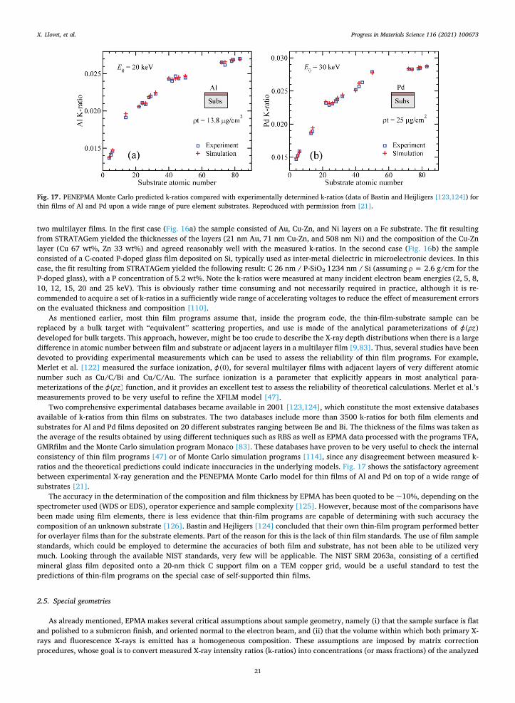
two multilayer films. In the first case (Fig. 16a) the sample consisted of Au, Cu-Zn, and Ni layers on a Fe substrate. The fit resulting from STRATAGem yielded the thicknesses of the layers (21 nm Au, 71 nm Cu-Zn, and 508 nm Ni) and the composition of the Cu-Zn layer (Cu 67 wt%, Zn 33 wt%) and agreed reasonably well with the measured k-ratios. In the second case (Fig. 16b) the sample consisted of a C-coated P-doped glass film deposited on Si, typically used as inter-metal dielectric in microelectronic devices. In this case, the fit resulting from STRATAGem yielded the following result: C 26 nm / P-SiO2 1234 nm / Si (assuming ρ = 2.6 g/cm for the P-doped glass), with a P concentration of 5.2 wt%. Note the k-ratios were measured at many incident electron beam energies (2, 5, 8, 10, 12, 15, 20 and 25 keV). This is obviously rather time consuming and not necessarily required in practice, although it is re-commended to acquire a set of k-ratios in a sufficiently wide range of accelerating voltages to reduce the effect of measurement errors on the evaluated thickness and composition [110].
As mentioned earlier, most thin film programs assume that, inside the program code, the thin-film-substrate sample can be replaced by a bulk target with “equivalent’’ scattering properties, and use is made of the analytical parameterizations of z( )developed for bulk targets. This approach, however, might be too crude to describe the X-ray depth distributions when there is a large difference in atomic number between film and substrate or adjacent layers in a multilayer film [9,83]. Thus, several studies have been devoted to providing experimental measurements which can be used to assess the reliability of thin film programs. For example, Merlet et al. [122] measured the surface ionization, (0), for several multilayer films with adjacent layers of very different atomic number such as Cu/C/Bi and Cu/C/Au. The surface ionization is a parameter that explicitly appears in most analytical para-meterizations of the z( ) function, and it provides an excellent test to assess the reliability of theoretical calculations. Merlet et al.’s measurements proved to be very useful to refine the XFILM model [47].
Two comprehensive experimental databases became available in 2001 [123,124], which constitute the most extensive databases available of k-ratios from thin films on substrates. The two databases include more than 3500 k-ratios for both film elements and substrates for Al and Pd films deposited on 20 different substrates ranging between Be and Bi. The thickness of the films was taken as the average of the results obtained by using different techniques such as RBS as well as EPMA data processed with the programs TFA, GMRfilm and the Monte Carlo simulation program Monaco [83]. These databases have proven to be very useful to check the internal consistency of thin film programs [47] or of Monte Carlo simulation programs [114], since any disagreement between measured k- ratios and the theoretical predictions could indicate inaccuracies in the underlying models. Fig. 17 shows the satisfactory agreement between experimental X-ray generation and the PENEPMA Monte Carlo model for thin films of Al and Pd on top of a wide range of substrates [21].
The accuracy in the determination of the composition and film thickness by EPMA has been quoted to be ~10%, depending on the spectrometer used (WDS or EDS), operator experience and sample complexity [125]. However, because most of the comparisons have been made using film elements, there is less evidence that thin-film programs are capable of determining with such accuracy the composition of an unknown substrate [126]. Bastin and Hejligers [124] concluded that their own thin-film program performed better for overlayer films than for the substrate elements. Part of the reason for this is the lack of thin film standards. The use of film sample standards, which could be employed to determine the accuracies of both film and substrate, has not been able to be utilized very much. Looking through the available NIST standards, very few will be applicable. The NIST SRM 2063a, consisting of a certified mineral glass film deposited onto a 20-nm thick C support film on a TEM copper grid, would be a useful standard to test the predictions of thin-film programs on the special case of self-supported thin films.
2.5. Special geometries
As already mentioned, EPMA makes several critical assumptions about sample geometry, namely (i) that the sample surface is flat and polished to a submicron finish, and oriented normal to the electron beam, and (ii) that the volume within which both primary X- rays and fluorescence X-rays is emitted has a homogeneous composition. These assumptions are imposed by matrix correction procedures, whose goal is to convert measured X-ray intensity ratios (k-ratios) into concentrations (or mass fractions) of the analyzed
Fig. 17. PENEPMA Monte Carlo predicted k-ratios compared with experimentally determined k-ratios (data of Bastin and Heijligers [123,124]) for thin films of Al and Pd upon a wide range of pure element substrates. Reproduced with permission from [21].
X. Llovet, et al. Progress in Materials Science 116 (2021) 100673
21
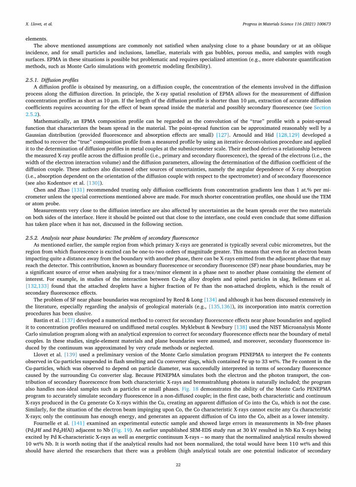
elements. The above mentioned assumptions are commonly not satisfied when analysing close to a phase boundary or at an oblique
incidence, and for small particles and inclusions, lamellae, materials with gas bubbles, porous media, and samples with rough surfaces. EPMA in these situations is possible but problematic and requires specialized attention (e.g., more elaborate quantification methods, such as Monte Carlo simulations with geometric modeling flexibility).
2.5.1. Diffusion profiles A diffusion profile is obtained by measuring, on a diffusion couple, the concentration of the elements involved in the diffusion
process along the diffusion direction. In principle, the X-ray spatial resolution of EPMA allows for the measurement of diffusion concentration profiles as short as 10 μm. If the length of the diffusion profile is shorter than 10 μm, extraction of accurate diffusion coefficients requires accounting for the effect of beam spread inside the material and possibly secondary fluorescence (see Section 2.5.2).
Mathematically, an EPMA composition profile can be regarded as the convolution of the “true” profile with a point-spread function that characterizes the beam spread in the material. The point-spread function can be approximated reasonably well by a Gaussian distribution (provided fluorescence and absorption effects are small) [127]. Arnould and Hid [128,129] developed a method to recover the “true” composition profile from a measured profile by using an iterative deconvolution procedure and applied it to the determination of diffusion profiles in metal couples at the submicrometer scale. Their method derives a relationship between the measured X-ray profile across the diffusion profile (i.e., primary and secondary fluorescence), the spread of the electrons (i.e., the width of the electron interaction volume) and the diffusion parameters, allowing the determination of the diffusion coefficient of the diffusion couple. These authors also discussed other sources of uncertainties, namely the angular dependence of X-ray absorption (i.e., absorption dependent on the orientation of the diffusion couple with respect to the spectrometer) and of secondary fluorescence (see also Kodentsov et al. [130]).
Chen and Zhao [131] recommended trusting only diffusion coefficients from concentration gradients less than 1 at.% per mi-crometer unless the special corrections mentioned above are made. For much shorter concentration profiles, one should use the TEM or atom probe.
Measurements very close to the diffusion interface are also affected by uncertainties as the beam spreads over the two materials on both sides of the interface. Here it should be pointed out that close to the interface, one could even conclude that some diffusion has taken place when it has not, discussed in the following section.
2.5.2. Analysis near phase boundaries: The problem of secondary fluorescence As mentioned earlier, the sample region from which primary X-rays are generated is typically several cubic micrometres, but the
region from which fluorescence is excited can be one-to-two orders of magnitude greater. This means that even for an electron beam impacting quite a distance away from the boundary with another phase, there can be X-rays emitted from the adjacent phase that may reach the detector. This contribution, known as boundary fluorescence or secondary fluorescence (SF) near phase boundaries, may be a significant source of error when analysing for a trace/minor element in a phase next to another phase containing the element of interest. For example, in studies of the interaction between Cu-Ag alloy droplets and spinel particles in slag, Bellemans et al. [132,133] found that the attached droplets have a higher fraction of Fe than the non-attached droplets, which is the result of secondary fluorescence effects.
The problem of SF near phase boundaries was recognized by Reed & Long [134] and although it has been discussed extensively in the literature, especially regarding the analysis of geological materials (e.g., [135,136]), its incorporation into matrix correction procedures has been elusive.
Bastin et al. [137] developed a numerical method to correct for secondary fluorescence effects near phase boundaries and applied it to concentration profiles measured on undiffused metal couples. Myklebust & Newbury [138] used the NIST Microanalysis Monte Carlo simulation program along with an analytical expression to correct for secondary fluorescence effects near the boundary of metal couples. In these studies, single-element materials and plane boundaries were assumed, and moreover, secondary fluorescence in-duced by the continuum was approximated by very crude methods or neglected.
Llovet et al. [139] used a preliminary version of the Monte Carlo simulation program PENEPMA to interpret the Fe contents observed in Cu-particles suspended in flash smelting and Cu converter slags, which contained Fe up to 33 wt%. The Fe content in the Cu-particles, which was observed to depend on particle diameter, was successfully interpreted in terms of secondary fluorescence caused by the surrounding Cu converter slag. Because PENEPMA simulates both the electron and the photon transport, the con-tribution of secondary fluorescence from both characteristic X-rays and bremsstrahlung photons is naturally included; the program also handles non-ideal samples such as particles or small phases. Fig. 18 demonstrates the ability of the Monte Carlo PENEPMA program to accurately simulate secondary fluorescence in a non-diffused couple; in the first case, both characteristic and continuum X-rays produced in the Cu generate Co X-rays within the Cu, creating an apparent diffusion of Co into the Cu, which is not the case. Similarly, for the situation of the electron beam impinging upon Co, the Co characteristic X-rays cannot excite any Cu characteristic X-rays; only the continuum has enough energy, and generates an apparent diffusion of Cu into the Co, albeit as a lower intensity.
Fournelle et al. [141] examined an experimental eutectic sample and showed large errors in measurements in Nb-free phases (Pd3Hf and Pd2HfAl) adjacent to Nb (Fig. 19). An earlier unpublished SEM-EDS study run at 30 kV resulted in Nb Kα X-rays being excited by Pd K-characteristic X-rays as well as energetic continuum X-rays – so many that the normalized analytical results showed 10 wt% Nb. It is worth noting that if the analytical results had not been normalized, the total would have been 110 wt% and this should have alerted the researchers that there was a problem (high analytical totals are one potential indicator of secondary
X. Llovet, et al. Progress in Materials Science 116 (2021) 100673
22
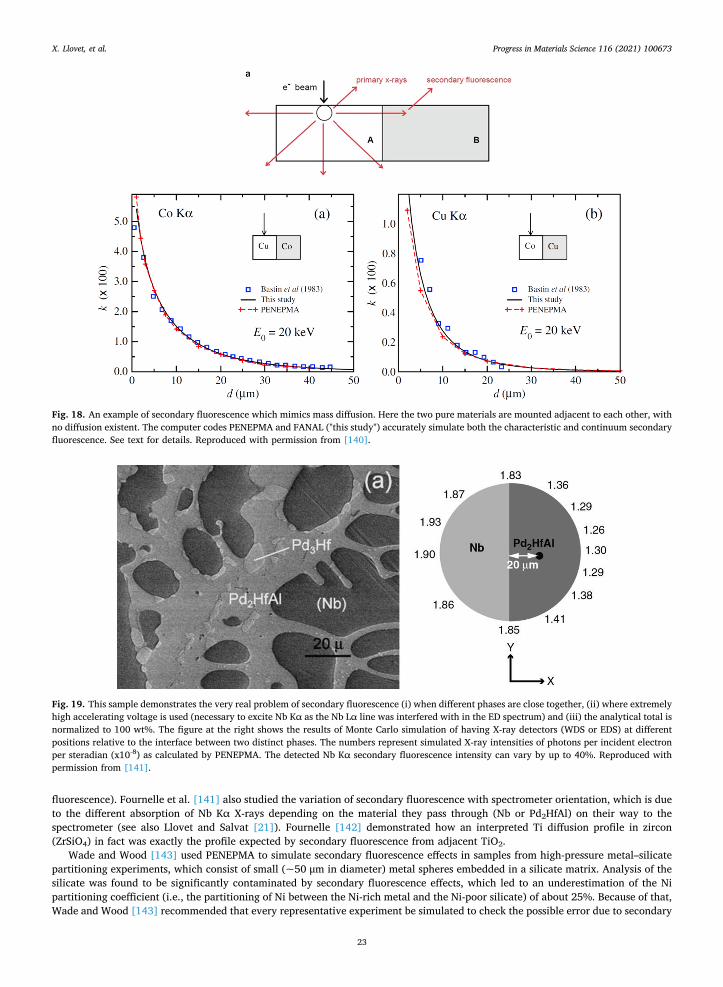
fluorescence). Fournelle et al. [141] also studied the variation of secondary fluorescence with spectrometer orientation, which is due to the different absorption of Nb Kα X-rays depending on the material they pass through (Nb or Pd2HfAl) on their way to the spectrometer (see also Llovet and Salvat [21]). Fournelle [142] demonstrated how an interpreted Ti diffusion profile in zircon (ZrSiO4) in fact was exactly the profile expected by secondary fluorescence from adjacent TiO2.
Wade and Wood [143] used PENEPMA to simulate secondary fluorescence effects in samples from high-pressure metal–silicate partitioning experiments, which consist of small (~50 μm in diameter) metal spheres embedded in a silicate matrix. Analysis of the silicate was found to be significantly contaminated by secondary fluorescence effects, which led to an underestimation of the Ni partitioning coefficient (i.e., the partitioning of Ni between the Ni-rich metal and the Ni-poor silicate) of about 25%. Because of that, Wade and Wood [143] recommended that every representative experiment be simulated to check the possible error due to secondary
Fig. 18. An example of secondary fluorescence which mimics mass diffusion. Here the two pure materials are mounted adjacent to each other, with no diffusion existent. The computer codes PENEPMA and FANAL ("this study") accurately simulate both the characteristic and continuum secondary fluorescence. See text for details. Reproduced with permission from [140].
Fig. 19. This sample demonstrates the very real problem of secondary fluorescence (i) when different phases are close together, (ii) where extremely high accelerating voltage is used (necessary to excite Nb Kα as the Nb Lα line was interfered with in the ED spectrum) and (iii) the analytical total is normalized to 100 wt%. The figure at the right shows the results of Monte Carlo simulation of having X-ray detectors (WDS or EDS) at different positions relative to the interface between two distinct phases. The numbers represent simulated X-ray intensities of photons per incident electron per steradian (x10-8) as calculated by PENEPMA. The detected Nb Kα secondary fluorescence intensity can vary by up to 40%. Reproduced with permission from [141].
X. Llovet, et al. Progress in Materials Science 116 (2021) 100673
23
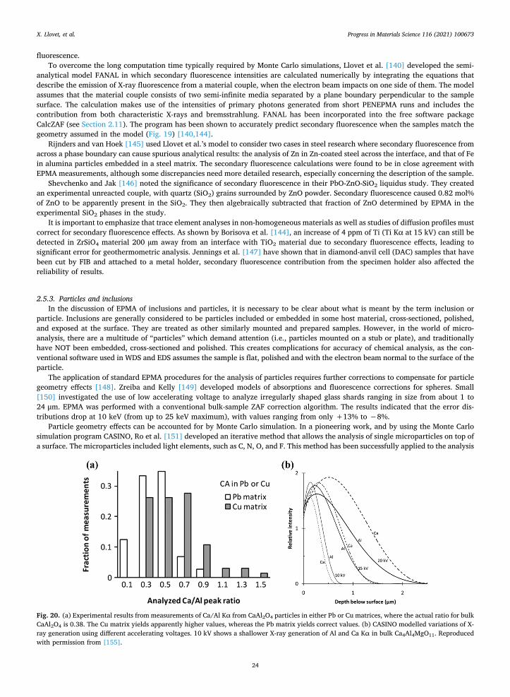
fluorescence. To overcome the long computation time typically required by Monte Carlo simulations, Llovet et al. [140] developed the semi-
analytical model FANAL in which secondary fluorescence intensities are calculated numerically by integrating the equations that describe the emission of X-ray fluorescence from a material couple, when the electron beam impacts on one side of them. The model assumes that the material couple consists of two semi-infinite media separated by a plane boundary perpendicular to the sample surface. The calculation makes use of the intensities of primary photons generated from short PENEPMA runs and includes the contribution from both characteristic X-rays and bremsstrahlung. FANAL has been incorporated into the free software package CalcZAF (see Section 2.11). The program has been shown to accurately predict secondary fluorescence when the samples match the geometry assumed in the model (Fig. 19) [140,144].
Rijnders and van Hoek [145] used Llovet et al.’s model to consider two cases in steel research where secondary fluorescence from across a phase boundary can cause spurious analytical results: the analysis of Zn in Zn-coated steel across the interface, and that of Fe in alumina particles embedded in a steel matrix. The secondary fluorescence calculations were found to be in close agreement with EPMA measurements, although some discrepancies need more detailed research, especially concerning the description of the sample.
Shevchenko and Jak [146] noted the significance of secondary fluorescence in their PbO-ZnO-SiO2 liquidus study. They created an experimental unreacted couple, with quartz (SiO2) grains surrounded by ZnO powder. Secondary fluorescence caused 0.82 mol% of ZnO to be apparently present in the SiO2. They then algebraically subtracted that fraction of ZnO determined by EPMA in the experimental SiO2 phases in the study.
It is important to emphasize that trace element analyses in non-homogeneous materials as well as studies of diffusion profiles must correct for secondary fluorescence effects. As shown by Borisova et al. [144], an increase of 4 ppm of Ti (Ti Kα at 15 kV) can still be detected in ZrSiO4 material 200 µm away from an interface with TiO2 material due to secondary fluorescence effects, leading to significant error for geothermometric analysis. Jennings et al. [147] have shown that in diamond-anvil cell (DAC) samples that have been cut by FIB and attached to a metal holder, secondary fluorescence contribution from the specimen holder also affected the reliability of results.
2.5.3. Particles and inclusions In the discussion of EPMA of inclusions and particles, it is necessary to be clear about what is meant by the term inclusion or
particle. Inclusions are generally considered to be particles included or embedded in some host material, cross-sectioned, polished, and exposed at the surface. They are treated as other similarly mounted and prepared samples. However, in the world of micro-analysis, there are a multitude of “particles” which demand attention (i.e., particles mounted on a stub or plate), and traditionally have NOT been embedded, cross-sectioned and polished. This creates complications for accuracy of chemical analysis, as the con-ventional software used in WDS and EDS assumes the sample is flat, polished and with the electron beam normal to the surface of the particle.
The application of standard EPMA procedures for the analysis of particles requires further corrections to compensate for particle geometry effects [148]. Zreiba and Kelly [149] developed models of absorptions and fluorescence corrections for spheres. Small [150] investigated the use of low accelerating voltage to analyze irregularly shaped glass shards ranging in size from about 1 to 24 μm. EPMA was performed with a conventional bulk-sample ZAF correction algorithm. The results indicated that the error dis-tributions drop at 10 keV (from up to 25 keV maximum), with values ranging from only +13% to −8%.
Particle geometry effects can be accounted for by Monte Carlo simulation. In a pioneering work, and by using the Monte Carlo simulation program CASINO, Ro et al. [151] developed an iterative method that allows the analysis of single microparticles on top of a surface. The microparticles included light elements, such as C, N, O, and F. This method has been successfully applied to the analysis
Fig. 20. (a) Experimental results from measurements of Ca/Al Kα from CaAl2O4 particles in either Pb or Cu matrices, where the actual ratio for bulk CaAl2O4 is 0.38. The Cu matrix yields apparently higher values, whereas the Pb matrix yields correct values. (b) CASINO modelled variations of X- ray generation using different accelerating voltages. 10 kV shows a shallower X-ray generation of Al and Ca Kα in bulk Ca4Al4MgO11. Reproduced with permission from [155].
X. Llovet, et al. Progress in Materials Science 116 (2021) 100673
24

of atmospheric particles [152] and mineral particles [153]. Ritchie [154] demonstrated the ability of the NIST DTSA-II program’s Monte Carlo to simulate particle-upon-substrate electron and X-ray behavior, and that it demonstrated that electrons that exited the particle, can re-enter and generate a significant number of X-rays.
Pistorius and Verma [155], evaluated the treatment of alumina and spinel inclusions in steel by calcium modification. The Ca/Al ratio of inclusions affects the castability of steel. After treatment, the inclusions are typically smaller than two microns in apparent diameter and it is difficult to accurately determine by EPMA the Ca/Al and Mg/Al ratios. They used Monte Carlo simulations (DTSA- II; PENEPMA) together with experiments to show that the softer Al X-rays suffered more absorption by the steel matrix, over-estimating the Ca/Al ratio (Fig. 20). They emphasize that this problem stems from the fact that the traditional bulk matrix correction is not applicable for EPMA of an inclusion in a different matrix. They then demonstrated that dropping the beam energy from 15 to 10 kV yielded improved results.
2.5.4. Porous materials, rough surfaces and others EPMA of mesoporous alumina, commonly used as a catalyst host, results in unrealistically low analytical totals, as documented by
Lakis et al. [156,157]. In this study, porous-alumina-supported platinum catalysts were examined at a range of accelerating voltages (10, 15, 25 kV) and fully dense α-alumina was used as the aluminum and oxygen standard. Al Kα intensity in the porous material was only 75% of that in the dense reference material, and O Kα was only 60% of the standard—regardless of accelerating voltage.
Sorbier et al. [158] used Monte Carlo modelling to demonstrate that the geometric effect of porosity could not explain the lower X-ray intensity, relative to a dense bulk standard of the same chemical composition. Further investigation [159] led them to conclude that previously suggested charge trapping was not the explanation. Rather, the problems in the lower-than-expected X-ray counts for Al and O Kα were due to (i) the porous alumina having a different composition from stoichiometric Al2O3 (with possibly structural and absorbed water) and (ii) penetration of epoxy components into the pores of the mesoporous alumina. This was documented upon including carbon as a measured element. They concluded with advice for EPMA of such porous material: be cautious of assumptions of exact composition relative to nominally similar bulk materials and be aware that a slight (e.g., carbon) contamination layer on thin porous surfaces has a significantly higher contribution compared to the same thickness upon a bulk material.
Gopon [160] examined exsolution lamellae in lunar pyroxenes. Conventional 15–20 kV EPMA had been limited to lamellae widths of 6–8 µm [161]. Using 7 kV with a field emission electron probe and corrections for secondary fluorescence by PENEPMA (using the interface pyPENELOPE developed by Pinard et al. [84]), Gopon was able to determine lamellae compositions of ~ 1 µm and below. For example, for a Ca-poor pyroxene lamella 1.5-µm wide inside a Ca-rich pyroxene host, the Monte Carlo simulation results showed that secondary fluorescence added 7 relative% Ca; for a smaller, 600 nm lamellae, 9 relative % of the Ca was from secondary fluorescence effects. With these values, the EPMA results were able to be corrected and the secondary fluorescence X-ray intensities removed from the results.
In EPMA of nuclear fuel, one important phase is not a solid, but a gas trapped in the solid as bubbles. A method to analyze by EPMA these gas bubbles distributed in the solid was developed by Verwerft [162] and was applied to the analysis of xenon fission gas trapped in irradiated UO2 nuclear fuel. More accurate analysis of gas retained in nuclear fuel may lead to a better insight in the gas release mechanisms. Verwerft’s method was based on the geometric modelling of gas bubble dispersion and the assessment of its influence on the emitted X-ray intensity and made use of experimental results obtained at different accelerating voltages.
Additionally, in experimental compounds produced in Ar-rich environments, it is not uncommon for some Ar to become trapped in the sputtered solid products. Low analytical totals result; use of virtual standards (Section 2.3.2) can be used to quantify the argon present [163].
As mentioned previously, EPMA assumes flat specimens, but in some cases, specimens must be analyzed without any surface preparation either because they cannot be destroyed or because the information of interest is in the surface itself. The analysis of rough targets is challenging because of the dependence of the measured X-ray intensities on the topography of the sample surface [164]. For example, when analyzing technical surfaces with a roughness resulting from the rolling or coating process, EPMA results are biased. Busch and Forster [165] developed a method to correct for surface roughness and applied it to electrolytically galvanized and hot-dip galvanized steel sheet of varying roughness. More recently, Sánchez-Gonzalo et al. [166] developed a tracking algorithm in which the microscopic topography of the surface is described by an altitude map. The algorithm has been coupled to the PEN-ELOPE/PENEPMA program and allows simulations of X-ray emission from a sample with rough surfaces. It is worth pointing out that there are electron probes with inclined spectrometers, generally used in industry, for qualitative X-ray mapping of rough surfaces.
Pouchou et al. [167] and Bastin et al. [167,169] developed modifications to their respective XPP and PROZA96 z( ) matrix corrections, to be able to acquire quantitative EDS and WDS EPMA when the specimen is tilted. This technique is very useful for the simultaneous EDS-EBSD analysis, as the flat polished specimen is tilted typically at 70° to the incident electron beam. With the very limited experimental data available, their extension gave promising results [170]. These modifications have also been developed for the XFILM z( ) matrix correction [171] and for the Packwood model [12] but they are only scarcely used (e.g., Burdet et al. [172]) as the normal geometry is usually preferred.
2.6. Light elements
Light elements in EPMA are today considered the elements Li through F, with the addition of Li to the list occurring in the past half-decade. Bastin and Heijligers pioneered much of the advances in EPMA of B, C, N and O with their research, with a series of reports and publications from the late 1980s through the 1990s, which were collected in a book in 2011 [173]. WDS has been the optimal technique for light element analysis, given its better sensitivity and spectral resolution compared with EDS. However, EPMA
X. Llovet, et al. Progress in Materials Science 116 (2021) 100673
25

of light elements requires extra special attention because of the following issues:
(i) The fluorescence yield of light elements is much lower than that of heavier elements, which means that fewer X-rays are produced in favor of Auger electrons (after the atoms have been ionized in an inner-shell by incident electrons). In the early decades of EPMA, diffraction of long wavelength X-rays of the light elements required the use of wide-spaced 2d pseudocrystals such as Pb-stearate Langmuir Blodgett structures (“soap films”). Pb-stearate pseudocrystals suffered low count rates, although relatively good spectral resolution. In the early 1980s, with the commercial availability of vacuum deposited (sputtered or evaporated) alternately layered Wi/Si, Ni/C, V/C and Mo/B4C multilayered diffractors, more electron microprobe labs began to consider investigating the light elements. These diffractors, going by various names, i.e., Layered Diffracting Elements LDEs, Layered Synthetic Microstructures LSMs, as well as pseudocrystals PCs, offered much higher count rate, and 2d’s large enough (150–200 Å) to diffract Be Kα (see e.g., Hombourger et al. [174]), and in 2018, to diffract Li (see Section 2.12.2).
(ii) Because usually the count rates of the light elements are low in the unknown compound, high currents are used for the measurement of the unknown. However, if the same high current is used for the pure element standard, the pulse in the PHA window can be dramatically reduced several volts (“pulse height depression”, i.e., shifted to the left) and standard reference counts will be clipped off (see Appendix C.2.1). Tight differential PHA settings can be particularly troublesome. The general rule is that the count rate on the standard should match the count rate on the unknown, in setting up the PHA and in counting on the standard.
(iii) The spectral distance between X-ray lines of different elements decreases with their X-ray energy. This is especially true for X- ray lines with an energy below 1 keV where the K X-ray peak of light elements overlaps with the L, M or N X-ray peaks of heavier elements, even with the high spectral resolution of WDS. As a result, spectral interferences are an important source of error for light elements. These can be first order (e.g., Mo Mξ on B Kα) or higher order, both on peak (e.g., 3rd order P Kα on F Kα) or on the sides where backgrounds might be positioned (e.g., Ba Mα and Mξ adjacent to F Kα). The layered synthetic diffractors work both for and against the analyst: the count rates are much higher but the peaks are much broader than with the
Fig. 21. Using 5 keV beam energy, there is less absorption, and thus less correction (where error is introduced). Boron measured with a 200 Å LDE on a CAMECA electron probe sits at the low end of the spectrometer, where the background is higher, but there is also specular reflectance of silicon in this example of silicate glass. The accuracy of the measurements using this careful approach is shown. Reproduced with permission from [175].
X. Llovet, et al. Progress in Materials Science 116 (2021) 100673
26
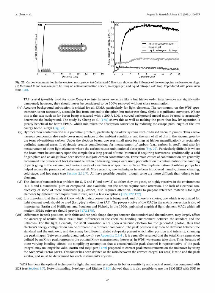
TAP crystal (possibly used for some X-rays) so interferences are more likely but higher order interferences are significantly dampened; however, they should never be considered to be 100% removed without close examination.
(iv) Accurate background subtraction is critical for all EPMA, particularly for light elements. The continuum, on the WDS spec-trometer, is not necessarily a straight line from one end to the other, but rather can show slight to significant curvature. Where this is the case such as for boron being measured with a 200 Å LDE, a curved background model must be used to accurately determine the background. The study by Cheng et al. [175] shows this as well as making the point that low kV operation is greatly beneficial for boron EPMA, which minimizes the absorption correction by reducing the escape path length of the low energy boron X-rays (Fig. 21).
(v) Hydrocarbon contamination is a potential problem, particularly on older systems with oil-based vacuum pumps. Thin carbo-naceous compounds also easily cover most surfaces under ambient conditions, and the sum of all of this in the vacuum goes by the term adventitious carbon. Under the electron beam, one sees small spots (or rings at higher magnification) or rectangles outlining scanned areas. It obviously creates complications for measurement of carbon (e.g., carbon in steel), and also for measurement of other light elements where the carbon causes unintentional absorption (Fig. 22). Particularly difficult is where the beam must be stationary upon the sample for a long period of time (minutes) if acquiring wavescans. Traditionally, a cold finger/plate and an air jet have been used to mitigate carbon contamination. Three main causes of contamination are generally recognized: the presence of backstreamed oil when oil-bearing pumps were used, poor attention to contamination-free handling of parts going in the vacuum, and various levels of cleanliness of specimen surfaces. The implementation of oil-free pumps has helped reduce the presence of backstreamed oil. More recently, new techniques have been introduced namely, plasma cleaning, cold stage, and hot stage (see Section 2.12.7). All have possible benefits, though some are more difficult than others to im-plement.
(vi) The choice of standards is a problem for O, N and F (and now Li) as either they are gases, or highly reactive in the environment (Li). B and C standards (pure or compound) are available, but the others require some attention. The lack of electrical con-ductivity of some of these standards (e.g., oxides) also requires attention. Efforts to prepare reference materials for light elements by different techniques remain rare, with a few exceptions [172,177,177].
(vii) It is important that the analyst know which matrix correction is being used, and if there is a choice, one which is optimized for light element work should be used (i.e., z( ) rather than ZAF). The proper choice of the MAC in the matrix correction is also of importance. Bastin and Heijligers, and Pouchou and Pichoir, in the 1990s, published empirical light element MACs which all modern EPMA software should provide [172,178].
(viii) Differences in peak positions, with shifts and/or peak shape changes between the standard and the unknown, may largely affect the accuracy of results. These result from differences in the chemical bonding environment between the standard and the unknown. For the light elements, the shell ionization relies upon a valence electron for the generated photon, thus that electron’s energy configuration can be different in a different compound. The peak position may then be different between the standard and the unknown, and there may be different related sub-peaks present which alter position and intensity, changing the peak shapes (between standard and unknown), see Appendix C.2.4 . It is generally assumed that the total X-ray generation defined by an X-ray peak represents the optimal X-ray measurement; however, in WDS, wavescans take time. Thus, because of these varying bonding effects, the simplifying assumption that a central/middle peak channel is representative of the peak integral may no longer be valid. Bastin and Heijligers [179] proposed to correct peak measurements on the unknown by using the Area/Peak Factor (APF). This factor has been defined as the ratio between the correct integral (or area) k-ratio and the peak k-ratio, and must be determined for each instrument’s crystals.
WDS has been the optimal technique for light element analysis, given its better sensitivity and spectral resolution compared with EDS (see Section 3.7). Notwithstanding, Newbury and Ritchie [180] showed that it is also possible to use the SEM-EDS with SDD to
Fig. 22. Carbon contamination in the electron microprobe. (a) Calculated C line scan showing the influence of the overlapping carbonaceous rings. (b) Measured C line scans on pure Fe using no anticontamination device, an oxygen jet, and liquid nitrogen cold trap. Reproduced with permission from [28].
X. Llovet, et al. Progress in Materials Science 116 (2021) 100673
27
analyze fluorides, oxides, nitrides, carbides, and borides with an accuracy of ± 5% relative. Note that quantification was performed using the NIST DTSA-II EDS software, with the local standards-based “k-ratio” method along with the PAP matrix correction method. The analytical strategy involved collection of high-count spectra measured with an input count rate that restricted the deadtime down to ~10% to minimize coincidence (sum peaks) effects. To maximize the production of X-rays, a 5 keV electron beam was used to analyze elements with excitation energies below 3 keV and an electron beam of 10 keV was employed to excite the K and L X-ray lines of intermediate and high Z elements with critical excitation energies above 3 keV.
Over the past decades, EPMA has moved forward with a combination of technical developments, allowing advances in mea-surements of the light elements. Three instrumental developments are significant here: (i) the WD parallel beam spectrometer, with a flat crystal (or multilayer), collimating a beam to a detector. This can be mounted on either an electron probe or an SEM. (ii) The newest development for light element detection—down to Li—is a spectrometer with a grating and a sensitive CCD camera named SXES (soft X-ray emission spectrometer). This permits good spectral resolution, significant P/B ratio, together with a simultaneous collection of a range of energies, essentially EDS with WDS resolution. (iii) The third development consists of windowless ED spectrometers with better energy resolution and lower noise allowing the detection of X-ray lines below 200 eV, including Li K. These instrumental developments will be discussed in detail in Sections 2.12.3-2.12.5.
2.7. Actinide elements
EPMA instruments dedicated to the analysis of actinide elements are generally installed in lead shielded rooms (hot cells) and customized for remote control. In these instruments, the radiation background coming from the intense β and γ radiation emitted from the samples is reduced by shielding the microprobe stage with plates or a massive piece of denal (95 wt% of W and 5 wt% of Cu or Fe) and by shielding the inside of the WDS with the same material at the level of the entrance window and at the level of the gas counter [181]. Lead and tungsten can also be used to shield the microprobe instead of the denal material [181,183]. To further reduce the background level, spectrometers with a larger Rowland circle can be used, and strong magnets can be installed before the spectrometer window to deflect β emissions and backscattered electrons. Many CAMECA electron microprobe models have been successfully shielded for the analysis of irradiated materials, following the pioneering work by Kleykamp and Walker in the late 1970s [68,184]. Restani and Wälchli [185] have also described the modifications required to modify a conventional JEOL electron microprobe for the examination of nuclear materials.
Another difficulty of the analysis of actinide elements is that some of the transuranic isotopes have a relatively short half-file (< 1000 years) and will decay over time. This is the case, for example, of the U-Pu-Am standards where the isotope 241Pu can decay into 241Am. The composition of the standard will then change over time. By knowing the composition of the standard (mass fraction and isotope fraction of each constituents) at a given time, it is possible to calculate the evolution of the constituents and thus to predict the standard composition at any time, assuming homogeneity. The uncertainty in the estimation of the composition of the standard will affect that of the evaluated concentrations, especially if one of the decay-produced elements is in small proportion as compared to the element that produces it.
In the case of EDS analysis, the additional X-rays accompanying the different radioactive decay processes are also a source of uncertainty as they can be detected owing to the large solid angle of EDS detectors. In the case of WDS, the focusing geometry of the spectrometer minimizes the radioactive contribution, which generally comes from a region much larger than the electron-excited region. These extra X-rays can partially be removed by subtracting a spectrum recorded with the beam turned off.
Because of the high ionization energies required to remove the K-shell electrons of actinide elements, the K-lines cannot be excited by conventional EPMA instruments. L-lines can be excited, as their ionization energies range between ~16 keV (L3 subshell of actinium) and ~20 keV (L3 subshell of einsteinium), but not efficiently as the maximum accelerating voltage available in the con-ventional EPMA instruments is 30 kV (the X-ray production is maximized when the electron beam energy is ~2–3 times the critical ionization energy). Therefore, the M lines are generally used for the analysis of actinides, but even the energies of the M-lines of actinides are not well documented. Also, the MACs of the elements Np, Pu, Am and Cm are poorly known because of difficulties in determining them experimentally [182]. Note that most MAC tabulations stop at Z = 92. If the method of virtual standards is used (see Section 2.3.2), the fluorescence yield is also required and this parameter is also poorly documented for the M sub-shells of actinide elements.
2.8. Trace elements
Trace elements have an influence on the microstructure and properties of many materials. The content of these elements in a bulk material can be determined by using chemical analysis techniques such as XRF, GDS, ICP-MS, etc. but for the determination of their distribution in the different material phases, a microbeam analysis technique such as EPMA is required. For example, Qian et al. [186] used an electron microprobe to study the addition of trace amounts of Mn into intermetallic phases in low iron Al-Si piston alloys. When most of the Mn exists in the dendritic Al9FeNi phase, the elevated temperature strengthening effect is good. Further increase of Mn addition can lead to the formation of a plate-like Mn-bearing phase, whose strengthening effect is poor. Thus, to obtain the highest elevated temperature tensile strength, Mn should be properly added according to the content of Fe in the piston alloy. Sadeghi and Pekguleryuz [187] used an electron microprobe to analyze the effect of low concentrations of Sr (0.01, 0.02 and 0.05 wt %) on the microstructure, mechanical properties and texture of an AZ31 magnesium alloy. The addition of low concentrations of Sr produces grain and precipitate refinement, which largely affects the hot deformation behavior of this alloy, reducing the strength of the basal texture in hot compression and extrusion. Another example is the concentration of Sc in Al-Cu-Li alloys, which has been
X. Llovet, et al. Progress in Materials Science 116 (2021) 100673
28
studied by Jia et al. [188] by EPMA. Adding Sc into these alloys leads to the formation of a W phase, which exerts a negative influence on the precipitation of an Al3Sc phase and of Cu-containing phases in the Al–Cu–Li alloy.
One important parameter for trace analysis is the limit of detection. This is the question of how small a variation in the back-ground (i.e., a small characteristic X-ray peak) can be distinguished from the normal statistical variability of the background. As mentioned before, evaluating the counting statistics involves taking the square root of the counts as a measure of one sigma variability. For a 99% level of confidence that a small peak is significantly different from the background, one commonly accepted rule is that it must be greater than 3 times the statistical deviation of the background (ISO 17470 [189]). Consider this example: counting for 10 s, the background counts are 100, then 3 σ would be 30, and an on-peak measurement would need to be greater than 130 counts to be considered significant (i.e., the limit of detection is 130 counts). The improvement of the detection limit by a factor of 2 (drop the detection limit to 115 counts), requires 4 times the number of counts – thus one could increase the counting time by a factor of 4, to 40 s. To state this in terms of elemental concentration, one inserts peak and background counts from a reference standard, but the critical counts are the background counts from the unknown sample. Several equations have been derived to calculate the limit of detection in terms of element concentration. As an example, a simple formula to obtain the detection limit (DL) is based upon Ziebold [52], with slight modification:
=×
× ××DL wt
I tI t I t
ZAF C wt( %)3
( %)b b
pstd
pstd
bstd
bstd
std
(12)
where Ib and tb, are the X-ray intensity (in count per second) and measuring time (in seconds) for the background on the sample, respectively. Ipstd and Ibstd are the peak intensity and background intensity on the standard, respectively. tpstd and tbstd are the measuring time for the peak and background on the standard, respectively. ZAF is the matrix correction factor (see Eq. (5)), and C wt( %)std is the mass concentration of the element of interest on the standard. Note that the leading coefficient, here “3″, is sometimes varied, dependent upon the exact level of confidence being desired (99.5%, 99.7%, 99.9%) as being distinct from the null hypothesis (i.e., the element of interest is not present).
Another formula based on a more refined statistical approach is given by Merlet and Bodinier [190] (with slight modification):
=DL wtI
tZAF C wt
I I( %)
3 2 ( %)b
b
std
pstd
bstd
(13)
where the terms are the same as previously defined. Here, a factor of 2 comes from the assumption that, as the concentration approaches the detection limit, the total intensity Ip approaches the background intensity Ib. This last equation, similar to the detection limit given in the ISO 17470 [189], is utilized by some EPMA quantification software.
It is useful to note that one user-definable variable that governs X-ray intensity is the overvoltage, whereby the probability of X- ray emission increases as the accelerating voltage increases. Newbury [191] showed that the peak-to-background ratio P/B (of a reference material using a particular crystal of WDS or specific EDS detector) can be approximated by:
PB Z
U1 ( 1)n(14)
where U is the overvoltage ratio and n is an exponent typically in the range 0.3 to 0.7. It follows from Eq. (14) that P/B increases with increasing accelerating voltage, therefore, by operating the EPMA instrument at a high overvoltage, the detection limit that can be obtained for a given beam current and counting time will be lower (although there are cases where strongly absorbed elements in certain matrices, may not see benefit with this, as X-ray generation is driven deeper in the sample). Note that the latter two factors (beam current, counting time) govern the precision of analyses, and it is the reduction of the analytical variability of the background (i.e., 3 sigma) which provides the ability to confidently measure smaller and smaller concentrations. It also follows from Eq. (14) that WDS will yield lower detection limits than EDS, owing to its better spectral resolution (thus lower background counts per eV channel) and therefore higher peak-to-background ratio.
The use of EPMA for the analysis of trace elements has increased over the years mainly because of the improved stability of electron columns operated at high beam currents and of the development of new crystal analyzers (i.e., LDEs) with larger areas. These developments have made it possible to decrease the detection limits of EPMA down to a few parts per million by simply using high accelerating voltages, high beam currents and long acquisition times. However, the accuracy of EPMA results may worsen at low concentration levels as sources of systematic errors are magnified. Operating the EPMA instrument at a high voltage and a high current also deteriorates the spatial resolution and may increase the matrix correction factors, especially that of absorption. The most important sources of systematic errors are background subtraction errors, interferences (overlaps) from other elements, sample change during analysis (beam damage), secondary fluorescence from adjacent phases, carbon contamination, and instrumental errors such as holes in the background (see Appendix C.2.5).
Several studies have examined the issues that affect the accuracy of trace analysis by EPMA (see e.g., [191-196]). Batanova et al. [196,198] concentrated on the practical aspects of trace element analysis in geological materials, namely the mineral olivine, showing that it is possible to achieve detection limits as low as 4–10 ppm, with similar precision (2σ) for individual analyses .
The conventional method of background subtraction by linear interpolation of two measurements on each side of the peak may lead to unacceptable errors for trace elements, where there is a curvature of the background. Setting the background positions much closer to the peak position is useful but may not reduce these errors. An improved method consists of a least-square fitting of several background measurements performed on different energy channels. Detailed wavelength scans around the peak of interest are
X. Llovet, et al. Progress in Materials Science 116 (2021) 100673
29
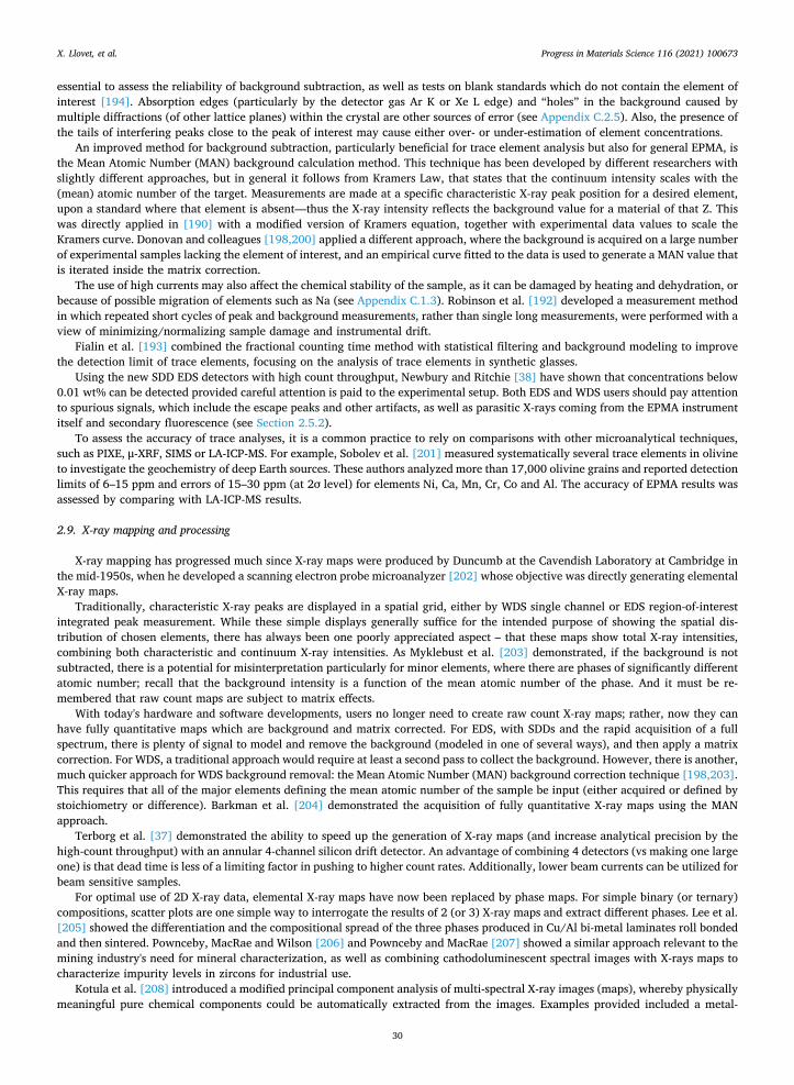
essential to assess the reliability of background subtraction, as well as tests on blank standards which do not contain the element of interest [194]. Absorption edges (particularly by the detector gas Ar K or Xe L edge) and “holes” in the background caused by multiple diffractions (of other lattice planes) within the crystal are other sources of error (see Appendix C.2.5). Also, the presence of the tails of interfering peaks close to the peak of interest may cause either over- or under-estimation of element concentrations.
An improved method for background subtraction, particularly beneficial for trace element analysis but also for general EPMA, is the Mean Atomic Number (MAN) background calculation method. This technique has been developed by different researchers with slightly different approaches, but in general it follows from Kramers Law, that states that the continuum intensity scales with the (mean) atomic number of the target. Measurements are made at a specific characteristic X-ray peak position for a desired element, upon a standard where that element is absent—thus the X-ray intensity reflects the background value for a material of that Z. This was directly applied in [190] with a modified version of Kramers equation, together with experimental data values to scale the Kramers curve. Donovan and colleagues [198,200] applied a different approach, where the background is acquired on a large number of experimental samples lacking the element of interest, and an empirical curve fitted to the data is used to generate a MAN value that is iterated inside the matrix correction.
The use of high currents may also affect the chemical stability of the sample, as it can be damaged by heating and dehydration, or because of possible migration of elements such as Na (see Appendix C.1.3). Robinson et al. [192] developed a measurement method in which repeated short cycles of peak and background measurements, rather than single long measurements, were performed with a view of minimizing/normalizing sample damage and instrumental drift.
Fialin et al. [193] combined the fractional counting time method with statistical filtering and background modeling to improve the detection limit of trace elements, focusing on the analysis of trace elements in synthetic glasses.
Using the new SDD EDS detectors with high count throughput, Newbury and Ritchie [38] have shown that concentrations below 0.01 wt% can be detected provided careful attention is paid to the experimental setup. Both EDS and WDS users should pay attention to spurious signals, which include the escape peaks and other artifacts, as well as parasitic X-rays coming from the EPMA instrument itself and secondary fluorescence (see Section 2.5.2).
To assess the accuracy of trace analyses, it is a common practice to rely on comparisons with other microanalytical techniques, such as PIXE, μ-XRF, SIMS or LA-ICP-MS. For example, Sobolev et al. [201] measured systematically several trace elements in olivine to investigate the geochemistry of deep Earth sources. These authors analyzed more than 17,000 olivine grains and reported detection limits of 6–15 ppm and errors of 15–30 ppm (at 2σ level) for elements Ni, Ca, Mn, Cr, Co and Al. The accuracy of EPMA results was assessed by comparing with LA-ICP-MS results.
2.9. X-ray mapping and processing
X-ray mapping has progressed much since X-ray maps were produced by Duncumb at the Cavendish Laboratory at Cambridge in the mid-1950s, when he developed a scanning electron probe microanalyzer [202] whose objective was directly generating elemental X-ray maps.
Traditionally, characteristic X-ray peaks are displayed in a spatial grid, either by WDS single channel or EDS region-of-interest integrated peak measurement. While these simple displays generally suffice for the intended purpose of showing the spatial dis-tribution of chosen elements, there has always been one poorly appreciated aspect – that these maps show total X-ray intensities, combining both characteristic and continuum X-ray intensities. As Myklebust et al. [203] demonstrated, if the background is not subtracted, there is a potential for misinterpretation particularly for minor elements, where there are phases of significantly different atomic number; recall that the background intensity is a function of the mean atomic number of the phase. And it must be re-membered that raw count maps are subject to matrix effects.
With today's hardware and software developments, users no longer need to create raw count X-ray maps; rather, now they can have fully quantitative maps which are background and matrix corrected. For EDS, with SDDs and the rapid acquisition of a full spectrum, there is plenty of signal to model and remove the background (modeled in one of several ways), and then apply a matrix correction. For WDS, a traditional approach would require at least a second pass to collect the background. However, there is another, much quicker approach for WDS background removal: the Mean Atomic Number (MAN) background correction technique [198,203]. This requires that all of the major elements defining the mean atomic number of the sample be input (either acquired or defined by stoichiometry or difference). Barkman et al. [204] demonstrated the acquisition of fully quantitative X-ray maps using the MAN approach.
Terborg et al. [37] demonstrated the ability to speed up the generation of X-ray maps (and increase analytical precision by the high-count throughput) with an annular 4-channel silicon drift detector. An advantage of combining 4 detectors (vs making one large one) is that dead time is less of a limiting factor in pushing to higher count rates. Additionally, lower beam currents can be utilized for beam sensitive samples.
For optimal use of 2D X-ray data, elemental X-ray maps have now been replaced by phase maps. For simple binary (or ternary) compositions, scatter plots are one simple way to interrogate the results of 2 (or 3) X-ray maps and extract different phases. Lee et al. [205] showed the differentiation and the compositional spread of the three phases produced in Cu/Al bi-metal laminates roll bonded and then sintered. Pownceby, MacRae and Wilson [206] and Pownceby and MacRae [207] showed a similar approach relevant to the mining industry's need for mineral characterization, as well as combining cathodoluminescent spectral images with X-rays maps to characterize impurity levels in zircons for industrial use.
Kotula et al. [208] introduced a modified principal component analysis of multi-spectral X-ray images (maps), whereby physically meaningful pure chemical components could be automatically extracted from the images. Examples provided included a metal-
X. Llovet, et al. Progress in Materials Science 116 (2021) 100673
30
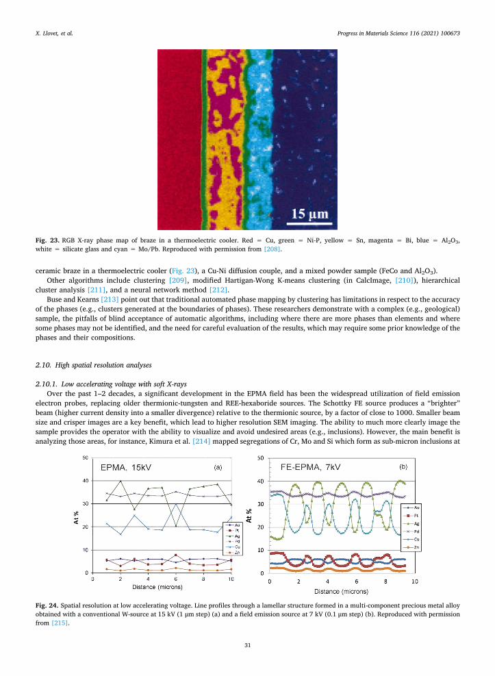
ceramic braze in a thermoelectric cooler (Fig. 23), a Cu-Ni diffusion couple, and a mixed powder sample (FeCo and Al2O3). Other algorithms include clustering [209], modified Hartigan-Wong K-means clustering (in CalcImage, [210]), hierarchical
cluster analysis [211], and a neural network method [212]. Buse and Kearns [213] point out that traditional automated phase mapping by clustering has limitations in respect to the accuracy
of the phases (e.g., clusters generated at the boundaries of phases). These researchers demonstrate with a complex (e.g., geological) sample, the pitfalls of blind acceptance of automatic algorithms, including where there are more phases than elements and where some phases may not be identified, and the need for careful evaluation of the results, which may require some prior knowledge of the phases and their compositions.
2.10. High spatial resolution analyses
2.10.1. Low accelerating voltage with soft X-rays Over the past 1–2 decades, a significant development in the EPMA field has been the widespread utilization of field emission
electron probes, replacing older thermionic-tungsten and REE-hexaboride sources. The Schottky FE source produces a “brighter” beam (higher current density into a smaller divergence) relative to the thermionic source, by a factor of close to 1000. Smaller beam size and crisper images are a key benefit, which lead to higher resolution SEM imaging. The ability to much more clearly image the sample provides the operator with the ability to visualize and avoid undesired areas (e.g., inclusions). However, the main benefit is analyzing those areas, for instance, Kimura et al. [214] mapped segregations of Cr, Mo and Si which form as sub-micron inclusions at
Fig. 23. RGB X-ray phase map of braze in a thermoelectric cooler. Red = Cu, green = Ni-P, yellow = Sn, magenta = Bi, blue = Al2O3, white = silicate glass and cyan = Mo/Pb. Reproduced with permission from [208].
Fig. 24. Spatial resolution at low accelerating voltage. Line profiles through a lamellar structure formed in a multi-component precious metal alloy obtained with a conventional W-source at 15 kV (1 μm step) (a) and a field emission source at 7 kV (0.1 μm step) (b). Reproduced with permission from [215].
X. Llovet, et al. Progress in Materials Science 116 (2021) 100673
31
the grain boundaries of austenitic steel. Susan et al. [215] characterized fine-scale lamellar structures formed in a multi-component precious metal, which were barely discerned using traditional EPMA; important here is also the lower kV used (Fig. 24). These authors also analyzed the weld structure of an austenitic stainless steel showing the improvement in the Ni composition profile when using FE-EPMA.
FE guns can deliver high probe currents in very small diameter probes, even at low accelerating voltages. This is of key im-portance for sub-micron quantitative analysis since at low accelerating voltages (< 10 kV), the X-ray range reduces considerably with the consequent improvement in the spatial resolution. This is illustrated in Table 4, which lists X-ray ranges calculated by using Eq. (1) for Fe Kα (Ec = 7.11 keV) and Fe Lα (Ec = 0.707 keV) X-rays emitted from Fe in pure Fe and trace concentrations of Fe in otherwise pure C, Si, and Au, for incident electron energies in the range from 2.5 to 30 keV. Note that Fe is considered here as a trace element immersed in C, Si, and Au matrices. At 20 keV, the X-ray range for Fe Kα X-rays ranges from 3.9 μm (in C) to 470 nm (in Au), which correspond to the conventional micron-scale spatial resolution. At 2.5 keV, however, the X-ray range of Fe Lα X-rays drops substantially to 123 nm (in C) and to 18 nm (in Au). The improvement in the X-ray range (and therefore in the X-ray spatial resolution) at such low energy is worth noticing.
With conventional thermionic W-based instruments, attempts had been made to work at low voltage with a view toward im-proving the analysis of ultra-light elements and of sub-micron features (see e.g., Willich and Bethke [216]). Pascal et al. [217] reported a successful characterization at 7 kV of sub-micron borides formed at the interface between NiAl and a Ni base superalloy, but the improvements in X-ray imaging achieved by a FE-EPMA on the same material were later showed by Merlet and Llovet [218].
At low accelerating voltage, the effect of the beam size cannot be disregarded when calculating the X-ray spatial resolution (see Section 2.1). The effect of the beam size on the spatial resolution (beam spread) is illustrated in Fig. 25, which shows Monte Carlo simulations of 2D X-ray distributions of Si Kα X-ray emission (corresponding to xz planes integrated over z) and the corresponding radial distributions, generated in Si by 4 keV electron beams with different beam diameters. The radial distributions consist of two main components, a central sharp peak superimposed onto a much broader contribution.
To take into account the effect of the beam size at low voltages, the X-ray spatial resolution R can be written as [3,216]:
= +R R dx , (15)
where Rx is the X-ray range (Eq. (1)) and d is the beam diameter. A more accurate estimate is obtained by considering that both the beam spread and the beam broadening are Gaussian distributions [218]. The formula proposed by Merlet and Llovet is:
= +R R z d4( )x m2 2 (16)
where zm is the depth at which the X-ray depth distribution is maximum. An expression for zm is given e.g., in Merlet [219]. Fournelle et al. [220] demonstrated the good predictions of Eq. (16) compared to experimental EPMA results performed on silicate glass between 800 nm Fe3O4 inclusions. Nevertheless, the accuracy of simple analytical expressions for the determination of the X-ray spatial resolution at low accelerating voltages remains an area of debate [221].
Several studies have devoted efforts to accurately determining the beam diameter in FE-EPMA instruments, since knowledge of this parameter is required to estimate the X-ray spatial resolution at low accelerating voltages. For a prototype FE-electron mi-croprobe, Kimura et al. [222] reported a probe diameter of 40 nm at 10 kV for an electron current of 1 nA, increasing to 200 nm for a 100 nA electron beam. Berger and Nissen [221] measured the beam diameter by using a method described in the ISO/TS24597 standard, reporting values as low as 52 nm for an accelerating voltage of 3 kV and a beam current of 1 nA. Pinard [28] measured the beam diameter of a FE-electron microprobe using the method described by Joy [223] and reported a beam diameter of 52 nm and 107 nm for electron currents of 10 nA and 100 nA, respectively, at 10 kV, in good agreement with the manufacturer’s specifications. However, a steep increase in the beam diameter below 10 kV was observed, reaching a value of 375 nm at 3 kV for an electron current of 100 nA, which leads to an obvious worsening of the lateral resolution. Because of that, a method for the optimization of the
Table 4 X-ray range calculated using Eq. (1) for Fe Kα (Ec = 7.11 keV) and Fe Lα (Ec = 0.707 keV) in pure C, Si, Fe and Au matrices and beam energies in the range 2.5–30 keV.
X. Llovet, et al. Progress in Materials Science 116 (2021) 100673
32
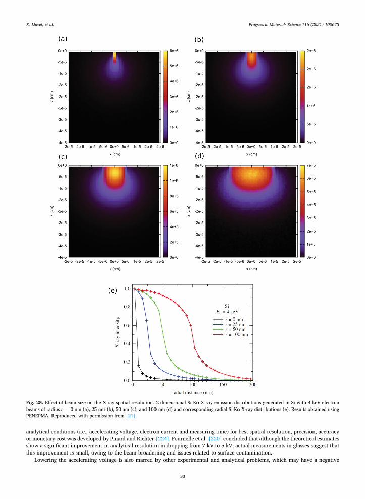
analytical conditions (i.e., accelerating voltage, electron current and measuring time) for best spatial resolution, precision, accuracy or monetary cost was developed by Pinard and Richter [224]. Fournelle et al. [220] concluded that although the theoretical estimates show a significant improvement in analytical resolution in dropping from 7 kV to 5 kV, actual measurements in glasses suggest that this improvement is small, owing to the beam broadening and issues related to surface contamination.
Lowering the accelerating voltage is also marred by other experimental and analytical problems, which may have a negative
Fig. 25. Effect of beam size on the X-ray spatial resolution. 2-dimensional Si Kα X-ray emission distributions generated in Si with 4-keV electron beams of radius r = 0 nm (a), 25 nm (b), 50 nm (c), and 100 nm (d) and corresponding radial Si Kα X-ray distributions (e). Results obtained using PENEPMA. Reproduced with permission from [21].
X. Llovet, et al. Progress in Materials Science 116 (2021) 100673
33
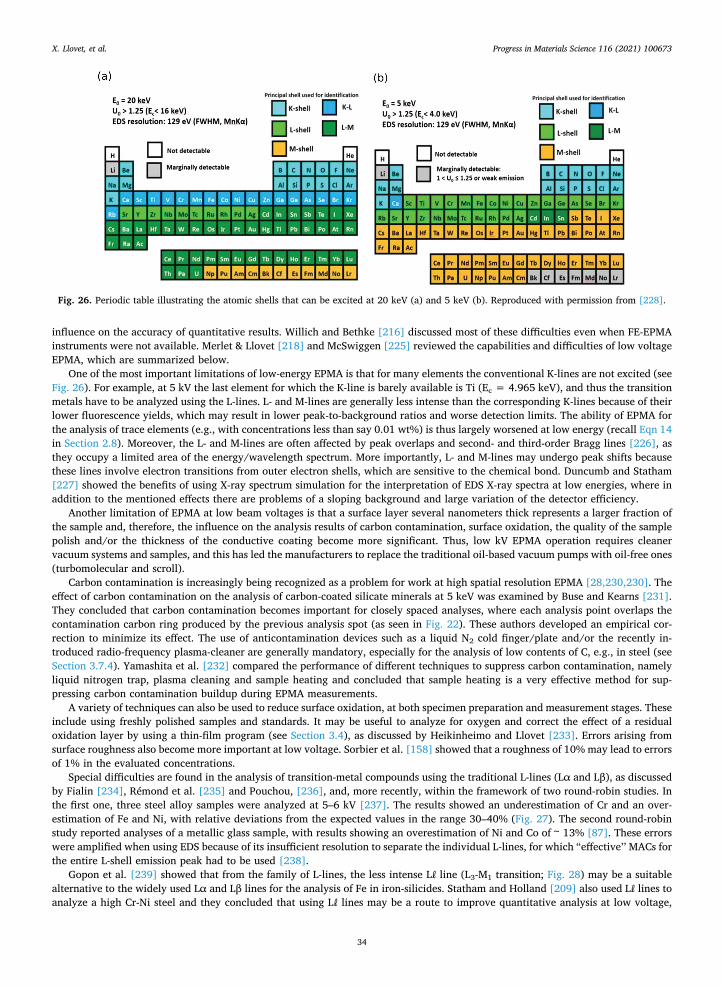
influence on the accuracy of quantitative results. Willich and Bethke [216] discussed most of these difficulties even when FE-EPMA instruments were not available. Merlet & Llovet [218] and McSwiggen [225] reviewed the capabilities and difficulties of low voltage EPMA, which are summarized below.
One of the most important limitations of low-energy EPMA is that for many elements the conventional K-lines are not excited (see Fig. 26). For example, at 5 kV the last element for which the K-line is barely available is Ti (Ec = 4.965 keV), and thus the transition metals have to be analyzed using the L-lines. L- and M-lines are generally less intense than the corresponding K-lines because of their lower fluorescence yields, which may result in lower peak-to-background ratios and worse detection limits. The ability of EPMA for the analysis of trace elements (e.g., with concentrations less than say 0.01 wt%) is thus largely worsened at low energy (recall Eqn 14 in Section 2.8). Moreover, the L- and M-lines are often affected by peak overlaps and second- and third-order Bragg lines [226], as they occupy a limited area of the energy/wavelength spectrum. More importantly, L- and M-lines may undergo peak shifts because these lines involve electron transitions from outer electron shells, which are sensitive to the chemical bond. Duncumb and Statham [227] showed the benefits of using X-ray spectrum simulation for the interpretation of EDS X-ray spectra at low energies, where in addition to the mentioned effects there are problems of a sloping background and large variation of the detector efficiency.
Another limitation of EPMA at low beam voltages is that a surface layer several nanometers thick represents a larger fraction of the sample and, therefore, the influence on the analysis results of carbon contamination, surface oxidation, the quality of the sample polish and/or the thickness of the conductive coating become more significant. Thus, low kV EPMA operation requires cleaner vacuum systems and samples, and this has led the manufacturers to replace the traditional oil-based vacuum pumps with oil-free ones (turbomolecular and scroll).
Carbon contamination is increasingly being recognized as a problem for work at high spatial resolution EPMA [28,230,230]. The effect of carbon contamination on the analysis of carbon-coated silicate minerals at 5 keV was examined by Buse and Kearns [231]. They concluded that carbon contamination becomes important for closely spaced analyses, where each analysis point overlaps the contamination carbon ring produced by the previous analysis spot (as seen in Fig. 22). These authors developed an empirical cor-rection to minimize its effect. The use of anticontamination devices such as a liquid N2 cold finger/plate and/or the recently in-troduced radio-frequency plasma-cleaner are generally mandatory, especially for the analysis of low contents of C, e.g., in steel (see Section 3.7.4). Yamashita et al. [232] compared the performance of different techniques to suppress carbon contamination, namely liquid nitrogen trap, plasma cleaning and sample heating and concluded that sample heating is a very effective method for sup-pressing carbon contamination buildup during EPMA measurements.
A variety of techniques can also be used to reduce surface oxidation, at both specimen preparation and measurement stages. These include using freshly polished samples and standards. It may be useful to analyze for oxygen and correct the effect of a residual oxidation layer by using a thin-film program (see Section 3.4), as discussed by Heikinheimo and Llovet [233]. Errors arising from surface roughness also become more important at low voltage. Sorbier et al. [158] showed that a roughness of 10% may lead to errors of 1% in the evaluated concentrations.
Special difficulties are found in the analysis of transition-metal compounds using the traditional L-lines (Lα and Lβ), as discussed by Fialin [234], Rémond et al. [235] and Pouchou, [236], and, more recently, within the framework of two round-robin studies. In the first one, three steel alloy samples were analyzed at 5–6 kV [237]. The results showed an underestimation of Cr and an over-estimation of Fe and Ni, with relative deviations from the expected values in the range 30–40% (Fig. 27). The second round-robin study reported analyses of a metallic glass sample, with results showing an overestimation of Ni and Co of ~ 13% [87]. These errors were amplified when using EDS because of its insufficient resolution to separate the individual L-lines, for which “effective’’ MACs for the entire L-shell emission peak had to be used [238].
Gopon et al. [239] showed that from the family of L-lines, the less intense Lℓ line (L3-M1 transition; Fig. 28) may be a suitable alternative to the widely used Lα and Lβ lines for the analysis of Fe in iron-silicides. Statham and Holland [209] also used Lℓ lines to analyze a high Cr-Ni steel and they concluded that using Lℓ lines may be a route to improve quantitative analysis at low voltage,
Fig. 26. Periodic table illustrating the atomic shells that can be excited at 20 keV (a) and 5 keV (b). Reproduced with permission from [228].
X. Llovet, et al. Progress in Materials Science 116 (2021) 100673
34
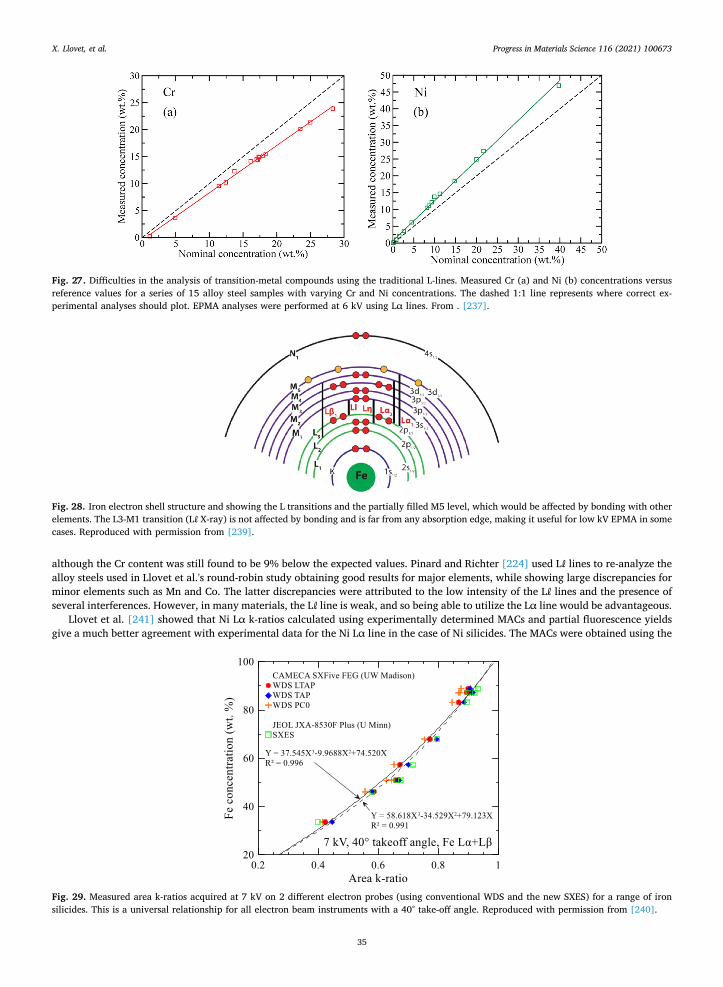
although the Cr content was still found to be 9% below the expected values. Pinard and Richter [224] used Lℓ lines to re-analyze the alloy steels used in Llovet et al.'s round-robin study obtaining good results for major elements, while showing large discrepancies for minor elements such as Mn and Co. The latter discrepancies were attributed to the low intensity of the Lℓ lines and the presence of several interferences. However, in many materials, the Lℓ line is weak, and so being able to utilize the Lα line would be advantageous.
Llovet et al. [241] showed that Ni Lα k-ratios calculated using experimentally determined MACs and partial fluorescence yields give a much better agreement with experimental data for the Ni Lα line in the case of Ni silicides. The MACs were obtained using the
Fig. 27. Difficulties in the analysis of transition-metal compounds using the traditional L-lines. Measured Cr (a) and Ni (b) concentrations versus reference values for a series of 15 alloy steel samples with varying Cr and Ni concentrations. The dashed 1:1 line represents where correct ex-perimental analyses should plot. EPMA analyses were performed at 6 kV using Lα lines. From . [237].
Fig. 28. Iron electron shell structure and showing the L transitions and the partially filled M5 level, which would be affected by bonding with other elements. The L3-M1 transition (Lℓ X-ray) is not affected by bonding and is far from any absorption edge, making it useful for low kV EPMA in some cases. Reproduced with permission from [239].
Fig. 29. Measured area k-ratios acquired at 7 kV on 2 different electron probes (using conventional WDS and the new SXES) for a range of iron silicides. This is a universal relationship for all electron beam instruments with a 40° take-off angle. Reproduced with permission from [240].
X. Llovet, et al. Progress in Materials Science 116 (2021) 100673
35
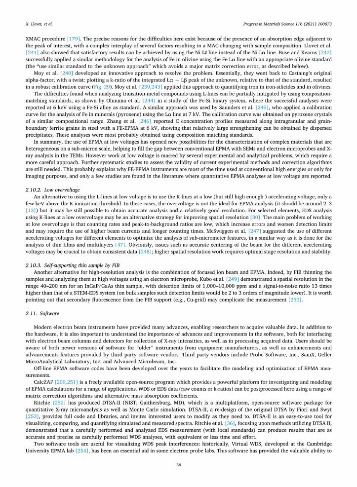
XMAC procedure [179]. The precise reasons for the difficulties here exist because of the presence of an absorption edge adjacent to the peak of interest, with a complex interplay of several factors resulting in a MAC changing with sample composition. Llovet et al. [241] also showed that satisfactory results can be achieved by using the Ni Lℓ line instead of the Ni Lα line. Buse and Kearns [242] successfully applied a similar methodology for the analysis of Fe in olivine using the Fe Lα line with an appropriate olivine standard (the “use similar standard to the unknown approach” which avoids a major matrix correction error, as described below).
Moy et al. [240] developed an innovative approach to resolve the problem. Essentially, they went back to Castaing’s original alpha-factor, with a twist: plotting a k-ratio of the integrated Lα + Lβ peak of the unknown, relative to that of the standard, resulted in a robust calibration curve (Fig. 29). Moy et al. [239,243] applied this approach to quantifying iron in iron-silicides and in olivines.
The difficulties found when analyzing transition-metal compounds using L-lines can be partially mitigated by using composition- matching standards, as shown by Ohnuma et al. [244] in a study of the Fe-Si binary system, where the successful analyses were reported at 6 keV using a Fe-Si alloy as standard. A similar approach was used by Saunders et al. [245], who applied a calibration curve for the analysis of Fe in minerals (pyroxene) using the Lα line at 7 kV. The calibration curve was obtained on pyroxene crystals of a similar compositional range. Zhang et al. [246] reported C concentration profiles measured along intragranular and grain- boundary ferrite grains in steel with a FE-EPMA at 6 kV, showing that relatively large strengthening can be obtained by dispersed precipitates. These analyses were most probably obtained using composition matching standards.
In summary, the use of EPMA at low voltages has opened new possibilities for the characterization of complex materials that are heterogeneous on a sub-micron scale, helping to fill the gap between conventional EPMA with SEMs and electron microprobes and X- ray analysis in the TEMs. However work at low voltage is marred by several experimental and analytical problems, which require a more careful approach. Further systematic studies to assess the validity of current experimental methods and correction algorithms are still needed. This probably explains why FE-EPMA instruments are most of the time used at conventional high energies or only for imaging purposes, and only a few studies are found in the literature where quantitative EPMA analyses at low voltage are reported.
2.10.2. Low overvoltage An alternative to using the L-lines at low voltage is to use the K-lines at a low (but still high enough ) accelerating voltage, only a
few keV above the K ionization threshold. In these cases, the overvoltage is not the ideal for EPMA analysis (it should be around 2–3 [13]) but it may be still possible to obtain accurate analysis and a relatively good resolution. For selected elements, EDS analysis using K-lines at a low overvoltage may be an alternative strategy for improving spatial resolution [30]. The main problem of working at low overvoltage is that counting rates and peak-to-background ratios are low, which increase errors and worsen detection limits and may require the use of higher beam currents and longer counting times. McSwiggen et al. [247] suggested the use of different accelerating voltages for different elements to optimize the analysis of sub-micrometer features, in a similar way as it is done for the analysis of thin films and multilayers [47]. Obviously, issues such as accurate centering of the beam for the different accelerating voltages may be crucial to obtain consistent data [248]; higher spatial resolution work requires optimal stage resolution and stability.
2.10.3. Self-supporting thin sample by FIB Another alternative for high-resolution analysis is the combination of focused ion beam and EPMA. Indeed, by FIB thinning the
samples and analyzing them at high voltages using an electron microprobe, Kubo et al. [249] demonstrated a spatial resolution in the range 40–200 nm for an InGaP/GaAs thin sample, with detection limits of 1,000–10,000 ppm and a signal-to-noise ratio 13 times higher than that of a STEM-EDS system (on bulk samples such detection limits would be 2 to 3 orders of magnitude lower). It is worth pointing out that secondary fluorescence from the FIB support (e.g., Cu-grid) may complicate the measurement [250].
2.11. Software
Modern electron beam instruments have provided many advances, enabling researchers to acquire valuable data. In addition to the hardware, it is also important to understand the importance of advances and improvements in the software, both for interfacing with electron beam columns and detectors for collection of X-ray intensities, as well as in processing acquired data. Users should be aware of both newer versions of software for “older” instruments from equipment manufacturers, as well as enhancements and advancements features provided by third party software vendors. Third party vendors include Probe Software, Inc., SamX, Geller MicroAnalytical Laboratory, Inc. and Advanced Microbeam, Inc.
Off-line EPMA software codes have been developed over the years to facilitate the modeling and optimization of EPMA mea-surements.
CalcZAF [209,251] is a freely available open-source program which provides a powerful platform for investigating and modeling of EPMA calculations for a range of applications. WDS or EDS data (raw counts or k-ratios) can be postprocessed here using a range of matrix correction algorithms and alternative mass absorption coefficients.
Ritchie [252] has produced DTSA-II (NIST, Gaithersburg, MD), which is a multiplatform, open-source software package for quantitative X-ray microanalysis as well as Monte Carlo simulation. DTSA-II, a re-design of the original DTSA by Fiori and Swyt [253], provides full code and libraries, and invites interested users to modify as they need to. DTSA-II is an easy-to-use tool for visualizing, comparing, and quantifying simulated and measured spectra. Ritchie et al. [36], focusing upon methods utilizing DTSA II, demonstrated that a carefully performed and analyzed EDS measurement (with local standards) can produce results that are as accurate and precise as carefully performed WDS analyses, with equivalent or less time and effort.
Two software tools are useful for visualizing WDS peak interferences: historically, Virtual WDS, developed at the Cambridge University EPMA lab [254], has been an essential aid in some electron probe labs. This software has provided the valuable ability to
X. Llovet, et al. Progress in Materials Science 116 (2021) 100673
36
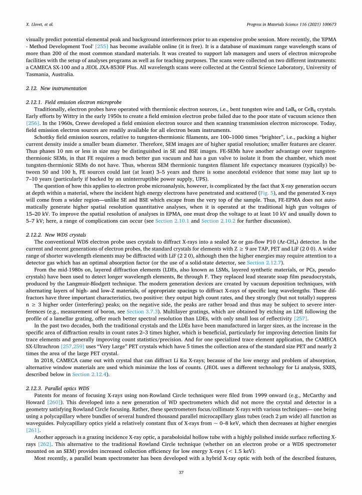
visually predict potential elemental peak and background interferences prior to an expensive probe session. More recently, the 'EPMA - Method Development Tool' [255] has become available online (it is free). It is a database of maximum range wavelength scans of more than 200 of the most common standard materials. It was created to support lab managers and users of electron microprobe facilities with the setup of analyses programs as well as for teaching purposes. The scans were collected on two different instruments: a CAMECA SX-100 and a JEOL JXA-8530F Plus. All wavelength scans were collected at the Central Science Laboratory, University of Tasmania, Australia.
2.12. New instrumentation
2.12.1. Field emission electron microprobe Traditionally, electron probes have operated with thermionic electron sources, i.e., bent tungsten wire and LaB6 or CeB6 crystals.
Early efforts by Wittry in the early 1950s to create a field emission electron probe failed due to the poor state of vacuum science then [256]. In the 1960s, Crewe developed a field emission electron source and then scanning transmission electron microscope. Today, field emission electron sources are readily available for all electron beam instruments.
Schottky field emission sources, relative to tungsten-thermionic filaments, are 100–1000 times “brighter”, i.e., packing a higher current density inside a smaller beam diameter. Therefore, SEM images are of higher spatial resolution; smaller features are clearer. Thus phases 10 nm or less in size may be distinguished in SE and BSE images. FE-SEMs have another advantage over tungsten- thermionic SEMs, in that FE requires a much better gun vacuum and has a gun valve to isolate it from the chamber, which most tungsten-thermionic SEMs do not have. Thus, whereas SEM thermionic tungsten filament life expectancy measures (typically) be-tween 50 and 100 h, FE sources could last (at least) 3–5 years and there is some anecdotal evidence that some may last up to 7–10 years (particularly if backed by an uninterruptible power supply, UPS).
The question of how this applies to electron probe microanalysis, however, is complicated by the fact that X-ray generation occurs at depth within a material, where the incident high energy electrons have penetrated and scattered (Fig. 5), and the generated X-rays will come from a wider region—unlike SE and BSE which escape from the very top of the sample. Thus, FE-EPMA does not auto-matically generate higher spatial resolution quantitative analyses, when it is operated at the traditional high gun voltages of 15–20 kV. To improve the spatial resolution of analyses in EPMA, one must drop the voltage to at least 10 kV and usually down to 5–7 kV; here, a range of complications can occur (see Section 2.10.1 and Section 2.10.2 for further discussion).
2.12.2. New WDS crystals The conventional WDS electron probe uses crystals to diffract X-rays into a sealed Xe or gas-flow P10 (Ar-CH4) detector. In the
current and recent generations of electron probes, the standard crystals for elements with Z ≥ 9 are TAP, PET and LiF (2 0 0). A wider range of shorter wavelength elements may be diffracted with LiF (2 2 0), although then the higher energies may require attention to a detector gas which has an optimal absorption factor (or the use of a solid-state detector, see Section 2.12.7).
From the mid-1980s on, layered diffraction elements (LDEs, also known as LSMs, layered synthetic materials, or PCs, pseudo-crystals) have been used to detect longer wavelength elements, Be through F. They replaced lead stearate soap film pseudocrystals, produced by the Langmuir-Blodgett technique. The modern generation devices are created by vacuum deposition techniques, with alternating layers of high- and low-Z materials, of appropriate spacings to diffract X-rays of specific long wavelengths. These dif-fractors have three important characteristics, two positive: they output high count rates, and they strongly (but not totally) suppress n ≥ 3 higher order (interfering) peaks; on the negative side, the peaks are rather broad and thus may be subject to severe inter-ferences (e.g., measurement of boron, see Section 3.7.3). Multilayer gratings, which are obtained by etching an LDE following the profile of a lamellar grating, offer much better spectral resolution than LDEs, with only small loss of reflectivity [257].
In the past two decades, both the traditional crystals and the LDEs have been manufactured in larger sizes, as the increase in the specific area of diffraction results in count rates 2–3 times higher, which is beneficial, particularly for improving detection limits for trace elements and generally improving count statistics/precision. And for one specialized trace element application, the CAMECA SX-Ultrachron [257,259] uses “Very Large” PET crystals which have 5 times the collection area of the standard size PET and nearly 2 times the area of the large PET crystal.
In 2018, CAMECA came out with crystal that can diffract Li Kα X-rays; because of the low energy and problem of absorption, alternative window materials are used which minimize the loss of counts. (JEOL uses a different technology for Li analysis, SXES, described below in Section 2.12.4).
2.12.3. Parallel optics WDS Patents for means of focusing X-rays using non-Rowland Circle techniques were filed from 1999 onward (e.g., McCarthy and
Howard [260]). This developed into a new generation of WD spectrometers which did not move the crystal and detector in a geometry satisfying Rowland Circle focusing. Rather, these spectrometers focus/collimate X-rays with various techniques— one being using a polycapillary where bundles of several hundred thousand parallel microcapillary glass tubes (each 2 μm wide) all function as waveguides. Polycapillary optics yield a relatively constant flux of X-rays from ~ 0–8 keV, which then decreases at higher energies [261].
Another approach is a grazing incidence X-ray optic, a paraboloidal hollow tube with a highly polished inside surface reflecting X- rays [262]. This alternative to the traditional Rowland Circle technique (whether on an electron probe or a WDS spectrometer mounted on an SEM) provides increased collection efficiency for low energy X-rays (< 1.5 keV).
Most recently, a parallel beam spectrometer has been developed with a hybrid X-ray optic with both of the described features,
X. Llovet, et al. Progress in Materials Science 116 (2021) 100673
37
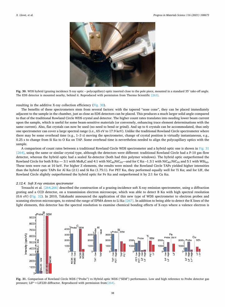
resulting in the additive X-ray collection efficiency (Fig. 30). The benefits of these spectrometers stem from several factors: with the tapered “nose cone”, they can be placed immediately
adjacent to the sample in the chamber, just as close as EDS detectors can be placed. This produces a much larger solid angle compared to that of the traditional Rowland Circle WDS crystal and detector. The higher count rates translates into needing lower beam current upon the sample, which is useful for some beam-sensitive materials (or conversely, enhancing trace element determinations with the same current). Also, flat crystals can now be used (no need to bend or grind). And up to 6 crystals can be accommodated, thus only one spectrometer can cover a large spectral range (i.e., 65 eV to 17.9 keV). Unlike the traditional Rowland Circle spectrometer where there may be some overhead time (e.g., 1–3 s) moving the spectrometer, change of crystal position is virtually instantaneous, e.g., 0.25 s to change from Si Kα to O Kα on TAP. Some overhead time is nevertheless needed to align the polycapillary optics with the sample.
A comparison of count rates between a traditional Rowland Circle WDS spectrometer and a hybrid optic one is shown in Fig. 31 [264], using the same or similar crystal type, although the detectors were different: traditional Rowland Circle had a P-10 gas flow detector, whereas the hybrid optic had a sealed Xe-detector (both had thin polymer windows). The hybrid optic outperformed the Rowland Circle for both B Kα — 3:1 with MoB4C and 4:1 with NiC80NiC95—and for C Kα –1.3:1 with NiC80:NiC95 and 5:1 with WSi60. These tests were run at 10 keV. For higher Z elements, the results were mixed: the Rowland Circle TAPs yielded higher intensities than the hybrid optic TAPs for Al Kα (2:1) and Si Kα (1.75:1). For PET Kα, they performed equally well for Ti Kα; and for LIF, the Rowland Circle slightly outperformed the hybrid optic for Fe Kα and outperformed it by 2:1 for Cu Kα.
2.12.4. Soft X-ray emission spectrometer Terauchi et al. [264,266] described the construction of a grazing-incidence soft X-ray emission spectrometer, using a diffraction
grating and a CCD detector, on a transmission electron microscope, which was able to detect B Kα with high spectral resolution (0.6 eV) (Fig. 32). In 2010, Takahashi announced the application of this new type of WDS spectrometer to electron probes and scanning electron microscopes, to extend the range of EPMA down to Li Kα [267]. In addition to being able to detect the K lines of the light elements, this detector has the spectral resolution to examine chemical bonding effects of X-rays where a valence electron is
Fig. 30. WDS hybrid (grazing incidence X-ray optic – polycapillary) optic inserted close to the pole piece, mounted in a standard 35° take-off angle. The EDS detector is mounted nearby, behind it. Reproduced with permission from Thermo Scientific [263].
Fig. 31. Comparison of Rowland Circle WDS (“Probe”) vs Hybrid optic WDS (“SEM”) performance. Low and high reference to Probe detector gas pressure; LiF*=LiF220 diffractor. Reproduced with permission from[264].
X. Llovet, et al. Progress in Materials Science 116 (2021) 100673
38
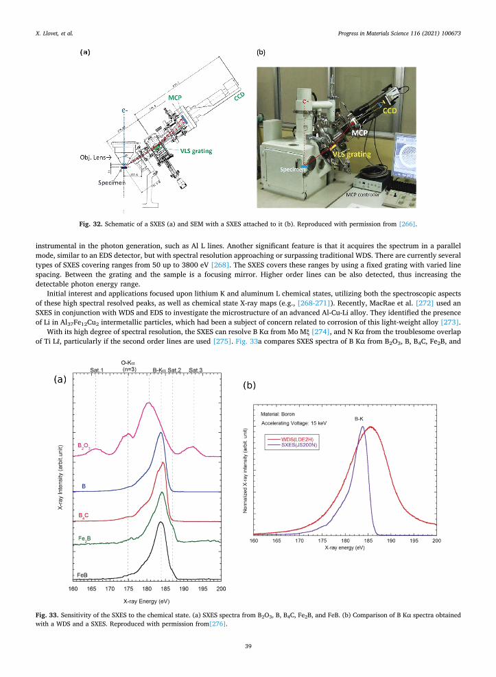
instrumental in the photon generation, such as Al L lines. Another significant feature is that it acquires the spectrum in a parallel mode, similar to an EDS detector, but with spectral resolution approaching or surpassing traditional WDS. There are currently several types of SXES covering ranges from 50 up to 3800 eV [268]. The SXES covers these ranges by using a fixed grating with varied line spacing. Between the grating and the sample is a focusing mirror. Higher order lines can be also detected, thus increasing the detectable photon energy range.
Initial interest and applications focused upon lithium K and aluminum L chemical states, utilizing both the spectroscopic aspects of these high spectral resolved peaks, as well as chemical state X-ray maps (e.g., [268-271]). Recently, MacRae et al. [272] used an SXES in conjunction with WDS and EDS to investigate the microstructure of an advanced Al-Cu-Li alloy. They identified the presence of Li in Al37Fe12Cu2 intermetallic particles, which had been a subject of concern related to corrosion of this light-weight alloy [273].
With its high degree of spectral resolution, the SXES can resolve B Kα from Mo Mξ [274], and N Kα from the troublesome overlap of Ti Lℓ, particularly if the second order lines are used [275]. Fig. 33a compares SXES spectra of B Kα from B2O3, B, B4C, Fe2B, and
Fig. 32. Schematic of a SXES (a) and SEM with a SXES attached to it (b). Reproduced with permission from [266].
Fig. 33. Sensitivity of the SXES to the chemical state. (a) SXES spectra from B2O3, B, B4C, Fe2B, and FeB. (b) Comparison of B Kα spectra obtained with a WDS and a SXES. Reproduced with permission from[276].
X. Llovet, et al. Progress in Materials Science 116 (2021) 100673
39
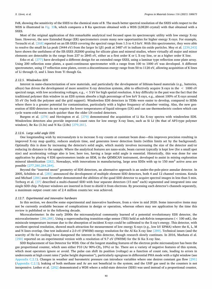
FeB, showing the sensitivity of the SXES to the chemical state of B. The much better spectral resolution of the SXES with respect to the WDS is illustrated in Fig. 33b, which compares a B Kα spectrum obtained with a WDS (LDE2H crystal) with that obtained with a SXES.
Most of the original application of this remarkable analytical tool focused upon its spectroscopic utility with low energy X-ray lines. However, the new Extended Range (ER) spectrometers create many new opportunities for higher energy X-rays. For example, Terauchi et al. [268] reported on an ER-SXES covering the spectral range from 1.5 to 4.3 keV. With this spectrometer, they were able to resolve the small Sn Lα peak (3444 eV) from the larger In Lβ1 peak at 3487 eV in indium tin oxide particles. Moy et al. [239,243] have shown the usefulness of the ER-SXES JS2000 grating for silicate glass and mineral studies, where virtually all major and minor elements are detectable in the range from 237 to 2845 eV, either as a first order K or L X-ray line, or as a higher order K line.
Erko et al. [277] have developed a different design for an extended range SXES, using a laminar type reflection zone plate array. Using 200 reflection zone plates, a quasi-continuous spectrometer with a range from 100 to 1000 eV was developed. A different spectrometer, using 17 reflection zone plates, covers a discontinuous energy range from 50 to 1120 eV, allowing acquisition of K lines of Li through O, and L lines from Ti though Ga.
2.12.5. Windowless EDS Interest in nano-characterization of new materials, and particularly the development of lithium-based materials (e.g., batteries,
alloys) has driven the development of more sensitive X-ray detection systems, able to effectively acquire X-rays in the < 1000 eV spectral range, with low accelerating voltages, e.g., < 5 kV for high spatial resolution. A key difficulty in the past was the fact that the traditional polymer thin window in an EDS system absorbs a high percentage of low keV X-rays, e.g., almost 100% of X-rays around 55 eV (by both the polymer and the grid support). Windowless EDS detectors in TEMs were easier to develop, compared to SEMs where there is a greater potential for contamination, particularly with a higher frequency of chamber venting. Also, the new gen-eration of SDD detectors do not require the lower temperatures of liquid nitrogen (LN) and can use thermoelectric coolers which can cycle warm-cold-warm much quicker than the older LN-cooled detectors.
Burgess et al. [278] and Hovington et al. [279] demonstrated the acquisition of Li Kα X-ray spectra with windowless EDS. Windowless detectors also provide improved count rates for low energy X-ray lines, such as Si Lℓ (8x that of AP3-type polymer window), Be Kα (3.3x) and N Kα (2.8x) [279,281].
2.12.6. Large solid angle EDS One longstanding wish by microanalysts is to increase X-ray counts at constant beam dose—this improves precision resulting in
improved X-ray map quality, reduces analysis time, and generates lower detection limits (within limits set by the background). Optimally this is done by increasing the detector's solid angle, which mainly involves increasing the size of the detector and/or reducing its distance to the sample. Where the analytical features are nano-scale, beam current typically is kept low (for a small spot size) and accelerating voltage also is low; here too, having a large solid angle is essential. Historically, this was done for one application by placing 4 EDS spectrometers inside an SEM, in the QEMSCAN instrument, developed to assist in mining exploration mineral identification [282]. Nowadays, with innovations in manufacturing, large area SDDs with up to 150 mm2 active area are possible [277,280,284,284].
Beyond the “inserted snout” geometry of EDS detectors, an alternative approach is an under-the-pole-piece annular detector. In 2005, Schülein et al. [285] announced the development of multiple element SDD detectors, both 4 and 12 channel versions. Kotula and Michael [286] soon thereafter demonstrated the abilities of the quad SDD detector to acquire spectral images in less than 5 min. Terborg et al. [37] described a multi-channel SDD with four separate detectors (15 mm2 each) segmented and integrated into one single SDD chip. Polymer windows are inserted in front to shield it from electrons. By processing each detector’s channels separately, a maximum output count rate of 2.4 million counts/sec was achieved.
2.12.7. Experimental and innovative hardware In this section, we describe some experimental and innovative hardware, from a view in mid 2020. Some innovative items may
not be currently available because of complications in design or operation, whereas others may see application by the time this review is published or in the following decade.
Microcalorimeter: In the early 2000s the microanalytical community learned of a potential revolutionary EDS detector, the microcalorimeter [286,288]. Using a superconducting transition-edge sensor (TES) held at sub-Kelvin temperatures (< 100 mK), the miniscule temperature increase due to the absorption of incident X-rays could be calibrated to the X-ray's energy. This detector, with excellent spectral resolution, showed much attraction for measurement of low energy X-rays (e.g., low kV EPMA) where the K, L, M and N lines overlap. One test indicated a 2.0 eV (FWHM) energy resolution for the Al Kα X-ray line [289]. Technical issues (and the scarcity of He for cooling) have dampened the interest in this detector, though research slowly continues. In 2016, Maehata el al. [290] reported on an experimental version with a resolution of 9.7 eV (FWHM) for the Si Kα X-ray line.
SDD Replacement of Gas Detector for WDS: One of the longest standing features of the electron probe microanalyzer has been the gas proportional counter, which uses either P10 (Ar 90%-CH4 10%) or Xe. There are a variety of negative features of this system, which most operators ignore or avoid. The pulse can shift its position (voltage) as a function of count rate, leading to errors in undercounts at high count rates (“pulse height depression”), particularly egregious in differential PHA mode with a tight window (see Appendix C.2.1). Changes in weather and barometric pressure can introduce variables where one desires constant gas flow [291] (Appendix C.2.1); leaking of both methane and Ar are not beneficial to the system; and the UHP gas used in the counters is not inexpensive. Lesher et al. [292] demonstrated a WDS where a solid-state detector (SDD) was used instead of a proportional counter,
X. Llovet, et al. Progress in Materials Science 116 (2021) 100673
40
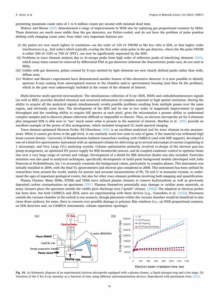
permitting maximum count rates of 1 to 6 million counts per second with minimal dead time. Wuhrer and Moran [293] demonstrated a range of improvements to WDS also by replacing gas proportional counters by SDDs.
These detectors are much more stable than the gas detectors, are Peltier-cooled, and do not have the problem of pulse position shifting with changing count rates. Four other very important features are:
(i) the pulses are now much tighter in resolution—on the order of 129 eV FWHM at Mn Kα—this is EDS, so that higher order interferences (e.g., 2nd order) which typically overlap the first order main pulse in the gas detector, where the Mn pulse FWHM is either 500 eV (LIF) or 750 eV (PET), can now be significantly separated by the SDD.
(ii) Problems in trace element analysis due to Ar-escape peaks from high order of reflection peaks of interfering elements [294], which many times cannot be removed by differential PHA in gas detectors (whereas the characteristic peaks can), do not exist in SDDs.
(iii) Unlike with gas detectors, pulses created by X-rays emitted by light elements are now clearly defined peaks rather than wide, diffuse ones.
(iv) Wuhrer and Moran’s experiments have demonstrated another feature of this alternative detector: it is now possible to identify spurious X-rays coming from unrecognized sources in the chamber and/or spectrometer housing (and then fix the problem), which in the past were unknowingly included in the counts of the element of interest.
Multi-detector multi-spectral microanalysis: The simultaneous collection of X-ray (EDS, WDS) and cathodoluminescence signals (as well as BSE), provides detailed chemical and structural information of complex materials at high spatial resolution. Having the ability to acquire all the analytical signals simultaneously avoids possible problems resulting from multiple passes over the same region, and obviously saves time. The development of the SDD and its one to two order of magnitude improvement in signal throughput and the resulting ability to acquire full spectra at each pixel, gives the microanalyst a greater ability to understand complex samples and to discover phases otherwise difficult or impossible to discern. Thus, an electron microprobe set for 5 elements plus integrated EDS is able now to “see” much easier what is present in the material of interest. MacRae et al. [295] provide an excellent example of the power of this arrangement, which included integrated CL multi-spectral imaging.
Trace-element-optimized Electron Probe: SX-Ultrachron [296] is an excellent analytical tool for trace element in-situ measure-ment. While it cannot get down to the ppb level, it can routinely reach low units to tens of ppms, if the material can withstand high beam current density. University of Massachusetts-Amherst researchers working with CAMECA (and with NSF support), developed a one-of-a-kind five spectrometer instrument with an optimized column for delivering up to several microamps of current (regulating to 1 microamp), and Very Large (VL) analyzing crystals. Column optimization primarily involved re-design of the electron gun/ion pump arrangement, an optimized HV power supply for REE-hexaboride sources, and de-coupled condenser control to optimize beam size over a very large range of current and voltage. Development of a shield for BSE detection diodes was also included. Particular attention was also paid to analytical techniques, specifically development of multi-point background models (developed with John Donovan at ProbeSoftware, Inc.) to accurately constrain the background values, particularly in complex phases. This instrument was initially installed in 2004, with the final VL spectrometers and electron gun completed in 2008. This instrument has been utilized by researchers from around the world, mainly for precise and accurate measurements of Pb, Th and U in monazite crystals, to under-stand the ages of important geological events, but also for other trace element problems involving both mapping and quantification.
Plasma Cleaner: Many SEMs, STEMs and TEMs have utilized plasma cleaners to remove hydrocarbons as well as previously deposited carbon contamination on specimens [297]. Plasmas themselves potentially may damage or oxidize some materials, so many cleaners place the specimen outside the visible glow discharge area (“gentle” cleaner, [298]). The adaption to electron probes has been slow, but both CAMECA and JEOL users are experimenting with these devices (e.g., Yamashita et al. [232]). Placement outside the vacuum chamber in the airlock is one scenario, though placement within the vacuum chamber would be beneficial to also clean those surfaces; for some, there is concern over possible damage to polymer film windows (i.e., on WDS proportional counters, on EDS detectors and, on CAMECA instruments, column separation openings).
Fig. 34. (a) Schematic diagram of an experimental electron microprobe equipped with a plasma cleaner, a liquid nitrogen trap and a hot stage. (b) Variation of the C Kα X-ray intensity as a function of time using different anticontamination devices. Reproduced with permission from [232].
X. Llovet, et al. Progress in Materials Science 116 (2021) 100673
41
Cold stage: Cold stages have been used on some electron beam instruments as far back as the 1970 s, to minimize electron beam damage of biological material, e.g., tissue [299]. Cold stages also “freeze” the hydrocarbons on the surface of samples, so that they do not migrate to the beam impingement region where they are cracked by electrons [229,300].
MacRae et al. [272] described the operation of a LN-cooled sample stage integrated into their field emission electron probe, where an additional benefit is described: the optimization of both low energy X-ray measurement, i.e., Li Kα with the SXES and of CL- imaging.
Hot stage: Yamashita et al. [232] developed a stage which could be heated to 100 °C. This, together with both preliminary plasma cleaning of the specimen as well as within-chamber “gentle” cleaning and use of a LN-cold finger, lead to an improvement in the low- level detection of carbon in steel (Fig. 34). Interestingly, the combined effects seem to be similar to what had been seen three decades before, using an air jet and LN-cold plate [301], though the air jet could have the complicating effect of introducing a gas species which might affect the specimen.
Three-dimensional microanalysis in dual-beam instruments: it is worth mentioning the development of 3D microanalysis in dual- beam instruments (i.e., SEM equipped with both EDS and FIB), which requires more sophisticated quantification methods such as the one recently developed by Burdet et al. [172].
3. Applications in material science
In materials science, EPMA has been extensively used for the study of the microstructure and chemical composition of materials such as metals, alloys, steel, ceramics, glass, coatings, biomaterials, composites and advanced materials, to determine phase diagrams and phase transformations, diffusion profiles, analysis of inclusions and precipitates, failure analysis, oxidation, corrosion and seg-regation phenomena and for the analysis of thin films and coatings. A selection of representative applications of EPMA to materials science and engineering, chosen to show the current merits and limitations of the technique, is discussed below. We cover in some more detail the characterization of materials containing light elements as well as those containing actinide elements.
3.1. Microstructure characterization
The predominant application of EPMA for microstructure characterization is to identify phases observed in the backscattered electron image of the SEM or electron probe. Since the elastic scattering of electrons monotonically increases as a function of the mean atomic number of the material, BSE imaging allows the user to quickly locate compositional differences in the microstructure. This is especially useful to locate a certain phase in a multi-phase microstructure. For example, Fallah-Mehrjardi et al. [302] used BSE images (Fig. 35) to identify the phases in the pyrometallurgical Cu-Fe-O-S-Si system of the copper smelting process. The matte, the phase that will be recovered as part of the smelting process, appears brighter since it has the highest concentration of Cu and Fe in the form of sulphides. The slag also contains Fe and Cu but in lower concentrations in the form of oxides as well as SiO2. It has a lower mean atomic number and thus a lower BSE intensity. Tridymite, the high temperature phase of SiO2, is visible within the slag as the sample was quenched from 1200 °C. Since it has the same chemical composition as the silica crucible, both have the same gray level in spite their different crystal structure. Sub-micrometer copper-rich veins were found in the slag (see Fig. 35a). Measurements of the chemical composition at different locations in the microstructure (e.g., matte close to slag, matte close to gas, etc.) allowed the authors to understand the reactions involved in the copper smelting process and the achieved phase equilibria after different equilibration times. The measured chemical composition was used to calculate ratios between the elements present in the matte and slag (e.g., wt% Cu / [wt% Cu + wt% Fe + wt% Si]) and compare them with calculated ratios from the thermodynamic package FactSage [303]. The ability of EPMA to probe specific locations in the microstructure is the key to understand these processes and constitutes an improvement over previous studies based on bulk wet chemistry.
Another example is the work of Samardzija et al. [304] who investigated the secondary phases of Y-doped BaTiO3 ceramics. While
Fig. 35. Gray-scale intensity BSE contrast is useful in many materials for distinguishing phases. (a) BSE image of matte showing the formation of sub-micrometer copper-rich veins. (b) copper smelting sample in the pyrometallurgical Cu-Fe-O-S-Si system. Reproduced with permission from [302].
X. Llovet, et al. Progress in Materials Science 116 (2021) 100673
42
these phases can be located in the BSE image of a polished sample by their darker appearance (lower Ba content), they are often too small for EPMA. In other words, the X-ray emission volume with the analytical conditions used (i.e., accelerating voltage, beam diameter, etc.) is larger than the size of the phases. To promote coarsening of the microstructure, the authors have heat-treated their samples for 120 h at 1360 °C in air before performing a quantitative analysis to identify them as Y2Ti2O7 and Ba6Ti17O40. Another aim of the study was to determine the solid solubility limit of Y in BaTiO3 with the technological implication in mind that Y doping improves the electrical properties. They were able to measure yttrium concentrations below 0.5 wt% using a PET crystal on their WD spectrometer. Despite the lower intensity of the Y Lα X-ray line relative to the Y Kα, this crystal was selected over the TAP crystal due to “the total reflection effect […] causing an anomalous increase of the background intensity and non-linear background behaviour” with the TAP crystal [304]. To compensate for the lower intensity, a beam current of 50 nA and an acquisition time of 100 s were used. The authors estimated the relative error on the Y concentration to be less than 13%.
While BSE imaging is very useful to locate features in many samples, it has three caveats. First it requires a prior knowledge about the composition of the sample and the distribution of the elements within phases, inclusions, etc. A BSE image might show bright and dark regions, indicating regions with low and high atomic numbers, but it provides no information about which elements are segregated in which regions. Secondly, electron channelling also influences BSE imaging as shown in Fig. 36 [304-307]. While the compositional contrast is typically stronger than the channelling contrast, these two components may complicate the interpretation of BSE imaging. Finally, it is difficult to distinguish features with a similar composition. The brightness and contrast of the BSE detector can be adjusted to enhance small differences but depending on the sample and dynamic range of the detector, it is often impossible to obtain a representative image without saturating the image.
This limitation was observed by Laigo et al. [308] in their analysis of high performance heat resistant steel alloys (high nickel and chromium containing steel with small amount of niobium). They noted that the bright niobium-containing phases could be dis-tinguished easily from the dark grey chromium-rich phases in the BSE images (Fig. 37); however, two different chromium carbides, Cr23C6 and Cr7C3, could not be differentiated. To identify the chromium carbides, the authors used instead two analytical techniques: electron backscatter diffraction and EPMA. Cr23C6 has a face-centered-cubic crystal lattice with a much larger lattice parameter than the austenitic matrix: 10.64 Å ([308]) vs. 3.43 Å ([309]), and Cr7C3 is orthorhombic. The composition of the two carbides is also
Fig. 36. Channelling contrast present in polycrystalline bulk Ni with grains in different orientations; lighter gray indicates higher backscattering, darker lower backscattering. Reproduced with permission from [305].
Fig. 37. BSE image of a high-performance heat resistant steel. Due to the high contrast in atomic number, the bright niobium-containing phases can easily be distinguished from the dark grey chromium-rich phases. Reproduced with permission from [308].
X. Llovet, et al. Progress in Materials Science 116 (2021) 100673
43
significantly different and could be identified by EPMA (Cr23C6: 94 wt% Cr 6 wt% C, and C7C3: 91 wt% Cr and 9 wt% C). Laigo et al. used an electron microprobe equipped with WD spectrometers to determine the composition of several carbides. As detailed in the paper, considerations were taken to (i) adjust the accelerating voltage to 10 kV to decrease the X-ray emission volume, (ii) reduce the influence of peaks interfering with the carbon Kα peak by adjusting the pulse height analyzer parameters and (iii) use a liquid nitrogen cold finger during the measurement to minimize the effect of carbon contamination on the carbon quantification.
The decision of Laigo et al. to use the Cr, Fe and Ni Lα lines for the quantification, especially in combination with the stan-dardization using pure element standards, was understandable – but not 100% correct (see Section 2.10.1). Results from a round- robin inter-laboratory study subsequently published by Llovet et al. [237] reveal large errors when these low energy X-ray lines are used for the quantification of stainless steels when pure element standards are used (Fig. 27). While the concern of X-ray fluorescence of the Cr Kα by Fe and Ni Kα X-rays increasing the X-ray emission volume is legitimate, the round-robin reports an underestimation of the Cr content by up to 17% which could prevent the accurate differentiation between Cr23C6 and Cr7C3. Potential solutions would be, while still measuring the Lα lines, to further reduce the accelerating voltage or to use the standards with a similar composition as the carbides. Pinard and Richter [310] showed good quantification results on Cr23C6 and Fe3C with an accelerating voltage of 3 kV whereas they reported improved quantification results of the stainless steel of the round-robin when a steel with a similar compo-sition is used as the standard. Another solution is to use the Lℓ line instead of the Lα line (see Section 2.10.1).
As did Laigo and co-authors [308], other authors faced the limitations of BSE imaging and complemented the microstructural analysis of their materials with the acquisition of X-ray maps. X-ray maps are typically acquired at a lower resolution than electron images because a longer dwell time per pixel is required to collect enough X-rays. Maps can be acquired by deflecting the electron beam (as SE/BSE images) or by moving the stage. The latter is common for acquisitions with WD spectrometers where spectrometer defocusing influences the X-ray intensity for field of view greater than 30–40 µm. While X-ray maps are still considered qualitative, they are more descriptive than BSE images as each map shows the distribution of an element within the field of view. There is no need to interpret the grayscale of a BSE image nor to have prior knowledge about the sample chemistry to identify regions containing particular element(s). The intensity of each pixel in X-ray maps can either be the raw peak intensity or the net intensity (Section 2.9). The former corresponds to the X-ray intensity measured by a WD spectrometer at a fixed position centered on the X-ray peak; the latter corresponds to the total intensity inside a region of interest of the ED spectrum spanning the X-ray peak. When interpreting “peak intensity” or “window integral” X-ray maps, one should therefore be aware of potential artifacts due to changes in the background intensity and overlapping X-ray peaks (especially, but not exclusively, with EDS). Use of “net intensity” X-ray maps implies the measurement (or calculation using the “Mean Atomic Number” background model [199]) of the background intensity and its subtraction from the peak intensity as well as an interference correction [311] or peak deconvolution procedure to resolve overlapping X-ray peaks.
For example, the B map taken from Chang et al. [312] shows that dark regions in the BSE image correspond to boron-rich
Fig. 38. (b) BSE image and X-ray maps of (c) B, (e) Si and (g) Fe of a Ni-based alloy. Reproduced with permission from [312].
X. Llovet, et al. Progress in Materials Science 116 (2021) 100673
44
inclusions of a Ni-Cr-B-Si alloy. The X-ray map also shows a variation of boron between the grains of the matrix (black and gray regions). A closer inspection of the Fe map shows a lower Fe Kα intensity in the gray regions of the B map (also a lower Si intensity, see Fig. 38). This indicates a higher Ni concentration in these regions and therefore a slightly higher background intensity. Without measuring and correcting the background, it is impossible to conclude from the X-ray maps whether grains of the matrix have different boron concentrations. Instead of net intensity X-ray maps, Chang et al. performed quantitative analyses (background cor-rection implied) in different grains and found a variation of 5 wt% B (see Fig. 5 of their paper), confirming the intensity difference observed in the B map. Furthermore, Chang et al. used a combination of X-ray maps and quantitative analyses to identify the other phases within the microstructure (Ni3Si, Ni3B, CrB and Cr7C3) and to understand the influence of the temperature on the micro-structure. The X-ray maps provided information about their distribution and morphology (e.g., area fraction of certain phases), whereas the quantitative analyses assessed how the atomic ratios between the elements vary at different temperatures.
As have many other researchers, Chang et al. compared their EPMA results with another analytical technique. The additional technique may provide verification of EPMA results (e.g., XRD), different information (e.g., crystallography from TEM/EBSD) or simply lower or higher resolution capabilities (e.g., light optical microscopy or TEM). As stated by Newbury [4], “testing of electron probe microanalysis whenever possible with other techniques was much more common in the early history of the field, and although such independent studies are often difficult, it is important to continue such testing today to ensure the rigor of our analyses”.
In the case of Chang et al. [312], XRD was used to confirm the phase identification performed by EPMA. Both techniques identified the same number of phases. In other publications, the complementary nature of the two techniques was demonstrated, as one technique was used to identify phases that could not be observed or detected by the other technique. As part of their work on potential materials for the cathode of solid oxide fuel cells, Grundy et al. [313] investigated the solid solution of SrO in La2O3 and vice versa. In the La2O3 matrix, the α-La2O3 and β phases could not be distinguished in the optical and electron images of the electron microprobe due to their similar Sr content. The composition of these phases was instead determined by XRD using standards with different Sr content.
Aljarrah et al. [314] studied the Mg-Al-Sr system, a promising system for high temperature application of Mg alloys with good creep resistance. Based on thermodynamic calculations, the presence of Al4Sr in the microstructure was predicted but could not be detected by EPMA. However, XRD measurements confirmed its existence. The authors attributed this discrepancy to the fact that Al4Sr appears in the microstructure as small precipitates, below the achievable resolution of EPMA.
In other cases, EPMA proved to be more insightful than XRD to identify phases. Jiang et al. [315] identified a new phase (Al78Ca9Ni13) in the Al-Ca-Ni system using quantitative point analyses at different locations on BSE images. The phase was later confirmed by a reanalysis of the XRD measurements. In their study of the influence of minor alloying elements on the corrosion resistance of the Mg-9Al alloy, Mingo et al. [316] noted that the alloying addition does not affect the composition or morphology of the two-phase matrix, but Mn, Nd and Y change the composition of the intermetallic compounds. EPMA was able to identify many intermetallic compounds (Al-Mn-Fe, Al-Fe-Nd, Al2Y, etc.) whereas XRD only detected Al2Y. The experimental results of Mingo et al. [316] seem to tie in with the conclusion of Ha et al. [317] in their investigation of the Mo-Si-B system. They attributed the differences between the boron content measured by EPMA and XRD to “the inability of XRD to detect phases in a small volume fraction”. All in all, these examples show the complementarity of EPMA and XRD techniques and their limitations, especially to measure small features and features with a low volume fraction. This is the reason why some authors continued their investigations using trans-mission electron microscopy and atom probe tomography .
An obvious consequence of moving to higher resolution instruments is the reduction of the analyzed volume, from bulk cen-timeter-sized samples to nanometer-sized lamellae or needles. Van Sluytman et al. [318] compared the quantitative results between EPMA and APT in their study on the partitioning of several alloying elements (Al, Ru, Ta, W, Re, Ir and Pt) between the γ and γ’ phases of Ni-based superalloys. Apart from W, both techniques gave similar partitioning coefficients, calculated from the measured atomic fractions of each element in the γ and γ’ phases. The W discrepancy and other smaller differences were attributed to the fact that samples measured by EPMA were homogenized and aged whereas APT needles were extracted directly after homogenization. Based on these results, Van Sluytman et al. evaluated the pros and cons of the two techniques. On one hand, APT has a superior spatial resolution. The EPMA measurements, consisting of at least 10 spot measurements per sample, have larger standard deviations than the APT measurements. The interaction volume was one reason given by the authors to explain the larger variations. Without the raw intensities and acquisition times it is difficult to assess the contribution of the counting statistics to these errors. Nonetheless, the size of the X-ray emission volume and the excitation of the adjacent phase could definitely be a source of error. Reducing the accelerating voltage from 20 kV and increasing the electron dose might have been ways to improve EPMA statistics. On the other hand, the authors mentioned that the APT results are more dependent on the elimination of elemental segregation during the homogenization. As APT samples a smaller volume, any remaining segregation between inter-dendritic and dendritic regions would introduce a bias. Overall, this example shows the complementary nature of the two techniques: EPMA offers a screening method to evaluate potential elemental segregation in the sample, whereas APT provides a quantitative analysis of a particular area at a higher resolution.
Richter et al. [319] performed a similar comparison between quantitative results performed in an electron microprobe equipped with WD spectrometers and TEM equipped with an ED spectrometer in their analysis of the structure of automotive catalytic con-verters. They measured the elemental distribution across two catalytic converters after brazing in order to understand the influence of this elevated-temperature process on the oxidation resistance of catalytic converters. The inter-diffusion and carbide formation of Cr was of particular interest. Although BSE imaging in the electron microprobe identified regions in the braze-influenced area, TEM investigation was required to reveal the finer details of the microstructure. For example, the globular phases identified in the BSE images actually consisted of two phases, which explains the differences between the quantification results of the two techniques. The
X. Llovet, et al. Progress in Materials Science 116 (2021) 100673
45
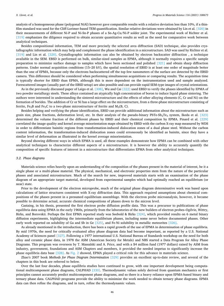
analysis of a homogeneous phase (polygonal NiAl) however gave comparable results with a relative deviation less than 10%, if a thin- film standard was used for the Cliff-Lorimer-based TEM quantification. Similar relative deviations were obtained by Lin et al. [320] in their measurements of different Ni-P and Ni-Sn-P phases of a Sn-Ag-Cu/Ni-P solder joint. The experimental work of Richter et al. [319] emphasizes the diligence required to obtain accurate quantitative results as well as the need for comparative work between analytical techniques.
Besides compositional information, TEM and more precisely the selected area diffraction (SAD) technique, also provides crys-tallographic information which may help and complement the phase identification in a microstructure. SAD was used by Richter et al. [319] and Lin et al. [320]. Crystallographic information can also be obtained by electron backscatter diffraction , a technique available in the SEM. EBSD is performed on bulk, similar-sized samples as EPMA, although it normally requires a specific sample preparation to minimize surface damage to samples which have been sectioned and polished [321] and obtain sharp diffraction patterns. Under normal acquisition conditions (15–20 kV), the spatial resolution of EBSD is at least one order of magnitude better than the one of EPMA, because only the electrons backscattered off the top few nanometers of the surface are detected by the EBSD camera. This difference should be considered when performing simultaneous acquisitions or comparing results. The acquisition time is typically shorter for EBSD than EPMA, although this is more dependent on the instrumentation used and sample analyzed. Forescattered images (usually part of the EBSD setup) are also possible and can provide rapid SEM-type images of crystal orientations.
As in the previously discussed paper of Laigo et al. [308], Wu and Cai [322] used EBSD to verify the phases identified by EPMA of two powder metallurgy steels. These alloys contained an atypically high concentration of boron to induce liquid phase sintering. The authors were interested in understanding the sintered microstructure and the effects of other alloying elements (C, Cr and Ni) on the formation of borides. The addition of Cr or Ni has a large effect on the microstructure, from a three-phase microstructure consisting of ferrite, Fe2B and Fe3C to a two-phase microstructure of ferrite and M3(B, C).
Besides helping and verifying the phase identification, EBSD can provide additional information about the microstructure such as grain size, phase fractions, deformation level, etc. In their analysis of the pseudo-binary PbTe-Sb2Te3 system, Ikeda et al. [323] determined the volume fraction of the different phases by EBSD and their chemical composition by EPMA. Pinard et al. [229] correlated the image quality and kernel average misorientation maps obtained by EBSD with the carbon X-ray map measured by WDS in order to differentiate bainitic regions from transformation-induced dislocation zones of a dual phase steel. Without the carbon content information, the transformation-induced dislocation zones could erroneously be identified as bainite, since they have a similar level of deformation as illustrated in the kernel average misorientation.
Beyond showing different ways in which EPMA is used, all these examples demonstrate how EPMA can be combined with other analytical techniques to characterize different aspects of a microstructure. It is however the ability to accurately quantify the composition of specific features of interest in a microstructure that differentiates EPMA from other analytical techniques.
3.2. Phase diagrams
Materials science relies heavily upon an understanding of the composition of the phases present in the material of interest, be it a single phase or a multi-phase material. The physical, mechanical, and electronic properties stem from the nature of the particular phases and associated microstructure. Much of the search for new, improved materials starts with an examination of the phase diagram of an appropriate target material, developed from experimental samples which had optimally reached an equilibrium (or near) state.
Prior to the development of the electron microprobe, much of the original phase diagram determinative work was based upon calculations of lattice structures consistent with X-ray diffraction data. This approach required assumptions about chemical com-positions of the phases present in a presumed equilibrium assemblage. With the electron probe microanalysis, however, it became possible to determine actual, accurate chemical compositions of phases down to the micron level.
Castaing, in his thesis, presented the first electron probe diffusion profile data. This was a precursor to publications of phase equilibria data using EPMA in the early 1960s, primarily from the laboratories of the new builders of electron probes–Ogilvie, Wittry, Birks, and Borovskii. Perhaps the first EPMA reported study was Seebold & Birks [324], which provided results on 6 metal binary diffusion experiments, highlighting the intermediate equilibrium phases, including some never before documented phases. Other early work reported on solubility of Ga and Sb in Ge [325], and Fe-Ni solubility in metallic meteorites [326].
As already mentioned in the introduction, there has been a rapid growth of the use of EPMA in determination of phase equilibria. By mid 1970s, the need for critically evaluated alloy phase diagram data had become important, as reported by a U.S. National Academy of Sciences panel [327]. Following a 1977 international U.S. National Bureau of Standards workshop on the need for both alloy and ceramic phase data, in 1978 the ASM (American Society for Metals) and NBS started a Data Program for Alloy Phase Diagrams. This program was overseen by T. Massalski and A. Price, and with a $4 million fund (1977 dollars) raised by ASM from industry, government, foundations and ASM Chapters and members, it provided the needed impetus to significantly increase the phase equilibria data base [328]. As Fig. 2 showed, EPMA played a critical role for this advance in materials science.
Zhao’s 2007 book Methods for Phase Diagram Determination [329] provides an excellent up-to-date review, and several of the chapters in this book are referred to below.
Over the last four decades, phase equilibria studies have continued to grow, with one important development being computa-tional multicomponent phase diagrams, CALPHAD [330]. Thermodynamic values solely derived from quantum mechanics or first principles cannot accurately predict multicomponent phase diagrams, and so there is a heavy reliance upon EPMA-based binary and ternary phase data. CALPHAD programs provide the ability to minimize the work needed to obtain ternary phase diagrams. EPMA data can then refine the diagrams, and in turn, refine the thermodynamic values.
X. Llovet, et al. Progress in Materials Science 116 (2021) 100673
46

A traditional approach to phase equilibria study is the use of the diffusion couple, whereby two materials (metal or non-metal, alloy or pure element) are placed in intimate contact and then subjected to some duration of thermal treatment, typically at at-mospheric pressure, to produce solid solutions and intermetallic compounds. This approach is described in detail in Kodentsov et al. [331]. An advancement upon this technique is the diffusion multiple approach, developed and described by Zhao [332]. In the diffusion multiple approach, three or more different blocks of metal are precisely cut and then placed in intimate contact, heated to a desired temperature to promote thermal interdiffusion and resulting, optimally, in local equilibrium phases. This approach provides the benefits of being a great time saver and is an efficient use of raw materials. With several tri-junctions in one mount, isothermal sections of several ternary systems may be evaluated, rather than making and then processing dozens of individual diffusion couples.
Kodentsov et al. [331] provided an excellent summary of the procedures by which EPMA can be utilized to optimize the accuracy of phase equilibria experimental data – not a trivial exercise. These three authors, with decades of experience, provide an important summary for current and future researchers using EPMA for phase equilibria studies. Important aspects of their summary include: (i) comparison of WDS with EDS technique, with the important point being made that with EDS it can be difficult to obtain very accurate compositional information; (ii) sample preparation issues: smearing of material across the interphase interfaces, and etched surfaces (different phase heights); (iii) errors in EPMA measurements: normal errors in counting statistics and in data correction methods (matrix, normalization); (iv) misunderstanding of analytical volume (it is larger than electron spot size)—thus making it impossible to determine the exact compositions at an interface; (v) sample-to-detector geometry: X-ray absorption of the generated X-rays if they are close to and pass through a different adjacent phase (thus, the orientation to specific spectrometer is critical, see Section 2.5.2, Fig. 19); and (vi) possible secondary fluorescence, whereby the primary characteristic and continuum X-rays may excite other phases from tens to up to hundreds of microns away to produce X-rays, “contaminating” the results (e.g., Fournelle et al. [141]). Many times, this will generate high analytical totals, which is another reason not to normalize the analytical wt% totals. The worst cases are for K- K fluorescence for materials with Z > 21 (Sc) and atomic numbers differing by two (e.g., Fe/Ni and Cu/Co).
Some recent examples of the application of EPMA to phase equilibria studies follow. Cao and Zhao [332-335] provide examples of recent phase equilibria studies done by WDS-EPMA. They used a “dual-anneal
diffusion multiple” which combines many diffusion couples and triples, with two thermal treatments. An initial high temperature treatment (1200 °C for 500 h) is followed by an anneal at an intermediate temperature (900, 800, or 700 °C) for 500 h. The first treatment quickly forms solid solutions and intermetallic compounds; the second anneal yields phase precipitation from super-saturated solid solutions. In this example, by combining 5 elements (Cr, Fe, Ni, Co and Mo) in a carefully prepared mount, eight diffusion triples were produced (Fig. 39).
Cao and Zhao [333] considered the important Fe-Cr-Ni phase diagram. The experiments were initially examined by SEM, with BSE imaging and EDS qualitative evaluation. Then the electron microprobe was used to acquire a series of tie-lines by 1 µm steps across many precipitate/matrix interfaces, together with EPMA point analyses along the locations separating the precipitate-bearing and the precipitate-free areas. They found these results to be in good agreement and together they define phase boundaries well.
In this study, the 1200 °C results correlated extremely well with prior published experiments, as well as with ThermoCalc and the TCFES database. The results showed that the bcc to sigma phase transformation occurred initially via a massive transformation mechanism. Experimental Ni solubility at 900 °C in the alpha phase was determined for the first time, and showed that Thermo-Calc slightly under-estimated this (Fig. 40). This study also suggested that in several cases, phase regions computed by Thermo-Calc may not be accurate. A range of other results were found, with the important point being made that it would have taken much more time, materials and effort to produce this using the traditional approach.
Hellstén and Taskinen [336] studied the Cu-O-Al2O3-MgO system in order to better understand MgAl2O4-refractories and slag in non-ferrous smelting. Using WDS-EPMA, they studied the compositions of experimental mixtures over the temperature range of 1100–1400 °C, particularly relevant to copper-making. Oxygen was determined by EPMA. Their experiments showed that the
Fig. 39. (Left) An electrical discharge machining-cut slice of the fabricated diffusion multiple after heat treatment, with a reference figure. (Right) A BSE image of the Cr-Fe-Ni region indicated in the red box in figure at left. This was location of EPMA phase measurements. Reproduced with permission from [333].
X. Llovet, et al. Progress in Materials Science 116 (2021) 100673
47

calculated solubilities (by MTDATA 6.0 and its multiphase module) of Al2O3 and MgO in the oxide liquid phase are much larger than experimentally seen, and that the MgAl2O4 refractory material is chemically resistant to CuOx-rich oxide liquid. This paper is no-teworthy in providing a full description of the EPMA procedure setup (device, kV, current, standards, matrix correction), providing non-normalized wt% data, and analytical errors (standard deviations).
Clearly, accuracy of the determination of the compositions of post-experimental phases is paramount, in terms of the starting components (elements). However, perhaps less well appreciated is the impact of impurities, e.g., O, C, N, H, either present in the starting materials (suppliers cite “metals basis” purity, suggesting that light elements may be present [see Appendix C.3.1]), or acquired from the environment. Also, the presence of an unintentional oxide film at interfacial contact or presence of impurities potentially could hinder nucleation of an expected phase [331].
“The experimentalist should certainly be confident that any impurities in his/her test specimens are not in quantities sufficient to modify meaningful results” (Smith, in Zhao [327], p.19). As is pointed out elsewhere in our review, it is critical that EPMA analytical results are not normalized, as < 100 wt% totals are one valuable indicator of the presence of impurities. Smith (in Zhao [327]) reviews experimental results for the Cu-Nb system, showing that a relatively small amount of unrecognized oxygen contamination could produce an erroneous conclusion.
Another example is provided by Kodentsov et al. [331], in a Nb/Ni couple, where an apparent Nb2Ni phase was upon further examination found to be Nb4Ni2N, resulting from contamination of the starting Nb. They emphasize that there are potential carbides, oxides and nitrides produced in phase equilibria experiments; these may result from either impurities of the starting materials or environmental contamination. Contamination can occur at various steps in the process, and may not be reproducible [337].
Standards-based EPMA offers the ability to decipher a situation such as this, as the non-normalized analytical total points out the existence of a problem, which indicates further attention is called for to achieve the most accurate results.
3.3. Diffusion
Diffusion plays a key role in the kinetics of many microstructural changes that occur during processing of metals, alloys, ceramics, semiconductors, glasses, and polymers. Accurate knowledge of diffusion coefficients is required for a quantitative description of phase transformation processes that are governed by diffusion such as solidification, precipitation and creep deformation. Oxidation, carburization, nitriding, sintering, coating, cladding and joining are industrial processes that are possible due to diffusion.
Diffusion coefficients have been determined experimentally from concentration profiles measured by EPMA on diffusion couple experiments since the 1960′s. Standard metallographic procedures can be used to prepare bulk diffusion couples, with the critical requirement being to prevent smearing across the interphase interfaces. To derive the diffusion coefficients, the concentration profiles are analyzed by means of the Matano-Boltzmann technique [338]. This technique requires the determination of two integrals and one slope from the concentration profile generated during the diffusion reaction. Examples of the determination of diffusion coefficients using EPMA are numerous [338-346]. Information for the phase diagram can also be extracted from the composition profiles (see Section 3.2). Fig. 41 shows an example of a concentration profile obtained for a NiAl-RuAl diffusion couple annealed at 1100 °C for
Fig. 40. 900 °C EPMA determined tie lines and point measurements in the study by Cao and Zhao [333], compared with prior published de-terminations as well as ThermoCalc predictions. Reproduced with permission from [333].
X. Llovet, et al. Progress in Materials Science 116 (2021) 100673
48
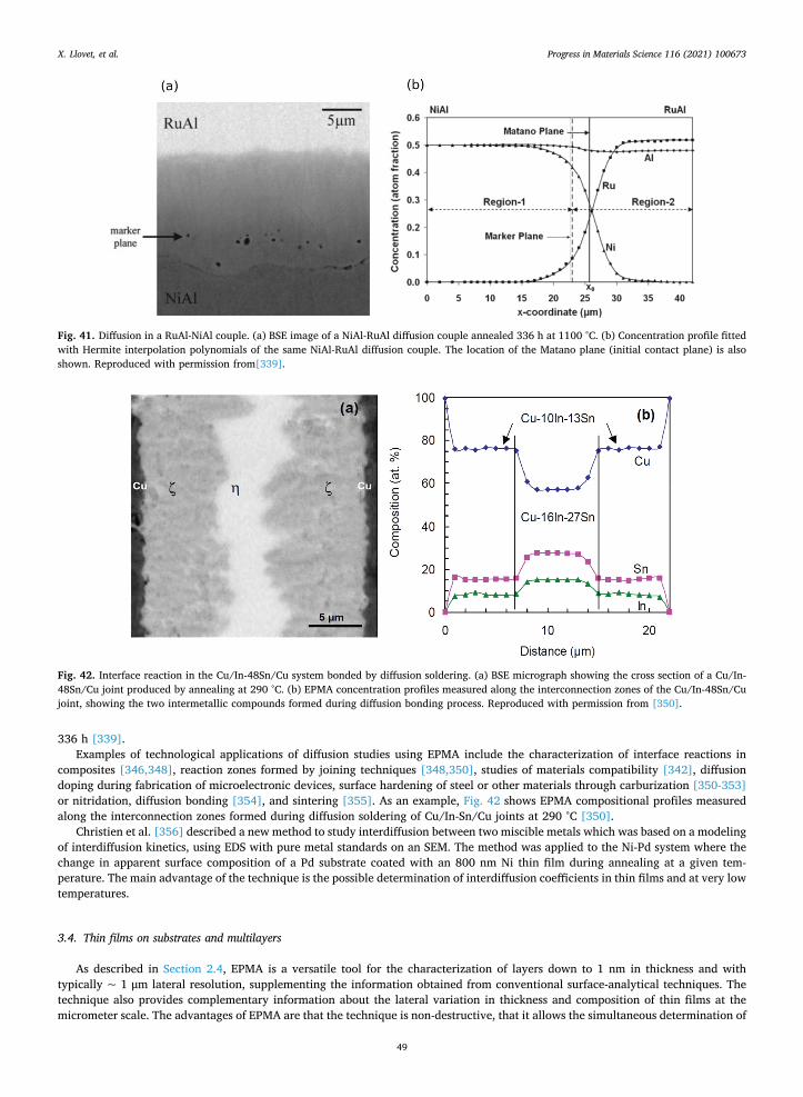
336 h [339]. Examples of technological applications of diffusion studies using EPMA include the characterization of interface reactions in
composites [346,348], reaction zones formed by joining techniques [348,350], studies of materials compatibility [342], diffusion doping during fabrication of microelectronic devices, surface hardening of steel or other materials through carburization [350-353] or nitridation, diffusion bonding [354], and sintering [355]. As an example, Fig. 42 shows EPMA compositional profiles measured along the interconnection zones formed during diffusion soldering of Cu/In-Sn/Cu joints at 290 °C [350].
Christien et al. [356] described a new method to study interdiffusion between two miscible metals which was based on a modeling of interdiffusion kinetics, using EDS with pure metal standards on an SEM. The method was applied to the Ni-Pd system where the change in apparent surface composition of a Pd substrate coated with an 800 nm Ni thin film during annealing at a given tem-perature. The main advantage of the technique is the possible determination of interdiffusion coefficients in thin films and at very low temperatures.
3.4. Thin films on substrates and multilayers
As described in Section 2.4, EPMA is a versatile tool for the characterization of layers down to 1 nm in thickness and with typically ~ 1 μm lateral resolution, supplementing the information obtained from conventional surface-analytical techniques. The technique also provides complementary information about the lateral variation in thickness and composition of thin films at the micrometer scale. The advantages of EPMA are that the technique is non-destructive, that it allows the simultaneous determination of
Fig. 41. Diffusion in a RuAl-NiAl couple. (a) BSE image of a NiAl-RuAl diffusion couple annealed 336 h at 1100 °C. (b) Concentration profile fitted with Hermite interpolation polynomials of the same NiAl-RuAl diffusion couple. The location of the Matano plane (initial contact plane) is also shown. Reproduced with permission from[339].
Fig. 42. Interface reaction in the Cu/In-48Sn/Cu system bonded by diffusion soldering. (a) BSE micrograph showing the cross section of a Cu/In- 48Sn/Cu joint produced by annealing at 290 °C. (b) EPMA concentration profiles measured along the interconnection zones of the Cu/In-48Sn/Cu joint, showing the two intermetallic compounds formed during diffusion bonding process. Reproduced with permission from [350].
X. Llovet, et al. Progress in Materials Science 116 (2021) 100673
49
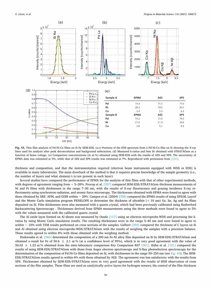
thickness and composition, and that the instrumentation required (electron beam instruments equipped with WDS or EDS) is available in many laboratories. The main drawback of the method is that it requires precise knowledge of the sample geometry (i.e., the number of layers and what element/s is/are present in each layer).
Several studies have compared the performance of EPMA for the analysis of thin films with that of other experimental methods, with degrees of agreement ranging from ~ 5–20%. Procop et al. [357] compared SEM-EDS/STRATAGem thickness measurements of Ni and Pt films with thicknesses in the range 7–30 nm, with the results of X-ray fluorescence and grazing incidence X-ray re-flectometry using synchrotron radiation, and atomic force microscopy. The thicknesses obtained with EPMA were found to agree with those obtained by XRF, AFM, and GIXR within ~ 20%. Campos et al. (2004) [358] compared the EPMA results of using XFILM, Layerf and the Monte Carlo simulation program PENELOPE to determine the thickness of ultrathin (< 10 nm) Ge, Sn, Ag and Au films deposited on Si. Film thicknesses were also measured with a quartz crystal, which had been previously calibrated using Rutherford Backscattering Spectroscopy . Thicknesses derived from EPMA measurements using the three methods were found to agree to 5% with the values measured with the calibrated quartz crystal.
The Al oxide layer formed on Al sheets was measured by Osada [117] using an electron microprobe-WDS and processing the k- ratios by using Monte Carlo simulation results. The resulting thicknesses were in the range 5–40 nm and were found to agree to within ~ 10% with TEM results performed on cross sections of the samples. Galbert [359] compared the thickness of C layers on Si and Al obtained using electron microprobe-WDS/STRATAGem with the results of weighing the samples with a precision balance. These results agreed to within 8% with those obtained with the weighing method.
Hodoroaba et al. [360] determined the composition of a 200 nm Fe-Ni alloy film deposited on Si by SEM-EDS/STRATAGem and obtained a result for Fe of 50.6 ± 2.1 at.% (at a confidence level of 95%), which is in very good agreement with the value of 50.02 ± 1.23 at.% obtained from the inter-laboratory comparison Key Comparison K67 [361]. Kühn et al. [121] compared the results of using SEM-EDS/STRATAGem with those from Auger electron spectroscopy and X-Ray photoelectron spectroscopy for the determination of the composition of Pd-Ni-Co films deposited on Si, with thicknesses in the range 50–250 nm (see Fig. 43). The SEM- EDS/STRATAGem results agreed to within 6% with those obtained by AES. The agreement was less satisfactory with the results from XPS. Thicknesses obtained by SEM-EDS/STRATAGem were in very good agreement with the results of SEM observation of cross sections of the film samples. These films are used as catalytically active layers for hydrogen sensors; the control of the film thickness
Fig. 43. Thin film analysis of Pd-Ni-Co films on Si by SEM-EDS. (a-c) Portions of the EDS spectrum from a Pd-Ni-Co film on Si showing the X-ray lines used for analysis after peak deconvolution and background subtraction. (d) Measured k-ratios and best fit obtained with STRATAGem as a function of beam voltage. (e) Comparison concentrations (in at.%) obtained using SEM-EDS with the results of AES and XPS. The uncertainty of EPMA data was estimated at 5%, while that of AES and XPS results was estimated at 7%. Reproduced with permission from [121].
X. Llovet, et al. Progress in Materials Science 116 (2021) 100673
50
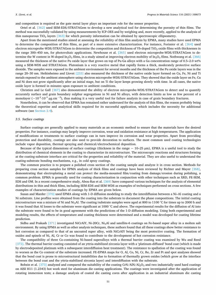
and composition is required as the gate metal layer plays an important role for the sensor properties. Ortel et al. [362] used SEM-EDS/STRATAGem to develop a new analytical tool for determining the porosity of thin films. The
method was successfully validated by using measurements by ICP-OES and by weighing and, more recently, applied to the analysis of thin nanoporous TiO2 layers [363] for which porosity information can be obtained by spectroscopic ellipsometry.
Apart from the mentioned studies aimed at assessing the reliability of thin film analysis by EPMA, many studies have used EPMA to determine the composition of thin films, as part of a more extensive characterization. For instance, Forissier et al. [364] used electron microprobe-WDS/STRATAGem to determine the composition and thickness of Yb-doped TiO2 oxide films with thicknesses in the range 300–450 nm, for photovoltaic applications. Newhouse et al. [365] used electron microprobe-WDS/STRATAGem to de-termine the W content in W-doped In2O3 films, in a study aimed at improving electron mobility of In2O3 films. Nothwang et al. [366] measured the thickness of the native Pu oxide layer that grows on top of Pu-Ga alloys with a Ga concentration range of 0.5–2.0 wt% using a SEM-WDS and STRATAGem. Plutonium is a very reactive metal that rapidly forms a thick, moderately protective surface dioxide. The samples were exposed in the ambient environment for several months and the thickness of the Pu oxide layers was in the range 20–30 nm. Heikinheimo and Llovet [233] also measured the thickness of the native oxide layer formed on Cu, Fe, Ni and Ti metals exposed to the ambient atmosphere using electron microprobe-WDS/STRATAGem. They showed that the oxide layer on Fe, Cu and Ni does not grow significantly after an initial stage, but on Ti the layer keeps growing slowly with time. In all cases, the native oxide layer is formed in minutes upon exposure to ambient conditions.
Christien and Le Gall [367] also demonstrated the ability of electron microprobe-WDS/STRATAGem to detect and to quantify accurately surface and grain boundary sulphur segregations in Ni and Ni alloys, with detection limits as low as few percent of a monolayer (~10-2-10-3 μg.cm−2), thus making it a very useful tool for failure analysis in case of grain boundary fractures.
Nonetheless, it can be observed that EPMA has remained rather underused for the analysis of thin films, the reason probably being the theoretical expertise and analytical skills required for its successful application, which includes the necessity for additional software (see Section 2.4).
3.5. Surface coatings
Surface coatings are generally applied to many materials as an economic method to ensure that the materials have the desired properties. For instance, coatings may largely improve corrosion, wear and oxidation resistance at high temperatures. The application of modifications or treatments to surface coatings can in turn improve its corrosion and wear properties. Apart from providing protection and durability, coatings are also used to provide decoration to surfaces. The most common used coating technologies include vapor deposition, thermal spraying and chemical/electrochemical deposition.
Because of the typical dimensions of surface coatings (thickness in the range ~ 10–25 μm), EPMA is a useful tool to study the distribution of chemical elements in the coating to characterize its microstructure. The microscopic reactions and structures forming at the coating-substrate interface are critical for the properties and reliability of the material. They are also useful to understand the coating-substrate bonding mechanisms, e.g., in cold spray coatings.
The common practice is to prepare a polished cross section of the coating sample and analyze it in cross section. Methods for preparing cross section samples for EPMA analysis of thick films and coatings have been reviewed by Richter and Mayer [368], demonstrating that electroplating a metal can protect the media-mounted film/coating from damage/erosion during polishing, a common problem. EPMA is generally used for coating characterization in conjunction with other techniques such as XRD, FE-SEM, EDS and OM. In a recent comprehensive study, Abou-Ras et al. [369] have compared various techniques for the analysis of elemental distributions in thin and thick films, including SEM-EDS and SEM-WDS as examples of techniques performed on cross sections. A few examples of characterization studies of coatings by EPMA are given below.
Susan and Marder [370] used EPMA along with 1-D diffusion modeling to study the interdiffusion between a Ni–Al coating and a Ni substrate. Line profiles were obtained from the coating into the substrate to document the phase compositions. The initial coating microstructure was a mixture of Ni and Ni3Al. The coating/substrate samples were aged at 800 to 1100 °C for times up to 2000 h and it was found that Al losses to the substrate were significant at 1000 °C and above. The experimental results for the diffusion of Al into the substrate were found to be in good agreement with the predictions of the 1-D diffusion modeling. Using both experimental and modeling results, the effects of temperature and coating thickness were determined and a model was developed for coating lifetime prediction.
Sidhu and Prakash [371] investigated NiCrAlY, Ni-20Cr, Ni3Al and satellite-6 coatings on Fe-based super alloy in a molten salt environment. By using EPMA as well as other analysis techniques, these authors found that all these coatings show better resistance to hot corrosion as compared to that of an uncoated super alloy, with NiCrAlY being the most protective coating. The formation of oxides and spinels of Ni, Al, Cr or Co was found to contribute to the development of hot corrosion resistance.
The compatibility of three Co-containing Ni-based superalloys with a thermal barrier coating was examined by Wu and Reed [372]. The thermal barrier coating consisted of an yttria-stabilized zirconia layer with a ‘platinum-diffused’ bond coat (which is made by electrodeposited platinum with a subsequent interdiffusion heat treatment). The resistance to spallation of the coating was found to worsen as the Co content of the substrate increased. FE-EPMA maps for O, Al, Co, Ni, Cr, Re, Zr and Pt and spot analyses showed that the bond coat is prone to microstructural instabilities due to formation of thermally grown oxides (which grow at the interface between the bond coat and the yttria-stabilized zirconia layer) and interdiffusion with the substrate.
Bobzin et al. [373] analyzed and compared the suitability of the coating CrN/AlN/Al2O3 and two industrially used hard coatings on AISI H11 (1.2343) hot work steel for aluminum die casting applications. The coatings were investigated after the application of rotating immersion tests; a damage analysis of coated die casting cores after application in an industrial aluminum die casting
X. Llovet, et al. Progress in Materials Science 116 (2021) 100673
51
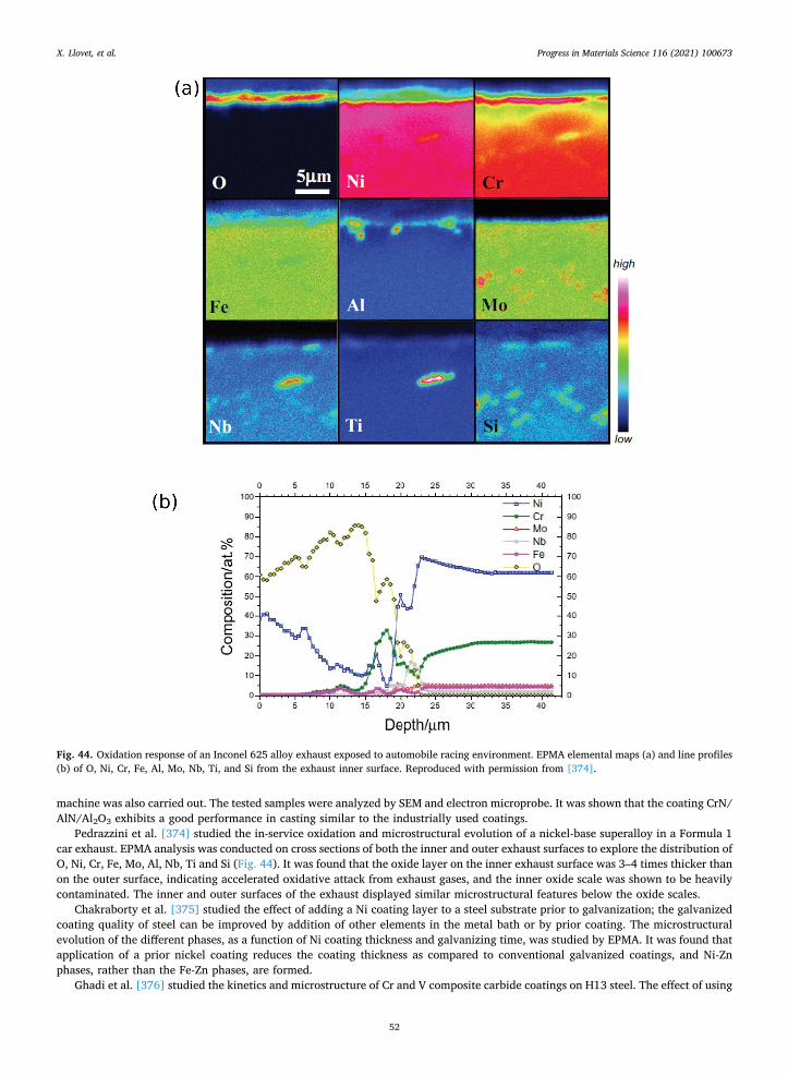
machine was also carried out. The tested samples were analyzed by SEM and electron microprobe. It was shown that the coating CrN/ AlN/Al2O3 exhibits a good performance in casting similar to the industrially used coatings.
Pedrazzini et al. [374] studied the in-service oxidation and microstructural evolution of a nickel-base superalloy in a Formula 1 car exhaust. EPMA analysis was conducted on cross sections of both the inner and outer exhaust surfaces to explore the distribution of O, Ni, Cr, Fe, Mo, Al, Nb, Ti and Si (Fig. 44). It was found that the oxide layer on the inner exhaust surface was 3–4 times thicker than on the outer surface, indicating accelerated oxidative attack from exhaust gases, and the inner oxide scale was shown to be heavily contaminated. The inner and outer surfaces of the exhaust displayed similar microstructural features below the oxide scales.
Chakraborty et al. [375] studied the effect of adding a Ni coating layer to a steel substrate prior to galvanization; the galvanized coating quality of steel can be improved by addition of other elements in the metal bath or by prior coating. The microstructural evolution of the different phases, as a function of Ni coating thickness and galvanizing time, was studied by EPMA. It was found that application of a prior nickel coating reduces the coating thickness as compared to conventional galvanized coatings, and Ni-Zn phases, rather than the Fe-Zn phases, are formed.
Ghadi et al. [376] studied the kinetics and microstructure of Cr and V composite carbide coatings on H13 steel. The effect of using
Fig. 44. Oxidation response of an Inconel 625 alloy exhaust exposed to automobile racing environment. EPMA elemental maps (a) and line profiles (b) of O, Ni, Cr, Fe, Al, Mo, Nb, Ti, and Si from the exhaust inner surface. Reproduced with permission from [374].
X. Llovet, et al. Progress in Materials Science 116 (2021) 100673
52

different Cr and V molar ratios in the metal and oxide baths was analyzed by FE-SEM, XRD, and electron microprobe-WDS, especially regarding the presence of V and Cr-rich regions and Cr and V carbides in the coating. EPMA maps for Cr, V, C and Fe showed that the distribution of Cr carbide-rich regions and V carbide-rich regions become more homogenous with time.
The study of the quality of coatings depending on the coating technology is also a current topic of research in coating technology. Kawaguchi et al. [377] analyzed the quality of coatings obtained by using three thermal spray guns. EPMA analysis allowed a complete elemental characterization of the coatings.
Zhou et al. [378] studied the microstructure, ablation properties and ablation mechanisms of a SiC-ZrC coating on C/C com-posites. EPMA was used to investigate the elemental distribution of Zr, Si and C in the composites and showed that the ZrC is continuous and dense and bonded well with SiC layer. This helps to improve the ablation resistance to the coating.
Jiang et al. [379] studied the hot corrosion performance of a Zr-doped single-phase (Ni,Pt)Al coating in comparison with simple aluminide and normal (Ni,Pt)Al coatings. These authors used EPMA to quantitatively analyze the coating composition and the distribution of elements (Ni, Pt, Al, Cr, O, S and Cl) within the coating after hot corrosion treatment and showed that the hot corrosion resistance of the nickel aluminide coating was notably improved with modification of the Pt and Zr contents (Fig. 45).
The formation and mechanisms of Cr- and Si-enriched glass coating on C steel at high temperatures were investigated by Fu et al. [380]; glass coating is often used to improve the antioxidation ability of C steel. The use of EPMA mappings and line profiles for Fe, Si, Cr and O allowed establishing at which conditions Cr concentrates at the surface, which leads to the formation of an oxide
Fig. 45. Corrosion resistance study of a Pt-modified aluminide coating. BSE image and X-ray maps (a) and concentration profiles (b) of Ni, Pt, Al, Cr, Zr, O, Cl and S from a Zr-doped (Ni,Pt)Al coating deposited on a Ni-based superalloy after a hot corrosion test in Na2SO4/NaCl at 850 °C. The concentration profiles were acquired along the red line shown in the BSE image. The results indicate that the Zr-doped coating shows superior hot corrosion resistance to both conventional aluminide and (Ni,Pt)Al coatings, the enhanced performance being attributed to the interaction of Zr with S and Cl. Reproduced with permission from [379].
Fig. 46. BSE images and X-ray maps of O, Al, Zn and Fe for a 5 wt% Zn-Al coated steel sample after austenitization for (a) 3 min (b) 5 min and (c) 10 min. Reproduced with permission from [381].
X. Llovet, et al. Progress in Materials Science 116 (2021) 100673
53
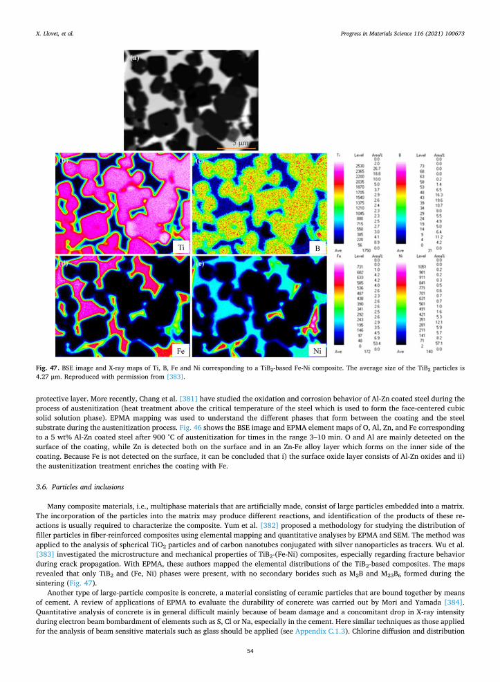
protective layer. More recently, Chang et al. [381] have studied the oxidation and corrosion behavior of Al-Zn coated steel during the process of austenitization (heat treatment above the critical temperature of the steel which is used to form the face-centered cubic solid solution phase). EPMA mapping was used to understand the different phases that form between the coating and the steel substrate during the austenitization process. Fig. 46 shows the BSE image and EPMA element maps of O, Al, Zn, and Fe corresponding to a 5 wt% Al-Zn coated steel after 900 °C of austenitization for times in the range 3–10 min. O and Al are mainly detected on the surface of the coating, while Zn is detected both on the surface and in an Zn-Fe alloy layer which forms on the inner side of the coating. Because Fe is not detected on the surface, it can be concluded that i) the surface oxide layer consists of Al-Zn oxides and ii) the austenitization treatment enriches the coating with Fe.
3.6. Particles and inclusions
Many composite materials, i.e., multiphase materials that are artificially made, consist of large particles embedded into a matrix. The incorporation of the particles into the matrix may produce different reactions, and identification of the products of these re-actions is usually required to characterize the composite. Yum et al. [382] proposed a methodology for studying the distribution of filler particles in fiber-reinforced composites using elemental mapping and quantitative analyses by EPMA and SEM. The method was applied to the analysis of spherical TiO2 particles and of carbon nanotubes conjugated with silver nanoparticles as tracers. Wu et al. [383] investigated the microstructure and mechanical properties of TiB2-(Fe-Ni) composites, especially regarding fracture behavior during crack propagation. With EPMA, these authors mapped the elemental distributions of the TiB2-based composites. The maps revealed that only TiB2 and (Fe, Ni) phases were present, with no secondary borides such as M2B and M23B6 formed during the sintering (Fig. 47).
Another type of large-particle composite is concrete, a material consisting of ceramic particles that are bound together by means of cement. A review of applications of EPMA to evaluate the durability of concrete was carried out by Mori and Yamada [384]. Quantitative analysis of concrete is in general difficult mainly because of beam damage and a concomitant drop in X-ray intensity during electron beam bombardment of elements such as S, Cl or Na, especially in the cement. Here similar techniques as those applied for the analysis of beam sensitive materials such as glass should be applied (see Appendix C.1.3). Chlorine diffusion and distribution
Fig. 47. BSE image and X-ray maps of Ti, B, Fe and Ni corresponding to a TiB2-based Fe-Ni composite. The average size of the TiB2 particles is 4.27 μm. Reproduced with permission from [383].
X. Llovet, et al. Progress in Materials Science 116 (2021) 100673
54
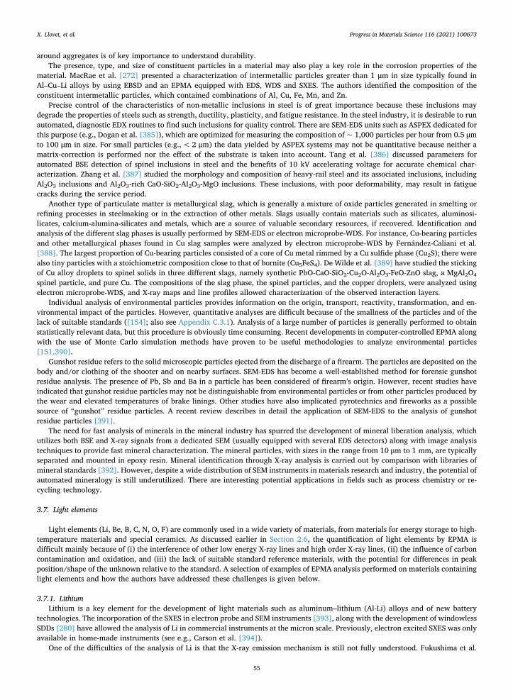
around aggregates is of key importance to understand durability. The presence, type, and size of constituent particles in a material may also play a key role in the corrosion properties of the
material. MacRae et al. [272] presented a characterization of intermetallic particles greater than 1 μm in size typically found in Al–Cu–Li alloys by using EBSD and an EPMA equipped with EDS, WDS and SXES. The authors identified the composition of the constituent intermetallic particles, which contained combinations of Al, Cu, Fe, Mn, and Zn.
Precise control of the characteristics of non-metallic inclusions in steel is of great importance because these inclusions may degrade the properties of steels such as strength, ductility, plasticity, and fatigue resistance. In the steel industry, it is desirable to run automated, diagnostic EDX routines to find such inclusions for quality control. There are SEM-EDS units such as ASPEX dedicated for this purpose (e.g., Dogan et al. [385]), which are optimized for measuring the composition of ~ 1,000 particles per hour from 0.5 μm to 100 μm in size. For small particles (e.g., < 2 μm) the data yielded by ASPEX systems may not be quantitative because neither a matrix-correction is performed nor the effect of the substrate is taken into account. Tang et al. [386] discussed parameters for automated BSE detection of spinel inclusions in steel and the benefits of 10 kV accelerating voltage for accurate chemical char-acterization. Zhang et al. [387] studied the morphology and composition of heavy-rail steel and its associated inclusions, including Al2O3 inclusions and Al2O3-rich CaO-SiO2-Al2O3-MgO inclusions. These inclusions, with poor deformability, may result in fatigue cracks during the service period.
Another type of particulate matter is metallurgical slag, which is generally a mixture of oxide particles generated in smelting or refining processes in steelmaking or in the extraction of other metals. Slags usually contain materials such as silicates, aluminosi-licates, calcium-alumina-silicates and metals, which are a source of valuable secondary resources, if recovered. Identification and analysis of the different slag phases is usually performed by SEM-EDS or electron microprobe-WDS. For instance, Cu-bearing particles and other metallurgical phases found in Cu slag samples were analyzed by electron microprobe-WDS by Fernández-Caliani et al. [388]. The largest proportion of Cu-bearing particles consisted of a core of Cu metal rimmed by a Cu sulfide phase (Cu2S); there were also tiny particles with a stoichiometric composition close to that of bornite (Cu5FeS4). De Wilde et al. [389] have studied the sticking of Cu alloy droplets to spinel solids in three different slags, namely synthetic PbO-CaO-SiO2-Cu2O-Al2O3-FeO-ZnO slag, a MgAl2O4
spinel particle, and pure Cu. The compositions of the slag phase, the spinel particles, and the copper droplets, were analyzed using electron microprobe-WDS, and X-ray maps and line profiles allowed characterization of the observed interaction layers.
Individual analysis of environmental particles provides information on the origin, transport, reactivity, transformation, and en-vironmental impact of the particles. However, quantitative analyses are difficult because of the smallness of the particles and of the lack of suitable standards ([154]; also see Appendix C.3.1). Analysis of a large number of particles is generally performed to obtain statistically relevant data, but this procedure is obviously time consuming. Recent developments in computer-controlled EPMA along with the use of Monte Carlo simulation methods have proven to be useful methodologies to analyze environmental particles [151,390].
Gunshot residue refers to the solid microscopic particles ejected from the discharge of a firearm. The particles are deposited on the body and/or clothing of the shooter and on nearby surfaces. SEM-EDS has become a well-established method for forensic gunshot residue analysis. The presence of Pb, Sb and Ba in a particle has been considered of firearm’s origin. However, recent studies have indicated that gunshot residue particles may not be distinguishable from environmental particles or from other particles produced by the wear and elevated temperatures of brake linings. Other studies have also implicated pyrotechnics and fireworks as a possible source of “gunshot” residue particles. A recent review describes in detail the application of SEM-EDS to the analysis of gunshot residue particles [391].
The need for fast analysis of minerals in the mineral industry has spurred the development of mineral liberation analysis, which utilizes both BSE and X-ray signals from a dedicated SEM (usually equipped with several EDS detectors) along with image analysis techniques to provide fast mineral characterization. The mineral particles, with sizes in the range from 10 μm to 1 mm, are typically separated and mounted in epoxy resin. Mineral identification through X-ray analysis is carried out by comparison with libraries of mineral standards [392]. However, despite a wide distribution of SEM instruments in materials research and industry, the potential of automated mineralogy is still underutilized. There are interesting potential applications in fields such as process chemistry or re-cycling technology.
3.7. Light elements
Light elements (Li, Be, B, C, N, O, F) are commonly used in a wide variety of materials, from materials for energy storage to high- temperature materials and special ceramics. As discussed earlier in Section 2.6, the quantification of light elements by EPMA is difficult mainly because of (i) the interference of other low energy X-ray lines and high order X-ray lines, (ii) the influence of carbon contamination and oxidation, and (iii) the lack of suitable standard reference materials, with the potential for differences in peak position/shape of the unknown relative to the standard. A selection of examples of EPMA analysis performed on materials containing light elements and how the authors have addressed these challenges is given below.
3.7.1. Lithium Lithium is a key element for the development of light materials such as aluminum–lithium (Al-Li) alloys and of new battery
technologies. The incorporation of the SXES in electron probe and SEM instruments [393], along with the development of windowless SDDs [280] have allowed the analysis of Li in commercial instruments at the micron scale. Previously, electron excited SXES was only available in home-made instruments (see e.g., Carson et al. [394]).
One of the difficulties of the analysis of Li is that the X-ray emission mechanism is still not fully understood. Fukushima et al.
X. Llovet, et al. Progress in Materials Science 116 (2021) 100673
55
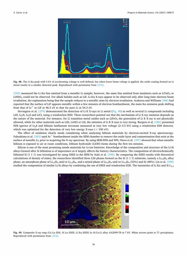
[395] measured the Li Kα line emitted from a metallic Li sample; however, the same line emitted from insulators such as LiTaO3 or LiNbO3 could not be observed. For alkali halides such as LiF, Li Kα X-rays appear to be observed only after long-time electron beam irradiation, the explanation being that the sample reduces to a metallic state by electron irradiation. Arakawa and Williams [396] had reported that the surface of LiF appears metallic within a few minutes of electron bombardment, the main Kα emission peak shifting from that of Li+ in LiF at 46.5 eV to that for pure Li at 54.3 eV.
Hovington et al. [279] demonstrated the detection of Li K X-rays in Li metal (Fig. 48) as well as several Li compounds including LiH, Li3N, Li2S and LiCl, using a windowless SDD. These researchers pointed out that the mechanism of Li X-ray emission depends on the nature of the material. For instance, for Li transition metal oxides such as LiFeO2 the generation of Li K X-ray is not physically allowed, while for other materials such as LiSi, LiAlO or LiS, the emission of Li K X-rays is very strong. Burgess et al. [280] presented EDS spectra of Li2S and lithium lanthanum zirconate measured at very low voltage (2–3.5 kV) using a windowless EDS detector, which was optimized for the detection of very low energy X-rays (< 100 eV).
The effect of oxidation clearly needs considering when analyzing lithium materials by electron-excited X-ray spectroscopy. Fukushima et al. [393] used Ar+ bombardment inside the SEM chamber to remove the oxide layer and contamination that exist at the surface of metallic Li, prior to acquiring the X-ray spectrum. By using SEM-EDS and XPS, Otero et al. [397] showed that when metallic lithium is exposed to air at room conditions, lithium hydroxide (LiOH) forms during the first ten minutes.
Silicon is one of the most promising anode materials for Li-ion batteries. Knowledge of the composition and structure of the Li-Si alloys formed after Si lithiation is of importance as it largely affects the battery characteristics. The composition of electrochemically lithiated Si (1 1 1) was investigated by using SXES in the SEM by Aoki et al. [398]. By comparing the SXES results with theoretical calculations of density of states, the researchers identified three LiSi phases formed on the Si (1 1 1) substrate, namely a Li15Si4 alloy phase, an amorphous phase of Li15Si4 and/or Li13Si4, and a mixed phase of Li15Si4 and/or Li13Si4 (52%) and Si (48%). Lin et al. [399] studied the composition of similar Li-Si alloys by combining the use of SXES and windowless EDS. The intensities of Li Kα and Si L2,3
Fig. 48. The Li Kα peak with 5 kV of accelerating voltage is well defined, but when lower beam voltage is applied, the oxide coating formed on Li metal results in a smaller detected peak. Reproduced with permission from [279].
Fig. 49. Composite X-ray map (Cu Lα EDS, Al Lα SXES, Li Kα SXES) in Al-Cu-Li alloy AA2099-T8 at 7 kV. White arrows point to T1 precipitates. Reproduced with permission from [272].
X. Llovet, et al. Progress in Materials Science 116 (2021) 100673
56
peaks were obtained after deconvolution of the windowless EDS spectra. The Li Kα, Si L2,3, and Si Kα intensities revealed a clear layered structure with varied Li concentrations.
MacRae et al. [272] used an electron microprobe equipped with SXES to analyze the microstructure of the Al–Cu–Li alloy AA2099-T8. The SXES revealed the presence of Li in some constituent intermetallic particles and an Al map obtained with the SXES showed an Al-enriched (i.e., Cu, Li-depleted) zone in the grain boundary network (Fig. 49).
Robbes et al. [400] presented lithium measurements performed on a sample of LiF and on Li3Al5Cu (i.e., 9.5 wt% Li) samples using a specially developed electron microprobe-WDS crystal. The diffracting crystal specifications were not specified and, to the authors’ knowledge, no further information is available regarding this analysis of Li by Rowland Circle WDS.
3.7.2. Beryllium With its excellent thermal and nuclear properties, beryllium is widely used in the nuclear field as well as for x-ray windows for
various detectors. However, it is subject to corrosion, as well as contamination from when the metal is rolled into very thin sheets for use as detector window material (e.g., embedded tiny Fe particles flaked off from steel rollers: [163]).
Mallinson [401] examined corrosion in S-65 Be, using a range of techniques. EDS could not provide the necessary detection of Be; however, Mallinson demonstrated that, coupled with low (5 kV) accelerating voltage (reducing the extent of absorption, as well as providing a smaller interaction volume) the hybrid X-ray optic using an MoB4C layered synthetic diffractor (2d spacing of 200 Å), was well suited for identifying both Be present inside of intermetallic contaminant phases, as well as a Be3N2 second phase particle.
3.7.3. Boron Boron is widely used in materials such as high-temperature devices and lightweight reinforcing fillers, because of its high
hardness and melting point. In their analysis of Mo-Si-B alloys, typically used for high-temperature applications, Fournelle et al. [402], Ha et al. [317] and
Kellner et al. [403] discussed the interference of the Mo Mξ X-ray line with the B Kα X-ray line, where the tail of the Mo Mξ peak extends below the B Kα peak. Fournelle et al. [402] showed the critical importance for a robust (within the matrix correction) interference correction [311] and also demonstrated the easy potential for error by PHA pulse height depression (see Appendix C.2.1). If PHA conditions are improperly applied, incorrect counts on a boron metal standard (commonly used) will lead to over-estimation of boron content: rather than using the same current on a boron metal standard as upon the unknown, beam current on the standard must be set to give the same count rate on the standard as observed for boron on the unknown.
Portebois et al. [404] demonstrated the use of a WDS spectrometer with a 200 Å layered diffractor mounted on a FE-SEM and summarized the issues which must be overcome to correctly determine B concentration in niobium silicide composite phases. These issues are: (i) overlapping X-ray lines (i.e., Nb Mξ), (ii) chemical bonding effects on peak position/shape differences between standard (s) and unknowns, (iii) large potential error due to large absorption correction, and (iv) possible impact of surface contamination. As many of the phases are small (~1 µm wide), and also the absorption path length needed to be minimized to reduce possible error in the absorption correction, the accelerating voltage used was 10 kV (beam current was 17nA). Monte Carlo electron simulations showed that at 10 kV, borides as small as ~ 0.7 μm wide may be analyzed. A liquid nitrogen trap was used to minimize hydrocarbon deposition (and error) at the beam site. Recognizing the well-known impact of differences in peak position/shape due to chemical bonding, pure boron was not used as the B Kα reference material, rather 3 borides were carefully synthesized, and then after acquiring peak wavescans of the possible standards as well as unknowns, appropriate standards were selected. Additionally, a z( )matrix correction, the XPP model of Pouchou and Pichoir [51], was used. In the quantitative analysis, boron was measured by WDS and the other elements by EDS, with published compositions given as non-normalized wt%, so that a composition total close to 100 wt% resulted, demonstrating a high-quality chemical analysis.
The difficulty of measuring boron by EPMA was also discussed by Ruiz Vargas et al. [405]. These authors analyzed the different borides formed in a brazed MC2 Ni-based superalloy by both SEM-EDS and SEM-WDS and concluded that, because of the large errors, measuring boron directly by EDS and WDS may lead to a misinterpretation of the boride nature and a wrong description of the mechanisms controlling the boride's formation during the brazing process. Instead, by accurately measuring the rest of elements, they proposed that it is possible to quantify boron by difference with a precision of 5 at.%. The authors of this PMS review emphasize that this approach must be the very last option used, given the large potential for error.
Given the range of difficulties with accurate determination of boron by EPMA, there are publications that document various approaches (such as the above), which the authors of this review suggest are not the most robust. Besides the unpublished calibration method by Ha et al. [317], another example is the study of Kellner et al. [403]. The latter authors made use of the hybrid optic WDS spectrometer for determination of boron in Mo-Si-B alloys. They used a 5-kV accelerating voltage to evaluate the solubility of B in the Moss, Mo3Si, and Mo5SiB2 phases using the NiC80 diffractor. With the lack of a built-in interference correction, they developed a correction method based on measurements on a reference Mo5SiB2 standard. The high-energy background position is experimentally determined by adjusting the position until the quantification results match the nominal composition of the standard. According to the authors this also corrects for the contribution of the Mo Mξ to the B Kα X-ray intensity, but they later mention that an additional correction is applied based on a normalization to the nominal composition of Mo5SiB2. The universality of this method is unclear.
There is now a new WDS spectrometer which eliminates many (if not all) of the interferences upon the boron Kα peak, the SXES. Liu et al. [274] demonstrated that the spectral resolution of the new SXES has ushered in the ability to clearly separate measurement of boron from the M-line interferences of Mo, as shown in Fig. 50.
X. Llovet, et al. Progress in Materials Science 116 (2021) 100673
57
3.7.4. Carbon Carbon is an important component of many materials widely used in technology. Since the first modifications of the electron
microprobe aimed at allowing carbon analysis [407], EPMA has been widely used for the measurement of C at the micron scale in different materials including steel [229,408-413], metal carbides [179,301,414-420], iron-carbon alloys [419,422], coal [423], graphite and diamonds [424]. Diffusion studies of carbon in a variety of materials have also been carried out with EPMA owing to its micron-size spatial resolution (see Fig. 51) [425] (see also [350,426]).
As for other light elements, second or third order reflections (n > 1 term in Bragg’s law) of X-ray lines from heavier elements present in the sample may overlap with the C Kα line or with the traditional positions where the background is measured. Common examples are related to the measurement of carbon in steel, where the Fe Lβ9 3rd order, Mn Lℓ and Lη 2nd order, Cr Lα, Lℓ and Lη 2nd order, and Ni Lα 3rd order of reflection are located near the C Kα line [28,301,427]. Bächer et al. [428] also report the interference of the Nd Mγ, Mα and Mξ lines with the C Kα line for their analysis of the microstructure of permanent magnet Nd-Fe-B alloy with TiC addition. Operating the pulse height analyzer in differential mode with a small energy window only partially suppresses these high order lines [223,429,430]. Gas counters do not have a very good energy resolution; therefore they cannot completely filter out the low energy C Kα X-rays from the higher energy X-rays from the high order lines of the other alloying elements.
Another challenge of the analysis of C by EPMA is the lack of suitable (i.e., homogeneous) standards. Saunders et al. [176] developed a standard of cementite (Fe3C), which is a line compound that can be produced by carburising pure iron under carefully controlled conditions.
Low contents of C in steel are generally analyzed using the calibration curve method [427,431]. The calibration curve is obtained on reference samples having similar composition to the sample of interest and different carbon contents. This technique has also been used to analyze other elements such as N [430] or Mn [432] in steel. By using the calibration curve, neither a background subtraction nor a matrix correction is required since conversion of the X-ray intensity into concentration is carried out directly by assuming a linear relationship between X-ray intensity and concentration. Pinard et al. [229] used a modified version of the calibration curve technique, in which background is measured on a pure Fe sample and a full matrix correction is performed for all elements, to analyse low C contents in steel.
Fig. 50. With the (wide range) SXES, using the JS300N grating, the B Kα and Mo Mξ peaks are clearly separated. Here, Moss shows no noticeable boron solubility, and two other phases (T2 and Mo2B) show no interference by the Mo Mξ peak [406]. .
Fig. 51. (Left) SEM and C Kα maps of ferrite-martensite dual phase (DP) steels. (Right) Distribution profiles acquired with a field emission electron microprobe-WDS at 15 kV, 100nA and 300 nm step size. Reproduced with permission from [425].
X. Llovet, et al. Progress in Materials Science 116 (2021) 100673
58
As mentioned earlier (Section 2.6) carbon contamination of surfaces within electron beam systems is a long-standing problem. While this is true particularly of older systems with oil-based vacuum pumps, today's oil-free vacuum pumps have not stopped the problem. The presence of insidious adventitious carbon remains; regardless of attempts at keeping surfaces clean and free of organics, the environment is full of it and it resides on the materials going into the SEM and electron probe, where the beam cracks the hydrocarbons. Analysis of carbon can be then difficult. Also, some X-rays may be more heavily absorbed by the C contamination layer. A particularly difficult situation is the acquisition of long wavescans (minutes) where the beam must remain stationary on the same spot.
To minimize carbon contamination the electron microprobe has been traditionally equipped with one or several anti-con-tamination devices such as a liquid nitrogen cold plate or cold finger placed close to the specimen and an air (optimally oxygen) jet [431]. More recently, plasma cleaners have become available in electron-beam instruments and have been used to remove carbon contamination, as shown by Yamashita et al. [232]. The same researchers have shown that heating the sample inside the instrument can also reduce/eliminate carbon buildup under the beam. Tanaka et al. [433] showed that carbon contamination builds up not only while the electron beam is on the sample, it also continues to grow even when the beam is blanked. This explains the increment of contamination observed in line and/or map analyses. Specimen heating appears to have a significant contamination inhibition effect, if coupled with a chamber cold trap [28].
3.7.5. Nitrogen The addition of nitrogen to steel is known to improve many of its properties. For example, nitrogen plays an important role on the
pitting resistance of duplex stainless steel. With a bulk concentration in the range 0.1–0.4 wt%, N is not distributed homogeneously in the ferrite and austenite phases. Moreno et al. [430] used EPMA to determine the partition coefficient of N (ratio of the N contents in ferrite to that in austenite) in highly-alloyed duplex stainless steels. They confirmed that a saturation level (0.03–0.05 wt%) is achieved in the ferrite phase, as it happens in standard duplex stainless steel grades. Measurements were performed using a 95 Å 2d Ni/C multilayer crystal. A critical issue here was the strong curvature of the background and the relatively small N Kα peak (Fig. 52); this precluded the normal linear extrapolation background model. One possible approach here would be to use the “Mean Atomic Number” background model [198,200]. Moreno et al. used a calibration curve, both to deal with the background issue, and also to deal with the trace level of nitrogen. It is common to use a calibration curve to quantify low contents of carbon in steel, and this was the approach used here, calibrating with 5 stainless steels with low nitrogen contents (2 industrial alloys, 3 experimental alloys). A critical consideration is that these five materials all have similar atomic numbers. Three conditions were implemented: (i) LN anti- contamination plate and gas jet to reduce surface carbon contamination which could produce errors in the nitrogen X-ray intensities (high absorption by the carbon), and using the reflected light microscope, obvious beam contamination areas avoided; (ii) lower electron beam energy (10 keV) to reduce the electron penetration and thus reduce the path length of the emergent N Kα X-rays and thus their absorption; (iii) higher electron beam current (200nA) to improve the counting statistics and thus improve the precision of the measurements. As mentioned previously, despite using a careful, tight PHA window, higher (2nd) order of diffraction Fe L lines are not totally removed; this was not a problem here, but is a fact that microanalysts should note. The researchers were able to show the nitrogen contents of the austenite (0.52 to 0.77 wt% N) versus the low content in the ferrite (in most cases below the 0.045 wt% detection limit) of the 4 duplex stainless steels studied.
Other examples of N analysis include that of an oxidized TiN foil, which was examined at 5 keV with a hybrid optic WDS spectrometer [434]. Metal nitrides such as TiN are finding increasing usage as supercapacitors, which combine the functions of capacitors with that of batteries. The Ti L X-ray interferences are well recognized in EPMA. In this case, the Ti Lα and Lβ lines are clearly separated from the N Kα line; the Ti Lℓ line, though cannot be resolved.
Von der Handt and Dalou [435] and Mosenfelder et al. [436] reported on quantifying nitrogen in silicate glasses, giving a detailed EPMA procedure, which included operating at 10 kV and 150nA with two LDE1 (2d spacing of 60 Å) monochromators, with an exponential background model. They reported a detection limit of 0.04 wt% “with reasonable analysis time”.
Fig. 52. (Left) With the complication of determining the N Kα net X-ray intensity due to the curved background at the low sin(θ) position with the 95 Å multilayer, only a curved background model will produce accurate results. (Right) The researchers created a calibration curve from 5 reference alloys (both industrial alloys as well as some prepared in their laboratory). Adapted with permission from [430].
X. Llovet, et al. Progress in Materials Science 116 (2021) 100673
59
3.7.6. Oxygen Analysis of oxygen by EPMA has its own challenges, based upon the proclivity of metals to develop thin oxide coatings. Goldstein
et al. [437] described an analytical method to measure and subtract the background for oxygen from reactive metals or their alloys where a native oxide skin or oxygen-containing surface layer develops and applied it to the measurement of Ti-Si-O compounds where the determination of oxygen in certain phases (e.g., Ti5Si3 and the β-Ti) was of particular interest.
Borrel [438] measured concentration profiles of oxygen in Zircaloy-4 sheet coupons. The research team used in an oil-free FE electron microprobe-WDS vacuum system with a cryo-anti-contamination plate. Oxygen was measured with a PC0 (2d spacing of 45 Å) pseudocrystal, using an exponential background model to correctly model the curved background. A synthetic Fe3O4 crystal was used as a standard, and the PHA was set in differential mode. The complication of the inherent development of an oxide coating upon the polished mounted specimen, leading to inaccuracy in EPMA quantification, was taken into account by means of a blank correction. By acquiring both 5 and 15 kV X-ray data upon the experimentally unreacted base zircalloy, STRATAGem thin film software indicated that the measured O Kα intensity on the unreacted zircalloy was consistent with a 5 nm ZrO2 film. With this information, a blank correction (using Probe for EPMA software) allowed the correction of the 15 kV O Kα counts due to surface oxidation, and the analytical totals approached the proper level of ~ 100 wt%.
3.7.7. Fluorine Fluoride compounds have compelling advantages which make them ideal materials for specific optical applications. A crystal of
BaCaBO3F, a new laser material with potential for self-frequency doubling, was grown by the Czochralski method and was examined by EPMA (15 kV, 15 nA, PAP matrix correction) [439]. The researchers attempted to measure the associated boron directly but that proved unsuccessful (the measured boron content was found to be inaccurate, with too low values), so boron was included in the matrix correction assuming stoichiometry. They reported an elemental abundance of F as 6.94 wt%; the normalized composition of Ba1.04Ca0.96B0.99O3F0.96 compared well with the ideal composition of BaCaBO3F.
3.8. Nuclear materials
One very active branch of the materials sciences is dedicated to the nuclear industry. The increase of interest in the nuclear field for defense or power applications was accompanied by numerous projects dedicated to the investigations of the behavior of new materials for the nuclear industry. Given the expertise of one of the authors of this review, we have focused upon the application of EPMA to nuclear materials which provides a challenging case example.
3.8.1. Nuclear fuel Over the years, and over the generations of nuclear power reactors, different types of fuels have been used. The most common
fuels used nowadays for power production are uranium dioxide fuel (UO2) and mixed oxide fuel [(U,Pu)O2]. Extensive studies of the behavior of the nuclear fuels under different irradiation conditions are conducted in order to extend the burn-up of the fuel, thus, reducing the fuel cycle cost and minimizing the amount of spent fuel. Since the beginning, the electron microprobe has been a tool of primary interest in the study of the fuels, but the instrument requires shielding to avoid radiation exposure of the probe operator and radiation damage of the instrument (see Section 2.7 for more details). Most of the studies require high beam probe currents (100–250 nA) to perform analysis.
The microstructural characterization of the irradiated fuel is of great importance because it is one of the main limiting factors in the utilization of nuclear power reactors. When the local burn-up of the fuel reaches a certain limit and when the local temperature of the fuel is not high enough, the fuel grains in the outer region of the fuel pellet begin to recrystallize and form what is called the high burn-up structure. This structure is made of small grains (~0.15 μm) and a high concentration of 1–2 μm pores. Because of its particular structure, fission gases can be released in the free volume of the rod and can affect its behavior in the nuclear core. The structure of high burn-up fuel pellets has been extensively examined by EPMA [438,441]. The radial distributions of Xe, Cs, Nd, Pu and U is usually measured and used to determine the local burn-up experienced by the fuel pellet. Walker [68,440] has used EPMA profiles of Xe distribution to obtain a measure of its radial extent in the pellet which is of particular interest in the understanding of the fuel behavior.
Extending the burn-up behavior of the nuclear fuel is not the only way to increase its performance. Dopants can also be added to the fresh fuel to optimize the core management. Chromia (Cr2O3) can be used as a dopant in light water reactors to increase the fission gas retention and to improve the pellet cladding interaction behavior. However, non-dissolved Cr precipitates and forms large particles of Cr2O3 on the grain boundaries which can then have negative effects on the fission gas release. Kuri et al. [442] have acquired EPMA elemental X-ray maps and quantitative traverses of fresh Cr-doped UO2 fuel pellets in order to identify chromia precipitates. Large Cr precipitates (≥2 µm) were found and their analysis reveals that they have a composition very close to Cr2O3.
Gd is also used as a dopant as its high neutron capture cross section (for thermal neutrons) helps reduce the excess of reactivity of the fresh fuel assemblies. However, gadolinia doped UO2 fuels have a reduced thermal conductivity which can, because of the higher temperature of the fuel, lead to a higher fractional release of fission gas. As shown before, to improve the retention of fission gas, Cr can be added to the fuel. Cardinaels et al. [443] have studied the microscopic structure of co-doped (U1−x−yGdxCry)O2 fuel and compared the results with single doped (U1−xGdx)O2 fuels. The elements Gd, Cr, U and O were measured by EPMA. However, because of an interference of the O Kα X-ray line (525 eV) by the Cr Lα X-ray line (573 eV), the authors did not try to quantify O directly. They found that co-doped fuel develops a much larger grain size compared to the single doped fuel. But in the co-doped fuel, the solubility of chromia is much lower than in pure UO2 which can precipitate in chromia clusters and cause the same behavior
X. Llovet, et al. Progress in Materials Science 116 (2021) 100673
60
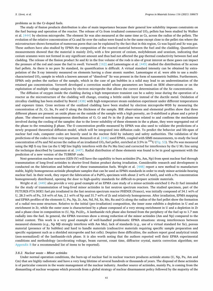
problems as in the Cr-doped fuels. The study of fission products distribution is also of main importance because their general low solubility imposes constraints on
the fuel burnup and operation of the reactor. The release of Cs from irradiated commercial UO2 pellets has been studied by Walker et al. [444] by electron microprobe. The element Xe was also measured at the same time as Cs, across the radius of the pellets. The evolution of the relative concentration of Cs and Xe over the radius were found to be the same except close to the pellet rim where the microstructure shows formation of numerous pores that can be explained by the fact that in this region, Cs was liquid and Xe was gas. These authors have also studied by EPMA the composition of the reacted material between the fuel and the cladding. Quantitative measurements showed that the material is mainly ZrO2 with a few percent of cesium, molybdenum and uranium, indicating that cesium uranates were not formed in any significant amount and thus had not affected the gap thermal conductivity between fuel and cladding. The release of the fission product Xe and Kr in the free volume of the rods is also of great interest as these gases can impact the pressure of the rod and cause the fuel to swell. Verwerft [162] and Lamontagne et al. [445] studied the distribution of Xe across fuel pellets. As there is no pure Xe standard, its quantification is difficult. A virtual standard intensity can be obtained by extra-polation of the X-ray intensity measured on elements having a close atomic number. Lamontagne et al. were able to use a multi- characterized UO2 sample in which a known amount of “dissolved” Xe was present in the form of nanometric bubbles. Furthermore, EPMA only probes the surface of the sample, which in the case of gas bubbles in a solid may lead to an underestimation of the retained gas concentration. Verwerft developed a correction model whose parameters are based on SEM observations or on the exploitation of multiple voltage analyses by electron microprobe that allows the correct determination of the Xe concentration.
The diffusion of oxygen inside the cladding during a high temperature transient can be a safety issue during the operation of a reactor as the microstructure of the cladding will change, creating a brittle oxide layer instead of the ductile metal. Oxidation of zircalloy cladding has been studied by Borrel [438] with high-temperature steam oxidation experiment under different temperatures and exposure times. Cross sections of the oxidized cladding have been studied by electron microprobe-WDS by measuring the concentration of Zr, Cr, Sn, Fe and O along the thickness of the sample. BSE observations and elemental profiles show that three different phases are present: an oxide phase on the outside of the sample with a high porosity, an O-stabilized α phase and a prior-β phase. The observed non-homogeneous distribution of O, Cr and Fe in the β phase was related to and confirms the mechanisms involved during the cooling of the samples: due to the lower solubility of these elements in the α phase, they were segregated out of the phase to the remaining β phase. The O concentration profile measured by EPMA was also used to validate the predictions of a newly proposed theoretical diffusion model, which will be integrated into diffusion code. To predict the behavior and life-span of nuclear fuel rods, computer codes are heavily used in the nuclear field by industry and safety authorities. The validation of the predictions of the codes is thus very important. Botazzoli et al. [446] used EPMA, coupled with SIMS measurements, to study the local concentration of Pu and Nd across the radius of an irradiated UO2 fuel pellet, enriched at 3.5% in 235U (Fig. 53). The Pu was measured using the Mβ X-ray line (as the U Mβ line highly interferes with the Pu Mα line) and corrected for interference by the U Mγ line using the technique described by Lassmann et al. [447]. Radial distribution of these elements was found to be in good agreement with the prediction of a new version of the TUBRNP code.
Next-generation nuclear reactors (GEN-IV) will have the capability to burn actinides (Pu, Am, Np) from spent nuclear fuel through transmutation of long-lived actinides to shorter-lived fission product during irradiation. Considerable research and development is conducted on the fabrication and behavior of these transmutation fuels. Wright et al. [448] report a new method to manufacture stable, highly homogeneous actinide phosphate samples that can be used as EPMA standards in order to study minor-actinide-bearing nuclear fuel. In their work, they report the fabrication of a PuPO4 specimen with about 2 wt% of AmO2 and with a Pu concentration homogeneously distributed, opening the door to high-quality standards for difficult-to-prepare actinide materials.
Wright et al. [449] also provide a very good example of an EPMA case study of a minor-actinide-enriched U-Pu-Zr fuel intended for the study of transmutation of long-lived minor actinides in fast neutron spectrum reactors. The studied specimen, part of the FUTURIX-FTA DOE1 fuel pin irradiated in the fast neutron spectrum reactor PHENIX (France), was initially composed of 34.1 wt% of U, 28.3 wt% of Pu, 3.8 wt% of Am, 2.1 wt% of Np and 31.7 wt% of Zr and relatively homogeneous. After irradiation, EPMA mapping and EPMA profiles of the elements U, Pu, Np, Zr, Am, Nd, Pd, Xe, Mo, Ru and Cs along the radius of the fuel pellet show the formation of a radial two-zone structure. Relative to the initial (pre-irradiation) composition, the inner zone exhibits a depletion in U and an enrichment in Zr, while the outer zone is characterized by a phase composed of a very strong enrichment in U and a depletion in Zr and a phase close in composition to (U, Np, Pu)Zr2. A lanthanide rich phase also formed from the periphery of the fuel up to 1.7 mm radially into the fuel. In general, the EPMA traverses show a strong reduction of the minor actinides (Am and Np) compared to the initial content. This work is a very good example of well-handled problematic EPMA situations: strong interferences between measured elements (e.g., Np Mβ strongly interferes with Am Mα), lack of standards (e.g., use of a virtual standard for Xe), porous material (presence of Xe bubbles) and hard to handle materials (radioactive materials requiring specific sample preparation and specific equipment such as a shielded microprobe and hot cells). Despites these difficulties, the authors report good analytical totals (non-normalized) of the lanthanide-rich phase. It is also worth noting that the authors reported well their EPMA experimental conditions and methodology (accelerating voltage, beam current, count time, diffractor crystal, matrix correction algorithm; see Appendix B for a recommended list of items to be reported).
3.8.2. Nuclear waste – Minor actinides Under normal operation conditions, the burn-up of nuclear fuel in nuclear reactors produces actinide atoms (U, Np, Pu, Am and
Cm) that are highly radiotoxic and have a very long lifetime of several hundreds or thousands of years. The disposal of these actinides is of particular concern in the waste management of the nuclear industry. Another source of actinides, mainly Pu, is coming from the dismantling of nuclear weapons which proceeds from a global strategy of nuclear disarmament policy followed by the majority of the
X. Llovet, et al. Progress in Materials Science 116 (2021) 100673
61
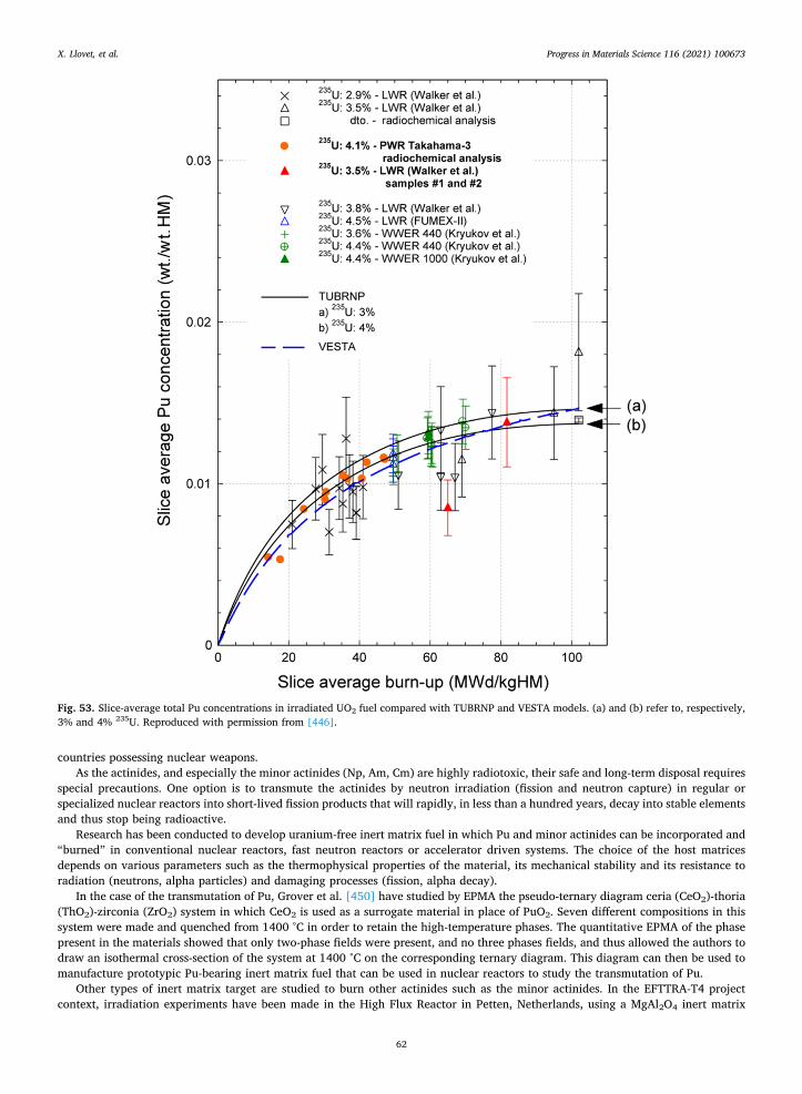
countries possessing nuclear weapons. As the actinides, and especially the minor actinides (Np, Am, Cm) are highly radiotoxic, their safe and long-term disposal requires
special precautions. One option is to transmute the actinides by neutron irradiation (fission and neutron capture) in regular or specialized nuclear reactors into short-lived fission products that will rapidly, in less than a hundred years, decay into stable elements and thus stop being radioactive.
Research has been conducted to develop uranium-free inert matrix fuel in which Pu and minor actinides can be incorporated and “burned” in conventional nuclear reactors, fast neutron reactors or accelerator driven systems. The choice of the host matrices depends on various parameters such as the thermophysical properties of the material, its mechanical stability and its resistance to radiation (neutrons, alpha particles) and damaging processes (fission, alpha decay).
In the case of the transmutation of Pu, Grover et al. [450] have studied by EPMA the pseudo-ternary diagram ceria (CeO2)-thoria (ThO2)-zirconia (ZrO2) system in which CeO2 is used as a surrogate material in place of PuO2. Seven different compositions in this system were made and quenched from 1400 °C in order to retain the high-temperature phases. The quantitative EPMA of the phase present in the materials showed that only two-phase fields were present, and no three phases fields, and thus allowed the authors to draw an isothermal cross-section of the system at 1400 °C on the corresponding ternary diagram. This diagram can then be used to manufacture prototypic Pu-bearing inert matrix fuel that can be used in nuclear reactors to study the transmutation of Pu.
Other types of inert matrix target are studied to burn other actinides such as the minor actinides. In the EFTTRA-T4 project context, irradiation experiments have been made in the High Flux Reactor in Petten, Netherlands, using a MgAl2O4 inert matrix
Fig. 53. Slice-average total Pu concentrations in irradiated UO2 fuel compared with TUBRNP and VESTA models. (a) and (b) refer to, respectively, 3% and 4% 235U. Reproduced with permission from [446].
X. Llovet, et al. Progress in Materials Science 116 (2021) 100673
62
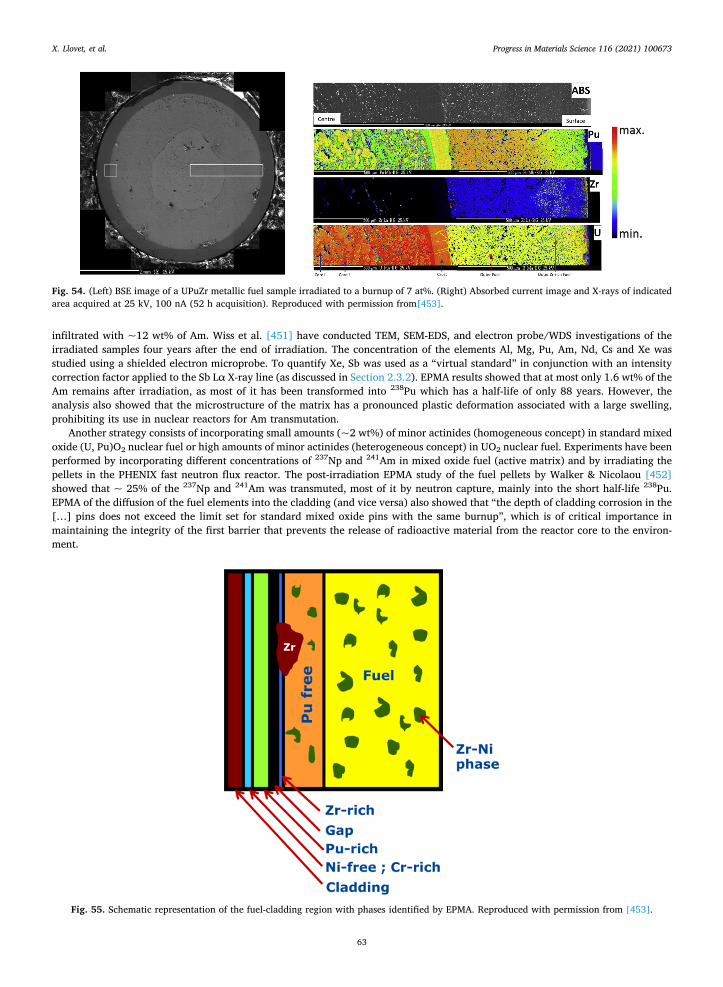
infiltrated with ~12 wt% of Am. Wiss et al. [451] have conducted TEM, SEM-EDS, and electron probe/WDS investigations of the irradiated samples four years after the end of irradiation. The concentration of the elements Al, Mg, Pu, Am, Nd, Cs and Xe was studied using a shielded electron microprobe. To quantify Xe, Sb was used as a “virtual standard” in conjunction with an intensity correction factor applied to the Sb Lα X-ray line (as discussed in Section 2.3.2). EPMA results showed that at most only 1.6 wt% of the Am remains after irradiation, as most of it has been transformed into 238Pu which has a half-life of only 88 years. However, the analysis also showed that the microstructure of the matrix has a pronounced plastic deformation associated with a large swelling, prohibiting its use in nuclear reactors for Am transmutation.
Another strategy consists of incorporating small amounts (~2 wt%) of minor actinides (homogeneous concept) in standard mixed oxide (U, Pu)O2 nuclear fuel or high amounts of minor actinides (heterogeneous concept) in UO2 nuclear fuel. Experiments have been performed by incorporating different concentrations of 237Np and 241Am in mixed oxide fuel (active matrix) and by irradiating the pellets in the PHENIX fast neutron flux reactor. The post-irradiation EPMA study of the fuel pellets by Walker & Nicolaou [452] showed that ~ 25% of the 237Np and 241Am was transmuted, most of it by neutron capture, mainly into the short half-life 238Pu. EPMA of the diffusion of the fuel elements into the cladding (and vice versa) also showed that “the depth of cladding corrosion in the […] pins does not exceed the limit set for standard mixed oxide pins with the same burnup”, which is of critical importance in maintaining the integrity of the first barrier that prevents the release of radioactive material from the reactor core to the environ-ment.
Fig. 54. (Left) BSE image of a UPuZr metallic fuel sample irradiated to a burnup of 7 at%. (Right) Absorbed current image and X-rays of indicated area acquired at 25 kV, 100 nA (52 h acquisition). Reproduced with permission from[453].
Fig. 55. Schematic representation of the fuel-cladding region with phases identified by EPMA. Reproduced with permission from [453].
X. Llovet, et al. Progress in Materials Science 116 (2021) 100673
63
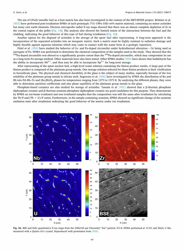
The use of UPuZr metallic fuel as a host matrix has also been investigated in the context of the METAPHIX project. Brémier et al. [453] have performed post-irradiation EPMA of such prototypic 71U-19Pu-10Zr wt% matrix material, containing no minor actinides but many rare earth elements. Electron microprobe radial X-ray maps showed that there was an almost complete depletion of Zr in the central region of the pellet (Fig. 54). The analysis also showed the limited extent of the interaction between the fuel and the cladding, indicating the good behavior of this type of fuel during irradiation (Fig. 55).
Another option for the disposal of actinides is the storage of the spent fuel after reprocessing. A long-term approach is the incorporation of the separated actinides into an inorganic matrix. Such a matrix must be highly resistant to radiation damage and highly durable against aqueous solutions which may come in contact with the waste form in a geologic repository.
Pöml et al. [454] have studied the behavior of Ce- and Pu-doped zirconolite under hydrothermal alteration – Ce being used as surrogate of Pu. EPMA was performed to determine the chemical composition of the samples used in the study. They showed that the 238Pu-doped zirconolite was altered to a significantly greater extent than the 239Pu-doped zirconolite, which may compromise its use as a long-term Pu storage method. Other materials have also been tested. Other EPMA studies [455] have shown that baddeleyite has the ability to incorporate Nb5+, and thus may be able to incorporate Np5+ for long-term storage.
After reprocessing of the spent nuclear fuel, a high-level waste solution containing the fission product results. A large part of the fission product is composed of the platinum group metals. One storage solution selected for these fission products is their vitrification in borosilicate glass. The physical and chemical durability of the glass is the subject of many studies, especially because of the low solubility of the platinum group metals in silicate melt. Sugawara et al. [456] have investigated by EPMA the distribution of Ru and Rh into Pd–Rh–Te and (Ru,Rh)O2 phases for temperature ranging from 1273 to 1573 K. By analyzing the different phases, they were able to determine partition coefficients and also phase equilibria of the platinum group metals in the glass.
Phosphate-based ceramics are also studied for storage of actinides. Tamain et al. [457] showed that a β-thorium phosphate diphosphate ceramic and β-thorium uranium phosphate diphosphate ceramic are good candidates for this purpose. They demonstrate by EPMA on ion-beam irradiated and non-irradiated samples that the composition was still the same after irradiation by calculating the Th/P and (Th + U)/P ratios. Furthermore, in the sample containing uranium, EPMA showed no significant change of the uranium oxidation state after irradiation indicating the good behavior of the matrix under ion irradiation.
Fig. 56. BSE and fully quantitative X-ray maps from the 240x165 μm Chernobyl “hot” particle #2–8. EPMA performed at 15 kV and 20nA; U Mα measured with a Quartz 1011 crystal. Reproduced with permission from [459].
X. Llovet, et al. Progress in Materials Science 116 (2021) 100673
64

3.8.3. Severe accidents Unfortunately, despite the (hopefully) very high levels of safety of the nuclear reactors, several severe accidents have happened
(e.g., Three Mile Island, Chernobyl, and more recently, Fukushima). To understand the chain of events that lead to the accidents, materials extracted from the nuclear accident sites have been studied. As an example, EPMA of “hot” particles of the Chernobyl “lava” (this lava-type material is also known as corium) were conducted by Pöml et al. [456,459]. Quantitative X-ray element maps of elements Nb, Zr, U and O were performed on a U-bearing metallic Zr particle (Fig. 56). Veins of U + Nb were too small to be quantified at 15 kV but the authors reported that their content was at least 55 wt% U and 30 wt% Nb. X-ray maps, as well as EPMA point analysis also correlated with BSE observations and showed that the differences in grey scale contrast correspond with different O content of the Zr matrix. By comparing the oxidation of the particle with other Zr-steam interaction experiments, the authors were able to deduce that the time during which the particle was heated, interacted with the nuclear fuel, and was cooled, occurred faster than 0.3 ms. This supports the idea that the reactor core went supercritical just before the steam explosion and the vessel rupture.
To help improvement for the safety of nuclear reactors, experiments are conducted to study the degradation of irradiated fuel rods in conditions of typical severe accidents. In a series of articles, Bottomley et al. [460] and Bottomley et al. [461] analyzed by EPMA samples coming from the FPT1 experiment in which a UO2 fuel assembly has been partially melted. The complete characterization (X- ray maps, traverses and point analyses) of discs cut from the lower and upper part of the assembly were performed allowing the study of the formed corium itself and its interaction with the Zircaloy cladding for different stages of melting.
Using the virtual standard method, Moy et al. [462] converted experimental X-ray intensities of different X-ray lines (Pt Mα, Au Mα, Pb Mα and Mβ, U Mα and Mβ, and Th Mα and Mβ) into absolute units, at several accelerating voltages ranging from 6 kV to more than 25 kV. These absolute intensities can be used by other laboratories, following the same procedure (Fig. 57), as virtual standards to quantify actinide-bearing materials. The absolute X-ray intensities for these lines, predicted by the Monte Carlo code PENEPMA, were also in very good agreement with the experimental data. The measured X-ray intensity of pure elements varies continuously and smoothly between neighboring elements, i.e., elements with contiguous atomic numbers, as long as the spectro-meter efficiency also varies smoothly. The X-ray intensity of a pure standard can be predicted with a good accuracy by fitting the intensity emitted by the closest neighboring elements. Moy [18] used the Monte Carlo simulation method to quantify uranium in an UO2 sample using the U Mα line, in a ThO2 and a ThF4 sample using the Th Mα line, in a PuO2 sample using the Pu Mα line and in a (U,Pu)O2 sample using the Pu Mβ line. The resulting concentration values were within at least 10% of the expected concentrations.
4. Conclusions
EPMA has continued to be a key characterization tool for materials science and engineering applications since its rapid worldwide introduction in the 1960s. It is a powerful technique to better understand the materials being studied, both natural and synthetic, and is essential for advances in technology, to solve modern day problems (Section 3). With the development of new instrumentation (larger traditional detectors, brighter electron sources and new, innovative detectors; Section 2.12) and an increase of automation and computer control and data processing, it has been possible to generate a large quantity of results quickly easily. However, one should not neglect the importance of understanding the physical principles and experimental procedures (Section 2) behind the easily acquired large data sets, and importantly, the possible limitations, particularly for samples with special geometries (Section 2.5), such as features close to phase boundaries (Section 2.5.2), particles and inclusions (Section 2.5.3), and light elements (Section 2.6) and trace elements (Section 2.8). Additional practical and detailed information is provided in Appendix C.
As reviewers with decades of experience, we wish to point out a few facts and trends, in order to help optimize the usage of EPMA in the materials science and engineering world.
(1) There is an underutilization of EPMA for evaluation of thin film determination. This is most likely due to the limited spread of information about this very useful technique.
(2) There is an underappreciation for the potential errors when only normalized weight percent analytical results are reported in publications (Appendix C.4.1), especially when the quantification was performed using standardless SEM-EDS. SEM-EDS labs doing EPMA would benefit from quality control routines, utilizing standard reference materials as either primary or secondary
Fig. 57. Schematic representing the process to generate virtual EPMA standards for Pb and U, with results within 10% of actual measurements. Reproduced with permission from [462].
X. Llovet, et al. Progress in Materials Science 116 (2021) 100673
65
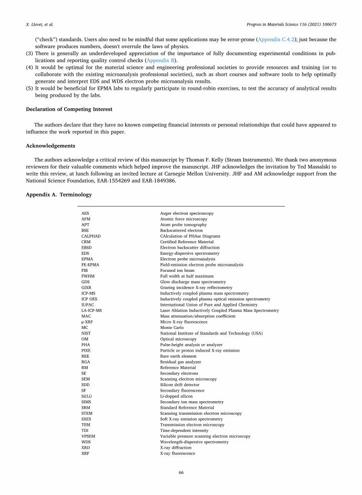
(“check”) standards. Users also need to be mindful that some applications may be error-prone (Appendix C.4.2); just because the software produces numbers, doesn't overrule the laws of physics.
(3) There is generally an underdeveloped appreciation of the importance of fully documenting experimental conditions in pub-lications and reporting quality control checks (Appendix B).
(4) It would be optimal for the material science and engineering professional societies to provide resources and training (or to collaborate with the existing microanalysis professional societies), such as short courses and software tools to help optimally generate and interpret EDS and WDS electron probe microanalysis results.
(5) It would be beneficial for EPMA labs to regularly participate in round-robin exercises, to test the accuracy of analytical results being produced by the labs.
Declaration of Competing Interest
The authors declare that they have no known competing financial interests or personal relationships that could have appeared to influence the work reported in this paper.
Acknowledgements
The authors acknowledge a critical review of this manuscript by Thomas F. Kelly (Steam Instruments). We thank two anonymous reviewers for their valuable comments which helped improve the manuscript. JHF acknowledges the invitation by Ted Massalski to write this review, at lunch following an invited lecture at Carnegie Mellon University. JHF and AM acknowledge support from the National Science Foundation, EAR-1554269 and EAR-1849386.
Appendix A. Terminology
AES Auger electron spectroscopy AFM Atomic force microscopy APT Atom probe tomography BSE Backscattered electron CALPHAD CAlculation of PHAse Diagrams CRM Certified Reference Material EBSD Electron backscatter diffraction EDS Energy-dispersive spectrometry EPMA Electron probe microanalysis FE-EPMA Field-emission electron probe microanalysis FIB Focused ion beam FWHM Full width at half maximum GDS Glow discharge mass spectrometry GIXR Grazing incidence X-ray reflectometry ICP-MS Inductively coupled plasma mass spectrometry ICP OES Inductively coupled plasma optical emission spectrometry IUPAC International Union of Pure and Applied Chemistry LA-ICP-MS Laser Ablation Inductively Coupled Plasma Mass Spectrometry MAC Mass attenuation/absorption coefficient μ-XRF Micro X-ray fluorescence MC Monte Carlo NIST National Institute of Standards and Technology (USA) OM Optical microscopy PHA Pulse-height analysis or analyzer PIXE Particle or proton induced X-ray emission REE Rare earth element RGA Residual gas analyzer RM Reference Material SE Secondary electrons SEM Scanning electron microscopy SDD Silicon drift detector SF Secondary fluorescence Si(Li) Li-dopped silicon SIMS Secondary ion mass spectrometry SRM Standard Reference Material STEM Scanning transmission electron microscopy SXES Soft X-ray emission spectrometry TEM Transmission electron microscopy TDI Time-dependent intensity VPSEM Variable pressure scanning electron microscopy WDS Wavelength-dispersive spectrometry XRD X-ray diffraction XRF X-ray fluorescence
X. Llovet, et al. Progress in Materials Science 116 (2021) 100673
66
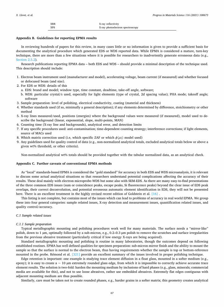
XRR X-ray reflectivity XPS X-ray photoelectron spectroscopy
Appendix B. Guidelines for reporting EPMA results
In reviewing hundreds of papers for this review, in many cases little or no information is given to provide a sufficient basis for documenting the analytical procedure which generated EDS or WDS reported data. While EPMA is considered a mature, turn-key technique, there are more than a few situations where it is possible for researchers to inadvertently generate erroneous data (e.g., Section 2.5.2).
Research publications reporting EPMA data – both EDS and WDS – should provide a minimal description of the technique used. This description should include:
1. Electron beam instrument used (manufacturer and model), accelerating voltage, beam current (if measured) and whether focused or defocused beam (and size).
2. For EDS or WDS: details of this a. EDS: brand and model; window type, time constant, deadtime, take-off angle, software; b. WDS: particular crystal/s used, especially for light elements (type of crystal, 2d spacing value); PHA mode; takeoff angle;
software 3. Sample preparation: level of polishing, electrical conductivity, coating (material and thickness) 4. Whether standards used (if so, minimally a general description); if any elements determined by difference, stoichiometry or other
method 5. X-ray lines measured/used, positions (energies) where the background values were measured (if measured), model used to de-
scribe the background (linear, exponential, slope, multi-points, MAN) 6. Counting time (X-ray line and backgrounds), analytical error, and detection limits 7. If any specific procedures used: anti-contamination; time-dependent counting strategy; interference corrections; if light elements,
source of MACs used 8. Which matrix correction used (i.e, which specific ZAF or which z( ) model used) 9. Any guidelines used for quality control of data (e.g., non-normalized analytical totals, excluded analytical totals below or above a
given wt% threshold, or other criteria).
Non-normalized analytical wt% totals should be provided together with the tabular normalized data, as an analytical check.
Appendix C. Further caveats of conventional EPMA methods
As “local” standards-based EPMA is considered the “gold standard” for accuracy in both EDS and WDS microanalysis, it is relevant to discuss some actual analytical situations so that researchers understand potential complications affecting the accuracy of their results. These deal mainly with electron microprobe-WDS but some also with SEM-EDS. As there are many easy-to-find presentations of the three common EDS issues (sum or coincidence peaks, escape peaks, Si fluorescence peaks) beyond the clear issue of EDS peak overlaps, their correct deconvolution, and potential erroneous automatic element identification in EDS, they will not be presented here. There is an excellent treatment in the highly revised recent edition of Goldstein et al. [16] .
This listing is not complete, but contains most of the issues which can lead to problems of accuracy in real world EPMA. We group these into four general categories: sample related issues, X-ray detection and measurement issues, quantification related issues, and quality control/accuracy.
C.1 Sample related issues
C.1.1 Sample preparation Typical metallographic mounting and polishing procedures work well for many materials. The surface needs a “mirror-like”
polish, down to 1 µm, optimally followed by a sub-micron, e.g., 0.2–0.3 μm polish to remove the scratches and surface irregularities from the previous abrasive treatment (particularly critical if low energy X-rays are being acquired).
Standard metallographic mounting and polishing is routine in many laboratories, though the outcomes depend on following established routines. EPMA has well defined qualities for specimen preparation: sub-micron mirror finish and the ability to mount the sample so that the surface is normal to the electron beam, thus having requirements whether the sample is top or bottom-reference mounted in the probe. Rémond et al. [321] provide an excellent summary of the issues involved in proper polishing technique.
Edge retention is important: one example is studying trace element diffusion in a float glass, mounted in a softer medium (e.g., epoxy); it is easy to create a ~ 10 µm extremely rounded glass edge, from which it is impossible to correctly achieve accurate trace element results. The solution is two-fold: harden the mounting medium by inclusions of hard phases (e.g., glass, minerals; commercial media are available for this), and not to use loose abrasives, rather use embedded abrasives. Extremely flat edges contiguous with adjacent mounting medium are thus possible.
Similarly, care must be taken not to create rounded phases, e.g., harder grains in a softer matrix; this geometry creates analytical
X. Llovet, et al. Progress in Materials Science 116 (2021) 100673
67
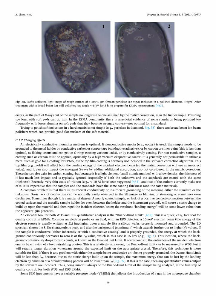
errors, as the path of X-rays out of the sample no longer is the one assumed by the matrix correction, as in the first example. Polishing too long with soft pads can do this. In the EPMA community there is anecdotal evidence of some standards being polished too frequently with loose alumina on soft pads that they become strongly convex—not optimal for a standard.
Trying to polish soft inclusions in a hard matrix is not simple (e.g., periclase in diamond, Fig. 58); there are broad beam ion beam polishers which can provide good flat surfaces of the soft material.
C.1.2 Charging effects An electrically conductive mounting medium is optimal. If nonconductive media (e.g., epoxy) is used, the sample needs to be
grounded to the metal holder by conductive carbon or copper tape (conductive adhesive), or by carbon or silver paint (this is less than optimal, as flaking occurs and can get on O-rings causing vacuum leaks), or by conductively coating. For non-conductive samples, a coating such as carbon must be applied, optimally by a high vacuum evaporative coater. It is generally not permissible to utilize a metal such as gold for a coating for EPMA, as the top film coating is normally not included in the software correction algorithm. This top film (e.g., gold) will affect both the landing energy of the incident electron beam (so the matrix correction will use an incorrect value), and it can also impact the emergent X-rays by adding additional absorption, also not considered in the matrix correction. These factors also exist for carbon coating, but because it is a light element (small atomic number) with a low density, the thickness of it has much less impact and is typically ignored (especially if both the unknown and the standards are coated with the same thickness). Recently, very thin coats of iridium (e.g., < 10 Å) have been suggested [464], and two of the authors currently make use of it. It is imperative that the samples and the standards have the same coating thickness (and the same material).
A common problem is that there is insufficient conductivity or insufficient grounding of the material, either the standard or the unknown. Gross lack of conduction can be normally easily observed in the SE image as blurring or streaking or sometimes even discharges. Sometimes though it is a matter of degree. A poorly coated sample, or lack of a positive contact/connection between the coated surface and the metallic sample holder (or even between the holder and the instrument ground), will cause a static charge to build up upon the material and then repel the incident electron beam; the resultant “landing energy” will be some lower value than the apparent gun potential.
An essential tool for both WDS and EDS quantitative analysis is the “Duane-Hunt Limit” [465]. This is a quick, easy, free tool for quality control in EPMA. Consider an electron probe or an SEM, with an EDS detector; a 15-keV electron beam (the energy of the electron source is usually written as E0) impinging upon a sample like a silicon wafer, properly mounted and grounded. The ED spectrum shows the Si Kα characteristic peak, and also the background (continuum) which extends further out to higher kV values. If the sample is conductive (either inherently or with a conductive coating) and is properly grounded, the energy at which the back-ground continuously decreases to zero is at the E0 value, which in this case is 15 keV (e.g., Fig. 4). This location, where the back-ground continuously drops to zero counts, is known as the Duane-Hunt Limit. It corresponds to the entire loss of the incident electron energy by emission of a bremsstrahlung photon. This is a relatively rare event; the Duane-Hunt limit can be measured by WDS, but it will require longer duration wavescans around the expected limit on the appropriate crystal. Therefore, this technique is more suitable for EDS. If there is any problem with either the sample being conductive or it being properly grounded, the Duane-Hunt Limit will be less than E0, because, due to the static charge built up on the sample, the maximum energy that can be lost by the landing electron by emission of a bremsstrahlung photon will be lower than E0 (Fig. 59). If this is the case, then any quantitative values output by the software are incorrect. Thus, being mindful always of the Duane-Hunt Limit of the sample being analyzed, is the first step of quality control, for both WDS and EDS EPMA.
Some SEM instruments have a variable pressure mode (VPSEM) that allows the introduction of a gas in the microscope chamber
Fig. 58. (Left) Reflected light image of rough surface of a 20x40 μm ferroan periclase (Fe-MgO) inclusion in a polished diamond. (Right) After treatment with a broad beam ion mill polisher; low angle 4–5 kV for 3 h, to prepare for EPMA measurement [463].
X. Llovet, et al. Progress in Materials Science 116 (2021) 100673
68
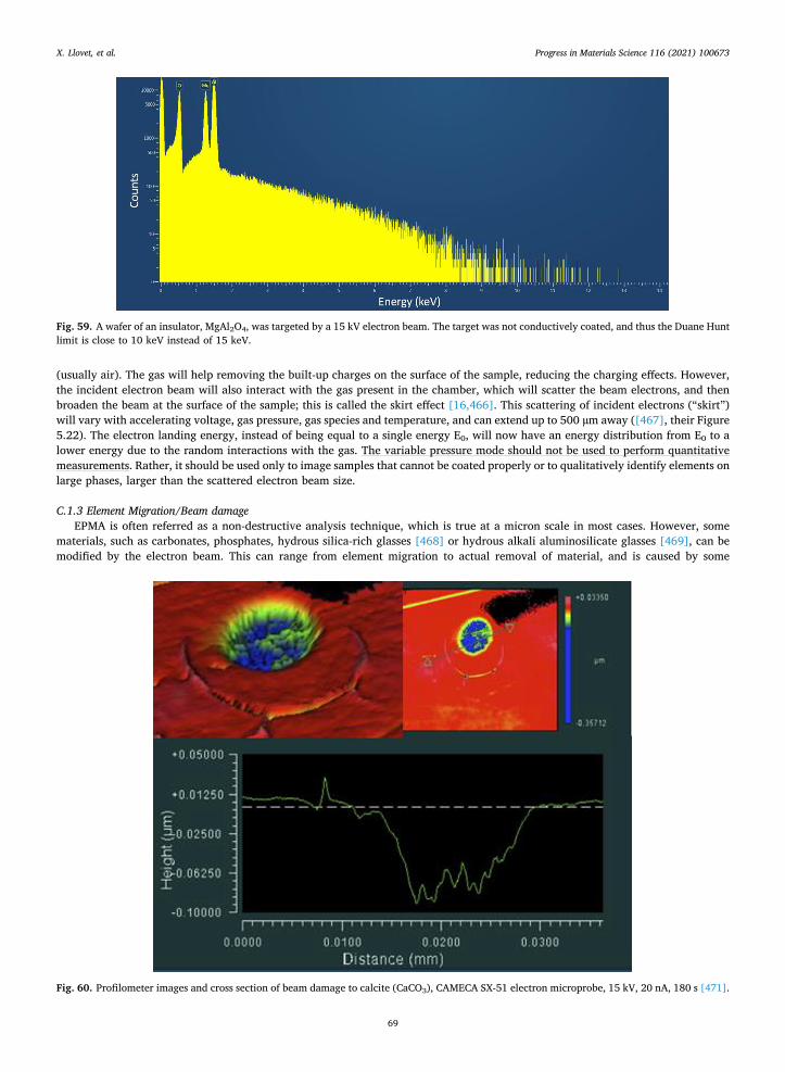
(usually air). The gas will help removing the built-up charges on the surface of the sample, reducing the charging effects. However, the incident electron beam will also interact with the gas present in the chamber, which will scatter the beam electrons, and then broaden the beam at the surface of the sample; this is called the skirt effect [16,466]. This scattering of incident electrons (“skirt”) will vary with accelerating voltage, gas pressure, gas species and temperature, and can extend up to 500 µm away ([467], their Figure 5.22). The electron landing energy, instead of being equal to a single energy E0, will now have an energy distribution from E0 to a lower energy due to the random interactions with the gas. The variable pressure mode should not be used to perform quantitative measurements. Rather, it should be used only to image samples that cannot be coated properly or to qualitatively identify elements on large phases, larger than the scattered electron beam size.
C.1.3 Element Migration/Beam damage EPMA is often referred as a non-destructive analysis technique, which is true at a micron scale in most cases. However, some
materials, such as carbonates, phosphates, hydrous silica-rich glasses [468] or hydrous alkali aluminosilicate glasses [469], can be modified by the electron beam. This can range from element migration to actual removal of material, and is caused by some
Fig. 59. A wafer of an insulator, MgAl2O4, was targeted by a 15 kV electron beam. The target was not conductively coated, and thus the Duane Hunt limit is close to 10 keV instead of 15 keV.
Fig. 60. Profilometer images and cross section of beam damage to calcite (CaCO3), CAMECA SX-51 electron microprobe, 15 kV, 20 nA, 180 s [471].
X. Llovet, et al. Progress in Materials Science 116 (2021) 100673
69
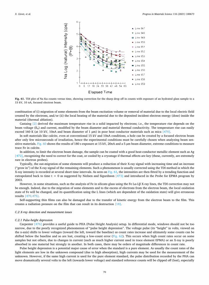
combination of (i) migration of some elements from the beam excitation volume or removal of material due to the local electric field created by the electrons, and/or (ii) the local heating of the material due to the deposited incident electron energy (dose) inside the material (thermal ablation).
Castaing [2] derived the maximum temperature rise in a solid impacted by electrons; i.e., the temperature rise depends on the beam voltage (E0) and current, modified by the beam diameter and material thermal conductivity. The temperature rise can easily exceed 160 K (at 10 kV, 10nA and beam diameter of 1 µm) in poor heat conductor materials such as mica [470].
In soft materials like calcite, even at conventional 15 kV and 10nA conditions, a hole can be created by a focused electron beam after only few microseconds of irradiation, hence the experimental conditions must be carefully chosen when analyzing beam sen-sitive materials. Fig. 60 shows the results of 180 s exposure at 15 kV, 20nA and a 5 µm beam diameter, extreme conditions to measure trace Fe in calcite.
In addition, to limit the electron beam damage, the sample can be coated with a good heat-conductor metallic element such as Ag [472], recognizing the need to correct for the coat, or cooled by a cryostage if thermal effects are key (these, currently, are extremely rare in electron probes).
Typically, the out-migration of some elements will produce a reduction of their X-ray signal with increasing time and an increase (“grow in”) of the X-ray signal of the remaining elements. Such a phenomenon is usually corrected using the TDI method in which the X-ray intensity is recorded at several short time intervals. As seen on Fig. 61, the intensities are then fitted by a trending function and extrapolated back to time t = 0 as suggested by Nielsen and Sigurdsson [473] and introduced in the Probe for EPMA program by 2003.
However, in some situations, such as the analysis of Fe in silicate-glass using the Fe Lα-Lβ X-ray lines, the TDI correction may not be enough. Indeed, due to the migration of some elements and to the excess of electrons from the electron beam, the local oxidation state of Fe will be changed, and its quantification using the L lines (which are dependent of the oxidation state) will give erroneous results [470,475].
Self-supporting thin films can also be damaged due to the transfer of kinetic energy from the electron beam to the film. This creates a radiation pressure on the film that can result in its destruction [18].
C.2 X-ray detection and measurement issues
C.2.1 Pulse-height depression Carpenter [476] provides a useful guide to PHA (Pulse Height Analysis) setup. In differential mode, windows should not be too
narrow, due to the poorly recognized phenomenon of “pulse height depression”. The voltage pulse (its “height” in volts, viewed on the x-axis) shifts to lower voltages (toward the left, toward the baseline) as count rates increase and ultimately some counts can be shifted below the baseline and so are lost, creating a low-count error (Fig. 62). This occurs when high count rates occur on some samples but not others, due to changes in current (such as much higher current used in trace element EPMA) or an X-ray is poorly absorbed in one material but strongly in another. In both cases, there may be orders of magnitude differences in count rate.
Pulse height depression is a potential major cause of error when the standard is a pure element. As usually the count rates of the light elements are low in the unknown compound (due to high absorption), high currents may be used for the measurement of the unknown. However, if the same high current is used for the pure element standard, the pulse distribution recorded by the PHA can move dramatically several volts to the left (towards lower voltage) and standard reference counts will be clipped off (lost), especially
Fig. 61. TDI plot of Na Kα counts versus time, showing correction for the sharp drop off in counts with exposure of an hydrated glass sample to a 15 kV, 10 nA, focused electron beam.
X. Llovet, et al. Progress in Materials Science 116 (2021) 100673
70
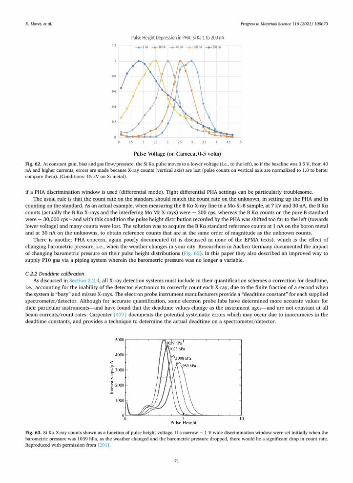
if a PHA discrimination window is used (differential mode). Tight differential PHA settings can be particularly troublesome. The usual rule is that the count rate on the standard should match the count rate on the unknown, in setting up the PHA and in
counting on the standard. As an actual example, when measuring the B Kα X-ray line in a Mo-Si-B sample, at 7 kV and 30 nA, the B Kα counts (actually the B Kα X-rays and the interfering Mo Mξ X-rays) were ~ 300 cps, whereas the B Kα counts on the pure B standard were ~ 30,000 cps – and with this condition the pulse height distribution recorded by the PHA was shifted too far to the left (towards lower voltage) and many counts were lost. The solution was to acquire the B Kα standard reference counts at 1 nA on the boron metal and at 30 nA on the unknowns, to obtain reference counts that are at the same order of magnitude as the unknown counts.
There is another PHA concern, again poorly documented (it is discussed in none of the EPMA texts), which is the effect of changing barometric pressure, i.e., when the weather changes in your city. Researchers in Aachen Germany documented the impact of changing barometric pressure on their pulse height distributions (Fig. 63). In this paper they also described an improved way to supply P10 gas via a piping system wherein the barometric pressure was no longer a variable.
C.2.2 Deadtime calibration As discussed in Section 2.2.4, all X-ray detection systems must include in their quantification schemes a correction for deadtime,
i.e., accounting for the inability of the detector electronics to correctly count each X-ray, due to the finite fraction of a second when the system is “busy” and misses X-rays. The electron probe instrument manufacturers provide a “deadtime constant” for each supplied spectrometer/detector. Although for accurate quantification, some electron probe labs have determined more accurate values for their particular instruments—and have found that the deadtime values change as the instrument ages—and are not constant at all beam currents/count rates. Carpenter [477] documents the potential systematic errors which may occur due to inaccuracies in the deadtime constants, and provides a technique to determine the actual deadtime on a spectrometer/detector.
Fig. 62. At constant gain, bias and gas flow/pressure, the Si Kα pulse moves to a lower voltage (i.e., to the left), so if the baseline was 0.5 V, from 40 nA and higher currents, errors are made because X-ray counts (vertical axis) are lost (pulse counts on vertical axis are normalized to 1.0 to better compare them). (Conditions: 15 kV on Si metal).
Fig. 63. Si Kα X-ray counts shown as a function of pulse height voltage. If a narrow ~ 1 V wide discrimination window were set initially when the barometric pressure was 1039 hPa, as the weather changed and the barometric pressure dropped, there would be a significant drop in count rate. Reproduced with permission from [291].
X. Llovet, et al. Progress in Materials Science 116 (2021) 100673
71
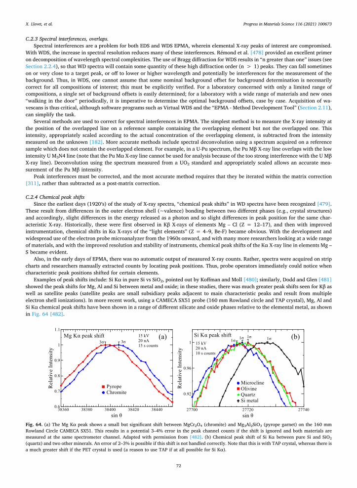
C.2.3 Spectral interferences, overlaps. Spectral interferences are a problem for both EDS and WDS EPMA, wherein elemental X-ray peaks of interest are compromised.
With WDS, the increase in spectral resolution reduces many of these interferences. Rémond et al. [478] provided an excellent primer on decomposition of wavelength spectral complexities. The use of Bragg diffraction for WDS results in “n greater than one” issues (see Section 2.2.4), so that WD spectra will contain some quantity of these high diffraction order (n > 1) peaks. They can fall sometimes on or very close to a target peak, or off to lower or higher wavelength and potentially be interferences for the measurement of the background. Thus, in WDS, one cannot assume that some nominal background offset for background determination is necessarily correct for all compositions of interest; this must be explicitly verified. For a laboratory concerned with only a limited range of compositions, a single set of background offsets is easily determined; for a laboratory with a wide range of materials and new ones “walking in the door” periodically, it is imperative to determine the optimal background offsets, case by case. Acquisition of wa-vescans is thus critical, although software programs such as Virtual WDS and the “EPMA - Method Development Tool” (Section 2.11), can simplify the task.
Several methods are used to correct for spectral interferences in EPMA. The simplest method is to measure the X-ray intensity at the position of the overlapped line on a reference sample containing the overlapping element but not the overlapped one. This intensity, appropriately scaled according to the actual concentration of the overlapping element, is subtracted from the intensity measured on the unknown [182]. More accurate methods include spectral deconvolution using a spectrum acquired on a reference sample which does not contain the overlapped element. For example, in a U-Pu spectrum, the Pu Mβ X-ray line overlaps with the low intensity U M3N4 line (note that the Pu Mα X-ray line cannot be used for analysis because of the too strong interference with the U Mβ X-ray line). Deconvolution using the spectrum measured from a UO2 standard and appropriately scaled allows an accurate mea-surement of the Pu Mβ intensity.
Peak interferences must be corrected, and the most accurate method requires that they be iterated within the matrix correction [311], rather than subtracted as a post-matrix correction.
C.2.4 Chemical peak shifts Since the earliest days (1920′s) of the study of X-ray spectra, “chemical peak shifts” in WD spectra have been recognized [479].
These result from differences in the outer electron shell (~valence) bonding between two different phases (e.g., crystal structures) and accordingly, slight differences in the energy released as a photon and so slight differences in peak position for the same char-acteristic X-ray. Historically, these were first observed in Kβ X-rays of elements Mg – Cl (Z = 12–17), and then with improved instrumentation, chemical shifts in Kα X-rays of the “light elements” (Z = 4–9, Be-F) became obvious. With the development and widespread use of the electron probe microanalyzer from the 1960s onward, and with many more researchers looking at a wide range of materials, and with the improved resolution and stability of instruments, chemical peak shifts of the Kα X-ray line in elements Mg – S became evident.
Also, in the early days of EPMA, there was no automatic output of measured X-ray counts. Rather, spectra were acquired on strip charts and researchers manually extracted counts by locating peak positions. Thus, probe operators immediately could notice when characteristic peak positions shifted for certain elements.
Examples of peak shifts include: Si Kα in pure Si vs SiO2, pointed out by Koffman and Moll [480]; similarly, Dodd and Glen [481] showed the peak shifts for Mg, Al and Si between metal and oxide; in these studies, there was much greater peak shifts seen for Kβ as well as satellite peaks (satellite peaks are small subsidiary peaks adjacent to main characteristic peaks and result from multiple electron shell ionizations). In more recent work, using a CAMECA SX51 probe (160 mm Rowland circle and TAP crystal), Mg, Al and Si Kα chemical peak shifts have been shown in a range of different silicate and oxide phases relative to the elemental metal, as shown in Fig. 64 [482].
Fig. 64. (a) The Mg Kα peak shows a small but significant shift between MgCr2O4 (chromite) and Mg3Al2SiO3 (pyrope garnet) on the 160 mm Rowland Circle CAMECA SX51. This results in a potential 3–4% error in the peak channel counts if the shift is ignored and both materials are measured at the same spectrometer channel. Adapted with permission from [482]. (b) Chemical peak shift of Si Kα between pure Si and SiO2
(quartz) and two other minerals. An error of 2–3% is possible if this shift is not handled correctly. Note that this is with TAP crystal, whereas there is a much greater shift if the PET crystal is used (a reason to use TAP if at all possible for Si Kα).
X. Llovet, et al. Progress in Materials Science 116 (2021) 100673
72
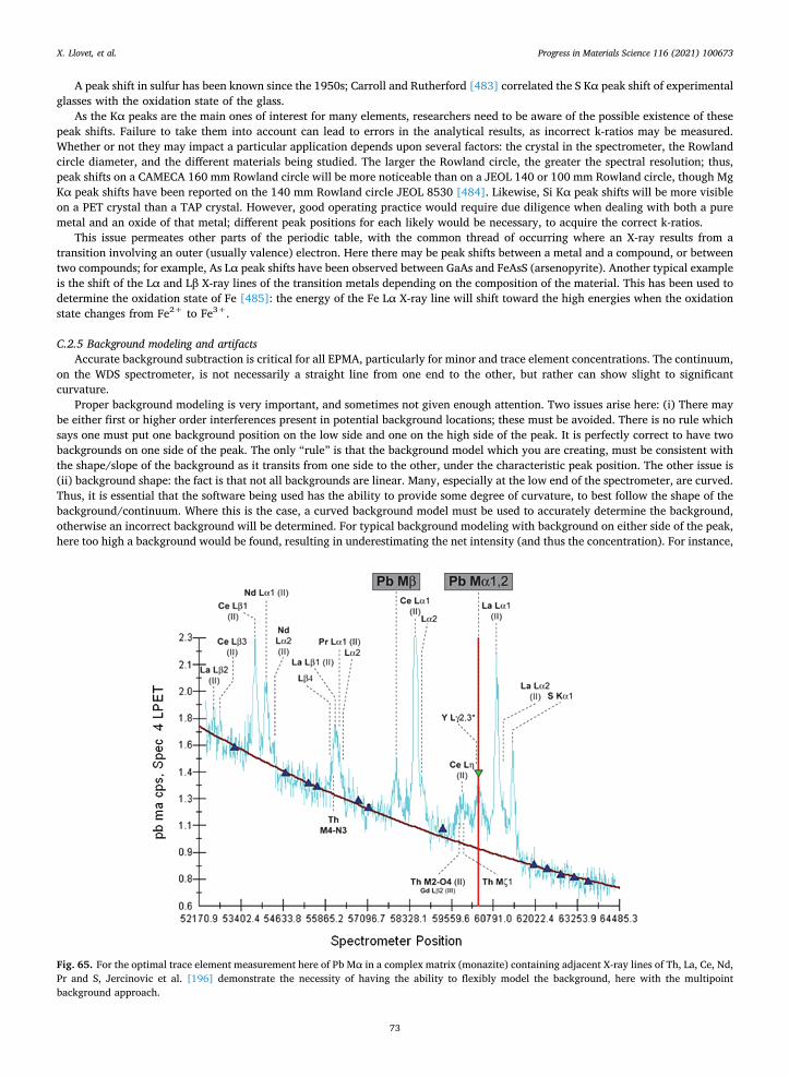
A peak shift in sulfur has been known since the 1950s; Carroll and Rutherford [483] correlated the S Kα peak shift of experimental glasses with the oxidation state of the glass.
As the Kα peaks are the main ones of interest for many elements, researchers need to be aware of the possible existence of these peak shifts. Failure to take them into account can lead to errors in the analytical results, as incorrect k-ratios may be measured. Whether or not they may impact a particular application depends upon several factors: the crystal in the spectrometer, the Rowland circle diameter, and the different materials being studied. The larger the Rowland circle, the greater the spectral resolution; thus, peak shifts on a CAMECA 160 mm Rowland circle will be more noticeable than on a JEOL 140 or 100 mm Rowland circle, though Mg Kα peak shifts have been reported on the 140 mm Rowland circle JEOL 8530 [484]. Likewise, Si Kα peak shifts will be more visible on a PET crystal than a TAP crystal. However, good operating practice would require due diligence when dealing with both a pure metal and an oxide of that metal; different peak positions for each likely would be necessary, to acquire the correct k-ratios.
This issue permeates other parts of the periodic table, with the common thread of occurring where an X-ray results from a transition involving an outer (usually valence) electron. Here there may be peak shifts between a metal and a compound, or between two compounds; for example, As Lα peak shifts have been observed between GaAs and FeAsS (arsenopyrite). Another typical example is the shift of the Lα and Lβ X-ray lines of the transition metals depending on the composition of the material. This has been used to determine the oxidation state of Fe [485]: the energy of the Fe Lα X-ray line will shift toward the high energies when the oxidation state changes from Fe2+ to Fe3+.
C.2.5 Background modeling and artifacts Accurate background subtraction is critical for all EPMA, particularly for minor and trace element concentrations. The continuum,
on the WDS spectrometer, is not necessarily a straight line from one end to the other, but rather can show slight to significant curvature.
Proper background modeling is very important, and sometimes not given enough attention. Two issues arise here: (i) There may be either first or higher order interferences present in potential background locations; these must be avoided. There is no rule which says one must put one background position on the low side and one on the high side of the peak. It is perfectly correct to have two backgrounds on one side of the peak. The only “rule” is that the background model which you are creating, must be consistent with the shape/slope of the background as it transits from one side to the other, under the characteristic peak position. The other issue is (ii) background shape: the fact is that not all backgrounds are linear. Many, especially at the low end of the spectrometer, are curved. Thus, it is essential that the software being used has the ability to provide some degree of curvature, to best follow the shape of the background/continuum. Where this is the case, a curved background model must be used to accurately determine the background, otherwise an incorrect background will be determined. For typical background modeling with background on either side of the peak, here too high a background would be found, resulting in underestimating the net intensity (and thus the concentration). For instance,
Fig. 65. For the optimal trace element measurement here of Pb Mα in a complex matrix (monazite) containing adjacent X-ray lines of Th, La, Ce, Nd, Pr and S, Jercinovic et al. [196] demonstrate the necessity of having the ability to flexibly model the background, here with the multipoint background approach.
X. Llovet, et al. Progress in Materials Science 116 (2021) 100673
73
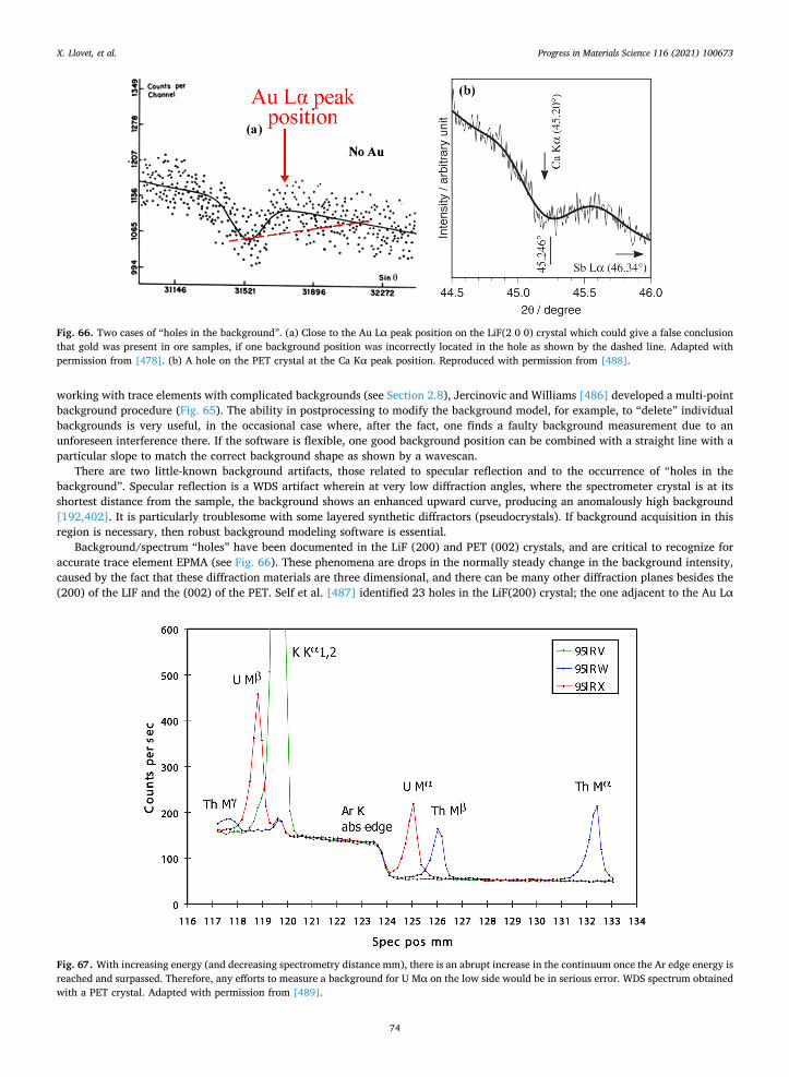
working with trace elements with complicated backgrounds (see Section 2.8), Jercinovic and Williams [486] developed a multi-point background procedure (Fig. 65). The ability in postprocessing to modify the background model, for example, to “delete” individual backgrounds is very useful, in the occasional case where, after the fact, one finds a faulty background measurement due to an unforeseen interference there. If the software is flexible, one good background position can be combined with a straight line with a particular slope to match the correct background shape as shown by a wavescan.
There are two little-known background artifacts, those related to specular reflection and to the occurrence of “holes in the background”. Specular reflection is a WDS artifact wherein at very low diffraction angles, where the spectrometer crystal is at its shortest distance from the sample, the background shows an enhanced upward curve, producing an anomalously high background [192,402]. It is particularly troublesome with some layered synthetic diffractors (pseudocrystals). If background acquisition in this region is necessary, then robust background modeling software is essential.
Background/spectrum “holes” have been documented in the LiF (200) and PET (002) crystals, and are critical to recognize for accurate trace element EPMA (see Fig. 66). These phenomena are drops in the normally steady change in the background intensity, caused by the fact that these diffraction materials are three dimensional, and there can be many other diffraction planes besides the (200) of the LIF and the (002) of the PET. Self et al. [487] identified 23 holes in the LiF(200) crystal; the one adjacent to the Au Lα
Fig. 66. Two cases of “holes in the background”. (a) Close to the Au Lα peak position on the LiF(2 0 0) crystal which could give a false conclusion that gold was present in ore samples, if one background position was incorrectly located in the hole as shown by the dashed line. Adapted with permission from [478]. (b) A hole on the PET crystal at the Ca Kα peak position. Reproduced with permission from [488].
Fig. 67. With increasing energy (and decreasing spectrometry distance mm), there is an abrupt increase in the continuum once the Ar edge energy is reached and surpassed. Therefore, any efforts to measure a background for U Mα on the low side would be in serious error. WDS spectrum obtained with a PET crystal. Adapted with permission from [489].
X. Llovet, et al. Progress in Materials Science 116 (2021) 100673
74
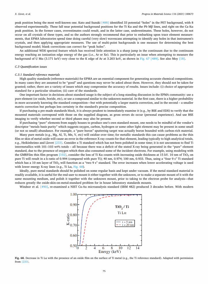
peak position being the most well-known one. Kato and Suzuki [488] identified 33 potential “holes” in the PET background, with 8 observed experimentally. These fall near potential background positions for the Ti Kα and the Pb Mβ lines, and right on the Ca Kα peak position. In the former cases, overestimates could result, and in the latter case, underestimates. These holes, however, do not occur on all crystals of these types, and so the authors strongly recommend that prior to embarking upon trace element measure-ments, that EPMA laboratories spend time doing careful (very slow) wavescans attempting to identify any holes in that instrument's crystals, and then applying appropriate measures. The use of multi-point backgrounds is one measure for determining the best background model; blank corrections can correct for “peak holes”.
An additional WDS spectral feature which has received little attention is a sharp jump in the continuum due to the continuum energy reaching an ionization edge energy of the gas (i.e., Ar or Xe). This is particularly an issue when attempting to measure the background of U Mα (3.171 keV) very close to the K edge of Ar at 3.203 keV, as shown in Fig. 67 [489]. See also Moy [18].
C.3 Quantification issues
C.3.1 Standard reference materials High quality standards (reference materials) for EPMA are an essential component for generating accurate chemical compositions.
In many cases they are assumed to be “good” and questions may never be asked about them. However, they should not be taken for granted; rather, there are a variety of issues which may compromise the accuracy of results. Issues include: (i) choice of appropriate standard for a particular situation; (ii) care of the standards.
One important factor in decisions about standard usage is the subject of a long-standing discussion in the EPMA community: use a pure element (or oxide, boride, etc), or use a compound similar to the unknown material. In the first case, there is a higher probability in more accurately knowing the standard composition—but with potentially a larger matrix correction, and in the second – a smaller matrix correction but perhaps less certainty in the standard's precise composition.
If purchasing a pre-made standards block, it is always prudent to immediately examine it (e.g., by BSE and EDS) to verify that the mounted materials correspond with those on the supplied diagram, as gross errors do occur (personal experience). And use BSE imaging to verify whether second or third phases may also be present.
If purchasing “pure” elements from supply houses to produce one’s own standard mount, one needs to be mindful of the vendor’s descriptor “metals basis purity” which suggests oxygen, carbon, hydrogen or some other light element may be present in some small (or not so small) abundance. For example, a “pure boron” sputtering target was actually boron bounded with carbon-rich material.
Many pure metals (e.g., Mg, Al, Ti, Mn, V, etc) will oxidize over time; for metallic standards this can cause problems as the thin film or skin of metal oxide will cause an error in the reference X-ray counts for that element, leading typically to high analytical totals, e.g., Heikinheimo and Llovet [233]. Consider a Ti standard which has not been polished in some time; it is not uncommon to find Ti intermetallics with 101–103 wt% totals – all because there was a deficit of the stated X-ray being generated in the “pure” element standard, due to the presence of oxygen which then also consumed some of the incident electrons. For example, using modeling with the GMRFilm thin film program [102], consider the loss of Ti Kα counts with increasing oxide thickness at 15 kV. 10 nm of TiO2 on pure Ti will result in a k-ratio of 0.994 (compared with pure Ti); 40 nm, 0.974; 100 nm, 0.933. Thus, using a “four 9 s” Ti standard which has a 10 nm layer of TiO2 will function as a “two 9 s” standard. The error increases when lower accelerating voltage is used with lower energy X-ray lines (e.g., Ti Lα, Fig. 68).
Ideally, pure metal standards should be polished on some regular basis and kept under vacuum. If the metal standard material is readily available, it is useful for the end-user to mount it either together with the unknown, or to make a separate mount of it with the same mounting medium, and polish it together with the unknown mount, prior to taking to the electron probe for analysis—that reduces greatly the oxide-skin-on-metal-standard problem for in house laboratory standards mounts.
Windsor et al. [490], re-examined a NIST Cu-Au microanalysis standard (SRM 482) produced 3 decades before. With modern
Fig. 68. Decrease in Ti Lα with the presence of an oxide film on the surface of Ti metal (e.g., the Ti reference standard). Adapted with permission from [233].
X. Llovet, et al. Progress in Materials Science 116 (2021) 100673
75
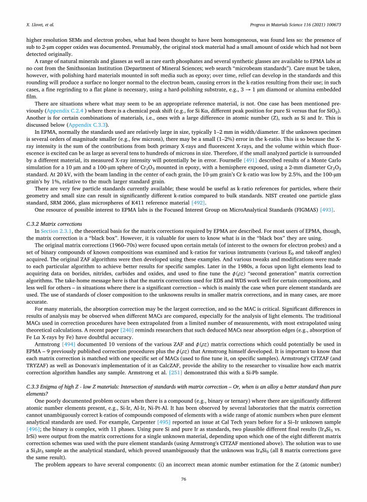
higher resolution SEMs and electron probes, what had been thought to have been homogeneous, was found less so: the presence of sub to 2-µm copper oxides was documented. Presumably, the original stock material had a small amount of oxide which had not been detected originally.
A range of natural minerals and glasses as well as rare earth phosphates and several synthetic glasses are available to EPMA labs at no cost from the Smithsonian Institution (Department of Mineral Sciences; web search “microbeam standards”). Care must be taken, however, with polishing hard materials mounted in soft media such as epoxy; over time, relief can develop in the standards and this rounding will produce a surface no longer normal to the electron beam, causing errors in the k-ratios resulting from their use; in such cases, a fine regrinding to a flat plane is necessary, using a hard-polishing substrate, e.g., 3 → 1 µm diamond or alumina embedded film.
There are situations where what may seem to be an appropriate reference material, is not. One case has been mentioned pre-viously (Appendix C.2.4 ) where there is a chemical peak shift (e.g., for Si Kα, different peak position for pure Si versus that for SiO2). Another is for certain combinations of materials, i.e., ones with a large difference in atomic number (Z), such as Si and Ir. This is discussed below (Appendix C.3.3).
In EPMA, normally the standards used are relatively large in size, typically 1–2 mm in width/diameter. If the unknown specimen is several orders of magnitude smaller (e.g., few microns), there may be a small (1–2%) error in the k-ratio. This is so because the X- ray intensity is the sum of the contributions from both primary X-rays and fluorescent X-rays, and the volume within which fluor-escence is excited can be as large as several tens to hundreds of microns in size. Therefore, if the small analyzed particle is surrounded by a different material, its measured X-ray intensity will potentially be in error. Fournelle [491] described results of a Monte Carlo simulation for a 10 µm and a 100-µm sphere of Cr2O3 mounted in epoxy, with a hemisphere exposed, using a 2-mm diameter Cr2O3
standard. At 20 kV, with the beam landing in the center of each grain, the 10-µm grain’s Cr k-ratio was low by 2.5%, and the 100-µm grain’s by 1%, relative to the much larger standard grain.
There are very few particle standards currently available; these would be useful as k-ratio references for particles, where their geometry and small size can result in significantly different k-ratios compared to bulk standards. NIST created one particle glass standard, SRM 2066, glass microspheres of K411 reference material [492].
One resource of possible interest to EPMA labs is the Focused Interest Group on MicroAnalytical Standards (FIGMAS) [493].
C.3.2 Matrix corrections In Section 2.3.1, the theoretical basis for the matrix corrections required by EPMA are described. For most users of EPMA, though,
the matrix correction is a “black box”. However, it is valuable for users to know what is in the “black box” they are using. The original matrix corrections (1960–70s) were focused upon certain metals (of interest to the owners for electron probes) and a
set of binary compounds of known compositions was examined and k-ratios for various instruments (various E0 and takeoff angles) acquired. The original ZAF algorithms were then developed using these examples. And various tweaks and modifications were made to each particular algorithm to achieve better results for specific samples. Later in the 1980s, a focus upon light elements lead to acquiring data on borides, nitrides, carbides and oxides, and used to fine tune the z( ) “second generation” matrix correction algorithms. The take-home message here is that the matrix corrections used for EDS and WDS work well for certain compositions, and less well for others – in situations where there is a significant correction – which is mainly the case when pure element standards are used. The use of standards of closer composition to the unknowns results in smaller matrix corrections, and in many cases, are more accurate.
For many materials, the absorption correction may be the largest correction, and so the MAC is critical. Significant differences in results of analysis may be observed when different MACs are compared, especially for the analysis of light elements. The traditional MACs used in correction procedures have been extrapolated from a limited number of measurements, with most extrapolated using theoretical calculations. A recent paper [240] reminds researchers that such deduced MACs near absorption edges (e.g., absorption of Fe Lα X-rays by Fe) have doubtful accuracy.
Armstrong [494] documented 10 versions of the various ZAF and z( ) matrix corrections which could potentially be used in EPMA – 9 previously published correction procedures plus the z( ) that Armstrong himself developed. It is important to know that each matrix correction is matched with one specific set of MACs (used to fine tune it, on specific samples). Armstrong's CITZAF (and TRYZAF) as well as Donovan's implementation of it as CalcZAF, provide the ability to the researcher to visualize how each matrix correction algorithm handles any sample. Armstrong et al. [251] demonstrated this with a Si-Pb sample.
C.3.3 Enigma of high Z - low Z materials: Intersection of standards with matrix correction – Or, when is an alloy a better standard than pure elements?
One poorly documented problem occurs when there is a compound (e.g., binary or ternary) where there are significantly different atomic number elements present, e.g., Si-Ir, Al-Ir, Ni-Pt-Al. It has been observed by several laboratories that the matrix correction cannot unambiguously correct k-ratios of compounds composed of elements with a wide range of atomic numbers when pure element analytical standards are used. For example, Carpenter [495] reported an issue at Cal Tech years before for a Si–Ir unknown sample [496]; the binary is complex, with 11 phases. Using pure Si and pure Ir as standards, two plausible different final results (Ir4Si5 vs. IrSi) were output from the matrix corrections for a single unknown material, depending upon which one of the eight different matrix correction schemes was used with the pure element standards (using Armstrong's CITZAF mentioned above). The solution was to use a Si3Ir5 sample as the analytical standard, which proved unambiguously that the unknown was Ir4Si5 (all 8 matrix corrections gave the same result).
The problem appears to have several components: (i) an incorrect mean atomic number estimation for the Z (atomic number)
X. Llovet, et al. Progress in Materials Science 116 (2021) 100673
76
correction of phases with disparate Z values, (ii) failure to include continuum fluorescence which can be a problem for high atomic number standards (e.g., Ir, Pt), and (iii) to a possibly smaller extent, choice of the best mass absorption coefficients. Potentially there is also (iv) the possibility for peak shifts in low-energy X-ray lines (e.g., Si Kα, Al Kα, Mg Kα, etc.), though this is easy to determine and correct.
In a study of Ni-Pt-Al [497], the effect of different matrix corrections on the X-ray measurements was shown when ten different matrix correction algorithms and associated factors were used to correct the same k-ratio for alloy Ni–24.2Al–31.1Pt for X-ray intensities measured using standards-based electron microprobe-WDS. In addition to the wide range of possible values for each element in this unknown phase, the analytical totals outside of the acceptable range of 99–101 wt% suggested a significant in-accuracy in the results. Also, different values are calculated when Pt Lα is used rather than Pt Mα. Based upon the experience at Cal Tech cited above, the researchers selected an intermediate alloy as the standard because there is only one homogenized phase in the microstructure. This sample was sent out for independent chemical analysis, to verify the composition. It was then used as the EPMA analytical standard. When using this approach, there is much less extrapolating from extreme end member elemental compositions, and the matrix corrections converged upon a tighter compositional range. Using this experimental single phase as the standard, significantly different results were obtained for the alloy Ni–24.2Al–31.1Pt compared to those determined originally with pure element standards.
C.4 Final results
C.4.1 Accuracy criteria For confidence in the accuracy of results, standards-based EPMA, for both WDS and EDS – explicitly using a "local" reference
material to acquire X-ray counts to generate the required k-ratio – use the simple test: does the analytical mass (weight) percent total fall in a close range around 100 wt% (without normalization to 100)? Optimally a “perfect” analytical total should fall between 99 and 100.5 wt% (more on the low side as there could be minor/trace elements unmeasured), although in the real world a wider leeway is considered acceptable. There is a second quality control criterion, which is applicable for some materials where the elements are known to exist in some well-defined stoichiometric ratio. However, this may be complicated where there can exist a small but real range of solubility in a so-called line compound. There can be a third criterion of charge balance for a covalent bonded material.
There can be a quality control issue, as this review's authors have observed in practice, when EPMA users “only” look at the normalized atomic percent values in the electron probe output. The issue is, if the analytical total is far from 100 wt%, that is an immediate red flag that there are problems with the analysis, e.g., an unanalyzed element in the unknown (low total), a standard with an oxide coat (high total), the unknown having an oxide or other coat (low total), or secondary fluorescence from adjacent phases (high total). That red flag indicates that the normalized atomic values cannot be assumed to be correct. For that reason, the non- normalized weight percent total should always be consulted before the normalized atomic values are accepted, and optimal op-erational reporting would always include analytical (wt%) totals.
C.4.2 Improper applications There are occasions when users of WDS or EDS attempt to use the instrument and analytical process improperly. Here we list three
examples which we have seen in our day-to-day laboratory experiences:
1. “I only am interested in one element in this sample so please don’t measure anything else”: The material obviously has more than one element, and so the X-ray intensity measured for the “target” element is modified by the matrix. And so, ALL elements present in the sample MUST be measured (or at least accounted for), in order to determine the correct concentration of the target element.
2. A version of this is the belief that one can measure by WDS or EDS a thin film composition atop a substrate (where there are no elements in common) “by ignoring the substrate elements and renormalizing the film elements”. Again, this can lead to errors, as the electron beam penetrates through the film and so “sees” the film for only a fraction of the total depth which the electrons travel, and thus those X-rays are not generated at all like the way they are within the reference material (a bulk material). Thus, the k-ratios for the film elements are "incorrect" (this is not a bulk sample) even before they go into the matrix correction. Added to this is the possibility that X-rays in the substrate may cause secondary fluorescence in the film, generating further error. There is a correct way to determine thin film compositions by EDS and WDS, described in Section 3.4.
3. Defocused-beam analysis: There are occasions where EPMA is utilized in an attempt to achieve an area or bulk analysis. Recall that the interaction volume of 15–20 kV incident electron beams is on the order of 1–2 µm, dependent upon the target compo-sition and density. However, sometimes requests come to a probe laboratory to determine the chemical composition of a small, heterogeneous/multiple phase region within a sample. As the electron beam in spot mode can be defocused, or it can be set in a rectangular scan mode, there can be belief that these defocused/scan modes can collect X-rays from a large (up to 50–100 µm wide) area, yielding a correct average chemical composition. However, this application of EPMA is prone to errors, as it violates a key principle for the correction procedure (X-rays → k-ratio → matrix correction → result for each discrete analytical volume) which is that the interaction volume is homogenous, so that a unique correction be determined. If the beam is generating X-rays from more than one chemical composition, then the matrix correction will average the correction factors, creating errors. As in many situations the absorption correction can be the largest correction, overscanning in many cases generates symptomatically high totals. This has been discussed by Carpenter et al. [498]. Barkman et al. [204] demonstrate the proper procedure, acquiring quantitative X-ray maps, which can be then processed to generate correct small area bulk compositions.
X. Llovet, et al. Progress in Materials Science 116 (2021) 100673
77
References
[1] ISO 23833:2013. Microbeam analysis — Electron probe microanalysis (EPMA) — Vocabulary 2013. [2] Castaing R. Application of electron probes to local chemical and crystallographic analysis (Ph.D. Thesis). University of Paris; 1951.http://www.
microbeamanalysis.org/history/Castaing-Thesis-clearscan.pdf. Thesis translated by P. Duwez, D.B. Wittry (1955). [3] Castaing R. Electron Probe Microanalysis. Electronic and Electron Phys. 1960:317–86. https://doi.org/10.1016/S0065-2539(08)60212-7. [4] Newbury DE. Castaing’s electron microprobe and its impact on materials science. Microsc Microanal 2001:178–92. https://doi.org/10.1007/s100050010082. [5] Castaing R, Guinier A. Application des sondes électroniques à l’analyse métallographique. Proceeding 1st Int. Conf. Electron Microsc., Delft: 1949, p. 60–3. [6] Castaing R. Microanalysis by means of an electron probe: principle and corrections and applications of the electron probe microanalyzer. Proc. Electron Phys.,
NBS Circular 1954;527, NS, 1951:305–9. [7] Lowe BG, Sareen RA. Semiconductor X-ray detectors. CRC Press; 2013. https://doi.org/10.1201/b16093. [8] Goldstein J. The Electron Microprobe as a metallographic tool. Metallogr. Pract. Tool Correl. Struct. Prop. Mater., 100 Barr Harbor Drive, PO Box C700, West
Conshohocken, PA 19428-2959: ASTM International; 1974, p. 86–136. https://doi.org/10.1520/STP33331S. [9] Mackenzie AP. Recent progress in electron probe microanalysis. Reports Prog Phys 1993;56:557–604. https://doi.org/10.1002/9783527603978.mst0025.
[10] Lifshin E. Electron microprobe analysis. In: Lifshin E, Cahn RW, Hassen P, Kramer EJ, editors. Mater. Sci. Technol. Weinheim, Germany: Wiley-VCH Verlag GmbH & Co. KGaA; 1997. p. 351–421.
[11] Rinaldi R, Llovet X. Electron probe microanalysis: a review of the past, present, and future. Microsc Microanal 2015;21:1053–69. https://doi.org/10.1017/ S1431927615000409.
[12] Packwood R. A comprehensive theory of electron probe microanalysis. In: Heinrich KFJ, Newbury DE, editors. Electron Probe Quantitation. New York: Springer; 1991. p. 83–104https://doi.org/10.1007/978-1-4899-2617-3_6.
[13] Reed SJB. Electron Microprobe Analysis. 2nd ed. Cambridge: Cambridge University Press; 1993. https://doi.org/10.1017/CBO9780511610561. [14] Scott VD, Love G, Reed SJB. Quantitative electron-probe microanalysis. Ellis Horwood 1995. [15] Reimer L. Scanning Electron Microscopy: Physics of Image Formation and Microanalysis. vol. 45. Berlin, Heidelberg: Springer Berlin Heidelberg; 1998. https://
doi.org/10.1007/978-3-540-38967-5. [16] Goldstein JI, Newbury DE, Michael JR, Ritchie NWM, Scott JHJ, Joy DC. Scanning Electron Microscopy and X-Ray Microanalysis. 4th ed. New York, NY:
Springer New York; 2018. https://doi.org/10.1007/978-1-4939-6676-9. [17] Jenkins R, Manne R, Robin R, Senemaud C. IUPAC—Nomenclature system for x-ray spectroscopy. X-Ray Spectrom 1991;20:149–55. https://doi.org/10.1002/
xrs.1300200308. [18] Moy A. Contribution à la modélisation physique du dosage des actinides par microanalyse électronique (Ph.D. Thesis). Université Montpellier 2, France, 2014.
https://tel.archives-ouvertes.fr/tel-01084237v2. [19] Salvat, F. 2015. PENELOPE-2014: A code system for Monte Carlo simulation of electron and photon transport. OECD/NEA Data Bank (NEA/NSC/DOC (2015)3).
Retrieved from https://www.oecd-nea.org/science/docs/2015/nsc-doc2015-3.pdf (last access May 27, 2020). [20] Drouin D, Couture AR, Joly D, Tastet X, Aimez V, Gauvin R. CASINO V2.42—A Fast and Easy-to-use Modeling Tool for Scanning Electron Microscopy and
Microanalysis Users. Scanning 2007;29:92–101. https://doi.org/10.1002/sca.20000. [21] Llovet X, Salvat F. PENEPMA: A Monte Carlo program for the simulation of X-ray emission in electron probe microanalysis. Microsc Microanal 2017;23:634–46.
https://doi.org/10.1017/S1431927617000526. [22] Colliex C. The “father” of microanalysis: Raymond Castaing, creator of a generation of scientific instruments, still in worldwide operation. Comptes Rendus
Physique. 2019 Nov 1;20(7–8):746–55. https://doi.org/10.1016/j.crhy.2018.12.001. [23] National Institute of Standards and Technology (NIST). https://www.nist.gov/srm/srm-definitions. [24] International vocabulary of metrology – Basic and general concepts and associated terms (VIM). 2012. [25] Llovet X. Microscopy - electron probe microanalysis. In Worsfold, P, Poole C, Townshend A, Miró M, editors, Encyclopedia of analytical science (3rd ed.), vol. 7.
Elsevier. p. 30–8. https://doi.org/10.1016/B978-0-12-409547-2.14369-0. [26] Lechner P, Eckbauer S, Hartmann R, Krisch S, Hauff D, Richter R, et al. Silicon drift detectors for high resolution room temperature X-ray spectroscopy. Nucl
Instruments Methods Phys Res Sect A Accel Spectrometers, Detect Assoc Equip 1996;377:346–51. https://doi.org/10.1016/0168-9002(96)00210-0. [27] Gatti E, Rehak P. Semiconductor drift chamber — an application of a novel charge transport scheme. Nucl Instruments Methods Phys Res 1984;225:608–14.
https://doi.org/10.1016/0167-5087(84)90113-3. [28] Pinard PT. Electron probe microanalysis of carbon containing steels at a high spatial resolution (Ph.D. thesis). RWTH Aachen University, 2016. http://doi.org/
10.18154/RWTH-2016-08543. [29] Reed SJB, Ware NG. Escape peaks and internal fluorescence in X-ray spectra recorded with lithium drifted silicon detectors. J Phys E 1972;5:582–3. https://doi.
org/10.1088/0022-3735/5/6/029. [30] Statham P, Holland J. Prospects for higher spatial resolution quantitative X-ray analysis using transition element L-lines. IOP Conf Ser Mater Sci Eng
2014;55:012017https://doi.org/10.1088/1757-899X/55/1/012017. [31] Statham PJ. Pile-up rejection: Limitations and corrections for residual errors in energy-dispersive spectrometers. X-Ray Spectrom 1977;6:94–103. https://doi.
org/10.1002/xrs.1300060211. [32] Statham PJ. Pile-up correction for improved accuracy and speed of X-ray analysis. Microchim Acta 2006;155:289–94. https://doi.org/10.1007/s00604-006-
0558-1. [33] Eggert F, Elam T, Anderhalt R, Nicolosi J. Automated qualitative element analysis of EDS spectra with considering pile-up distortions in high count-rate modes.
Microsc Microanal 2011;17:1192–3. https://doi.org/10.1017/S1431927611006830. [34] Eggert F, Elam T, Anderhalt R, Nicolosi J. Smart pile-up consideration for evaluation of high count rate EDS spectra. IOP Conf Ser Mater Sci Eng
2012;32:012008https://doi.org/10.1088/1757-899X/32/1/012008. [35] Statham PJ. Limitations to accuracy in extracting characteristic line intensities from x-ray spectra. J Res Natl Inst Stand Technol 2002;107:531–46. https://doi.
org/10.6028/jres.107.045. [36] Ritchie NWM, Newbury DE, Davis JM. EDS measurements of X-ray intensity at WDS precision and accuracy using a silicon drift detector. Microsc Microanal
2012;18:892–904. https://doi.org/10.1017/S1431927612001109. [37] Terborg R, Kaeppel A, Yu B, Patzschke M, Salge T, Falke M. Advanced chemical analysis using an annular four-channel silicon drift detector. Micros Today
2017;25:30–5. https://doi.org/10.1017/S1551929517000141. [38] Newbury DE, Ritchie NWM. Measurement of trace constituents by electron-excited X-Ray microanalysis with energy-dispersive spectrometry. Microsc
Microanal 2016;22:520–35. https://doi.org/10.1017/S1431927616000738. [39] Goemann K. Comparison and combination of energy and wavelength dispersive X-Ray spectrometry in electron probe microanalysis of minerals and glasses.
Microsc Microanal 2018;24:748–9. https://doi.org/10.1017/S1431927618004233. [40] Allaz JM, Popa R-G, Reusser E, Martin L. Electron microprobe analysis of minor and trace elements in beam sensitive materials: how far can we go? Microsc
Microanal 2019;25:2312–3. https://doi.org/10.1017/S1431927619012297. [41] ISO 15632:2012. Microbeam analysis — Selected instrumental performance parameters for 2012;2012. [42] Newbury DE. Misidentification of major constituents by automatic qualitative energy dispersive X-ray microanalysis: a problem that threatens the credibility of
the analytical community. Microsc Microanal 2005;11:545–61. https://doi.org/10.1017/S1431927605050531. [43] Newbury DE, Myklebust RL, Swyt CR. “Standardless” quantitative electron probe microanalysis with energy-dispersive X-ray spectrometry: is it worth the risk?
Anal Chem 1995;67:1866–71. https://doi.org/10.1021/ac00107a017.
X. Llovet, et al. Progress in Materials Science 116 (2021) 100673
78
[44] Newbury DE, Ritchie NWM. Faults and foibles of quantitative scanning electron microscopy/energy dispersive x-ray spectrometry (SEM/EDS). In: Achilefu S, Raghavachari R, editors. Scanning Microsc. 2012 Adv. Microsc. Technol. Defense, Homel. Secur. Forensic, Life, Environ. Ind. Sci., vol. 8378, SPIE; 2012, p. 837803. https://doi.org/10.1117/12.912770.
[45] Archard GD, Mulvey T. The present state of quantitative X-ray microanalysis. Part 2: Computational methods. Br. J Appl Phys 1963;14:626–34. https://doi.org/ 10.1088/0508-3443/14/10/307.
[46] Lavrentev YG, Korolyuk VN, Usova LV. Second generation of correction methods in electron probe X-ray microanalysis: approximation models for emission depth distribution functions. J Anal Chem 2004;59:600–16. https://doi.org/10.1023/B:JANC.0000035269.96076.d2.
[47] Llovet X, Merlet C. Electron probe microanalysis of thin films and multilayers using the computer program XFILM. Microsc Microanal 2010;16:21–32. https:// doi.org/10.1017/S1431927609991218.
[48] Heinrich KFJ. X-Ray Absorption uncertainty. In: McKinley TD, Heinrich KFJ, Wittry DB, editors. The Electron Microprobe. John Wiley & Sons, Inc; 1966. p. 296–377.
[49] Henke BL, Gullikson EM, Davis JC. X-Ray interactions: photoabsorption, scattering, transmission, and reflection at E = 50–30,000 eV, Z = 1–92. At Data Nucl Data Tables 1993;54:181–342. https://doi.org/10.1006/adnd.1993.1013.
[50] Chantler CT, Olsen K, Dragoset RA, Chang J, Kishore AR, Kotochigova SA, et al. X-Ray Form Factor, Attenuation and Scattering Tables (version 2.1). Natl Inst Stand Technol 2005. https://doi.org/10.18434/t4hs32.
[51] Pouchou J-L, Pichoir F. Quantitative analysis of homogeneous or stratified microvolumes applying the model “PAP.” In: Heinrich KFJ, Newbury DE, editors. Electron Probe Quant., Springer New York; 1991, p. 31–75. https://doi.org/10.1007/978-1-4899-2617-3.
[52] Ziebold TO. Precision and sensitivity in electron microprobe analysis. Anal Chem 1967;39:858–61. https://doi.org/10.1021/ac60252a028. [53] Ancey M, Bastenaire F, Tixier R. The statistical control and optimization of X-ray intensity measurements. J Phys D Appl Phys 1977;10:817–30. https://doi.org/
10.1088/0022-3727/10/6/004. [54] Lifshin E, Doganaksoy N, Sirois J, Gauvin R. Statistical considerations in microanalysis by energy-dispersive spectrometry. Microsc Microanal 1998;4:598–604.
https://doi.org/10.1017/S1431927698980576. [55] Marinenko RB, Leigh S. Uncertainties in electron probe microanalysis. IOP Conf Ser Mater Sci Eng 2010;7:012017https://doi.org/10.1088/1757-899X/7/1/
012017. [56] Ritchie NWM, Newbury DE. Uncertainty estimates for electron probe X-ray microanalysis measurements. Anal Chem 2012;84:9956–62. https://doi.org/10.
1021/ac301843h. [57] Newbury DE, Ritchie NWM. Is scanning electron microscopy/energy dispersive X-ray spectrometry (SEM/EDS) quantitative? Scanning 2013;35:141–68.
https://doi.org/10.1002/sca.21041. [58] Trincavelli J, Limandri S, Bonetto R. Standardless quantification methods in electron probe microanalysis. Spectrochim Acta Part B At Spectrosc
2014;101:76–85. https://doi.org/10.1016/j.sab.2014.07.016. [59] Limandri SP, Bonetto RD, Josa VG, Carreras AC, Trincavelli JC. Standardless quantification by parameter optimization in electron probe microanalysis.
Spectrochim Acta Part B At Spectrosc 2012;77:44–51. https://doi.org/10.1016/j.sab.2012.08.003. [60] Heckel J, Jugelt P. Quantitative analysis of bulk samples without standards by using peak-to-background ratios. X-Ray Spectrom 1984;13:159–65. https://doi.
org/10.1002/xrs.1300130407. [61] Eggert F. The P/B-method, about 50 years a hidden champion. Microsc Microanal 2018;24:734–5. https://doi.org/10.1017/S1431927618004166. [62] Eggert F. Standardfreie Elektronenstrahlmikroanalyse mit dem EDX im Rasterelektronenmikroskop : Ein Handbuch für die Praxis. Books on Demand GmbH;
2005. [63] Procop M. A simple procedure to check the spectral response of an EDX detector. In: Benoit D, Bresse J-F, Van’t dack L, Werner H, Wernisch J, editors.
Microbeam Nanobeam Anal Vienna: Springer Vienna; 1996. p. 473–7. https://doi.org/10.1007/978-3-7091-6555-3_40. [64] Demers H, Gauvin R. Determination of the efficiency of energy dispersive X-ray spectrometers with an EDS-CRM reference specimen. Microsc Microanal
2008;14:1174–5. https://doi.org/10.1017/S1431927608085048. [65] Alvisi M, Blome M, Griepentrog M, Hodoroaba V-D, Karduck P, Mostert M, et al. The determination of the efficiency of energy dispersive X-ray spectrometers by
a new reference material. Microsc Microanal 2006;12:406–15. https://doi.org/10.1017/S1431927606060557. [66] Statham P. Prospects for single standard quantitative analysis with SDD. Microsc Microanal 2009;15:528–9. https://doi.org/10.1017/S1431927609096007. [67] Pinard P, Burgess S, Protherone A, Holland J, Statham P. Development and validation of standardless and standards-based X-ray microanalysis, IOP Conf Ser
Mater Sci Eng 2020, in press. [68] Walker CT. Measurement of retained xenon in advanced fuels by microprobe analysis. J Nucl Mater 1979;80:190–3. https://doi.org/10.1016/0022-3115(79)
90237-X. [69] Ritter X, Pöml P, Brémier S, Berndt J. Micro-analytical investigations on actinide (Am, Cm) reference materials. Microsc Microanal 2014;20:1818–9. https://
doi.org/10.1017/S1431927614010824. [70] Pöml P, Brémier S, Lahuerte F, Hasnoui R, Walker CT. Calibration of a CAMECA SX100 microprobe for the measurement of retained xenon in nuclear fuels. IOP
Conf Ser Mater Sci Eng 2010;7:012025https://doi.org/10.1088/1757-899X/7/1/012025. [71] Merlet C, Llovet X. Absolute determination of characteristic X-ray yields with a wavelength-dispersive spectrometer. Microchim Acta 2006;155:199–204.
https://doi.org/10.1007/s00604-006-0543-8. [72] Merlet C, Llovet X, Dugne O, Brémier S, Van Renterghem W, Restani R. Virtual standard for wavelength-dispersive electron-probe microanalysis. Microchim
Acta 2008;161:427–32. https://doi.org/10.1007/s00604-007-0856-2. [73] Brown DB, Ogilvie RE. An electron transport model for the prediction of X-ray production and electron backscattering in electron microanalysis. J Appl Phys
1966;37:4429–33. https://doi.org/10.1063/1.1708054. [74] Mevenkamp N, Pinard PT, Richter S, Torrilhon M. On a hyperbolic conservation law of electron transport in solid materials for electron probe microanalysis.
Bull Brazilian Math Soc New Ser 2016;47:575–88. https://doi.org/10.1007/s00574-016-0170-x. [75] Bünger J, Richter S, Torrilhon M. A deterministic model of electron transport for electron probe microanalysis. IOP Conf Ser Mater Sci Eng
2018;304:012004https://doi.org/10.1088/1757-899X/304/1/012004. [76] Ritchie NWM. A new Monte Carlo application for complex sample geometries. Surf Interface Anal 2005;37:1006–11. https://doi.org/10.1002/sia.2093. [77] Pazzaglia A, Maffini A, Dellasega D, Lamperti A, Passoni M. Reference-free evaluation of thin films mass thickness and composition through energy dispersive X-
ray spectroscopy. Mater Charact 2019;153:92–102. https://doi.org/10.1016/j.matchar.2019.04.030. [78] Pinard PT, Demers H, Richter S, Gauvin R. Evaluation of Monte Carlo codes with experimental k-ratio of binary specimen for quantitative microanalysis.
Microsc Microanal 2012;18:994–5. https://doi.org/10.1017/S1431927612006824. [79] Donovan J, Pinard P, Demers H. High speed matrix corrections for quantitative X-ray microanalysis based on Monte Carlo simulated K-ratio intensities. Microsc
Microanal 2019;25:735–42. https://doi.org/10.1017/S1431927619000400. [80] Gauvin R, Lifshin E, Demers H, Horny P, Campbell H. Win X-ray: a new Monte Carlo program that computes X-ray spectra obtained with a scanning electron
microscope. Microsc Microanal 2006;12:49–64. https://doi.org/10.1017/S1431927606060089. [81] Gauvin R, Michaud P. MC X-Ray, a new Monte Carlo program for quantitative X-ray microanalysis of real materials. Microsc Microanal 2009;15:488–9. https://
doi.org/10.1017/S1431927609092423. [82] Hénoc J, Maurice F. A flexible and complete Monte Carlo procedure for the study of the choice of parameters. In: Heinrich KFJ, Newbury DE, editors. Electron
Probe Quant New York: Springer; 1991. p. 105–45. https://doi.org/10.1007/978-1-4899-2617-3. [83] Ammann N, Karduck P. A further developed Monte Carlo model for the quantitative EPMA of complex samples. Proc. 25th Annu. Conf. Microbeam Anal. Soc.,
San Francisco Press; 1990, p. 150–4. [84] Pinard PT, Demers H, Gauvin R, Richter S. pyMonteCarlo: a common programming interface for running identical simulations using different Monte Carlo
programs. Microsc Microanal 2013;19:822–3. https://doi.org/10.1017/s1431927613006107.
X. Llovet, et al. Progress in Materials Science 116 (2021) 100673
79
[85] Samardžija Z. Electron probe microanalysis of the dopant concentrations in complex perovskite ferroelectrics. IOP Conf Ser Mater Sci Eng 2016;109:012015https://doi.org/10.1088/1757-899X/109/1/012015.
[86] Bastin GF, Dijkstra JM, Heijligers HJM. PROZA96: an improved matrix correction program for electron probe microanalysis, based on a double Gaussian ϕ(ρz) approach. X-Ray Spectrom 1998;27:3–10. https://doi.org/10.1002/(SICI)1097-4539(199801/02)27:1<3::AID-XRS227>3.0.CO;2-L.
[87] Jonnard P, Brisset F, Robaut F, Wille G, Ruste J. Inter-laboratory comparison of a WDS-EDS quantitative X-ray microanalysis of a metallic glass. X-Ray Spectrom 2015;44:24–9. https://doi.org/10.1002/xrs.2573.
[88] Ruste J. Circuit d’intercomparaison 2012-2013. Group Natl Microsc Electron à Alayage Microanal 2013. https://www.gn-meba.org/ech_test/gnmeba_ech-test- 2013_JRuste.pdf (accessed January 9, 2019).
[89] Sweeney WE, Seebold RE, Birks LS. Electron probe measurements of evaporated metal films. J Appl Phys 1960;31:1061–4. https://doi.org/10.1063/1.1735746. [90] Hunger H-J. Thin film analysis by x-ray microanalysis using Gaussian Φ(ρz) curves. Scanning 1988;10:65–72. https://doi.org/10.1002/sca.4950100203. [91] Willich P. EPMA-A versatile technique for the characterization of thin films and layered structures. In: Boekestein A, Pavićević MK, editors. Electron Microbeam
Anal. Wien: Springer-Verlag; 1992. p. 1–17. [92] Samardžija Z, Rožman KŽ, Kobe S. Determination of the composition of Co–Pt thin films with quantitative electron-probe microanalysis. Mater Charact
2009;60:1241–7. https://doi.org/10.1016/j.matchar.2009.05.002. [93] Lee J, Huang K-H, Hsu K-C, Tung H-C, Lee J-W, Duh J-G. Applying composition control to improve the mechanical and thermal properties of Zr–Cu–Ni–Al thin
film metallic glass by magnetron DC sputtering. Surf Coatings Technol 2015;278:132–7. https://doi.org/10.1016/j.surfcoat.2015.07.015. [94] Lee J, Liou M-L, Duh J-G. The development of a Zr-Cu-Al-Ag-N thin film metallic glass coating in pursuit of improved mechanical, corrosion, and antimicrobial
property for bio-medical application. Surf Coatings Technol 2017;310:214–22. https://doi.org/10.1016/j.surfcoat.2016.12.076. [95] Kang KW, Limandri S, Castellano G, Suárez S, Trincavelli J. Thickness determination of anodic titanium oxide films by electron probe microanalysis. Mater
Charact 2017;130:50–5. https://doi.org/10.1016/j.matchar.2017.05.027. [96] Kyser DF, Murata K. Quantitative electron microprobe analysis of thin films on substrates. IBM J Res Dev 1974;18:352–63. https://doi.org/10.1147/rd.184.
0352. [97] Murata K, Sugiyama K. Quantitative electron microprobe analysis of ultrathin gold films on substrates. J Appl Phys 1989;66:4456–61. https://doi.org/10.1063/
1.343942. [98] Pouchou JL, Pichoir F. Determination by X-ray microprobe of thickness and composition of thin film surface layers. J Microsc Spectrocopie Electron
1985;10:279–90. [99] Packwood RH, Remond G. The interpretation of X-ray and electron signals generated in thin or layered targets. Scanning Microsc 1992:367–84.
[100] Heluani SP, Hoffmann C. Thin-film characterization with x-ray microanalysis. Extending and improving invariant embedding results. X-Ray Spectrom 2003;32:148–52. https://doi.org/10.1002/xrs.629.
[101] Pouchou J-L. X-Ray microanalysis of stratified specimens. Anal Chim Acta 1993;283:81–97. https://doi.org/10.1016/0003-2670(93)85212-3. [102] Waldo RA. An iteration procedure to calculate film compositions and thicknesses in electron-probe microanalysis. In: Proc. 23th Annu. Conf. Microbeam Anal.
Soc., San Francisco Press, Inc.; 1988. p. 310–4. [103] Moy A, Fournelle J. Modern thin film analysis by electron probe microanalysis. Proc. MAS Top. Conf. Quantatitive Microanal. 2019:64–5. [104] Bastin GF, Dijkstra JM, Heijligers HJM, Klepper D. In-depth profiling with the electron probe microanalyzer. Microbeam Anal. 1993;2:29–43. [105] Merlet C. A new quantitative procedure for stratified samples in EPMA . In: Etz ES , editor. Proc. 29th Annu. Conf. Microbeam Anal. Soc., VCH Publishers, Inc .;
1995 , p. 203 – 4. [106] Dumelié N, Benhayoune H, Balossier G. TF_Quantif: a procedure for quantitative mapping of thin films on heterogeneous substrates in electron probe mi-
croanalysis (EPMA). J Phys D Appl Phys 2007;40:2124–31. https://doi.org/10.1088/0022-3727/40/7/040. [107] Hunger H-J, Rogaschewski S. A study of electron backscattering of thin films on substrates. Scanning 1986;8:257–63. https://doi.org/10.1002/sca.
4950080603. [108] Llovet X. Electron-induced x-ray emission from solids. Simulation and measurements (Ph.D. thesis). Barcelona: Universitat de Barcelona; 1998http://hdl.
handle.net/10803/1779. [109] Statham PJ. Feasibility of X-ray analysis of multi-layer thin films at a single beam voltage. IOP Conf Ser Mater Sci Eng 2010;7:012027https://doi.org/10.1088/
1757-899X/7/1/012027. [110] Pouchou J-L. X-Ray microanalysis of thin surface films and coatings. Mikrochim Acta 2002;138:133–52. https://doi.org/10.1007/s006040200020. [111] Phung TM, Jensen JM, Johnson DC, Donovan JJ, McBurnett BG. Determination of the composition of ultra-thin Ni-Si films on Si: constrained modeling of
electron probe microanalysis and x-ray reflectivity data. X-Ray Spectrom 2008;37:608–14. https://doi.org/10.1002/xrs.1102. [112] Richter S, Bückins M, Aretz A, Kyrsta S, Spähn M, Mayer J. Depth profile analysis on the nanometer scale by a combination of electron probe microanalysis
(EPMA) and focused ion beam specimen preparation (FIB). Microchim Acta 2004;145:187–92. https://doi.org/10.1007/s00604-003-0151-9. [113] Richter S, Pinard PT. Combined EPMA, FIB and Monte Carlo simulation: a versatile tool for quantitative analysis of multilayered structures. IOP Conf Ser Mater
Sci Eng 2016;109:012014https://doi.org/10.1088/1757-899X/109/1/012014. [114] Statham P, Llovet X, Duncumb P. Systematic discrepancies in Monte Carlo predictions of k-ratios emitted from thin films on substrates. IOP Conf Ser Mater Sci
Eng 2012;32:012024https://doi.org/10.1088/1757-899X/32/1/012024. [115] Ammann N, Karduck P. Quantitative depth profile analysis by EPMA combined with Monte-Carlo simulation. Surf Interface Anal 1994;22:54–9. https://doi.
org/10.1002/sia.740220115. [116] Hu Y, Pan Y. Method for the calculation of the chemical composition of a thin film by Monte Carlo simulation and electron probe microanalysis. X-Ray
Spectrom 2001;30:110–5. https://doi.org/10.1002/xrs.471. [117] Osada Y. Electron probe microanalysis (EPMA) measurement of aluminum oxide film thickness in the nanometer range on aluminum sheets. X-Ray Spectrom
2005;34:92–5. https://doi.org/10.1002/xrs.797. [118] Richter S, Kyrsta S, Schneider J, Hajas D, Mayer J. A new method to examine interfacial reactions of a multilayered system NiAl–Hf–hBN on a sapphire fibre.
Microchim Acta 2006;155:257–62. https://doi.org/10.1007/s00604-006-0552-7. [119] Popova TB, Flegontova EY, Bakaleinikov LA, Zamoryanskaya MV. Monte Carlo calculations in X-ray microanalysis of epitaxial layers. Microchim Acta
2008;161:459–63. https://doi.org/10.1007/s00604-008-0955-8. [120] Darznek SA, Kuzin AY, Mityukhlyaev VB, Stepovich MA, Todua PA, Filippov MN. Measurement of the thickness nonuniformity of nanofilms using an electron
probe method. Meas Tech 2016;59:822–5. https://doi.org/10.1007/s11018-016-1051-9. [121] Kühn J, Hodoroaba V-D, Linke S, Moritz W, Unger WES. Characterization of Pd-Ni-Co alloy thin films by ED-EPMA with application of the STRATAGEM
software. Surf Interface Anal 2012;44:1456–8. https://doi.org/10.1002/sia.4974. [122] Merlet C, Llovet X, Salvat F. Measurements of the surface ionization in multilayered specimens. X-Ray Spectrom 2004;33:376–86. https://doi.org/10.1002/xrs.
757. [123] Bastin GF, Heijligers HJM. A systematic database of thin-film measurements by EPMA. Part I - Aluminum films. X-Ray Spectrom 2000;29:212–38. doi: 10.1002/
(SICI)1097-4539(200005/06)29:3%3C212::AID-XRS422%3E3.0.CO;2-K. [124] Bastin GF, Heijligers HJM. A systematic database of thin-film measurements by EPMA. Part II-Palladium films. X-Ray Spectrom 2000;29:373–97. https://doi.
org/10.1002/1097-4539(200009/10)29:5%3C373::AID-XRS442%3E3.0.CO;2-S. [125] Merlet C. Quantitative X-ray microanalysis of multi-layered specimens: capability and accuracy. Microsc Microanal 2013;19:1240–1. https://doi.org/10.1017/
S1431927613008192. [126] Armstrong JT. Use of multilayer correction procedures to improve the quantitative electron microprobe analyses of coated insulating specimens. Microsc
Microanal 2009;15:514–5. https://doi.org/10.1017/S1431927609098857. [127] Ganguly J, Bhattacharya RN, Chakraborty S. Convolution effect in the determination of compositional profiles and diffusion coefficients by microprobe step
scans. Am Mineral 1988;73:901–9.
X. Llovet, et al. Progress in Materials Science 116 (2021) 100673
80
[128] Arnould O, Hild F. EPMA measurements of diffusion profiles at the submicrometre Scale. Mikrochim Acta 2002;139:3–10. https://doi.org/10.1007/ s006040200032.
[129] Arnould O, Hild F. Specific effects and deconvolution in submicrometre EPMA: application to binary diffusion. X-Ray Spectrom 2003;32:345–62. https://doi. org/10.1002/xrs.651.
[130] Kodentsov AA, Bastin GF, van Loo FJJ. The diffusion couple technique in phase diagram determination. J Alloys Compd 2001;320:207–17. https://doi.org/10. 1016/S0925-8388(00)01487-0.
[131] Chen Z, Zhao J-C. Recommendation for reliable evaluation of diffusion coefficients from diffusion profiles with steep concentration gradients. Materialia 2018;2:63–7. https://doi.org/10.1016/j.mtla.2018.06.011.
[132] Bellemans I, De Wilde E, Blanpain B, Moelans N, Verbeken K. Investigation of origin of attached Cu-Ag droplets to solid particles during high-temperature slag/ copper/spinel Interactions. Metall Mater Trans B 2017;48:3058–73. https://doi.org/10.1007/s11663-017-1088-4.
[133] Bellemans I, Cnockaert V, De Wilde E, Moelans N, Verbeken K. Metal droplet entrainment by solid particles in slags: an experimental approach. J Sustain Metall 2018;4:15–32. https://doi.org/10.1007/s40831-017-0145-1.
[134] Reed SJB, Long JVP. Electron-probe measurements near phase boundaries. In: Pattee HH, Cosslett VE, Engström A, editors. X-ray Opt. X-ray Microanal New York, NY: Acaddemic Press Inc; 1963. p. 317–27. https://doi.org/10.1016/B978-1-4832-3322-2.50035-4.
[135] Dalton JA, Lane SJ. Electron microprobe analysis of Ca in olivine close to grain boundaries: the problem of secondary X-ray fluorescence. Am Mineral 1996;81:194–201. https://doi.org/10.2138/am-1996-1-224.
[136] Llovet X, Galan G. Correction of secondary X-ray fluorescence near grain boundaries in electron microprobe analysis: Application to thermobarometry of spinel lherzolites. Am Mineral 2003;88:121–30. https://doi.org/10.2138/am-2003-0115.
[137] Bastin GF, van Loo FJJ, Vosters PJC, Vrolijk JWGA. A correction procedure for characteristic fluorescence encountered in microprobe analysis near phase boundaries. Scanning 1983;5:172–83. https://doi.org/10.1002/sca.4950050402.
[138] Myklebust RL, Newbury DE. Monte Carlo modeling of secondary x-ray fluorescence across phase boundaries in electron probe microanalysis. Scanning 1995;17:235–42. https://doi.org/10.1002/sca.4950170404.
[139] Llovet X, Valovirta E, Heikinheimo E. Monte Carlo simulation of secondary fluorescence in small particles and at phase boundaries. Mikrochim Acta 2000;132:205–12. https://doi.org/10.1007/s006040050013.
[140] Llovet X, Pinard PT, Donovan JJ, Salvat F. Secondary fluorescence in electron probe microanalysis of material couples. J Phys D Appl Phys 2012;45:225301https://doi.org/10.1088/0022-3727/45/22/225301.
[141] Fournelle JH, Kim S, Perepezko JH. Monte Carlo simulation of Nb Kα secondary fluorescence in EPMA: comparison of PENELOPE simulations with experi-mental results. Surf Interface Anal 2005;37:1012–6. https://doi.org/10.1002/sia.2114.
[142] Fournelle JH. The problem of secondary fluorescence in EPMA in the application of the Ti-in-Zircon geothermometer and the utility of PENEPMA Monte Carlo program. Microsc Microanal 2007;13:1390–1. https://doi.org/10.1017/S1431927607079354.
[143] Wade J, Wood BJ. Metal–silicate partitioning experiments in the diamond anvil cell: A comment on potential analytical errors. Phys Earth Planet Inter 2012;192–193:54–8. https://doi.org/10.1016/j.pepi.2011.12.002.
[144] Borisova AY, Zagrtdenov NR, Toplis MJ, Donovan JJ, Llovet X, Asimow PD, et al. Secondary fluorescence effects in microbeam analysis and their impacts on geospeedometry and geothermometry. Chem Geol 2018;490:22–9. https://doi.org/10.1016/j.chemgeo.2018.05.010.
[145] Rijnders MR, van Hoek CJG. Secondary fluorescence near phase boundaries – Typical cases in steel. IOP Conf Ser Mater Sci Eng 2018;304:012012https://doi. org/10.1088/1757-899X/304/1/012012.
[146] Shevchenko M, Jak E. Experimental liquidus study of the binary PbO-ZnO and ternary PbO-ZnO-SiO2 systems. Ceram Int 2019;45:6795–803. https://doi.org/ 10.1016/j.ceramint.2018.12.172.
[147] Jennings ES, Wade J, Laurenz V, Petitgirard S. Diamond anvil cell partitioning experiments for accretion and core formation: testing the limitations of electron microprobe analysis. Microsc Microanal 2019;25:1–10. https://doi.org/10.1017/S1431927618015568.
[148] Armstrong JT. Quantitative elemental analysis of individual microparticles with electron beam instruments. In: Newbury DE, editor. Heinrich KFJ. Electron Probe Quant.: Springer, New York; 1991. p. 261–315.
[149] Zreiba NA, Kelly TF. Absorption and fluorescence corrections of characteristic x-rays from thin spheres. X-Ray Spectrom 1988;17:229–38. https://doi.org/10. 1002/xrs.1300170607.
[150] Small JA. The analysis of particles at low accelerating voltages (≤ 10 kV) with energy dispersive x-ray spectroscopy (EDS). J Res Natl Inst Stand Technol 2002;107:555–66. https://doi.org/10.6028/jres.107.047.
[151] Ro C-U, Osán J, Szalóki I, de Hoog J, Worobiec A, Van Grieken R. A Monte Carlo program for quantitative electron-induced X-ray analysis of individual particles. Anal Chem 2003;75:851–9. https://doi.org/10.1021/ac025973r.
[152] Ro C-U. Quantitative energy-dispersive electron probe X-ray microanalysis of individual particles. Powder Diffr 2006;21:140–4. https://doi.org/10.1154/1. 2204068.
[153] Choël M, Deboudt K, Flament P. Evaluation of quantitative procedures for X-ray microanalysis of environmental particles. Microsc Res Tech 2007;70:996–1002. https://doi.org/10.1002/jemt.20510.
[154] Ritchie NWM. Using DTSA-II to simulate and interpret energy dispersive spectra from particles. Microsc Microanal 2010;16:248–58. https://doi.org/10.1017/ S1431927610000243.
[155] Pistorius PC, Verma N. Matrix effects in the energy dispersive X-Ray analysis of CaO-Al2O3 -MgO inclusions in steel. Microsc Microanal 2011;17:963–71. https://doi.org/10.1017/S1431927611012268.
[156] Lakis RE, Lyman CE, Goldstein JI. Electron-probe microanalysis of porous materials. In: Bailey GW, Bentley J, Small JA, editors. Proc. 50th Annu. Meet. Electron Microsc. Soc. Am. MAS, San Francisco Press, Inc.; 1992, p. 1660–1.
[157] Lakis RE, Vicenzi EP, Allen FM. Electron-probe microanalysis of alumina-supported platinum catalysts. In: Bailey GW, Corbett JM, Dimlich RVW, Michael JR, Zaluzec NJ, editors. Proc. Microsc. Microanal., San Francisco Press, Inc.; 1996, p. 512–3.
[158] Sorbier L, Rosenberg E, Merlet C, Llovet X. EPMA of porous media: A Monte Carlo approach. Mikrochim Acta 2000;132:189–99. https://doi.org/10.1007/ s006040050061.
[159] Sorbier L, Rosenberg E, Merlet C. Microanalysis of porous materials. Microsc Microanal 2004;10:745–52. https://doi.org/10.1017/S1431927604040681. [160] Gopon PN. Electron probe sub-micron analysis in Geoscience: Problems and potential solutions of low voltage electron microprobe analysis, as applied to
reduced lunar phases and pyroxene lamellae (Ph.D. thesis). University of Wisconsin-Madison ; 2016.https://search.proquest.com/openview/ 3f92bffb203f0ac6b220e6d946b419b3/1?pq-origsite=gscholar&cbl=18750&diss=y.
[161] Boyd FR, Brown GM. Electron-probe study of pyroxene exsolution. Mineral Soc Am Spec Pap 1969;2:211–6. [162] Verwerft M. Multiple voltage electron probe microanalysis of fission gas bubbles in irradiated nuclear fuel. J Nucl Mater 2000;282:97–111. https://doi.org/10.
1016/S0022-3115(00)00421-9. [163] Fournelle JH, unpublished data. [164] Gauvin R, Lifshin E. Simulation of X-ray emission from rough surfaces. Mikrochim Acta 2000;132:201–4https://link.springer.com/content/pdf/10.1007/
s006040050012.pdf. [165] Busch P, Förster U. Influence of the topography of zinc coated sheet on the results of electron probe microanalysis. Fresenius J Anal Chem 1997;358:155–9.
https://doi.org/10.1007/s002160050370. [166] Sánchez-Gonzalo D, Llovet X, Graciani R, Salvat F. A tracking algorithm for Monte Carlo simulation of surface roughness in EPMA measurements. IOP Conf Ser
Mater Sci Eng 2018;304:012015https://doi.org/10.1088/1757-899X/304/1/012015. [167] Pouchou J-L, Pichoir F, Boivin D. The XPP procedure applied to quantitative EDS X-ray analysis in the SEM. In: Michael JR, Ingram P, editors. Proc. 25th Annu.
Conf. Microbeam Anal. Soc., San Francisco Press, Inc.; 1990, p. 120–6. [168] Bastin GF, Oberndorff PJTL, Dijkstra JM, Heijligers HJM. Extension of PROZA96 to conditions of non-perpendicular incidence of the electron beam. X-Ray
X. Llovet, et al. Progress in Materials Science 116 (2021) 100673
81
Spectrom 2001;30:382–7. https://doi.org/10.1002/xrs.512. [169] Bastin GF, Oberndorff PJTL, Heijligers HJM, Dijkstra JM. Wavelength- and energy-dispersive electron probe microanalysis (EPMA) measurements with non-
perpendicular incidence of the electron beam. J Microsc 2006;224:52–7. https://doi.org/10.1111/j.1365-2818.2006.01662.x. [170] Pinard PT, Hovington P, Demers H, Lagace M, Gauvin R. On the precision of EDS analysis with sample tilted at 70°. Microsc Microanal 2008;14:1100–1. https://
doi.org/10.1017/S1431927608081725. [171] Merlet C. A new procedure for electron probe quantitation at normal and variable angle of incidence. In: Friel J, editor. Microbeam Anal., New Orleans, LA:
VCH Publishers, Inc.; 1994, p. 213–4. [172] Burdet P, Croxall SA, Midgley PA. Enhanced quantification for 3D SEM–EDS: Using the full set of available X-ray lines. Ultramicroscopy 2015;148:158–67.
https://doi.org/10.1016/j.ultramic.2014.10.010. [173] Bastin GF, Heijligers HJM. Quantitative electron probe microanalysis of boron, nitrogen and oxygen. The Netherlands, 2011. ISBN:978–94–6228–222–3. [174] Hombourger C, Jonnard P, André J-M, Chauvineau J-P. Use of layered synthetic microstructures for the quantitative x-ray analysis of light elements. X-Ray
Spectrom 1999;28:163–7. https://doi.org/10.1002/(SICI)1097-4539(199905/06)28:3%3C163::AID-XRS331%3E3.0.CO;2-Z. [175] Cheng L, Zhang C, Li X, Almeev RR, Yang X, Holtz F. Improvement of electron probe microanalysis of boron concentration in silicate glasses. Microsc Microanal
2019;25:874–82. https://doi.org/10.1017/S1431927619014612. [176] Saunders S, Karduck P, Sloof WG. Certified reference materials for micro-analysis of carbon and nitrogen. Microchim Acta 2004;145:209–13. https://doi.org/
10.1007/s00604-003-0155-5. [177] Lengauer W, Bohn M. Thermochemical basis of the preparation of well-defined transition metal carbide, nitride and carbonitride reference materials for
electron-probe microanalysis (EPMA). Solid State Phenom 2018;274:20–42. https://doi.org/10.4028/www.scientific.net/SSP.274.20. [178] Pouchou JL, Pichoir FMA. Determination of mass absorption coefficients for soft X rays by use of the electron microprobe. Proc. 23rd Annu. Conf. Microbeam
Anal. Soc., San Francisco Press; 1988 p. 319–24. [179] Bastin GF, Heijligers HJM. Quantitative electron probe microanalysis of ultralight elements (boron-oxygen). Scanning 1990;12:225–36. https://doi.org/10.
1002/sca.4950120408. [180] Newbury DE, Ritchie NWM. Quantitative electron-excited X-ray microanalysis of borides, carbides, nitrides, oxides, and fluorides with scanning electron
microscopy/silicon drift detector energy-dispersive spectrometry (SEM/SDD-EDS) and NIST DTSA-II. Microsc Microanal 2015;21:1327–40. https://doi.org/10. 1017/S1431927615014993.
[181] Lamontagne J, Blay T, Roure I. Microbeam analysis of irradiated materials: practical aspects. Microsc Microanal 2007;13:150–5. https://doi.org/10.1017/ S143192760707033X.
[182] Walker C. Electron probe microanalysis of irradiated nuclear fuel: an overview. J Anal At Spectrom 1999;14:447–54. https://doi.org/10.1039/a806761i. [183] Tanaka K, Miwa S, Sato I, Hirosawa T, Obayashi H, Koyama S, et al. Microstructure and elemental distribution of americium-containing uranium plutonium
mixed oxide fuel under a short-term irradiation test in a fast reactor. J Nucl Mater 2009;385:407–12. https://doi.org/10.1016/j.jnucmat.2008.12.028. [184] Kleykamp H. The chemical state of LWR high-power rods under irradiation. J Nucl Mater 1979;84:109–17. https://doi.org/10.1016/0022-3115(79)90154-5. [185] Restani R, Wälchli A. Shielded field emission EPMA for microanalysis of radioactive materials. IOP Conf Ser Mater Sci Eng 2012;32:012022https://doi.org/10.
1088/1757-899X/32/1/012022. [186] Qian Z, Liu X, Zhao D, Zhang G. Effects of trace Mn addition on the elevated temperature tensile strength and microstructure of a low-iron Al–Si piston alloy.
Mater Lett 2008;62:2146–9. https://doi.org/10.1016/j.matlet.2007.11.035. [187] Sadeghi A, Pekguleryuz M. Microstructure, mechanical properties and texture evolution of AZ31 alloy containing trace levels of strontium. Mater Charact
2011;62:742–50. https://doi.org/10.1016/j.matchar.2011.05.006. [188] Jia M, Zheng Z, Gong Z. Microstructure evolution of the 1469 Al–Cu–Li–Sc alloy during homogenization. J Alloys Compd 2014;614:131–9. https://doi.org/10.
1016/j.jallcom.2014.06.033. [189] ISO 17470:2004. Microbeam analysis — Electron probe microanalysis — Guidelines for qualitative point analysis by wavelength dispersive X-ray spectrometry
2004. [190] Merlet C, Bodinier J-L. Electron microprobe determination of minor and trace transition elements in silicate minerals: A method and its application to mineral
zoning in the peridotite nodule PHN 1611. Chem Geol 1990;83:55–69. https://doi.org/10.1016/0009-2541(90)90140-3. [191] Newbury DE. Barriers to quantitative eectron probe X-ray microanalysis for low voltage scanning electron microscopy. J Res Natl Inst Stand Technol
2002;107:605–19. [192] Robinson BW, Ware NG, Smith DGW. Modern electron-microprobe trace-element analysis in mineralogy. In: Cabri LJ, Vaughan DJ, editors. Mod. Approaches to
Ore Environ. Mineral. Short Cour, Mineralogical Association of Canada; 1998, p. 153–80. [193] Fialin M, Rémy H, Richard C, Wagner C. Trace element analysis with the electron microprobe: new data and perspectives. Am Mineral 1999;84:70–7. https://
doi.org/10.2138/am-1999-1-207. [194] Reed SJB. Quantitative trace analysis by wavelength-dispersive EPMA. Mikrochim Acta 2000;132:145–51. https://doi.org/10.1007/s006040050055. [195] Sato A, Mori N, Takakura M, Notoya S. Examination of analytical conditions for trace elements based on the detection limit of EPMA (WDS). JEOL News
2007;42E:46–52. [196] Jercinovic MJ, Williams ML, Allaz J, Donovan JJ. Trace analysis in EPMA. IOP Conf Ser Mater Sci Eng 2012;32:012012https://doi.org/10.1088/1757-899X/
32/1/012012. [197] Batanova VG, Sobolev AV, Kuzmin DV. Trace element analysis of olivine: High precision analytical method for JEOL JXA-8230 electron probe microanalyser.
Chem Geol 2015;419:149–57. https://doi.org/10.1016/j.chemgeo.2015.10.042. [198] Batanova VG, Sobolev AV, Magnin V. Trace element analysis by EPMA in geosciences: detection limit, precision and accuracy. IOP Conf Ser Mater Sci Eng
2018;304:012001https://doi.org/10.1088/1757-899X/304/1/012001. [199] Donovan JJ, Tingle TN. An improved mean atomic number background correction for quantitative microanalysis. Microsc Microanal 1996;2:1–7. https://doi.
org/10.1017/S1431927696210013. [200] Donovan JJ, Singer JW, Armstrong JT. A new EPMA method for fast trace element analysis in simple matrices. Am Mineral 2016;101:1839–53. https://doi.org/
10.2138/am-2016-5628. [201] Sobolev AV, Hofmann AW, Kuzmin DV, Yaxley GM, Arndt NT, Chung SL, et al. The amount of recycled crust in sources of mantle-derived melts. Science (80-)
2007;316:412–7. https://doi.org/10.1126/science.1138113. [202] Cosslett VE. The development of the X-ray projection microscope and the X-ray microprobe analyser at the Cavendish Laboratory, Cambridge, 1946–60. Adv.
Imaging Electron Phys. 2004;133:237–50. https://doi.org/10.1016/S1076-5670(04)33019-3. [203] Myklebust RL, Newbury DE, Marinenko RB. Strategies for background subtraction in electron probe microanalysis/X-ray compositional mapping. Anal Chem
1989;61:1612–8. https://doi.org/10.1021/ac00190a005. [204] Barkman JE, Carpenter P, Zhao J-C, Donovan JJ. Electron microprobe quantitative mapping vs defocused beam analysis. Microsc Microanal 2013;19:848–9.
https://doi.org/10.1017/S1431927613006235. [205] Lee M, Wuhrer R, Yeung WY. Interface development in sintering of roll bonded metal laminates. Solid State Phenom 2006;118:437–42. https://doi.org/10.
4028/www.scientific.net/SSP.118.437. [206] Pownceby MI, MacRae CM, Wilson NC. Mineral characterisation by EPMA mapping. Miner Eng 2007;20:444–51. https://doi.org/10.1016/j.mineng.2006.10.
014. [207] Pownceby MI, MacRae CM. Electron microbeam analysis techniques used for the characterization of industrial minerals. Christidis GE, editor. Adv. Charact.
Ind. Miner., European Mineralogical Union 2011:227–86. https://doi.org/10.1180/EMU-notes.9.7. [208] Kotula PG, Keenan MR, Michael JR. Automated analysis of SEM X-ray spectral images: a powerful new microanalysis tool. Microsc Microanal 2003;9:1–17.
https://doi.org/10.1017/S1431927603030058. [209] Statham PJ. Achieving accurate estimates of material composition from spectrum images. Microsc Microanal 2013;19:1292–3. https://doi.org/10.1017/
X. Llovet, et al. Progress in Materials Science 116 (2021) 100673
82
s1431927613008453. [210] Donovan JJ, Kremser D, Fournelle J. Probe for EPMA v. 12.8.5 User’s Guide and Reference. Probe Software 2020https://probesoftware.com/download/
PROBEWIN.pdf. [211] Mori N, Kato N, Morita M. Automatic processing of element maps by automatic colour map filter and high-speed cluster analyses for EPMA. Eur. Microbeam
Anal. Soc. 15th Eur. Work. Mod. Dev. Appl. Microbeam Anal. 2017:412–3. [212] Mori N, Kato N, Morita M. Development and application of an automatic cluster analysis system for EPMA using neural network. Microsc Microanal
2018;24:2048–9. https://doi.org/10.1017/S1431927618010723. [213] Buse B, Kearns S. Evaluating X-ray microanalysis phase maps using principal component analysis. Microsc Microanal 2018;24:116–25. https://doi.org/10.
1017/S1431927618000090. [214] Kimura T, Aoyagi T, Sakuraya K, Tanuma S. The FE-WDS-EPMA analysis of the segregation at the grain boundary of stainless steel. Microsc Microanal
2007;13:1448–9. https://doi.org/10.1017/S1431927607074235. [215] Susan DF, Grant RP, Rodelas JM, Michael JR, Maguire MC. Comparing field emission electron microprobe to traditional EPMA for analysis of metallurgical
specimens. Microsc Microanal 2015;21:2107–8. https://doi.org/10.1017/S1431927615011319. [216] Willich P, Bethke R. Practical aspects and applications of EPMA at low electron energies. In: Benoit D, Bresse J-F, Van’t dack L, Werner H, Wernisch J, editors.
Microbeam Nanobeam Anal Vienna: Springer Vienna; 1996. p. 631–8. https://doi.org/10.1007/978-3-7091-6555-3_59. [217] Pascal C, Merlet C, Marin-Ayral R-M, Tedenac J-C, Boyer B. Identification by electron probe microbeam analysis of submicron borides in joints of nickel base
superalloys. Microchim Acta 2004;145:147–51. https://doi.org/10.1007/s00604-003-0144-8. [218] Merlet C, Llovet X. Uncertainty and capability of quantitative EPMA at low voltage – A review. IOP Conf Ser Mater Sci Eng 2012;32:012016https://doi.org/10.
1088/1757-899X/32/1/012016. [219] Merlet C. Maximum of the X-ray depth distribution in EPMA in normal incidence: an analytical expression. Etz ES, editor. Microbeam Anal. vol. 4. VCH
Publishers, Inc.; 1995. p. 239–53. [220] Fournelle J, Cathey H, Pinard PT, Richter S. Low voltage EPMA: experiments on a new frontier in microanalysis - analytical lateral resolution. IOP Conf Ser
Mater Sci Eng 2016;109:012003https://doi.org/10.1088/1757-899X/109/1/012003. [221] Berger D, Nissen J. Measurements of the quantitative lateral analytical resolution at sputtered gold-layers with the FEG-EPMA JEOL JXA-8530F. IOP Conf Ser
Mater Sci Eng 2016;109:012001https://doi.org/10.1088/1757-899X/109/1/012001. [222] Kimura T, Nishida K, Tanuma S. Spatial resolution of a wavelength-dispersive electron probe microanalyzer equipped with a thermal field emission gun.
Microchim Acta 2006;155:175–8. https://doi.org/10.1007/s00604-006-0538-5. [223] Joy DC. SMART - a program to measure SEM resolution and imaging performance. J Microsc 2002;208:24–34. https://doi.org/10.1046/j.1365-2818.2002.
01062.x. [224] Pinard PT, Richter S. Quantification of low concentration elements using soft X-rays at high spatial resolution. IOP Conf Ser Mater Sci Eng
2016;109:012013https://doi.org/10.1088/1757-899X/109/1/012013. [225] McSwiggen P. Characterisation of sub-micrometre features with the FE-EPMA. IOP Conf Ser Mater Sci Eng 2014;55:012009https://doi.org/10.1088/1757-
899X/55/1/012009. [226] Mikli V. Influence of second-order lines on the quantitative wavelength dispersive spectrometry analysis at low accelerating voltages. Microchim Acta
2006;155:205–8. https://doi.org/10.1007/s00604-006-0544-7. [227] Duncumb P, Statham PJ. Benefits of X-ray spectrum simulation at low energies. Mikrochim Acta 2002;138:249–58. https://doi.org/10.1007/s006040200028. [228] Newbury DE, Ritchie NWM. Electron-excited X-ray microanalysis at low beam energy: Almost always an adventure!. Microsc Microanal 2016;22:735–53.
https://doi.org/10.1017/S1431927616011521. [229] Pinard PT, Schwedt A, Ramazani A, Prahl U, Richter S. Characterization of dual-phase steel microstructure by combined submicrometer EBSD and EPMA
carbon measurements. Microsc Microanal 2013;19:996–1006. https://doi.org/10.1017/S1431927613001554. [230] Buse B, Kearns S, Clapham C, Hawley D. Decontamination in the electron probe microanalysis with a Peltier-cooled cold finger. Microsc Microanal
2016;22:981–6. https://doi.org/10.1017/S1431927616011715. [231] Buse B, Kearns S. Importance of carbon contamination in high-resolution (FEG) EPMA of silicate minerals. Microsc Microanal 2014;20:704–5. https://doi.org/
10.1017/S1431927614005248. [232] Yamashita T, Tanaka Y, Nagoshi M, Ishida K. Novel technique to suppress hydrocarbon contamination for high accuracy determination of carbon content in
steel by FE-EPMA. Sci Rep 2016;6:29825. https://doi.org/10.1038/srep29825. [233] Heikinheimo E, Llovet X. Role of native metal oxide layer on emitted metal L line in low-voltage electron-probe microanalysis. Mater High Temp 2009;26:21–4.
https://doi.org/10.3184/096034009X435025. [234] Fialin M. Some considerations on the use of Lα series of transition metals in electron probe microanalysis: The example of zinc minerals. X-Ray Spectrom
1990;19:169–72. https://doi.org/10.1002/xrs.1300190404. [235] Remond G, Gilles C, Fialin M, Rouer O, Marinenko R, Myklebust R, et al. Intensity measurement of wavelength dispersive X-ray emission bands: Applications to
the Soft X-ray region. Benoit D, Bresse J-F, Van’t dack L, Werner H, Wernisch J, editors. Microbeam Nanobeam Anal., Wien: Springer-Verlag 1996:61–86. https://doi.org/10.1007/978-3-7091-6555-3_4.
[236] Pouchou J-L. Use of soft X-rays in microanalysis. In: Benoit D, Bresse J-F, Van’t dack L, Werner H, Wernisch J, editors. Microbeam Nanobeam Anal Vienna: Springer Vienna; 1996. p. 39–60. https://doi.org/10.1007/978-3-7091-6555-3_3.
[237] Llovet X, Heikinheimo E, Galindo AN, Merlet C, Bello JFA, Richter S, et al. An inter-laboratory comparison of EPMA analysis of alloy steel at low voltage. IOP Conf Ser Mater Sci Eng 2012;32:012014https://doi.org/10.1088/1757-899X/32/1/012014.
[238] Rickerby DG, Wächter N. Effective L-series mass absorption coefficients for EDS. Mikrochim Acta 2000;132:157–61. https://doi.org/10.1007/s006040050057. [239] Gopon P, Fournelle J, Sobol PE, Llovet X. Low-voltage electron-probe microanalysis of Fe–Si compounds using soft X-rays. Microsc Microanal
2013;19:1698–708. https://doi.org/10.1017/S1431927613012695. [240] Moy A, Fournelle J, von der Handt A. Quantitative measurement of iron-silicides by EPMA using the Fe Lα and Lβ X-ray Lines: A new twist to an old approach.
Microsc Microanal 2019;25:664–74. https://doi.org/10.1017/S1431927619000436. [241] Llovet X, Pinard PT, Heikinheimo E, Louhenkilpi S, Richter S. Electron probe microanalysis of Ni silicides using Ni-L X-ray lines. Microsc Microanal
2016;22:1233–43. https://doi.org/10.1017/S1431927616011831. [242] Buse B, Kearns S. Quantification of olivine using Fe Lα in electron probe microanalysis (EPMA). Microsc Microanal 2018;24:1–7. https://doi.org/10.1017/
S1431927618000041. [243] Moy A, Fournelle JH, von der Handt A. Solving the iron quantification problem in low-kV EPMA: An essential step toward improved analytical spatial
resolution in electron probe microanalysis—Olivines. Am Mineral 2019;104:1131–42. https://doi.org/10.2138/am-2019-6865. [244] Ohnuma I, Abe S, Shimenouchi S, Omori T, Kainuma R, Ishida K. Experimental and thermodynamic studies of the Fe–Si binary system. ISIJ Int 2012;52:540–8.
https://doi.org/10.2355/isijinternational.52.540. [245] Saunders K, Buse B, Kilburn MR, Kearns S, Blundy J. Nanoscale characterisation of crystal zoning. Chem Geol 2014;364:20–32. https://doi.org/10.1016/j.
chemgeo.2013.11.019. [246] Zhang Y-J, Miyamoto G, Shinbo K, Furuhara T. Quantitative measurements of phase equilibria at migrating α/γ interface and dispersion of VC interphase
precipitates: Evaluation of driving force for interphase precipitation. Acta Mater 2017;128:166–75. https://doi.org/10.1016/j.actamat.2017.02.020. [247] McSwiggen P, Armstrong JT, Nielsen C. Strategies for low accelerating voltage X-ray microanalysis of sub-micrometer features with the FE-EPMA. Microsc
Microanal 2014;20:688–9. https://doi.org/10.1017/S1431927614005169. [248] Richter S, Pinard PT. Multi-beam energy acquisition in FE-EPMA. Microsc Microanal 2015;21:1441–2. https://doi.org/10.1017/s1431927615007989. [249] Kubo Y, Hamada K, Urano A. Minimum detection limit and spatial resolution of thin-sample field-emission electron probe microanalysis. Ultramicroscopy
2013;135:64–70. https://doi.org/10.1016/j.ultramic.2013.05.011.
X. Llovet, et al. Progress in Materials Science 116 (2021) 100673
83
[250] Jennings E, Wade J, Llovet X. Comment on: “Investigating earth’s formation history through copper & sulfur metal-silicate partitioning during core-mantle differentiation” by Mahan et al. (2018). J Geophys Res Earth 2019;124:12837–44. https://doi.org/10.1029/2018JB016930.
[251] Armstrong JT, Donovan JJ, Carpenter PC. CALCZAF, TRYZAF and CITZAF: The use of multi-correction-algorithm programs for estimating uncertainties and improving quantitative X-ray analysis of difficult specimens. Microsc Microanal 2013;19:812–3. https://doi.org/10.1017/S1431927613006053.
[252] Ritchie NWM. Spectrum simulation in DTSA-II. Microsc Microanal 2009;15:454–68. https://doi.org/10.1017/S1431927609990407. [253] Fiori CE, Swyt CR. Desktop Spectrum Analyzer (DTSA). U.S. Patent 5299138 1994https://patents.google.com/patent/US5299138A/en. [254] Reed SJB, Buckley A. Virtual WDS. Microbeam Nanobeam Anal 1996;483:479–83. https://doi.org/10.1007/978-3-7091-6555-3_41. [255] Feig ST. The EPMA - Method Development Tool, the Home of Perfect Waves. Proc. MAS Top. Conf. Quantatitive Microanal., 2019, p. 40–1. [256] Wittry DB. An electron probe for local analysis by means of X-rays. Pasadena, CA: Califronia Institute of Technology; 1957. [257] Jonnard P. High-resolution X-ray spectrometry. 12th European Workshop on Modern Developments and Applications in Microbeam Analysis 2011, p. 35–49. [258] Jercinovic MJ, Williams ML, Lane ED. In-situ trace element analysis of monazite and other fine-grained accessory minerals by EPMA. Chem Geol
2008;254:197–215. https://doi.org/10.1016/j.chemgeo.2008.05.016. [259] Jercinovic MJ, Williams ML, Snoeyenbos DR. Improved analytical resolution and sensitivity in EPMA - some initial results from the ultrachron development
project. Microsc Microanal 2008;14:1272–3. https://doi.org/10.1017/S1431927608088260. [260] McCarthy JJ, Howard J V. Wavelength dispersive X-ray spectrometer with X-ray collimator optic for increased sensitivity over a wide X-ray energy range.
5926522, 1999. https://patentimages.storage.googleapis.com/dc/f8/78/a6ce3ba0dbb72c/US5926522.pdf. [261] Seddio SM. A comparative evaluation of the intensities, spectral resolution, and overall time of acquisition achievable by SEM-based parallel beam WDS and
SEM-based Rowland Circle WDS. Microsc Microanal. 2019;25,S2:836–7. https://doi.org/10.1017/S1431927619004914. [262] Brown G, O’Hara DB. Enhanced mapping of C Kα with a grazing-incidence X-ray optic. Microsc Microanal 2008;14:786–7. https://doi.org/10.1017/
S1431927608084973. [263] Wavelength-dispersive (X-ray) spectroscopy. First Edit. Essential Knowledge Briefings. Chichester, UK: John Wiley & Sons Ltd; 2016. [264] Seddio SM, Fournelle JH. Comparing the intensities and spectral resolution achieved by wavelength-dispersive spectrometers on electron microprobes and
SEMs. Microsc Microanal 2015;21:1877–8. https://doi.org/10.1017/S1431927615010168. [265] Terauchi M, Yamamoto H, Tanaka M. Development of a sub-eV resolution soft-X-ray spectrometer for a transmission electron microscope. J Electron Microsc
(Tokyo) 2001;50:101–4. https://doi.org/10.1093/jmicro/50.2.101. [266] Terauchi M, Koshiya S, Satoh F, Takahashi H, Handa N, Murano T, et al. Chemical state information of bulk specimens obtained by SEM-based soft-X-ray
emission spectrometry. Microsc Microanal 2014;20:692–7. https://doi.org/10.1017/S1431927614000439. [267] Takahashi H, Handa N, Murano T, Terauchi M, Koike M, Kawachi T, et al. A soft X-ray emission spectrometer with high-energy resolution for electron probe
microanalysis. Microsc Microanal 2010;16:34–5. https://doi.org/10.1017/S1431927610059696. [268] Terauchi M, Takahashi H, Handa N, Murano T, Koike M, Kawachi T, et al. A new grating X-ray spectrometer for 2–4 keV enabling a separate observation of In-
Lβ and Sn-Lα emissions of indium tin oxide. Microscopy 2013;62:391–5. https://doi.org/10.1093/jmicro/dfs129. [269] Takahashi H, Handa N, Murano T, Terauchi M, Koike M, Kawachi T, et al. Chemical state mapping via soft X-rays using a wavelength dispersive soft X-ray
emission spectrometer with high energy resolution. Microsc Microanal 2013;19:1258–9. https://doi.org/10.1017/S1431927613008283. [270] Takahashi H, Handa N, Murano T, Terauchi M, Koike M, Kawachi T, et al. Exciting possibilities of soft X-ray emission spectroscopy as chemical state analysis in
EPMA and FESEM. Microsc Microanal 2014;20:684–5. https://doi.org/10.1017/S1431927614005145. [271] Takahashi H, Murano T, Takakura M, Asahina S, Terauchi M, Koike M, et al. Development of soft X-ray emission spectrometer for EPMA/SEM and its
application. IOP Conf Ser Mater Sci Eng 2016;109:012017https://doi.org/10.1088/1757-899X/109/1/012017. [272] MacRae CM, Hughes AE, Laird JS, Glenn AM, Wilson NC, Torpy A, et al. An examination of the composition and microstructure of coarse intermetallic particles
in AA2099-T8. Including Li Detection. Microsc Microanal 2018;24:325–41. https://doi.org/10.1017/S1431927618000454. [273] Ma Y, Zhou X, Huang W, Thompson GE, Zhang X, Luo C, et al. Localized corrosion in AA2099-T83 aluminum–lithium alloy: The role of intermetallic particles.
Mater Chem Phys 2015;161:201–10. https://doi.org/10.1016/j.matchemphys.2015.05.037. [274] Liu L, Sun C, Zhang C, Voyles PM, Fournelle J, von der Handt A, et al. Examination of B in the Mo solid solution (Moss) in Moss + Mo5SiB2 + Mo2B alloys. Scr
Mater 2019;163:62–5. https://doi.org/10.1016/j.scriptamat.2019.01.003. [275] von der Handt A, Takahashi H, Takakura M, Dalou C, Mosenfelder J, Hirschmann MM. Investigation of nitrogen in silicate glasses and iron alloys by SXES.
Microsc Microanal 2018;24:2024–5. https://doi.org/10.1017/S1431927618010607. [276] Kasada R, Ha Y, Higuchi T, Sakamoto K. Chemical state mapping of degraded B4C control rod investigated with soft X-ray emission spectrometer in electron
probe micro-analysis. Sci Rep 2016;6:25700. https://doi.org/10.1038/srep25700. [277] Erko A, Firsov A, Gubzhokov R, Bjeoumikhov A, Günther A, Langhoff N, et al. New parallel wavelength-dispersive spectrometer based on scanning electron
microscope. Opt Express 2014;22:16897–902. https://doi.org/10.1364/OE.22.016897. [278] Burgess S, Li X, Holland J. High spatial resolution energy dispersive X-ray spectrometry in the SEM and the detection of light elements including lithium.
Microsc Anal 2013;27:8–13. [279] Hovington P, Timoshevskii V, Burgess S, Demers H, Statham P, Gauvin R, et al. Can we detect Li K X-ray in lithium compounds using energy dispersive
spectroscopy? Scanning 2016;38:571–8. https://doi.org/10.1002/sca.21302. [280] Burgess S, Sagar J, Holland J, Li X, Bauer F. Ultra-low kV EDS – A new approach to improved spatial resolution, surface sensitivity, and light element
compositional imaging and analysis in the SEM. Micros Today 2017;25:20–9. https://doi.org/10.1017/S1551929517000013. [281] Statham P, Sagar J, Burgess S, Holland J. Material discrimination at high spatial resolution using sub-300eV X-rays. Microsc Microanal 2018;24:2018–9.
https://doi.org/10.1017/s1431927618010577. [282] Goodall WR, Scales PJ, Butcher AR. The use of QEMSCAN and diagnostic leaching in the characterisation of visible gold in complex ores. Miner Eng
2005;18:877–86. https://doi.org/10.1016/j.mineng.2005.01.018. [283] Collins CL, Holland J, Burgess SR, Statham PJ, Rowlands N. Accurate quantitative EDS mapping at high count rates with a large area silicon drift detector.
Microsc Microanal 2009;15:230–1. https://doi.org/10.1017/S1431927609093921. [284] Burgess S, Hiscock M, Pinard P. Improving sensitivity and productivity with high count rate X-ray spectrum images. Microsc Microanal 2017;23:46–7. https://
doi.org/10.1017/s1431927617000915. [285] Schülein T, Terborg R, Rohde M. Advances in technology and application of silicon drift detectors. Microsc Microanal 2005;11:460–1. https://doi.org/10.1017/
S1431927605505439. [286] Kotula PG, Michael JR. Spectral imaging and multivariate statistical analysis from thin specimens in the SEM with a four-channel silicon drift detector. Microsc
Microanal 2006;12:1390–1. https://doi.org/10.1017/S1431927606066955. [287] Newbury DE, Wollman DA, Hilton GC, Irwin KD, Bergren NF, Rudman DA, et al. The approaching revolution in X-ray microanalysis: The microcalorimeter
energy dispersive spectrometer. J Radioanal Nucl Chem 2000;244:627–35. https://doi.org/10.1023/A:1006777606703. [288] Kenik EA, Joy DC, Redfern D. Microcalorimeter detectors and low voltage SEM microanalysis. Microchim Acta 2004;145:81–5. https://doi.org/10.1007/
s00604-003-0131-0. [289] Wollman DA, Nam SW, Newbury DE, Hilton GC, Irwin KD, Bergren NF, et al. Superconducting transition-edge-microcalorimeter X-ray spectrometer with 2 eV
energy resolution at 1.5 keV. Nucl Instruments Methods Phys Res Sect A Accel Spectrometers, Detect Assoc Equip 2000;444:145–50. https://doi.org/10.1016/ S0168-9002(99)01351-0.
[290] Maehata K, Hara T, Mitsuda K, Hidaka M, Tanaka K, Yamanaka Y. A transition edge sensor microcalorimeter system for the energy dispersive spectroscopy performed on a scanning-transmission electron microscope. J Low Temp Phys 2016;184:5–10. https://doi.org/10.1007/s10909-015-1361-3.
[291] Rehbach W, Karduck P, Burchard W-G. Procedures to optimize the measuring methods in the electron probe microanalysis of low energy X-rays. In: Grasserbauer M, Wegscheider W, editors. Prog. Mater. Anal. 2. Vienna: Springer Vienna; 1985. p. 309–18. https://doi.org/10.1007/978-3-7091-8840-8_22.
[292] Lesher D, Lesher DI. Improving analytical efficiency of WD spectrometers using solid-state detectors. Microsc Microanal 2014;20:758–9. https://doi.org/10.
X. Llovet, et al. Progress in Materials Science 116 (2021) 100673
84
1017/S1431927614005510. [293] Wuhrer R, Moran K. A new life for the wavelength-dispersive X-ray spectrometer (WDS): incorporation of a silicon drift detector into the WDS for improved
quantification and X-ray mapping. IOP Conf Ser Mater Sci Eng 2018;304:012021https://doi.org/10.1088/1757-899X/304/1/012021. [294] Pyle JM, Spear FS, Wark DA. Electron microprobe snalysis of REE in apatite, monazite and xenotime: protocols and pitfalls. Rev Mineral Geochemistry
2002;48:337–62. https://doi.org/10.2138/rmg.2002.48.8. [295] MacRae CM, Wilson NC, Torpy A. Multi-spectral electron microprobe - Now and the future. Microsc Microanal 2014;20:2164–5. https://doi.org/10.1017/
S1431927614012550. [296] Williams ML, Jercinovic MJ, Hetherington CJ. Microprobe monazite geochronology: Understanding geologic processes by integrating composition and
chronology. Annu Rev Earth Planet Sci 2007;35:137–75. https://doi.org/10.1146/annurev.earth.35.031306.140228. [297] Mitchell DRG. Contamination mitigation strategies for scanning transmission electron microscopy. Micron 2015;73:36–46. https://doi.org/10.1016/j.micron.
2015.03.013. [298] Fu L, Wang H, Morgan CG, Carlino V. Downstream plasma technology for ceaning TEM samples on carbon films. Micros Today 2014;22:28–33. https://doi.org/
10.1017/S1551929513001260. [299] Hutchinson TE, Bacaner M, Broadhurst J, Lilley J. Instrumentation for direct microscopic elemental analysis of frozen biological tissue. Rev Sci Instrum
1974;45:252–5. https://doi.org/10.1063/1.1686598. [300] Matthews MB, Kearns SL, Buse B. Electron beam-induced carbon erosion and the impact on electron probe microanalysis. Microsc Microanal 2018;24:612–22.
https://doi.org/10.1017/S1431927618015398. [301] Bastin GF, Heijligers HJM. Quantitative electron probe microanalysis of carbon in binary carbides. I—Principles and procedures. X-Ray Spectrom
1986;15:135–41. https://doi.org/10.1002/xrs.1300150212. [302] Fallah-Mehrjardi A, Hidayat T, Hayes PC, Jak E. Experimental investigation of gas/slag/matte/tridymite equilibria in the Cu-Fe-O-S-Si system in controlled
atmospheres: development of technique. Metall Mater Trans B 2017;48:3002–16. https://doi.org/10.1007/s11663-017-1073-y. [303] Bale CW, Bélisle E, Chartrand P, Decterov SA, Eriksson G, Hack K, et al. FactSage thermochemical software and databases - recent developments. Calphad
Comput Coupling Phase Diagrams Thermochem 2009;33:295–311. https://doi.org/10.1016/j.calphad.2008.09.009. [304] Samardžija Z, Makovec D, Čeh M. EPMA and microstructural characterization of yttrium doped BaTiO3 ceramics. Mikrochim Acta 2000;132:383–6. https://
doi.org/10.1007/s006040050084. [305] Kaboli S, Goldbaum D, Chromik RR, Gauvin R. Electron channeling contrast imaging of plastic deformation induced by indentation in polycrystalline nickel.
Microsc Microanal 2013;19:1620–31. https://doi.org/10.1017/S1431927613013469. [306] Gutierrez-Urrutia I, Zaefferer S, Raabe D. Electron channeling contrast imaging of twins and dislocations in twinning-induced plasticity steels under controlled
diffraction conditions in a scanning electron microscope. Scr Mater 2009;61:737–40. https://doi.org/10.1016/j.scriptamat.2009.06.018. [307] Twigg ME, Picard YN. Simulation and analysis of electron channeling contrast images of threading screw dislocations in 4H-SiC. J Appl Phys
2009;105:093520https://doi.org/10.1063/1.3110086. [308] Laigo J, Christien F, Le Gall R, Tancret F, Furtado J. SEM, EDS, EPMA-WDS and EBSD characterization of carbides in HP type heat resistant alloys. Mater
Charact 2008;59:1580–6. https://doi.org/10.1016/j.matchar.2008.02.001. [309] Häglund J. Fixed-spin-moment calculations on bcc and fcc iron using the generalized gradient approximation. Phys Rev B 1993;47:566–9. https://doi.org/10.
1103/PhysRevB.47.566. [310] Pinard PT, Richter S. Improving the quantification at high spatial resolution using a field emission electron microprobe. IOP Conf Ser Mater Sci Eng
2014;55:012016https://doi.org/10.1088/1757-899X/55/1/012016. [311] Donovan JJ, Snyder DA, Rivers ML. An improved interference correction for trace element analysis. In: Armstrong JT, Porter JR, editors. Microbeam Anal., vol.
2, VCH Publishers, Inc.; 1993, p. 23–8. [312] Chang JH, Liu TH, Chou JM, Hsieh RI, Lee JL. Microstructural and microhardness characteristics of induction melted nickel-based alloys. Mater Chem Phys
2010;120:702–8. https://doi.org/10.1016/j.matchemphys.2009.12.020. [313] Grundy AN, Hallstedt B, Gauckler LJ. Experimental phase diagram determination and thermodynamic assessment of the La2O3–SrO system. Acta Mater
2002;50:2209–22. https://doi.org/10.1016/S1359-6454(01)00432-3. [314] Aljarrah M, Parvez MA, Li J, Essadiqi E, Medraj M. Microstructural characterization of Mg–Al–Sr alloys. Sci Technol Adv Mater 2007;8:237–48. https://doi.org/
10.1016/j.stam.2007.01.003. [315] Jiang Y, Shi X, Bao X, He Y, Huang S, Wu D, et al. Experimental investigation and thermodynamic assessment of Al–Ca–Ni ternary system. J Mater Sci
2017;52:12409–26. https://doi.org/10.1007/s10853-017-1338-5. [316] Mingo B, Arrabal R, Mohedano M, Mendis CL, del Olmo R, Matykina E, et al. Corrosion of Mg-9Al alloy with minor alloying elements (Mn, Nd, Ca, Y and Sn).
Mater Des 2017;130:48–58. https://doi.org/10.1016/j.matdes.2017.05.048. [317] Ha S-H, Yoshimi K, Maruyama K, Tu R, Goto T. Compositional regions of single phases at 1800°C in Mo-rich Mo–Si–B ternary system. Mater Sci Eng A
2012;552:179–88. https://doi.org/10.1016/j.msea.2012.05.028. [318] Van Sluytman JS, La Fontaine A, Cairney JM, Pollock TM. Elemental partitioning of platinum group metal containing Ni-base superalloys using electron
microprobe analysis and atom probe tomography. Acta Mater 2010;58:1952–62. https://doi.org/10.1016/j.actamat.2009.11.038. [319] Richter S, Bode H, Dimyati A, Mayer J. Application of EPMA and analytical TEM to brazed metal-supported catalytic converters. Microchim Acta
2008;161:405–11. https://doi.org/10.1007/s00604-007-0891-z. [320] Lin Y-C, Wang K-J, Duh J-G. Detailed phase evolution of a phosphorous-rich layer and formation of the Ni-Sn-P compound in Sn-Ag-Cu/electroplated Ni-P
solder Joints. J Electron Mater 2010;39:283–94. https://doi.org/10.1007/s11664-009-1014-x. [321] Rémond G, Nockolds C, Phillips M, Roques-Carmes C. Implications of polishing techniques in quantitative x-ray microanalysis. J Res Natl Inst Stand Technol
2002;107:639–62. https://doi.org/10.6028/jres.107.052. [322] Wu M-W, Cai W-Z. Phase identification in boron-containing powder metallurgy steel using EBSD in combination with EPMA. Mater Charact 2016;113:90–7.
https://doi.org/10.1016/j.matchar.2016.01.016. [323] Ikeda T, Haile SM, Ravi VA, Azizgolshani H, Gascoin F, Snyder GJ. Solidification processing of alloys in the pseudo-binary PbTe–Sb2Te3 system. Acta Mater
2007;55:1227–39. https://doi.org/10.1016/j.actamat.2006.09.036. [324] Seebold RE, Birks LS. Identification of precipitates in diffusion zones using the electron probe microanalyzer. Anal Chem 1962;34:112–6. https://doi.org/10.
1021/ac60181a034. [325] McCaldin JO, Wittry DB. Germanium saturated with gallium antimonide. J Appl Phys 1961;32:65–9. https://doi.org/10.1063/1.1735962. [326] Goldstein J, Ogilvie RE. Fe-Ni phase diagram. Maryland: Greenbelt; 1965. [327] Smith JF. Introduction to Phase Diagrams. In: Zhao J-C, editor. Methods for Phase Diagram Determination Elsevier; 2007. p. 1–21. https://doi.org/10.1016/
b978-008044629-5/50001-x. [328] Massalski TB, Murray JL, Bennett LH, Baker H. Binary alloy phase diagrams. Metals Park, Ohio: American Society for Metals; 1986. [329] Zhao J-C. Methods for phase diagram determination. Elsevier 2007. https://doi.org/10.1016/B978-0-08-044629-5.X5000-9. [330] Chang YA, Yang Y. Application of computational thermodynamics to rapidly determine multicomponent phase diagrams. Zhao J-C, editor. Methods Phase
Diagr. Determ., Elsevier 2007:273–91. [331] Kodentsov AA, Bastin GF, van Loo FJJ. Application of diffusion couples in phase diagram determination. In: Zhao J-C, editor. Methods for Phase Diagram
Determination Elsevier; 2007. p. 222–45. https://doi.org/10.1016/B978-008044629-5/50006-9. [332] Zhao J-C. Phase diagram determination using diffusion multiples. In: Zhao J-C, editor. Methods for Phase Diagram Determination Elsevier; 2007. p. 246–72.
https://doi.org/10.1016/B978-008044629-5/50007-0. [333] Cao S, Zhao J-C. Application of dual-anneal diffusion multiples to the effective study of phase diagrams and phase transformations in the Fe–Cr–Ni system. Acta
Mater 2015;88:196–206. https://doi.org/10.1016/j.actamat.2014.12.027.
X. Llovet, et al. Progress in Materials Science 116 (2021) 100673
85
[334] Cao S, Zhao J-C. Determination of the Fe-Cr-Mo phase diagram at intermediate temperatures using dual-anneal diffusion multiples. J Phase Equilibria Diffus 2016;37:25–38. https://doi.org/10.1007/s11669-015-0423-1.
[335] Cao S, Zhao J-C. Erratum to: determination of the Fe-Cr-Mo phase diagram at intermediate temperatures using dual-anneal diffusion multiples. J Phase Equilibria Diffus 2016;37:39–43. https://doi.org/10.1007/s11669-016-0451-5.
[336] Hellstén N, Taskinen P. Experimental phase relations between MgO-saturated magnesium-aluminate spinel (MgAl2O4) and CuOx-rich liquid. Ceram Int 2017;43:11116–22. https://doi.org/10.1016/j.ceramint.2017.05.158.
[337] Roth RS, Vanderah TA. Experimental determination of phase equilibria diagrams in ceramic systems. Solid State Ion. 2004:3–18. https://doi.org/10.1142/ 9789812702586_0001.
[338] Kodentsov A, Paul A. 1st ed. Diffusion couple technique: A research tool in materials science 2. Elsevier Inc; 2017. https://doi.org/10.1016/B978-0-12-804548- 0.00006-2.
[339] Kulkarni KN, Tryon B, Pollock TM, Dayananda MA. Ternary diffusion in a RuAl-NiAl couple. J Phase Equilibria Diffus 2007;28:503–9. https://doi.org/10.1007/ s11669-007-9199-2.
[340] Brieseck M, Bohn M, Lengauer W. Diffusion and solubility of Cr in WC. J Alloys Compd 2010;489:408–14. https://doi.org/10.1016/j.jallcom.2009.09.137. [341] Divya VD, Balam SSK, Ramamurty U, Paul A. Interdiffusion in the Ni-Mo system. Scr Mater 2010;62:621–4. https://doi.org/10.1016/j.scriptamat.2010.01.008. [342] Huang K, Park Y, Keiser DDJ, Sohn YH. Interdiffusion between Zr diffusion barrier and U-Mo alloy. J Phase Equilibria Diffus 2012;33:443–9. https://doi.org/
10.1007/s11669-012-0106-0. [343] Baheti VA, Roy S, Ravi R, Paul A. Interdiffusion and the phase boundary compositions in the Co–Ta system. Intermetallics 2013;33:87–91. https://doi.org/10.
1016/j.intermet.2012.09.020. [344] Cheng K, Liu D, Zhang L, Du Y, Liu S, Tang C. Interdiffusion and atomic mobility studies in Ni-rich fcc Ni−Al−Mn alloys. J Alloys Compd 2013;579:124–31.
https://doi.org/10.1016/j.jallcom.2013.05.046. [345] Epishin AI, Link T, Noltze G, Svetlov IL, Bokshtein BS, Rodin AO, et al. Diffusion processes in multicomponent nickel-base superalloy-nickel system. Phys Met
Metallogr 2014;115:21–9. https://doi.org/10.1134/S0031918X14010050. [346] Goreslavets NN, Rodin AO. Diffusion formation of intermediate phases and supersaturated solid solutions in the aluminum−copper system. Phys Met Metallogr
2017;118:1120–6. https://doi.org/10.1134/S0031918X17100064. [347] Guicheteau R, Bobet J-L, Miyasaki T, Kawasaki A, Lu Y, Silvain J-F. Characterization of the interface reaction zone between iron and NiZn ferrite in a composite
material - Study of a silica layer as a diffusion barrier. J Alloys Compd 2017;724:711–9. https://doi.org/10.1016/j.jallcom.2017.06.255. [348] Wiedenmann D, Vogt UF, Soltmann C, Patz O, Schiller G, Grobéty B. WDX studies on ceramic diffusion barrier layers of metal supported SOECs. Fuel Cells
2009;9:861–6. https://doi.org/10.1002/fuce.200800118. [349] Morales-Pérez M, Ceja-Cárdenas L. Interfacial characterization in the brazing of silicon nitride to niobium joining using a double interlayer. Mater Charact
2017;131:316–23. https://doi.org/10.1016/j.matchar.2017.07.026. [350] Sommadossi S, Guillermet AF. Interface reaction systematics in the Cu/In–48Sn/Cu system bonded by diffusion soldering. Intermetallics 2007;15:912–7.
https://doi.org/10.1016/j.intermet.2006.10.050. [351] Guo J, Koopman M, Fang ZZ, Wang X, Fan P, Rowe MC. FE-EPMA measurements of compositional gradients in cemented tungsten carbides. Int J Refract Met
Hard Mater 2013;36:265–70. https://doi.org/10.1016/j.ijrmhm.2012.10.003. [352] Ramirez C, Idhil Ismail A, Gendarme C, Dehmas M, Aeby-Gautier E, Poulachon G, et al. Understanding the diffusion wear mechanisms of WC-10%Co carbide
tools during dry machining of titanium alloys. Wear 2017;390–391:61–70. https://doi.org/10.1016/j.wear.2017.07.003. [353] Zheng Y, Shirani Bidabadi MH, Yang L, Rehman A, Zhang C, Chen H, et al. Pre-oxidation effect on oxidation behavior of F91 in carbon dioxide at 550 °C. Oxid
Met 2018;90:317–35. https://doi.org/10.1007/s11085-018-9850-9. [354] Ghosh M, Bhanumurthy K, Kale GB, Krishnan J, Chatterjee S. Diffusion bonding of titanium to 304 stainless steel. J Nucl Mater 2003;322:235–41. https://doi.
org/10.1016/j.jnucmat.2003.07.004. [355] Bhanumurthy K, Kale GB. Study of diffusion and related phenomena by electron probe microanalyser. Bull Mater Sci 1999;22:709–15. https://doi.org/10.
1007/BF02749990. [356] Christien F, Pierson JF, Hassini A, Capon F, Le Gall R, Brousse T. EPMA–EDS surface measurements of interdiffusion coefficients between miscible metals in thin
films. Appl Surf Sci 2010;256:1855–60. https://doi.org/10.1016/j.apsusc.2009.10.019. [357] Procop M, Radtke M, Krumrey M, Hasche K, Schädlich S, Frank W. Electron probe microanalysis (EPMA) measurement of thin-film thickness in the nanometre
range. Anal Bioanal Chem 2002;374:631–4. https://doi.org/10.1007/s00216-002-1514-5. [358] Campos CS, Vasconcellos MAZ, Llovet X, Salvat F. Thickness determination of ultra-thin films on Si substrates by EPMA. Microchim Acta 2004;145:13–7.
https://doi.org/10.1007/s00604-003-0120-3. [359] Galbert F. Measurement of carbon layer thickness with EPMA and the thin film analysis software STRATAGem. Microsc Microanal 2007;13:96–7. https://doi.
org/10.1017/S1431927607080488. [360] Hodoroaba V-D, Kim KJ, Unger WES. Energy dispersive electron probe microanalysis (ED-EPMA) of elemental composition and thickness of Fe-Ni alloy films.
Surf Interface Anal 2012;44:1459–61. https://doi.org/10.1002/sia.4975. [361] Kim KJ, Unger WES, Kim JW, Moon DW, Gross T, Hodoroaba V-D, et al. Inter-laboratory comparison: Quantitative surface analysis of thin Fe-Ni alloy films. Surf
Interface Anal 2012;44:192–9. https://doi.org/10.1002/sia.3795. [362] Ortel E, Hertwig A, Berger D, Esposito P, Rossi AM, Kraehnert R, et al. New approach on quantification of porosity of thin films via electron-excited X-ray
spectra. Anal Chem 2016;88:7083–90. https://doi.org/10.1021/acs.analchem.6b00847. [363] Rosu D-M, Ortel E, Hodoroaba V-D, Kraehnert R, Hertwig A. Ellipsometric porosimetry on pore-controlled TiO2 layers. Appl Surf Sci 2017;421:487–93. https://
doi.org/10.1016/j.apsusc.2016.11.055. [364] Forissier S, Roussel H, Chaudouet P, Pereira A, Deschanvres J-L, Moine B. Thulium and ytterbium-doped titanium oxide thin films deposited by ultrasonic spray
pyrolysis. J Therm Spray Technol 2012;21:1263–8. https://doi.org/10.1007/s11666-012-9813-7. [365] Newhouse PF, Park C-H, Keszler DA, Tate J, Nyholm PS. High electron mobility W-doped In2O3 thin films by pulsed laser deposition. Appl Phys Lett
2005;87:112108https://doi.org/10.1063/1.2048829. [366] Nothwang T, Davis CC, Lakis RE. Measuring the thickness of native plutonium oxides using EPMA. Microsc Microanal 2005;11:1306–7. https://doi.org/10.
1017/S1431927605510742. [367] Christien F, Le Gall R. Measuring surface and grain boundary segregation using wavelength dispersive X-ray spectroscopy. Surf Sci 2008;602:2463–72. https://
doi.org/10.1016/j.susc.2008.05.017. [368] Richter S, Mayer J. Sample preparation for EPMA. 10th Regional Workshop on Electron Probe Microanalysis Tod ay - Practical Aspects 2012:121–47http://
www.geology.wisc.edu/~johnf/g777/EMAS/richter_sample_preparation_for_epma005.pdf. [369] Abou-Ras D, Caballero R, Fischer C-H, Kaufmann CA, Lauermann I, Mainz R, et al. Comprehensive comparison of various techniques for the analysis of
elemental distributions in thin films. Microsc Microanal 2011;17:728–51. https://doi.org/10.1017/S1431927611000523. [370] Susan DF, Marder AR. Ni–Al composite coatings: diffusion analysis and coating lifetime estimation. Acta Mater 2001;49:1153–63. https://doi.org/10.1016/
S1359-6454(01)00022-2. [371] Sidhu BS, Prakash S. Evaluation of the corrosion behaviour of plasma-sprayed Ni3Al coatings on steel in oxidation and molten salt environments at 900 °C. Surf
Coatings Technol 2003;166:89–100. https://doi.org/10.1016/S0257-8972(02)00772-7. [372] Wu RT, Reed RC. On the compatibility of single crystal superalloys with a thermal barrier coating system. Acta Mater 2008;56:313–23. https://doi.org/10.
1016/j.actamat.2007.07.057. [373] Bobzin K, Brögelmann T, Hartmann U, Kruppe NC. Analysis of CrN/AlN/Al2O3 and two industrially used coatings deposited on die casting cores after
application in an aluminum die casting machine. Surf Coatings Technol 2016;308:374–82. https://doi.org/10.1016/j.surfcoat.2016.09.040. [374] Pedrazzini S, Kiseeva ES, Escoube R, Gardner HM, Douglas JO, Radecka A, et al. In-service oxidation and microstructural evolution of a nickel superalloy in a
X. Llovet, et al. Progress in Materials Science 116 (2021) 100673
86
Formula 1 car exhaust. Oxid Met 2018;89:375–94. https://doi.org/10.1007/s11085-017-9792-7. [375] Chakraborty A, Govardhana P, Mondal A, Laha T, Dutta M, Singh SB. Microstructural development of prior nickel coated hot dipped galvanised coatings. J
Alloys Compd 2017;699:648–56. https://doi.org/10.1016/j.jallcom.2016.12.354. [376] Ghadi A, Soltanieh M, Saghafian H, Yang ZG. Growth kinetics and microstructure of composite coatings on H13 by thermal reactive diffusion. Surf Coatings
Technol 2017;325:318–26. https://doi.org/10.1016/j.surfcoat.2017.06.068. [377] Kawaguchi Y, Miyazaki F, Yamasaki M, Yamagata Y, Kobayashi N, Muraoka K. Coating qualities deposited using three different thermal spray technologies in
relation with temperatures and velocities of spray droplets. Coatings 2017;7:27. https://doi.org/10.3390/coatings7020027. [378] Zhou Z, Sun Z, Ge Y, Peng K, Ran L, Yi M. Microstructure and ablation performance of SiC–ZrC coated C/C composites prepared by reactive melt infiltration.
Ceram Int 2018;44:8314–21. https://doi.org/10.1016/j.ceramint.2018.02.018. [379] Jiang CY, Yang YF, Zhang ZY, Bao ZB, Chen MH, Zhu SL, et al. A Zr-doped single-phase Pt-modified aluminide coating and the enhanced hot corrosion
resistance. Corros Sci 2018;133:406–16. https://doi.org/10.1016/j.corsci.2018.02.006. [380] Fu GY, Wei LQ, Zhang XM, Cui YB, Yu B, Lv CC, et al. Migration and enrichment of chromium and silicon element in glass coating at high temperature. J Non
Cryst Solids 2018;492:18–26. https://doi.org/10.1016/j.jnoncrysol.2018.03.055. [381] Chang J-K, Lin C-S, Wang W-R. Oxidation and corrosion behavior of commercial 5 wt% Al-Zn coated steel during austenitization heat treatment. Surf Coatings
Technol 2018;350:880–9. https://doi.org/10.1016/j.surfcoat.2018.03.098. [382] Yum SH, Roh JU, Park JM, Park JK, Kim SM, Lee. W Il. Assessment of particle distribution in particle-containing composite materials using an electron probe
microanalyzer. Compos Sci Technol 2013;82:38–46. https://doi.org/10.1016/j.compscitech.2013.04.008. [383] Wu N, Xue F, Yang H, Li G, Luo F, Ruan J. Effects of TiB2 particle size on the microstructure and mechanical properties of TiB2-based composites. Ceram Int
2019;45:1370–8. https://doi.org/10.1016/j.ceramint.2018.08.270. [384] Mori D, Yamada K. A review of recent applications of EPMA to evaluate the durability of concrete. J Adv Concr Technol 2007;5:285–98. https://doi.org/10.
3151/jact.5.285. [385] Dogan N, Longbottom RJ, Reid MH, Chapman MW, Wilson P, Moore L, et al. Inclusion reactivity : morphology and composition changes of spinel (MgAl2O4) in
steel. Chemeca: Challenging Tomorrow; 2013. p. 147–53https://search.informit.com.au/documentSummary;dn=874317465897733;res=IELENG. [386] Tang D, Ferreira ME, Pistorius PC. Automated inclusion microanalysis in steel by computer-based scanning electron microscopy: accelerating voltage, back-
scattered electron image quality, and analysis time. Microsc Microanal 2017;23:1082–90. https://doi.org/10.1017/S1431927617012648. [387] Zhang H, Liu C, Lin Q, Wang B, Liu X, Fang Q. Formation of plastic inclusions in U71Mnk high-speed heavy-rail steel refined by CaO-SiO2-Al2O3-MgO slag.
Metall Mater Trans B 2019;50:459–70. https://doi.org/10.1007/s11663-018-1451-0. [388] Fernández-Caliani JC, Ríos G, Martínez J, Jiménez F. Occurrence and speciation of copper in slags obtained during the pyrometallurgical processing of
chalcopyrite concentrates at the Huelva smelter (Spain). J Min Metall Sect B Metall 2012;48:161–71. https://doi.org/10.2298/JMMB111111027F. [389] De Wilde E, Bellemans I, Campforts M, Guo M, Blanpain B, Moelans N, et al. Investigation of high-temperature slag/copper/spinel interactions. Metall Mater
Trans B 2016;47:3421–34. https://doi.org/10.1007/s11663-016-0805-8. [390] Maskey S, Ro C-U. Quantitative energy-dispersive electron probe X-ray microanalysis for single-particle analysis and its application for characterizing atmo-
spheric aerosol particles. Pramana 2011;76:281–92. https://doi.org/10.1007/s12043-011-0039-x. [391] Wuhrer R, Moran K. Introduction to gunshot residue analysis and recent advances. European Microbeam Analysis Society Regional Workshop. Bagnols-Sur-
Cèze, France, 2016. p. 241–64. [392] Fandrich R, Gu Y, Burrows D, Moeller K. Modern SEM-based mineral liberation analysis. Int J Miner Process 2007;84:310–20. https://doi.org/10.1016/j.
minpro.2006.07.018. [393] Fukushima S, Kimura T, Ogiwara T, Tsukamoto K, Tazawa T, Tanuma S. New model ultra-soft X-ray spectrometer for microanalysis. Microchim Acta
2008;161:399–404. https://doi.org/10.1007/s00604-007-0889-6. [394] Carson RD, Franck CP, Schnatterly S, Zutavern F. New soft x-ray emission spectrograph. Rev Sci Instrum 1984;55:1973–7. https://doi.org/10.1063/1.1137689. [395] Fukushima S, Ogiwara T, Kimura T, Tanuma S. A study of the appearance of Li Kα. IOP Conf Ser Mater Sci Eng 2010;7:012010https://doi.org/10.1088/1757-
899X/7/1/012010. [396] Arakawa ET, Williams MW. Radiative decay of core excitons in alkali halides. Phys Rev Lett 1976;36:333–6. https://doi.org/10.1103/PhysRevLett.36.333. [397] Otero M, Lener G, Trincavelli J, Barraco D, Nazzarro MS, Furlong O, et al. New kinetic insight into the spontaneous oxidation process of lithium in air by EPMA.
Appl Surf Sci 2016;383:64–70. https://doi.org/10.1016/j.apsusc.2016.04.060. [398] Aoki N, Omachi A, Uosaki K, Kondo T. Structural study of electrochemically lithiated Si(111) by using soft X-ray emission spectroscopy combined with scanning
electron microscopy and through X-ray diffraction measurements. ChemElectroChem 2016;3:959–65. https://doi.org/10.1002/celc.201600030. [399] Lin H, Noguchi H, Uosaki K. Application of windowless energy dispersive spectroscopy to determine Li distribution in Li-Si alloys. Appl Phys Lett
2018;112:073903https://doi.org/10.1063/1.5016211. [400] Robbes A-S, Henderson C, Moret MP, Kelly TF, Larson DJ. Lithium detection by wavelength- dispersive X-ray spectrometry in an electron probe microanalyzer
(EPMA). Goldschmidt 2017. [401] Mallinson CF. The chloride induced localised corrosion of aluminium and beryllium: A study by electron and X-ray spectroscopies (Ph.D. Thesis). UK: University
of Surrey; 2015. [402] Fournelle JH, Donovan JJ, Kim S. Perepezko JH. Analysis of boron by EPMA: correction for dual Mo and Si interferences for phases in the Mo-B-Si system. Inst
Phys Conf Ser No 165 Symp 2000;14:425–6. [403] Kellner PM, Dijkstra H, Glatzel U. Quantitative analysis of Mo-Si-B alloy phases with wavelength dispersive spectroscopy (WDS-SEM). X-Ray Spectrom
2018;47:153–8. https://doi.org/10.1002/xrs.2824. [404] Portebois L, Mathieu S, Bouizi Y, Vilasi M, Mathieu S. Effect of boron addition on the oxidation resistance of silicide protective coatings: A focus on boron
location in as-coated and oxidised coated niobium alloys. Surf Coatings Technol 2014;253:292–9. https://doi.org/10.1016/j.surfcoat.2014.05.058. [405] Ruiz-Vargas J, Siredey-Schwaller N, Noyrez P, Mathieu S, Bocher P, Gey N. Potential and limitations of microanalysis SEM techniques to characterize borides in
brazed Ni-based superalloys. Mater Charact 2014;94:46–57. https://doi.org/10.1016/j.matchar.2014.04.009. [406] Fournelle JH, von der Handt A. unpublished data. [407] Merritt J, Muller CE, Sawyer WM, Telfer A. Modification of electron probe to detect carbon. Anal Chem 1963;35:2209. https://doi.org/10.1021/ac60206a003. [408] Robaut F, Crisci A, Durand-Charre M, Jouanne D. Practical Aspects of Carbon Content Determination in Carburized Steels by EPMA. Microsc Microanal
2006;12:331–4. https://doi.org/10.1017/S1431927606060466. [409] Ikehata H, Tanaka K, Takamiya H, Mizuno H. Effect of chemical compositions of case hardening steels for distribution of carbon and cementite during vacuum
carburizing. ISIJ Int 2012;52:1348–55. https://doi.org/10.2355/isijinternational.52.1348. [410] Toji Y, Miyamoto G, Raabe D. Carbon partitioning during quenching and partitioning heat treatment accompanied by carbide precipitation. Acta Mater
2015;86:137–47. https://doi.org/10.1016/j.actamat.2014.11.049. [411] Xia Y, Miyamoto G, Yang ZG, Zhang C, Furuhara T. Direct measurement of carbon enrichment in the incomplete bainite transformation in Mo added low carbon
steels. Acta Mater 2015;91:10–8. https://doi.org/10.1016/j.actamat.2015.03.021. [412] Sharma M, Richter S, Prahl U, Bleck W. Characterization of Nb-microsegregation and eutectic carbide in as-cast Nb-microalloyed Al-free case hardening steel.
Steel Res Int 2017;88:1700092. https://doi.org/10.1002/srin.201700092. [413] Yamashita T, Enomoto M, Tanaka Y, Matsuda H, Nagoshi M. Analysis of carbon partitioning at an early stage of proeutectoid ferrite transformation in a low
carbon Mn–Si steel by high accuracy FE-EPMA. ISIJ Int 2018;58:1079–85. https://doi.org/10.2355/isijinternational.ISIJINT-2018-026. [414] Bastin GF, Heijligers HJM. Quantitative electron-probe microanalysis of carbon in binary carbides. Microbeam Anal. San Francisco Press, Inc.; 1984. p. 291–4. [415] van Loo FJJ, Bastin GF. On the diffusion of carbon in titanium carbide. Metall Trans A 1989;20:403–11. https://doi.org/10.1007/BF02653919. [416] Pillai R, Ackermann H, Hattendorf H, Richter S. Evolution of carbides and chromium depletion profiles during oxidation of Alloy 602 CA. Corros Sci
2013;75:28–37. https://doi.org/10.1016/j.corsci.2013.05.013.
X. Llovet, et al. Progress in Materials Science 116 (2021) 100673
87
[417] Chong X, Guan P-W, Hu M, Jiang Y, Li Z, Feng J. Exploring accurate structure, composition and thermophysical properties of η carbides in 17.90 wt% W-4.15 wt% Cr-1.10 wt% V-0.69 wt%. C steel. Scr Mater 2018;154:149–53. https://doi.org/10.1016/j.scriptamat.2018.05.038.
[418] Li S, Xi X, Luo Y, Mao M, Shi X, Guo J, et al. Carbide precipitation during tempering and its effect on the wear loss of a high-carbon 8 mass% Cr tool steel. Materials (Basel) 2018;11:2491. https://doi.org/10.3390/ma11122491.
[419] Huang S, De Baets P, Sukumaran J, Mohrbacher H, Woydt M, Vleugels J. Effect of carbon content on the microstructure and mechanical properties of NbC-Ni based cermets. Metals (Basel) 2018;8:178. https://doi.org/10.3390/met8030178.
[420] Geng B, Zhou R, Li L, Lv H, Li Y, Bai D, et al. Change in primary (Cr, Fe)7C3 carbides induced by electric current pulse modification of hypereutectic high chromium cast iron melt. Materials (Basel) 2019;12:32. https://doi.org/10.3390/ma12010032.
[421] Kinsman KR, Eichen E, Aaronson HI. Electron microprobe study of the carbon content of ferrite and bainite in Fe-C-Mo and Fe-C-Cr alloys. Metall Trans 1971;2:346–8. https://doi.org/10.1007/BF02662694.
[422] Wu H-D, Miyamoto G, Yang Z-G, Zhang C, Chen H, Furuhara T. Carbon enrichment during ferrite transformation in Fe-Si-C alloys. Acta Mater 2018;149:68–77. https://doi.org/10.1016/j.actamat.2018.02.040.
[423] Bustin RM, Mastalerz M, Wilks KR. Direct determination of carbon, oxygen and nitrogen content in coal using the electron microprobe. Fuel 1993;72:181–5. https://doi.org/10.1016/0016-2361(93)90395-I.
[424] Zalavutdinov RK, Gorodetsky AE, Zakharov AP. Study of chemical bonds in carbon and boron materials by EPMA. Diam Relat Mater 1995;4:1383–5. https:// doi.org/10.1016/0925-9635(95)00326-6.
[425] Farivar H, Richter S, Hans M, Schwedt A, Prahl U, Bleck W. Experimental quantification of carbon gradients in martensite and its multi-scale effects in a DP steel. Mater Sci Eng A 2018;718:250–9. https://doi.org/10.1016/j.msea.2018.01.106.
[426] Brizes WF. Diffusion of carbon in the carbides of tantalum. J Nucl Mater 1968;26:227–31. https://doi.org/10.1016/0022-3115(68)90076-7. [427] Ruste J. Quantitative microanalysis of low concentrations of carbon in steels. In: Boekestein A, Pavićević MK, editors. Electron Microbeam Anal Springer
Vienna; 1992. p. 247–54. https://doi.org/10.1007/978-3-7091-6679-6_27. [428] Bächer I, Hermann R. WDX analysis of rapidly quenched Nd-Fe-B alloys with Ti + C additives. Mikrochim Acta 2000;133:233–7. https://doi.org/10.1007/
s006040070098. [429] Duerr JS, Ogilvie RE. Electron probe microdetermination of carbon in ferrous alloys. Anal Chem 1972;44:2361–7. https://doi.org/10.1021/ac60322a012. [430] Moreno I, Almagro JF, Llovet X. Determination of nitrogen in duplex stainless steels by EPMA. Mikrochim Acta 2002;139:105–10. https://doi.org/10.1007/
s006040200047. [431] Swaroop B. Carbon and case depth determination in steel by electron microprobe. Rev Sci Instrum 1973;44:1387–9. https://doi.org/10.1063/1.1686391. [432] Wang D, Sun A. Quantitative determination of low contents of manganese in steels by EPMA. Microsc Microanal 2019;25:625–9. https://doi.org/10.1017/
S1431927619000230. [433] Tanaka Y, Yamashita T, Nagoshi M. Quantitative FE-EPMA measurement of formation and inhibition of carbon contamination on Fe for trace carbon analysis.
Microscopy 2017;66:68–77. https://doi.org/10.1093/jmicro/dfw102. [434] Gray BM, Hector AL, Jura M, Owen JR, Whittam J. Effect of oxidative surface treatments on charge storage at titanium nitride surfaces for supercapacitor
applications. J Mater Chem A 2017;5:4550–9. https://doi.org/10.1039/C6TA08308K. [435] von der Handt A, Dalou C. Quantitative EPMA of nitrogen in silicate glasses. Microsc Microanal 2016;22:1810–1. https://doi.org/10.1017/
S1431927616009892. [436] Mosenfelder JL, Von Der Handt A, Füri E, Dalou C, Hervig RL, Rossman GR, et al. Nitrogen incorporation in silicates and metals: Results from SIMS, EPMA,
FTIR, and laser-extraction mass spectrometry. Am Mineral 2019;104:31–46. https://doi.org/10.2138/am-2019-6533. [437] Goldstein JI, Choi SK, van Loo FJJ, Heijligers HJM, Bastin GF, Sloof WG. The influence of oxide surface layers on bulk electron probe microanalysis of oxygen-
Application to Ti-Si-O compounds. Scanning 1993;15:165–70. https://doi.org/10.1002/sca.4950150310. [438] Borrel L. Modeling corrosion of zirconium alloys fuel cladding during LOCA high-temperature transients using. BISON. University of Wisconsin-Madison; 2018. [439] Burianek M, Teck M, Niekamp C, Birkenstock J, Spieß I, Medenbach O, et al. Crystal growth, crystal structure, optical properties, and phase transition of
BaCaBO3F. Cryst Growth Des 2016;16:4411–20. https://doi.org/10.1021/acs.cgd.6b00518. [440] Walker CT. Assessment of the radial extent and completion of recrystallisation in high burn-up UO2 nuclear fuel by EPMA. J Nucl Mater 1999;275:56–62.
https://doi.org/10.1016/S0022-3115(99)00108-7. [441] Manzel R, Walker CT. EPMA and SEM of fuel samples from PWR rods with an average burn-up of around 100 MWd/kgHM. J Nucl Mater 2002;301:170–82.
https://doi.org/10.1016/S0022-3115(01)00753-X. [442] Kuri G, Mieszczynski C, Martin M, Bertsch J, Borca CN, Delafoy C. Local atomic structure of chromium bearing precipitates in chromia doped uranium dioxide
investigated by combined micro-beam X-ray diffraction and absorption spectroscopy. J Nucl Mater 2014;449:158–67. https://doi.org/10.1016/j.jnucmat.2014. 03.017.
[443] Cardinaels T, Hertog J, Vos B, de Tollenaere L, Delafoy C, Verwerft M. Dopant solubility and lattice contraction in gadolinia and gadolinia–chromia doped UO2 fuels. J Nucl Mater 2012;424:289–300. https://doi.org/10.1016/j.jnucmat.2012.02.014.
[444] Walker CT, Bagger C, Mogensen M. Observations on the release of cesium from UO2 fuel. J Nucl Mater 1996;240:32–42. https://doi.org/10.1016/S0022- 3115(96)00477-1.
[445] Lamontagne J, Desgranges L, Valot C, Noirot J, Blay T, Roure I, et al. Fission gas bubbles characterisation in irradiated UO2 fuel by SEM. EPMA and SIMS. Microchim Acta 2006;155:183–7. https://doi.org/10.1007/s00604-006-0540-y.
[446] Botazzoli P, Luzzi L, Brémier S, Schubert A, Van Uffelen P, Walker CT, et al. Extension and validation of the TRANSURANUS burn-up model for helium production in high burn-up LWR fuels. J Nucl Mater 2011;419:329–38. https://doi.org/10.1016/j.jnucmat.2011.05.040.
[447] Lassmann K, O’Carroll C, van de Laar J, Walker CT. The radial distribution of plutonium in high burnup UO2 fuels. J Nucl Mater 1994;208:223–31. https://doi. org/10.1016/0022-3115(94)90331-X.
[448] Wright KE, Popa K, Pöml P. Synthesis and characterisation of PuPO4 - a potential analytical standard for EPMA actinide quantification. IOP Conf Ser Mater Sci Eng 2018;304:012020https://doi.org/10.1088/1757-899X/304/1/012020.
[449] Wright KE, Harp JM, Capriotti L. Electron probe microanalysis of irradiated FUTURIX-FTA U-Pu-Zr alloy with added minor actinides. J Nucl Mater 2019;526:151745https://doi.org/10.1016/j.jnucmat.2019.151745.
[450] Grover V, Sengupta P, Bhanumurthy K, Tyagi AK. Electron probe microanalysis (EPMA) investigations in the CeO2–ThO2–ZrO2 system. J Nucl Mater 2006;350:169–72. https://doi.org/10.1016/j.jnucmat.2006.01.001.
[451] Wiss T, Konings RJM, Walker CT, Thiele H. Microstructure characterisation of irradiated Am-containing MgAl2O4 (EFTTRA-T4). J Nucl Mater 2003;320:85–95. https://doi.org/10.1016/S0022-3115(03)00174-0.
[452] Walker CT, Nicolaou G. Transmutation of neptunium and americium in a fast neutron flux: EPMA results and KORIGEN predictions for the superfact fuels. J Nucl Mater 1995;218:129–38. https://doi.org/10.1016/0022-3115(94)00649-0.
[453] Brémier S, Inagaki K, Capriotti L, Poeml P, Ogata T, Ohta H, et al. Electron probe microanalysis of a METAPHIX UPuZr metallic alloy fuel irradiated to 7.0 at.% burn-up. J Nucl Mater 2016;480:109–19. https://doi.org/10.1016/j.jnucmat.2016.07.060.
[454] Pöml P, Geisler T, Cobos-Sabaté J, Wiss T, Raison PE, Schmid-Beurmann P, et al. The mechanism of the hydrothermal alteration of cerium- and plutonium- doped zirconolite. J Nucl Mater 2011;410:10–23. https://doi.org/10.1016/j.jnucmat.2010.12.218.
[455] Lumpkin GR. Physical and chemical characteristics of baddeleyite (monoclinic zirconia) in natural environments: an overview and case study. J Nucl Mater 1999;274:206–17. https://doi.org/10.1016/S0022-3115(99)00066-5.
[456] Sugawara T, Ohira T, Komamine S, Ochi E. Partitioning of rhodium and ruthenium between Pd–Rh–Ru and (Ru, Rh)O2 solid solutions in high-level radioactive waste glass. J Nucl Mater 2015;465:590–6. https://doi.org/10.1016/j.jnucmat.2015.06.040.
[457] Tamain C, Garrido F, Thomé L, Dacheux N, Özgümüs A. Structural behavior of β-thorium phosphate diphosphate (β-TPD) irradiated with ion beams. J Nucl Mater 2008;373:378–86. https://doi.org/10.1016/j.jnucmat.2007.06.017.
X. Llovet, et al. Progress in Materials Science 116 (2021) 100673
88
[458] Pöml P, Burakov B, Geisler T, Walker CT, Grange ML, Nemchin AA, et al. Micro-analytical uranium isotope and chemical investigations of zircon crystals from the Chernobyl “lava” and their nuclear fuel inclusions. J Nucl Mater 2013;439:51–6. https://doi.org/10.1016/j.jnucmat.2013.03.031.
[459] Pöml P, Burakov B. Study of a “hot” particle with a matrix of U-bearing metallic Zr: Clue to supercriticality during the Chernobyl nuclear accident. J Nucl Mater 2017;488:314–8. https://doi.org/10.1016/j.jnucmat.2017.01.041.
[460] Bottomley PDW, Brémier S, Glatz J-P, Walker CT. EPMA of melted UO2 fuel rods irradiated to a burn-up of 23 GWd/tU. Mikrochim Acta 2000;132:391–400. https://doi.org/10.1007/PL00021403.
[461] Bottomley PDW, Brémier S, Papaioannou D, Walker CT. EPMA and X-Ray Diffraction of the Degraded Fuel Bundle from the Phebus FPT1 Test. Mikrochim Acta 2002;139:27–38. https://doi.org/10.1007/s006040200035.
[462] Moy A, Merlet C, Dugne O. Standardless quantification of heavy elements by electron probe microanalysis. Anal Chem 2015;87:7779–86. https://doi.org/10. 1021/acs.analchem.5b01443.
[463] Fournelle JH, Gu T, Passeri R. Unpublished data. [464] Armstrong JT, Crispin KL. High resolution quantitative microbeam analysis of Ir-coated geological specimens using conventionally coated standards. Am
Geophys Union, Fall Meet 2012 2012.. [465] Myklebust RL, Fiori CE, Newbury DE. A robust method for determining the Duane-Hunt energy limit for energy-dispersive spectra. Microbeam Anal. San
Francisco Press, Inc.; 1990. p. 147–9. [466] Newbury DE. X-ray microanalysis in the variable pressure (environmental) scanning electron microscope. J Res Natl Inst Stand Technol 2002;107:567–603.
https://doi.org/10.6028/jres.107.048. [467] Goldstein JI, Newbury DE, Echlin P, Joy DC, Lyman CE, Lifshin E, et al. Scanning Electron Microscopy and X-Ray Microanalysis. Kluwer Academic/Plenum:
Third Edit; 2003. [468] Humphreys MCS, Kearns SL, Blundy JD. SIMS investigation of electron-beam damage to hydrous, rhyolitic glasses: Implications for melt inclusion analysis. Am
Mineral 2006;91:667–79. https://doi.org/10.2138/am.2006.1936. [469] Morgan VIGB, London D. Effect of current density on the electron microprobe analysis of alkali aluminosilicate glasses. Am Mineral 2005;90:1131–8. https://
doi.org/10.2138/am.2005.1769. [470] Reed SJB. Electron Microprobe Analysis and Scanning Electron Microscopy in Geology. Cambridge: Cambridge University Press; 2005. https://doi.org/10.
1017/CBO9780511610561. [471] Kamal L, Denny A, Fournelle JH. Unpublished data. [472] Kearns S, Buse B, Wade J. Mitigating thermal beam damage with metallic coats in low voltage FEG-EPMA of geological materials. Microsc Microanal
2014;20:740–1. https://doi.org/10.1017/S143192761400542X. [473] Nielsen CH, Sigurdsson H. Quantitative methods for electron microprobe analysis of sodium in natural and synthetic glasses. Am Mineral 1981;66:547–52. [474] Fialin M, Wagner C. Redox kinetics of iron in alkali silicate glasses exposed to ionizing beams: Examples with the electron microprobe. J Non Cryst Solids
2012;358:1617–23. https://doi.org/10.1016/j.jnoncrysol.2012.04.026. [475] Hughes EC, Buse B, Kearns SL, Blundy JD, Kilgour G, Mader HM, et al. High spatial resolution analysis of the iron oxidation state in silicate glasses using the
electron probe. Am Mineral 2018;103:1473–86. https://doi.org/10.2138/am-2018-6546CCBY. [476] Carpenter PK. Calibrated procedure for setting pulse-height parameters in wavelength-dispersive spectrometry. Microsc Microanal 2016;22:420–1. https://doi.
org/10.1017/S1431927616002956. [477] Carpenter P. Calibration issues and operating system requirements for electron-probe microanalysis. Microsc Microanal 2006;12:826–7. https://doi.org/10.
1017/S1431927606063859. [478] Rémond G, Myklebust R, Fialin M, Nockolds C, Phillips M, Roques-Carmes C. Decomposition of wavelength dispersive X-ray spectra. J Res Natl Inst Stand
Technol 2002;107:509. https://doi.org/10.6028/jres.107.044. [479] White EW, Gibbs GV. Structural and chemical effects on the SiKβ X-ray line for silicates. Am Mineral 1967;52:985–93. [480] Koffman DM, Moll SH. The effect of chemical combination on the K X-ray spectra of silicon. Proceeding 15. Annu. Conf. Appl. X-ray Anal. 1966:323–8. [481] Dodd CG, Glen GL. Chemical bonding studies of silicates and oxides by X-ray K-emission spectroscopy. J Appl Phys 1968;39:5377–84. https://doi.org/10.1063/
1.1655986. [482] Fournelle J. Al and Mg Kα peak shifts in common silicate and oxide minerals: relevance to achieving the goal of 1% accuracy in EPMA. Microsc Microanal
2006;12:822–3. https://doi.org/10.1017/S143192760606689X. [483] Carroll M, Rutherford M. Sulfur speciation in hydrous experimental glasses of varying oxidation state: results from measured wavelength shifts of sulfur X-rays.
Am Mineral 1988;73:845–9. [484] Hellebrand E. Personal communication. [485] Fialin M, Wagner C, Pascal M-L. Iron speciation using electron microprobe techniques: application to glassy melt pockets within a spinel lherzolite xenolith.
Mineral Mag 2011;75:347–62. https://doi.org/10.1180/minmag.2011.075.2.347. [486] Jercinovic MJ, Williams Michael L. Analytical perils (and progress) in electron microprobe trace element analysis applied to geochronology: Background
acquisition, interferences, and beam irradiation effects. Am Mineral 2005;90:526–46. https://doi.org/10.2138/am.2005.1422. [487] Self PG, Norrish K, Milnes AR, Graham J, Robinson B. Holes in the background in XRS. X-Ray Spectrom 1990;19:59–61. https://doi.org/10.1002/xrs.
1300190206. [488] Kato T, Suzuki K. “Background holes” in X-ray spectrometry using a pentaerythritol (PET) analyzing crystal. J Mineral Petrol Sci 2014;109:151–5. https://doi.
org/10.2465/jmps.131010. [489] Carpenter P, Counce D, Kluk E, Nabelek C. Characterization of Corning standard glasses outline : Corning 95-Series Standards. NIST Top Conf 2002. http://
www.geology.wisc.edu/~johnf/Carpenter_Corning_stds.pdf (accessed October 10, 2019). [490] Windsor ES, Carlton RA, Gillen G, Wight SA, Bright DS. Copper oxide precipitates in NBS Standard Reference Material 482. J Res Natl Inst Stand Technol
2002;107:663–79. https://doi.org/10.6028/jres.107.053. [491] Fournelle J. Silicate peak shifts, spectrometer peaking issues and standard / specimen size discrepancies in EPMA: 3 bumps in the road to the goal of 1%
accuracy. AGU Trans. 2006. [492] Marinenko RB, Roberson S, Small JS, Thorne BB, Blackburn D, Kauffman D, et al. Preparation and certification of K-411 glass microspheres. Microsc Microanal
2000;6:542–50. https://doi.org/10.1007/S100050010059. [493] Focused Interest Group on MicroAnalytical Standards (FIGMAS) n.d. https://figmas.org. [494] Armstrong JT. CITZAF: A package of correction programs for the quantitative electron microbeam X-ray analysis of thick polished materials, thin films, and
particles. Microbeam Anal 1995;4:177–200. [495] Carpenter PK. Problem solving in electron-probe microanalysis: application of software tools. Microsc Microanal 2008;14:1082–3. https://doi.org/10.1017/
S1431927608088739. [496] Allevato CE, Vining CB. Phase diagram and electrical behavior of silicon-rich iridium silicide compounds. J Alloys Compd 1993;200:99–105. https://doi.org/
10.1016/0925-8388(93)90478-6. [497] Zhu J, Zhang C, Ballard D, Martin P, Fournelle J, Cao W, et al. Study of the Ni-rich multi-phase equilibria in Ni-Al-Pt alloys using the cluster/site approximation
for the face-centered cubic phases. Acta Mater 2010;58:180–8. https://doi.org/10.1016/j.actamat.2009.08.068. [498] Carpenter PK, Zeigler RA, Jolliff BL. Advances in defocused-beam analysis and compositional mapping with the electron-probe microanalyzer. Microsc
Microanal 2010;16:894–5. [499] Hillier J. Electron probe analysis employing X-ray Spectography. U.S. Patent No. 2418029; 1947.
Xavier Llovet runs the Electron Microprobe Laboratory at the University of Barcelona, Spain, where he has worked since 1991. He received his PhD in physics from the University of Barcelona in 1998 and was awarded the Accreditation of Research by AQU Catalonia in 2010. His research interests include electron probe microanalysis
X. Llovet, et al. Progress in Materials Science 116 (2021) 100673
89
methods, materials characterization using microbeam techniques and Monte Carlo simulation of radiation transport. He has contributed to over 80 peer-reviewed publications (H-factor = 21) and has given multiple invited lectures at international meetings. He has been a guest editor for the journals Microchimica Acta and IOP Conference Series: Materials Sciences and Engineering on several occasions. He served as a board member (1999-2019) and was Vice-President (2012-2019) of the European Microbeam Analysis Society (EMAS). He received the Cosslett Award from the Microbeam Analysis Society of America (MAS) in 2005 and 2014, and the EMAS Medal for Services to the Society in 2019.
Aurélien Moy is currently a Postdoctoral Fellow at the Geoscience Department, University of Wisconsin-Madison, WI, USA, where his research focuses on the development of new methods for quantification at low accelerating voltages by EPMA using soft X-rays. In 2011, he received, with honors, a French engineering degree in Electronics and Applied Physics, with a specialty in Nuclear Engineering, from the National Graduate School of Engineering & Research Center of Caen (ENSICAEN), France. In 2014, he received his PhD in Geoscience/Physics from the University of Montpellier, France and from the French Alternative Energies and Atomic Energy Commission (CEA) research center of Marcoule, France. His thesis received the European Microbeam Analysis Society Thesis Award in 2015 for his work on the measurement of atomic parameters of actinides and on the development of a new method for standardless quantification of actinides by EPMA. After his PhD, he worked for 9 months at the CEA research center of Cadarache, France on the quantification of Xe bubbles in irradiated nuclear fuels by EPMA. He is the author of more than 22 publications and conference proceedings about EPMA and he is regularly invited to present talks on new developments in EPMA. He was awarded the Young Scientist Award by the European Microbeam Analysis Society in 2013 and the Early Career Scholar Award of the International Union of Microbeam Analysis Societies in 2014 and 2017.
Dr. Philippe Pinard graduated with a PhD in material engineering from RWTH Aachen in Germany in 2016. His thesis (Electron probe microanalysis of carbon containing steels at a high spatial resolution) received the European Microbeam Analysis Society Thesis Award in 2017. He then joined Oxford Instruments as a microanalysis technologist within the research group, where he focuses on the development and improvement of EDS, WDS and EBSD techniques. He is author or co- author of 32 papers in international journals and 16 conference presentations including 4 invited talks. He was awarded the K.F.J. Heinrich award honouring distinguished scientist under the age of forty in 2015 by the Microanalysis Society, the Young Scientist Award in 2011 and 2013 by the European Microbeam Analysis Society and the Early Scholar Award of the International Union of Microbeam Analysis Societies in 2014.
John Fournelle is an Emeritus Senior Scientist in the Department of Geoscience at the University of Wisconsin in Madison and directed the Eugene Cameron Electron Microprobe Lab and the Ray and Mary Wilcox SEM lab from 1992 to 2020. But his path there was not direct...After dropping out of college at the height of 'turbulent 60s' and then spending 7 years as an arc-welder and union gadfly in Beth Steel's Sparrows Point shipyard, John returned to school and become a geologist. By 1983, he had gotten his B.S. in Geology at the University of Maryland, and soon after was at Johns Hopkins working with Bruce Marsh, spending 2 field seasons in the Aleutians on Shishaldin Volcano (on the only island with Grizzly bears). Around 1985, he became acquainted with the MAC30 probe at the Geophysical Lab in DC, spending many nights straining his eyes trying to see the faint microscope’s image of the sample and punching commands on the teletype (getting “surely you jest” responses) and being warned by David George “do not touch those PHA dials”. After his JHU PhD, he did a post-doc at the Smithsonian in 1989 studying anhydrite inclusions in the Nevado del Ruiz pumice, using the Smithsonian's (great!) 9 spectrometer ARL-SEMQ under the eyes of Gene Jarosewich and Joe Nelen. He next analyzed anhydrite in Pinatubo pumice with the new Hopkins JEOL 8600, before being hired to run the electron probe lab at Wisconsin, following in the footsteps of Everett Glover, a charter member of the Electron Probe Analysis Society of America. There in Madison John babysat the UW ARL-SEMQ while waiting for a new CAMECA SX51 to come. He become the proud father of a CAMECA SXFive FE in 2015. He has taught an electron microprobe class since 1994 (Geo 777) whose lecture slides are widely used around the world. His oddest objects of EPMA study have been metal found in Oscar Meyer hot dogs and white crystals on cheese (this is Wisconsin after all). In 2011 he stumbled upon tiny iron silicide inclusions in a mineral from lunar soil and began to delve into low kV “non-traditional” X-ray lines for high spatial resolution EPMA. He has his name on 78 peer-reviewed publications and 164 abstracts. He is active in the Microanalysis Society, previously as a director, as an organizer of 2 EBSD and 2 EPMA MAS topical conferences, and is MAS co-chair for the 2020 Microscopy & Microanalysis Conference. He is the MAS archivist and has conducted oral history interviews of many of the old timers in the field, both in Europe and in the U.S. He is a Fellow of the Microanalysis Society, Inaugural Class, 2019. In his spare time, he is an amateur radio operator (WA3BTA, since 1964); look for him on the low end of 20 meters, pounding brass. CQ DX...
X. Llovet, et al. Progress in Materials Science 116 (2021) 100673
90
Related Documents