Electron Mobility in Monoclinic β-Ga2O3 – Effect of Plasmon-phonon Coupling, Anisotropy, and Confinement Krishnendu Ghosh † and Uttam Singisetti § Electrical Engineering Department, University at Buffalo, Buffalo, NY 14260, USA † [email protected], § [email protected] Abstract This work reports an investigation of electron transport in monoclinic β-Ga2O3 based on a combination of density functional perturbation theory based lattice dynamical computations, coupling calculation of lattice modes with collective plasmon oscillations and Boltzmann theory based transport calculations. The strong entanglement of the plasmon with the different longitudinal optical (LO) modes make the role LO-plasmon coupling crucial for transport. The electron density dependence of the electron mobility in β-Ga2O3 is studied in bulk material form and also in the form of two-dimensional electron gas. Under high electron density a bulk mobility of 182 cm 2 / V.s is predicted while in 2DEG form the corresponding mobility is about 418 cm 2 /V.s when remote impurities are present at the interface and improves further as the remote impurity center moves away from the interface. The trend of the electron mobility shows promise for realizing high electron mobility in dopant isolated electron channels. The experimentally observed small anisotropy in mobility is traced through a transient Monte Carlo simulation. It is found that the anisotropy of the IR active phonon modes is responsible for giving rise to the anisotropy in low-field electron mobility.

Welcome message from author
This document is posted to help you gain knowledge. Please leave a comment to let me know what you think about it! Share it to your friends and learn new things together.
Transcript
Electron Mobility in Monoclinic β-Ga2O3 – Effect of Plasmon-phonon
Coupling, Anisotropy, and Confinement
Krishnendu Ghosh† and Uttam Singisetti§
Electrical Engineering Department, University at Buffalo, Buffalo, NY 14260, USA
†[email protected], §[email protected]
Abstract
This work reports an investigation of electron transport in monoclinic β-Ga2O3 based on a
combination of density functional perturbation theory based lattice dynamical computations,
coupling calculation of lattice modes with collective plasmon oscillations and Boltzmann theory
based transport calculations. The strong entanglement of the plasmon with the different
longitudinal optical (LO) modes make the role LO-plasmon coupling crucial for transport. The
electron density dependence of the electron mobility in β-Ga2O3 is studied in bulk material form
and also in the form of two-dimensional electron gas. Under high electron density a bulk mobility
of 182 cm2/ V.s is predicted while in 2DEG form the corresponding mobility is about 418 cm2/V.s
when remote impurities are present at the interface and improves further as the remote impurity
center moves away from the interface. The trend of the electron mobility shows promise for
realizing high electron mobility in dopant isolated electron channels. The experimentally observed
small anisotropy in mobility is traced through a transient Monte Carlo simulation. It is found that
the anisotropy of the IR active phonon modes is responsible for giving rise to the anisotropy in
low-field electron mobility.

I. INTRODUCTION
β-Ga2O3 has recently emerged as a promising wide-bandgap material for future power
electronic and optoelectronic applications. There have been several experimental demonstrations
on high-power MOSFETS [1-3], Schottky diodes [4-6], and deep UV photodetectors [7]. Well-
developed crystal growth technology and conventional processing techniques make it a further
strong candidate beside its competitors SiC and GaN. Accuracy in n-type doping and difficulty in
achieving a p-type doping make electrons the primary charge carrier of interest. So studying
electron transport in this material is crucial to engineer the electronic device operation. Theoretical
investigations on electronic structure (both ground states and excited states) in this material have
been performed several times [8-11]. Lattice dynamical calculations predicted thermal
conductivity and elastic properties [12-15]. Hall measurements [16] are also performed to study
temperature dependent mobility as well as field-dependent mobility was investigated to study
crystal-orientation dependent of mobility. Recently, we reported low-field [17] transport
calculations in this material from first principles. It was found that the low-field mobility is limited
by electron scattering due to polar optical phonon (POP) modes. This clearly reflects an intrinsic
mobility limit of the material where the room temperature mobility hovers between 110 cm2/Vs
and 140 cm2 /Vs based on the direction of the applied field. On one hand the anisotropy of the
mobility requires a firm understanding to help device design and on the other side improving the
mobility is crucial for efficient power electronic operation which demands a high on-state current.
A traditional way of improving impurity controlled mobility is to use hetero-junctions to spatially
isolate the dopants from the electrons. The intrinsic mobility could be potentially improved by
enhancing the free carrier screening of the POP interaction. Our previous work [17] did not
consider any free carrier screening while estimating mobility. A recent work [18] did consider
such screening under a static Lindhard dielectric function but it did not account for any dynamic
frequency-dependent effects. However, considering the dynamic effects on the screening is
important to probe the scattering rates accurately. It becomes further interesting for β-Ga2O3 due
to the presence of many LO modes as, for a given electron density, the plasmon mode will couple
with the different LO modes differently (some of them will be screened while the other will be
anti-screened).
In this work, we study some important aspects of the electron mobility in β-Ga2O3 with
significant details on the physics of plasmon-phonon coupling, dynamic screening and anisotropy.
Initially lattice dynamical calculations are performed using density functional perturbation theory
(DFPT) under local density approximation (LDA). Plasmon-phonon coupling is thoroughly
investigated in the long-wavelength limit incorporating frequency dependent dynamic screening
model under Lyddane-Sachs-teller (LST) theory and the plasmon-pole approximation. Scattering
rates mediated by the coupled modes is computed using the Fermi-Golden rule and then the
Boltzmann transport equation is solved iteratively to estimate the mobility at room temperature.
The electron concentration dependence of the mobility is studied thereby. The anisotropy of the
electron transport is studied through an interesting picture of anisotropic polar phonon emission
based on Monte Carlo simulations. The mobility of two-dimensional electron gas (2DEG) formed
at a heterojunction is studied including the coupled mode scattering and remote impurity
scattering.
II. ELECTRON-LO PHONON COUPLING IN β-Ga2O3
Low-field electron transport in β-Ga2O3 is controlled by the interaction between electrons and
polar optical phonons as was revealed in our previous work and also in other recent studies [17,
19]. The room-temperature intrinsic electron mobility is limited by the POP even at a moderate
doping of 1.0×10¹⁷ /cm3 which clearly reflects the strong polar coupling between electrons and
phonons. In our previous work this coupling, 𝑔𝑃𝑂𝑃𝜐 (𝒒), for a given phonon mode 𝜐 and wave-
vector 𝒒 was computed using the Vogl model [20],
𝑔𝑃𝑂𝑃𝜐 (𝒒) =
𝑒2
Ω 0∑ (
ℏ
2𝑀𝜅𝜔𝒒𝜈)
1
2 𝒒.𝒁𝜿.𝒖𝜿𝝊(𝒒)
𝒒.𝜺∞.𝒒 𝜅 (1)
Here, 𝒁𝜿 , 𝜔𝒒𝜈, and 𝒖𝜿𝝊(𝒒) are the Born-effective charge tensor, phonon eigen energies, and cell-
normalized phonon displacement patterns for an atom 𝜿 for the mode (𝒒, 𝜐) respectively.
𝜺∞ represents the high-frequency dielectric tensor elements that contain screening contribution
from the valence band electrons. 𝑀𝜅 s denote the atomic masses while Ω is the unit cell volume.
𝑒, ℏ, and 휀0 are the unit electronic charge, reduced Planck’s constant, and vaccum permittivity
respectively. 𝒁𝜿 , 𝜺∞, 𝜔𝒒𝜈, and 𝒖𝜿𝝊(𝒒) are calculated under density-functional perturbation theory
(DFPT) [21] using Quantum ESPRESSO [22]. To obtain a q-space fine-resolution in 𝑔𝑃𝑂𝑃𝜐 (𝒒),
𝜔𝒒𝜈, and 𝒖𝜿𝝊(𝒒) are interpolated using a Wannier-Fourier interpolation scheme [23, 24]. Note that
the overlap of the electronic wave-functions is taken to be unity due to the long-range nature (𝒒 →
𝟎) of the coupling.
An important feature that accounts for the strength of the POP coupling is the splitting of the
longitudinal optical (LO) and transverse optical (TO) modes near the zone-center. We compute
this by adding the non-analytic macroscopic polarization contribution [25] to the DFPT produced
force-constants. The non-analytical force-constant elements [21] have a form
𝐶𝜅𝜅′𝛼𝛽 (𝒒) =
4𝜋𝑒2
Ω
(𝒒𝒁𝜅)𝛼(𝒒𝒁𝜅′)𝛽
𝒒.𝜺∞.𝒒 (2)
where 𝛼, 𝛽 are the Cartesian directions. Diagonalizing the overall dynamical matrix (force-
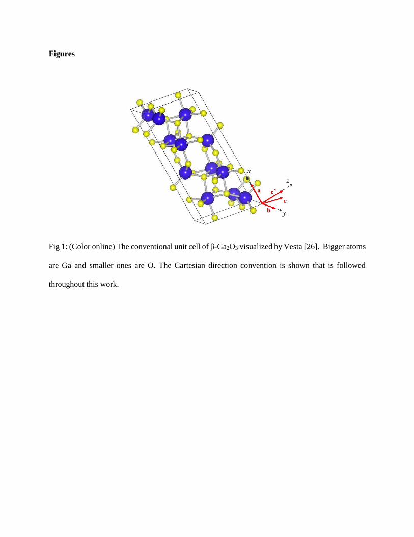
constants scaled by reduced atomic masses, √𝑀𝜅𝑀𝜅′) yields the LO eigen values. Fig. 1 shows
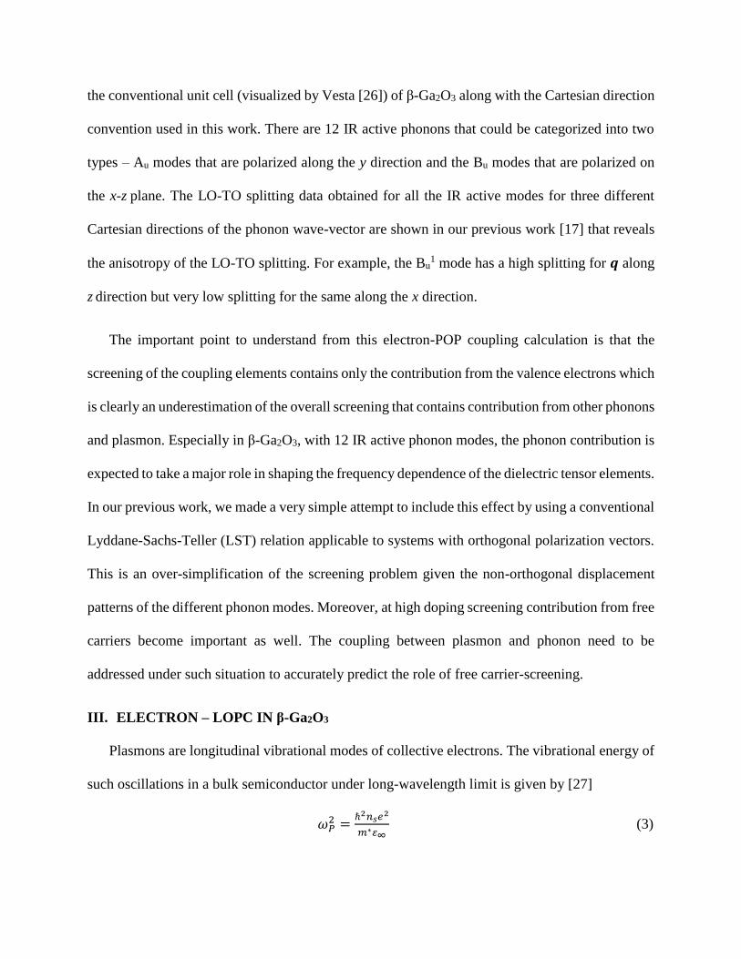
the conventional unit cell (visualized by Vesta [26]) of β-Ga2O3 along with the Cartesian direction
convention used in this work. There are 12 IR active phonons that could be categorized into two
types – Au modes that are polarized along the y direction and the Bu modes that are polarized on
the x-z plane. The LO-TO splitting data obtained for all the IR active modes for three different
Cartesian directions of the phonon wave-vector are shown in our previous work [17] that reveals
the anisotropy of the LO-TO splitting. For example, the Bu1 mode has a high splitting for 𝒒 along
z direction but very low splitting for the same along the x direction.
The important point to understand from this electron-POP coupling calculation is that the
screening of the coupling elements contains only the contribution from the valence electrons which
is clearly an underestimation of the overall screening that contains contribution from other phonons
and plasmon. Especially in β-Ga2O3, with 12 IR active phonon modes, the phonon contribution is
expected to take a major role in shaping the frequency dependence of the dielectric tensor elements.
In our previous work, we made a very simple attempt to include this effect by using a conventional
Lyddane-Sachs-Teller (LST) relation applicable to systems with orthogonal polarization vectors.
This is an over-simplification of the screening problem given the non-orthogonal displacement
patterns of the different phonon modes. Moreover, at high doping screening contribution from free
carriers become important as well. The coupling between plasmon and phonon need to be
addressed under such situation to accurately predict the role of free carrier-screening.
III. ELECTRON – LOPC IN β-Ga2O3
Plasmons are longitudinal vibrational modes of collective electrons. The vibrational energy of
such oscillations in a bulk semiconductor under long-wavelength limit is given by [27]
𝜔𝑃2 =
ℏ2𝑛𝑠𝑒2
𝑚∗∞
(3)
Here, 𝑛𝑠 is the conduction electron density and 𝑚∗ is the electron effective mass. So for practical
doping levels ranging from 1017 /cm3 to 1019 /cm3, the plasmon energy varies from about 10 meV
to 100 meV in β-Ga2O3 considering an isotropic effective mass of 0.3 and an average isotropic
high-frequency dielectric constant of 4.3 as calculated from our DFT and DFPT calculations
respectively. This energy range is same as the range where all the LO phonon energies lie. Hence
for transport calculations and subsequent device applications LO-plasmon coupling (LOPC) is
expected to play a vital role.
A. The LOPC modes at arbitrary wave-vectors
Although the pure plasmon energy is fairly isotropic, the LOPC modes would be highly
anisotropic due to the anisotropy of the LO modes. Hence we compute the LOPC modes for each
wave-vector separately. For a given wave-vector q, the pure LO modes 𝜔𝐿𝑂𝑖 (𝒒) are computed by
diagonalizing the DFPT computed dynamical matrix at the Γ point after adding the macroscopic
polarization (Eq. 2). The effective dielectric constant along the direction of 𝒒 is formulated as
from LO mode polarization and plasmon-pole approximation -
휀𝜔(𝒒) = 휀∞ ∏(𝜔𝑖
𝐿𝑂(𝒒))2
−𝜔2
(𝜔𝑖𝑇𝑂)
2−𝜔2𝑖=1−12 − ∞𝜔𝑃
2
𝜔2 (4)
𝜔𝑖𝑇𝑂 are the corresponding TO mode energies. The valence electron contribution to the dielectric
elements is 휀∞. The plasmon contribution is taken to be present along 𝒒 since plasma oscillation
is a longitudinal oscillation. Note that Eq. 4 already accounts for the displacement patterns of the
modes since the 𝜔𝑖𝐿𝑂(𝒒) is calculated explicitly for each 𝒒. Hence comparing with the work of
Schubert et. al. [15] , the effect of the cosine terms ( Eq. 21(a-d) of [15] ) arising on the net dipole
oscillation strength of the different modes are included in Eq. 4 of this work. So essentially, Eq. 4
of this work is equivalent to Eq. 21(a-d) of [15]. However, as for transport properties we are only
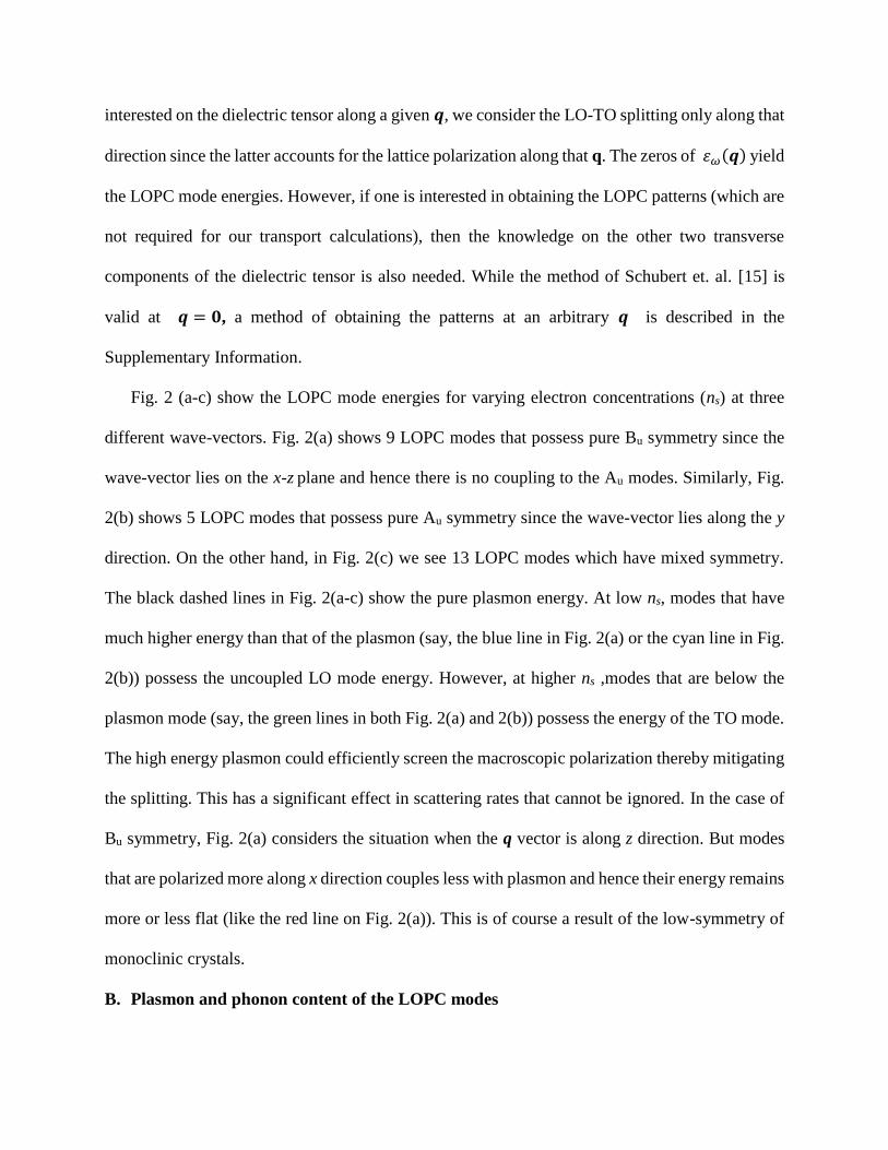
interested on the dielectric tensor along a given 𝒒, we consider the LO-TO splitting only along that
direction since the latter accounts for the lattice polarization along that q. The zeros of 휀𝜔(𝒒) yield
the LOPC mode energies. However, if one is interested in obtaining the LOPC patterns (which are
not required for our transport calculations), then the knowledge on the other two transverse
components of the dielectric tensor is also needed. While the method of Schubert et. al. [15] is
valid at 𝒒 = 𝟎, a method of obtaining the patterns at an arbitrary 𝒒 is described in the
Supplementary Information.
Fig. 2 (a-c) show the LOPC mode energies for varying electron concentrations (ns) at three
different wave-vectors. Fig. 2(a) shows 9 LOPC modes that possess pure Bu symmetry since the
wave-vector lies on the x-z plane and hence there is no coupling to the Au modes. Similarly, Fig.
2(b) shows 5 LOPC modes that possess pure Au symmetry since the wave-vector lies along the y
direction. On the other hand, in Fig. 2(c) we see 13 LOPC modes which have mixed symmetry.
The black dashed lines in Fig. 2(a-c) show the pure plasmon energy. At low ns, modes that have
much higher energy than that of the plasmon (say, the blue line in Fig. 2(a) or the cyan line in Fig.
2(b)) possess the uncoupled LO mode energy. However, at higher ns ,modes that are below the
plasmon mode (say, the green lines in both Fig. 2(a) and 2(b)) possess the energy of the TO mode.
The high energy plasmon could efficiently screen the macroscopic polarization thereby mitigating
the splitting. This has a significant effect in scattering rates that cannot be ignored. In the case of
Bu symmetry, Fig. 2(a) considers the situation when the q vector is along z direction. But modes
that are polarized more along x direction couples less with plasmon and hence their energy remains
more or less flat (like the red line on Fig. 2(a)). This is of course a result of the low-symmetry of
monoclinic crystals.
B. Plasmon and phonon content of the LOPC modes
In order to calculate the electron scattering rates mediated by the LOPC modes we need to
separate out the plasmon and phonon contents for each mode. This is because scattering with pure
plasma does not effectively provide any average momentum relaxation for the ensemble of
electrons rather it just renders exchange of momentum among electrons. In the following we follow
a method originally proposed by Fischetti et. al. [29] for studying coupling between interface
phonons from the dielectric and plasmons in the semiconductor. We compute the plasmon content
in an LOPC mode 𝜈 as
Λ𝜈𝑃(𝒒) =
∏ ((𝜔𝜐𝐿𝑂𝑃𝐶(𝒒))
𝟐−(𝜔𝑖
𝐿𝑂(𝒒))𝟐
)𝒊
∏ ((𝜔𝜐𝐿𝑂𝑃𝐶(𝒒))
𝟐−(𝜔𝑖
𝐿𝑂𝑃𝐶(𝒒))𝟐
)𝒊≠𝜐
(5)
𝜔𝑖𝐿𝑂(𝒒) are the pure LO modes obtained in absence of any plasmon. The total phonon content of
the mode would be 1 − Λ𝜈𝑃(𝒒).
The relative contribution of the individual phonon modes in a given LOPC mode could also
computed under a similar technique –
R𝜈𝐿𝑂𝑗(𝒒) =
∏ ((𝜔𝜐𝐿𝑂𝑃𝐶(𝒒))
𝟐−(𝜔𝑖
𝐿𝑂𝑃𝐶, −𝐿𝑂𝑗(𝒒))𝟐
)𝒊
∏ ((𝜔𝜐𝐿𝑂𝑃𝐶(𝒒))
𝟐−(𝜔𝑖
𝐿𝑂𝑃𝐶(𝒒))𝟐
)𝒊≠𝜐
(6)
Here the 𝜔𝑖𝐿𝑂𝑃𝐶, −𝐿𝑂𝑗(𝒒) are the modes obtained by forming Eq. 4 without the response of the jth
LO mode and then setting its determinant to zero. The net contribution of the jth LO mode in the
LOPC mode 𝜈 would be
Λ𝜈𝐿𝑂𝑗(𝒒) =
R𝜈𝐿𝑂𝑗(𝒒)
∑ R𝜈𝐿𝑂𝑘(𝒒)𝒌
(1 − Λ𝜈𝑃(𝒒)) (7)
Two important sum rules are to be verified here. First one of them is trivial, ∑ Λ𝜈𝐿𝑂𝑗(𝒒)𝑗 +
Λ𝜈𝑃(𝒒) = 1 , which says the total contribution of the plasmon mode and the LO modes to a
particular LOPC mode must be 1. The second one is ∑ Λ𝜈𝐿𝑂𝑗(𝒒)𝜐 = 1 and ∑ Λ𝜈
𝑃(𝒒)𝜐 = 1 which
says the sum of the relative contributions of any LO mode (or the plasmon mode) to all the LOPC
modes must be 1. The sum rules are verified for all the electron densities considered in this work.
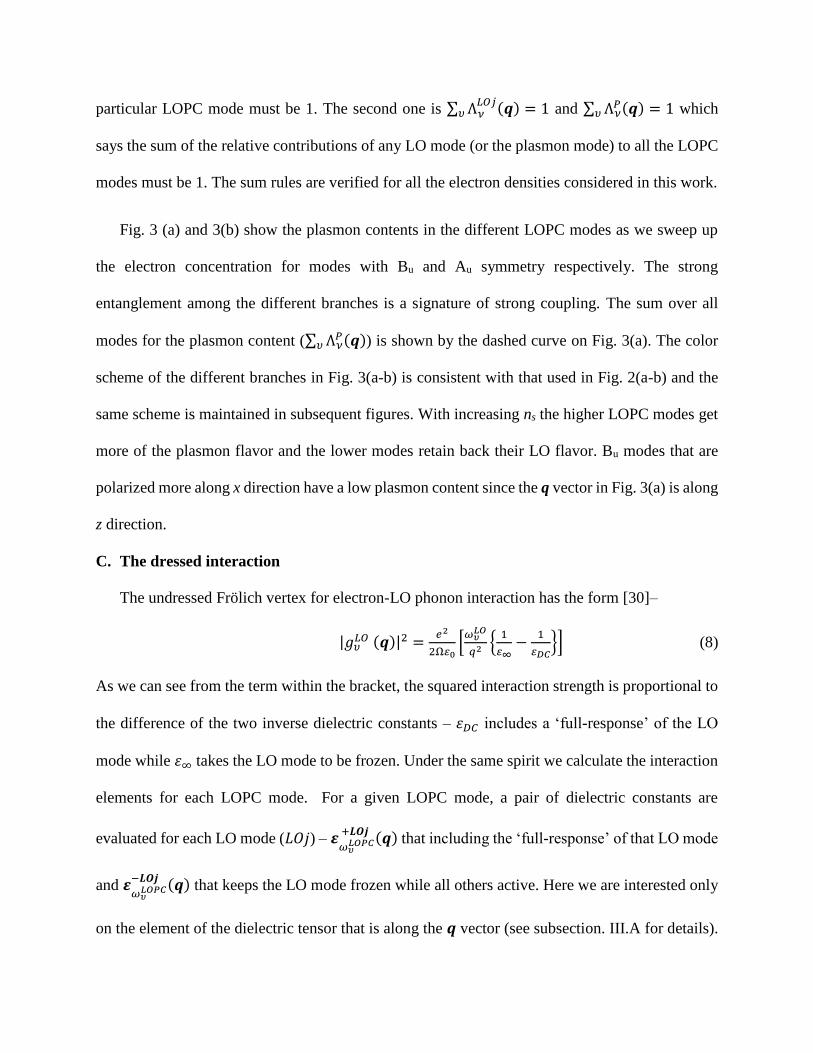
Fig. 3 (a) and 3(b) show the plasmon contents in the different LOPC modes as we sweep up
the electron concentration for modes with Bu and Au symmetry respectively. The strong
entanglement among the different branches is a signature of strong coupling. The sum over all
modes for the plasmon content (∑ Λ𝜈𝑃(𝒒)𝜐 ) is shown by the dashed curve on Fig. 3(a). The color
scheme of the different branches in Fig. 3(a-b) is consistent with that used in Fig. 2(a-b) and the
same scheme is maintained in subsequent figures. With increasing ns the higher LOPC modes get
more of the plasmon flavor and the lower modes retain back their LO flavor. Bu modes that are
polarized more along x direction have a low plasmon content since the q vector in Fig. 3(a) is along
z direction.
C. The dressed interaction
The undressed Frölich vertex for electron-LO phonon interaction has the form [30]–
|𝑔𝜐𝐿𝑂 (𝒒)|2 =
𝑒2
2Ω 0[
𝜔𝜐𝐿𝑂
𝑞2 {1
∞−
1
𝐷𝐶}] (8)
As we can see from the term within the bracket, the squared interaction strength is proportional to
the difference of the two inverse dielectric constants – 휀𝐷𝐶 includes a ‘full-response’ of the LO
mode while 휀∞ takes the LO mode to be frozen. Under the same spirit we calculate the interaction
elements for each LOPC mode. For a given LOPC mode, a pair of dielectric constants are
evaluated for each LO mode (𝐿𝑂𝑗) – 𝜺𝜔𝜐
𝐿𝑂𝑃𝐶 +𝑳𝑶𝒋 (𝒒) that including the ‘full-response’ of that LO mode
and 𝜺𝜔𝜐
𝐿𝑂𝑃𝐶−𝑳𝑶𝒋 (𝒒) that keeps the LO mode frozen while all others active. Here we are interested only
on the element of the dielectric tensor that is along the 𝒒 vector (see subsection. III.A for details).
Note that this type of formulation of the interaction strength includes all the screening (and also
anti-screening) contribution in the long-wavelength. Hence the dressed interaction term could be
cast as –
|𝑔𝐿𝑂𝑃𝐶𝜐, 𝐿𝑂𝑗
(𝒒)|2
=𝑒2
2Ω 0[
𝜔𝜐𝐿𝑂𝑃𝐶(𝒒)
𝑞2 {1
𝜺𝜔𝜐
𝐿𝑂𝑃𝐶−𝑳𝑶𝒋
(𝒒)−
1
𝜺𝜔𝜐
𝐿𝑂𝑃𝐶+𝑳𝑶𝒋
(𝒒)} Λ𝜈
𝐿𝑂𝑗(𝒒)] (9)
In terms of the actual calculations performed, 𝜺𝜔𝜐
𝐿𝑂𝑃𝐶 −𝑳𝑶𝒋 (𝒒) is estimated from Eq. 4 with the
summation running over all i for 𝑖 ≠ 𝑗 and 𝜺𝜔𝜐
𝐿𝑂𝑃𝐶+𝑳𝑶𝒋 (𝒒) is also estimated from Eq. 4 with the
condition on the summation that 𝜔 = 0 for 𝑖 = 𝑗. The anisotropic dependence of the interaction is
completely taken care of under this manifold because all the dielectric elements are formed taking
into account the displacement patterns of the modes.
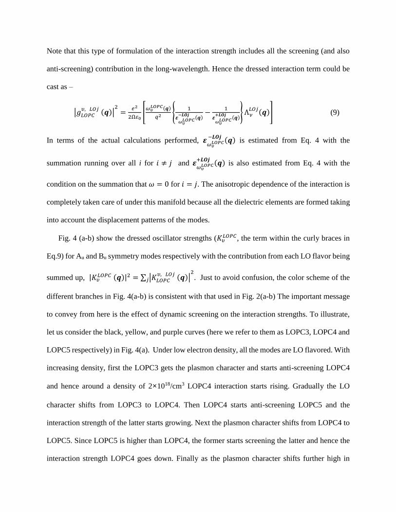
Fig. 4 (a-b) show the dressed oscillator strengths (𝐾𝜐𝐿𝑂𝑃𝐶, the term within the curly braces in
Eq.9) for Au and Bu symmetry modes respectively with the contribution from each LO flavor being
summed up, |𝐾𝜐𝐿𝑂𝑃𝐶 (𝒒)|2 = ∑ |𝐾𝐿𝑂𝑃𝐶
𝜐, 𝐿𝑂𝑗 (𝒒)|
2
𝑗 . Just to avoid confusion, the color scheme of the
different branches in Fig. 4(a-b) is consistent with that used in Fig. 2(a-b) The important message
to convey from here is the effect of dynamic screening on the interaction strengths. To illustrate,
let us consider the black, yellow, and purple curves (here we refer to them as LOPC3, LOPC4 and
LOPC5 respectively) in Fig. 4(a). Under low electron density, all the modes are LO flavored. With
increasing density, first the LOPC3 gets the plasmon character and starts anti-screening LOPC4
and hence around a density of 2×10¹⁸/cm3 LOPC4 interaction starts rising. Gradually the LO
character shifts from LOPC3 to LOPC4. Then LOPC4 starts anti-screening LOPC5 and the
interaction strength of the latter starts growing. Next the plasmon character shifts from LOPC4 to
LOPC5. Since LOPC5 is higher than LOPC4, the former starts screening the latter and hence the
interaction strength LOPC4 goes down. Finally as the plasmon character shifts further high in
energy LOPC5 also gets well screened and its scattering strength goes down as well. So in a
material like β-Ga2O3 with several LO modes, as the plasmon character propagates from one mode
to the other, the screening and anti-screening of the modes shift accordingly. Hence for a given
electron density on mode could be screened while the other could be anti-screened and hence a
generic trend of the electron scattering rates and hence the mobility with an increasing electron
density is not expected. In the next Section while discussing electron mobility this issue is further
explored.
D. Plasmon damping
Plasmons cease to behave as collective excitations in the electron-hole pair continuum (EHC).
This is going to influence the LOPC modes and the dynamic screening depending upon the
magnitude of the wave-vector, q. This damping becomes particularly important for degenerate
doping. We treat this effect (approximately) by turning off the plasmon mode in the EHC. The
upper boundary of EHC is given by [27], 𝜔+(𝑞) =ℏ2𝑘𝐹𝑞
𝑚∗+
ℏ2𝑞2
2𝑚∗, where 𝑘𝐹 is the Fermi wave-
vector calculated at zero temperature. Due to isotropic conduction band minima, the upper
boundary of EHC is taken to be isotropic in β-Ga2O3 and hence the plasmon damping is dependent
only on the magnitude of q. In terms of the actual calculation performed, the plasmon mode is
taken off from the dispersion and dynamic screening calculation whenever, 𝜔𝑃 < 𝜔+(𝑞). The data
shown in Fig. 2, Fig. 3, and Fig. 4 do not take into account the effect of plasmon damping in order
clearly convey the LOPC picture in β-Ga2O3. However, the transport calculations are done
including the effects of the damping. It is to be noted that this damping is different from the finite
temperature plasmon damping arising from electron-phonon interactions that give rise to the
imaginary part of the dielectric function. The latter type of damping is not considered in this work
because that would involve self-consistently finding out the electron relaxation rates and the
imaginary part of the dielectric constant which the authors believe would be extremely challenging
especially for Ga2O3 with so many phonon modes.
E. Electron scattering mediated by the LOPC modes
Having found out the interaction elements we are ready to compute the electron scattering
mediated by the LOPC modes for electron wave-vectors 𝒌. The scattering rate is computed under
Fermi-Golden rule as –
S𝐿𝑂𝑃𝐶(𝒌) = ∑ 𝑤𝒒|𝑔𝐿𝑂𝑃𝐶𝜐, 𝐿𝑂𝑗
(𝒒)|2
𝑗,𝜐,𝒒1
(𝐸𝒌+𝒒−𝐸𝒌 ± 𝜔𝜐𝐿𝑂𝑃𝐶(𝒒)−𝑖𝛿)
(10)
Here 𝐸𝒌 denotes the electron energy at wave-vector 𝒌 and 𝑤𝒒 is the weight of the 𝒒 point from the
Brillouin zone sampling. 𝛿 is a small energy smearing chosen to be 10 meV in this work. We used
an isotropic parabolic electron band which is a very good assumption for β-Ga2O3 near the Γ-point.
However, the scattering rates are computed at each 𝒌 point separately to probe the anisotropy in
the later transport calculation. Fig. 5 (a) shows the electron scattering rate for two levels of electron
concentrations. The scattering rate at a lower electron concentration is higher at lower electron
energies. This is because of the anti-screening of the low energy phonon modes. On the other hand,
at relatively higher electron concentrations the lower energy phonon modes are screened but the
higher energy phonons are anti-screened. This suppresses the scattering rate at lower electron
energies but boosts it up at higher energies. This has a significant role in deciding the electron
mobility.
IV. ELECTRON MOBILITY
The electron mobility is calculated by solving the Boltzmann transport equation (BTE) using
our in-house codes based on Rode’s iterative scheme [31]. Scattering mechanisms included are the
LOPC scattering and the ionized impurity scattering. The ionized impurity scattering rate is
calculated using a simple Brooks-Herring model with an isotropic parabolic electronic band of
effective mass 0.3m0. The trend of mobility is studied with respect to varying electron
concentrations for bulk β-Ga2O3 and for two-dimensional electron gas formed at heterojunctions
like AlxGa2-xO3/Ga2O3.
A. Iterative BTE solver
The iterative BTE solver goes beyond the relaxation time approximation as it takes care of the
inelasticity of the scattering which is particularly important at low electron energies. The electronic
distribution function, 𝑓(𝑘), is split in two parts as 𝑓(𝒌) = 𝑓0(𝑘) + 𝑓′(𝑘) cos 𝜃. While the
equilibrium part 𝑓0(𝑘) is the Fermi-Dirac function, the non-equilibrium part 𝑓′(𝑘) is evaluated
self-consistently using the scattering information as discussed below. The angle 𝜃 is between the
applied electric field and the electron wave-vector k. 𝑓′(𝑘) under electric field 𝑭 is calculated as
𝑓𝑖+1′(𝑘) =
(𝑆𝑖𝐼𝑁(𝑘)−
𝑒𝑭
ℏ.∇𝒌𝑓0(𝑘))
(𝑆𝑂𝑈𝑇(𝑘)+1
𝜏𝑒𝑙)
(11)
Here the subscripts denote the iteration number in the self-consistent scheme. 𝑆𝑂𝑈𝑇(𝑘) and
𝑆𝑖𝑛(𝑘) are the net out-scattering and net in-scattering terms respectively from an electronic wave-
vector 𝑘. Note that, although a scalar notation of the wave-vector is used for the arguments 𝑆𝑂𝑈𝑇
and 𝑆𝑖𝑛 in Eq. 11, they are calculated along each three directions separately and hence Eq. 11 is
for any given direction at a time. The anisotropic effects that are supposed to arise from the
anisotropic electron-LOPC is inherent in the out-scattering and in-scattering terms while
evaluating them using Fermi-Golden rule. However, anisotropy from the band-structure (which is
very minimal in β-Ga2O3) is not incorporated in this formulation. 𝑆𝑖𝑛(𝑘) is dependent upon 𝑓′(𝑘)
by
𝑆𝑖𝑛(𝑘) = ∫ 𝑋𝑓′(𝑘′)[𝑃𝒌′→𝒌(1 − 𝑓0(𝑘)) + 𝑃𝒌→𝒌′𝑓0(𝑘)] 𝑑𝒌′ (12)
Here, 𝑃𝒌′→𝒌 is the Fermi-Golden transition rate and 𝑋 is the cosine of the angle between 𝒌′ and
𝒌. Eq. 11 and Eq. 12 form a self-consistent pair which is solved iteratively starting from the initial
condition given by RTA, 𝑓0′(𝑘′) = −
𝑒𝑭
ℏ. ∇𝒌𝑓0(𝑘).
Fig. 5(b) shows the antisymmetric part ( 𝑓′(𝑘) ) of the distribution function after the
convergence in the iteration has been achieved. The small discontinuities in the distribution
functions are results of the onset of emission of the dominant LOPC modes. Under a low electron
concentration such onset occurs at a lower energy because the lower LOPC modes are anti-
screened while with increasing electron concentration the onset point shifts to higher energies since
the anti-screening behavior shifts to higher LOPC modes. On the other hand the symmetric part of
the distribution does not contribute to net drift mobility. The electron mobility is calculated from
the anti-symmetric part of the distribution function as 𝜇𝑛 =∑ 𝑣(𝒌)𝑓′(𝒌)(cos 𝜃)2
𝒌
∑ 𝑓0(𝒌)𝒌 where 𝑣(𝒌) is the
group velocity of the electrons at a wave-vector 𝒌 and 𝑣(𝒌) cos 𝜃 represents the drift velocity
along the electric-field.
B. Bulk mobility and anisotropy
The room temperature bulk mobility is calculated under two conditions – with ionized impurity
scattering and without that. The electron concentration is taken to be same as the dopant
concentration for the former case. The calculated mobility is shown in Fig. 6. For the case without
any impurity scattering the mobility initially shows a decline which is attributed to the anti-
screening of low energy LOPC modes and hence a stronger scattering strength. At higher doping
the mobility increases with increasing doping due to strong screening of the LOPC modes. It is to
be noted here that the screening in [18] is essentially static which is good under high electron
densities when the plasmon energy is higher than all the LO energies and hence the dielectric
constant can be represented by static limits like Thomas-Fermi model. However, at moderate
electron densities like 1018 /cm3, some of the LO modes are screened while others are anti-screened
which would have consequences on the electron transport and mobility. Using a dynamic model
is crucial to capture the interplay of screening and anti-screening. As seen from [18], the phonon
limited electron mobility shows an increase at moderate electron densities due to free-carrier
screening which is correct under the static limit. This work augments that fact by adding the
contribution of anti-screening. In the case when ionized impurity scattering is present (circles in
Fig. 6), the enhancement of mobility at higher doping is negligible since the scattering due to
impurities compensates the reduction of LOPC mediated scattering under strong screening. The
mobility, including ionized impurity scattering, at an electron concentration of 5×10¹⁹/cm3 is about
182 cm2/V.s. However for devices where the electronic channel is separated from the dopants an
intermediate mobility (between the circles and triangles) is to be expected due to the presence of
remote ionized impurity scattering which is discussed next during 2DEG mobility analysis.
Next we turn to discuss the anisotropy of the computed mobility in the two different directions.
As seen from Fig. 6 the mobility is higher along the y direction compared to that in the z direction.
The anisotropy is about 20% at a moderate doping. Such anisotropy is experimentally observed
[32], but its origin is not clearly understood since it is well known that the electronic bands in β-
Ga2O3 near the Γ point is isotropic. We attribute this anisotropy of the long-range interaction
between the electrons and the LO modes (even in absence of any plasmon). The dominating Bu1
mode as found in our previous work has a high projection of polarization along the z axis. Now
low energy electrons moving along the z direction will get scattered by phonons with wave-vector
along the z direction. This idea is shown on Fig. 7(a). To better convey the idea behind the origin
of the anisotropy we carried out a Monte Carlo simulation to probe the emission rates of the
different phonons mediated by the long-range interactions with electrons. No plasmon is
considered in the MC simulation for simplicity and that does not affect the fundamental concept
behind this anisotropy. Fig. 7(b) shows the emission rates of the three modes Bu1, Au
2, and Bu6
under an external electric field of 5×10⁶ V/m applied along the z direction. The emission rate of
the Bu1 is higher because of the stronger interaction. The Bu
6 mode has a relatively higher energy
and only a few electrons have enough energy under this electric-field to emit Bu6 modes. Now as
the electric field is enhanced, as shown in Fig. 7(c), the emission rate of the Bu6 mode increases
because electrons gain enough energy. However, although Au2 has a lower energy than Bu
6, its
emission rate increases by a smaller amount than Bu6. This is because the for an applied electric
field along the z direction the momentum of the electrons are more incline along the z direction
and hence they couple more with phonons with wave-vectors along z. This explains the
experimentally observed [32] anisotropy in electron mobility. Hence this anisotropy completely
follows from the anisotropy of the long-range electron-phonon interaction and on contrary to most
conventional semiconductors, this anisotropy is not a result of any conduction band anisotropy
rather it is a clear signature of the low-symmetry of the monoclinic β-Ga2O3 crystal that results to
anisotropic LO-TO splitting. The anisotropy decreases with increasing impurity scattering (see
Fig. 6) since the latter is isotropic.
C. 2DEG mobility
Two-dimensional electron gas in β-Ga2O3 has been very recently demonstrated experimentally
[33]. Theoretical mobility limits are not well known yet. Here we study the mobility of 2DEG
formed in the inversion layer of a simple AlxGa2-xO3/Ga2O3 (ALGO/GO) heterojunction with
varying electron concentration. The typical structure is shown in the inset of Fig. 8 where the
2DEG is situated at a distance d from the dopants. The dopants are taken to be as a sheet charge
density behaving like a δ Coulomb potential and it is assumed that the 2DEG density at the channel
is same as the sheet charge density of the dopants (such assumption could be relaxed by using a
Poisson solver and is not addressed here for the sake of clearly conveying the trend of the mobility
with increasing electron concentration). The scattering rate from such remote impurity (RI) center
is modelled using a statically screened Coulomb interaction [34] –
𝑆𝑅𝐼 =𝑁𝐼𝑒4𝑚∗
4𝜋ℏ3( 𝑠+ 𝑠′)
2 ∫(1−cos 𝜑)
(𝑞2+𝑞𝑇𝐹2)
𝐴2(𝑞) 𝑑𝜃2𝜋
0 (13)
Here 𝑁𝐼 is the surface charge density present at the interface, 휀𝑠 and 휀𝑠′ are the static dielectric
constants of the electron channel (in GO) and the dopant location (ALGO). We considered 휀𝑠 =
휀𝑠′ , which is not a bad approximation for small aluminum content in ALGO. 𝑞𝑇𝐹 is the two
dimensional Thomas-Fermi (TF) screening wave-vector given by [34] 2
𝑎𝐵∗ , where 𝑎𝐵
∗ is the
effective Born radius. Note that he 2D TF wave-vector is independent of the electron
concentration. 𝐴(𝑞) is the overlap function between the confined out-of-plane envelope function
of the electron gas and the exponentially decaying Coulomb potential envelope from the remote
impurities. The envelope function for the 2DEG is taken as the usual Fang-Howard form [34] with
an average inversion layer thickness of 5 nm. The (1 − cos 𝜑) term in the numerator of Eq. 13
accounts for the effective momentum relaxation with 𝜑 being the angle between the in-plane
electron wave-vector (k) and q. Due to the elastic nature of the impurity scattering, 𝑞 = 2𝑘 sin𝜑
2.
The LOPC scattering formulation in the case of 2DEG follows the same steps as that for the
bulk case except that the plasmon energy is modified by the first order term, of the plasmon
dispersion for a 2DEG, 𝜔𝑃2 =
ℏ2𝑛𝑠𝑒2𝑞
𝑚∗∞
, as shown by Stern [35]. The 2DEG is taken to be in the 1st
sub-band and no LOPC mode mediated inter-subband transition is considered due to high enough
energy gap with the second subband. The confined direction is taken to be the y direction. This
implies that only the Bu character LOPC modes are able to cause the scattering under this
circumstance since momentum conservation will not allow the LOPC modes with wave-vector
along the y direction to cause intra-subband transition. The computed mobility along the z
direction is shown on Fig. 8 for several cases. Like the bulk case, the mobility improves with
increased electron concentration due to enhanced screening of the LOPC modes. The anti-
screening behavior is not observed since that occurs at a lower electron concentration than what is
shown in Fig. 8. The mobility at a 2DEG density of 5×10¹² /cm2, when the RI center is at the
interface, is around 418 cm2/V.s which is more than 2X higher than the bulk case. As the RI center
moves away from the interface the mobility improves on the higher ns side due to less scattering
by the RI. Reduction of the phase space for final state after scattering and the remoteness of the
impurities are responsible for the improvement in mobility. The error bars in Fig. 8 are showing a
±10% offset that might arise from issues like dielectric mismatch at the interface, truncating the
plasmon dispersion after first-order, and any numerical inaccuracies. In reality this δ doping is
only a few nanometers far from the interface in order to maximize the electron concentration in
the channel. So as seen from Fig. 8 it is expected that the mobility would be close to 1000 cm2/Vs
in the absence of any other scattering mechanisms that could potentially originate from surface-
roughness, alloy disorder, or remote interface phonons.
V. CONCLUSION
We have calculated the electron density dependence of the mobility of β-Ga2O3 in bulk and
2DEG form. The enhanced screening at higher electron densities provide promise for improved
mobility which is important for device operation. The interplay of screening and anti-screening of
the LOPC modes at intermediate electron densities gives rise to interesting trends in the electron
mobility. The anisotropy of the electron mobility is explained by an anisotropic polar phonon
emission picture produced by Monte Carlo simulations. The 2DEG mobility shows more than 2X
improvement than bulk mobility. Further study on the 2DEG mobility is required by changing the
separation of the dopants and the 2DEG. Also the confinement direction can be changed from y to
z for studying any further improvement of mobility.
The authors acknowledge the support from the National Science Foundation (NSF) grant
(ECCS 1607833). The authors also acknowledge the excellent high performance computing cluster
provided by the Center for Computational Research (CCR) at the University at Buffalo.
References
[1] M. Higashiwaki, K. Sasaki, T. Kamimura, M. Hoi Wong, D. Krishnamurthy, A. Kuramata, T. Masui, and S. Yamakoshi: Depletion-mode Ga2O3 metal-oxide-semiconductor field-effect transistors on β-Ga2O3 (010) substrates and temperature dependence of their device characteristics, Appl. Phys. Lett. 103, 123511 (2013). [2] M. Higashiwaki, K. Sasaki, A. Kuramata, T. Masui, and S. Yamakoshi: Gallium oxide (Ga2O3) metal-semiconductor field-effect transistors on single-crystal β-Ga2O3 (010) substrates, Appl. Phys. Lett. 100, 013504 (2012). [3] M. Higashiwaki, K. Sasaki, H. Murakami, Y. Kumagai, A. Koukitu, A. Kuramata, T. Masui, and S. Yamakoshi: Recent progress in Ga2O3 power devices, Semicon. Sci. Tech. 31, 034001 (2016). [4] T. Oishi, Y. Koga, K. Harada, and M. Kasu: High-mobility β- Ga2O3 (201) single crystals grown by edge-defined film-fed growth method and their Schottky barrier diodes with Ni contact, Appl. Phys. Express 8, 031101 (2015). [5] K.S.e. al, Ga2O3 Schottky Barrier Diodes Fabricated by Using Single-Crystal β–Ga2O3 (010) Substrates, IEEE Elec Dev. Lett, 34 (2013). [6] M. Higashiwaki : Ga2O3 Schottky Barrier Diodes with n- Ga2O3 Drift Layers Grown by HVPE, IEEE Dev. Res. Conf., 29-30 (2015). [7] T. Oshima, T. Okuno, N. Arai, N. Suzuki, S. Ohira and S. Fujita: Vertical Solar-Blind Deep-Ultraviolet Schottky Photodetectors Based on β- Ga2O3 Substrates, Appl. Phys. Exp., 1 011202 (2008). [8] H. He, R. Orlando, M.A. Blanco, R. Pandey, E. Amzallag, I. Baraille, and M. Rérat: First-principles study of the structural, electronic, and optical properties of Ga2O3 in its monoclinic and hexagonal phases, Phys. Rev. B 74, 195123 (2006). [9] C. Janowitz, V. Scherer, M. Mohamed, A. Krapf, H. Dwelk, R. Manzke, Z. Galazka, R. Uecker, K. Irmscher, R. Fornari, M. Michling, D. Schmeißer, J.R. Weber, J.B. Varley and C.G. VandeWalle: Experimental electronic structure of In2O3and Ga2O3, New J. Phys. 13, 085014 (2011). [10] H. Peelaers, C.G. Van de Walle, Brillouin zone and band structure of β- Ga2O3, Phys. Stat. Solid. (b), 252 828-832 (2015). [11] Y. Zhang, J. Yan, G. Zhao, and W. Xie: First-principles study on electronic structure and optical properties of Sn-doped β- Ga2O3, Physica B 405 , 3899-3903 (2010). [12] K. Sasaki, M. Higashiwaki, A.Kuramata, T.Masui, and S. Yamakoshi: β- Ga2O3 Schottky Barrier Diodes Fabricated by Using Single-Crystal β- Ga2O3 (010) Substrates. IEEE Elec. Dev. Lett. 34, 493-495, (2013). [13] B. Liu, M. Gu, and X. Liu: Lattice dynamical, dielectric, and thermodynamic properties of β- Ga2O3 from first principles, Appl. Phys. Lett., 91 ,172102 (2007).
[14] M.D. Santia, N. Tandon, and J.D. Albrecht: Lattice thermal conductivity in β- Ga2O3 from first principles, Appl. Phys. Lett. 107, 041907 (2015). [15] M. Schubert, R. Korlacki, S. Knight, T. Hofmann, S. Schöche, V. Darakchieva, E. Janzén, B. Monemar, D. Gogova, Q.T. Thieu, R. Togashi, H. Murakami, Y. Kumagai, K. Goto, A. Kuramata, S. Yamakoshi, and M. Higashiwaki: Anisotropy, phonon modes, and free charge carrier parameters in monoclinic β-gallium oxide single crystals, Phys. Rev. B 93, 125209 (2016). [16] A. Parisini, and R. Fornari: Analysis of the scattering mechanisms controlling electron mobility in β- Ga2O3 crystals, Semicond. Sci. Tech. 31, 035023 (2016) . [17] K. Ghosh, and U. Singisetti: Ab initio calculation of electron–phonon coupling in monoclinic β- Ga2O3 crystal, Appl. Phys. Lett. 109, 072102 (2016). [18] Y. Kang, K. Krishnaswamy, H. Peelaers, C.G. VandeWalle: Fundamental limits on the electron mobility of β- Ga2O3, J. Phys. Cond. Mat. 29, 234001(2017). [19] N.Ma, A.Verma, Z.Guo, T.Luo, and D.Jena: Intrinsic Electron Mobility Limits in β- Ga2O3, arXiv preprint arXiv:1610.04198, (2016). [20] C. Verdi and F. Giustino, Frohlich Electron-Phonon Vertex from First Principles, Phys. Rev. Lett. 115, 176401 (2015). [21] S. Baroni, S.D. Gironcoli, A.D. Corso: Phonons and related crystal properties from density-functional perturbation theory, Reviews of Modern Physics 73 515-562, (2001). [22] P. Giannozzi, S. Baroni, N. Bonini, M. Calandra, R. Car, C. Cavazzoni, D. Ceresoli, G.L. Chiarotti, M. Cococcioni, I. Dabo, A. Dal Corso, S. de Gironcoli, S. Fabris, G. Fratesi, R. Gebauer, U. Gerstmann, C. Gougoussis, A. Kokalj, M. Lazzeri, L. Martin-Samos, N. Marzari, F. Mauri, R. Mazzarello, S. Paolini, A. Pasquarello, L. Paulatto, C. Sbraccia, S. Scandolo, G. Sclauzero, A.P. Seitsonen, A. Smogunov, P. Umari, and R.M. Wentzcovitch, : QUANTUM ESPRESSO: a modular and open-source software project for quantum simulations of materials, J. Phys. Cond. Mat. 21, 395502 (2009). [23] J. Noffsinger, F. Giustino, B.D. Malone, C.-H. Park, S.G. Louie, M.L. Cohen, EPW: A program for calculating the electron–phonon coupling using maximally localized Wannier functions, Comp. Phys. Comm. 181, 2140-2148 (2010). [24] F. Giustino, M.L. Cohen, and S.G. Louie: Electron-phonon interaction using Wannier functions, Phys. Rev. B 76, 165108 (2007). [25] X. Gonze, and C. Lee: Dynamical matrices, Born effective charges, dielectric permittivity tensors, and interatomic force constants from density-functional perturbation theory, Phys. Rev. B 55, 10355 (1997). [26] K. Momma, and F. Izumi: VESTA 3 for three-dimensional visualization of crystal, volumetric and morphology data, J Appl Crystal 44, 1272-1276 (2011). [27] K. Diff, and K.F. Brennan: Theory of electron‐plasmon‐scattering rate in highly doped bulk semiconductors, J Appl. Phys. 69, 3097-3103 (1991). [28] R.H. Lyddane, R.G. Sachs, and E. Teller: On the Polar Vibrations of Alkali Halides, Phys. Rev. 59, 673-676 (1941). [29] M.V. Fischetti, D.A. Neumayer, and E.A. Cartier: Effective electron mobility in Si inversion layers in metal–oxide–semiconductor systems with a high-κ insulator: The role of remote phonon scattering, J. Appl. Phys. 90, 4587-4608 (2001). [30] H. Fröhlich, Electrons in lattice fields, Adv. Phys., 3 (1954) 325-361. [31] D. Rode, Low-field electron transport, Semiconduct. Semimet. 10, 1-89 (1975). [32] M.H. Wong, K. Sasaki, A. Kuramata, S. Yamakoshi, M. Higashiwaki: Electron channel mobility in silicon-doped Ga2O3 MOSFETs with a resistive buffer layer, Jap. J Appl. Phys, 55 ,1202B1209 (2016). [33] S. Krishnamoorthy, Z. Xia, C. Joishi, Y. Zhang, J. McGlone, J. Johnson, M. Brenner, A.R. Arehart, J. Hwang, S. Lodha, S. Rajan, Modulation-doped β-(Al0.2Ga0.8)2O3/ Ga2O3 field-effect transistor, Appl. Phys. Lett. 111, 023502 (2017).
[34] W. Walukiewicz, H. E. Ruda, J. Lagowski, H. C. Gatos, Electron mobility in modulation-doped heterostructures. Phys. Rev. B 30, 4571 (1984). [34] T. Ando, A.B. Fowler, F. Stern, Electronic properties of two-dimensional systems, Rev. Mod. Phys. 54, 437-672 (1982). [35] F. Stern, Polarizability of a Two-Dimensional Electron Gas, Phys. Rev. Lett. 18, 546-548 (1967).
Figures
Fig 1: (Color online) The conventional unit cell of β-Ga2O3 visualized by Vesta [26]. Bigger atoms
are Ga and smaller ones are O. The Cartesian direction convention is shown that is followed
throughout this work.
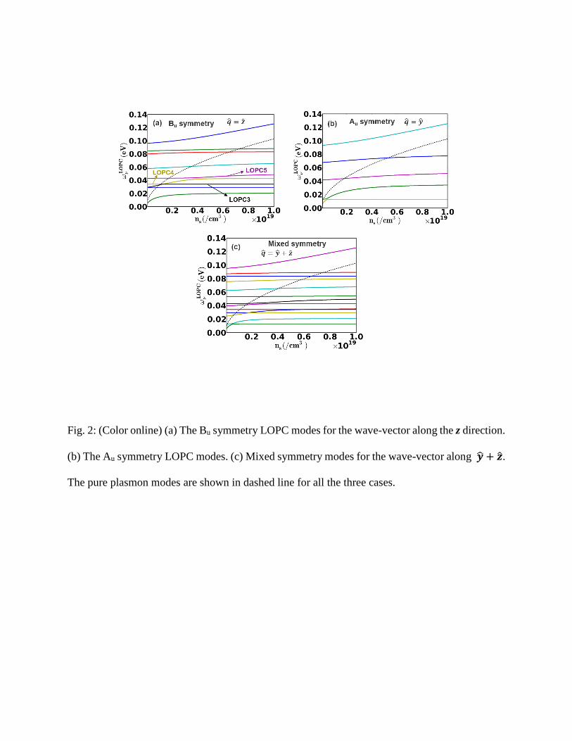
Fig. 2: (Color online) (a) The Bu symmetry LOPC modes for the wave-vector along the z direction.
(b) The Au symmetry LOPC modes. (c) Mixed symmetry modes for the wave-vector along �̂� + �̂�.
The pure plasmon modes are shown in dashed line for all the three cases.
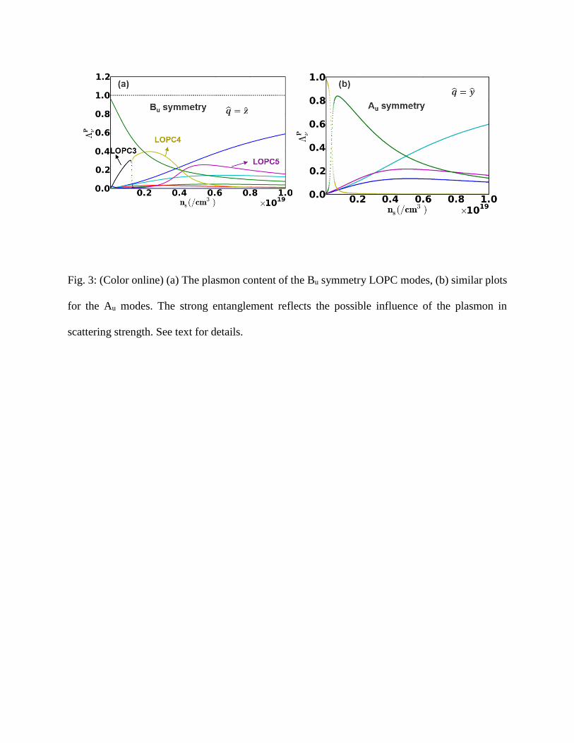
Fig. 3: (Color online) (a) The plasmon content of the Bu symmetry LOPC modes, (b) similar plots
for the Au modes. The strong entanglement reflects the possible influence of the plasmon in
scattering strength. See text for details.

Fig. 4: (Color online) (a) The dynamically screened oscillation strength of the Bu symmetry LOPC
modes, (b) similar plots for the Au modes.
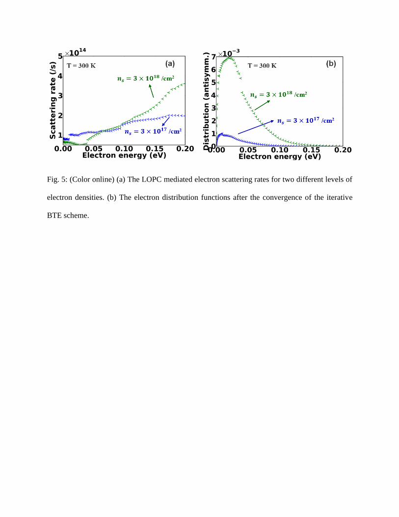
Fig. 5: (Color online) (a) The LOPC mediated electron scattering rates for two different levels of
electron densities. (b) The electron distribution functions after the convergence of the iterative
BTE scheme.
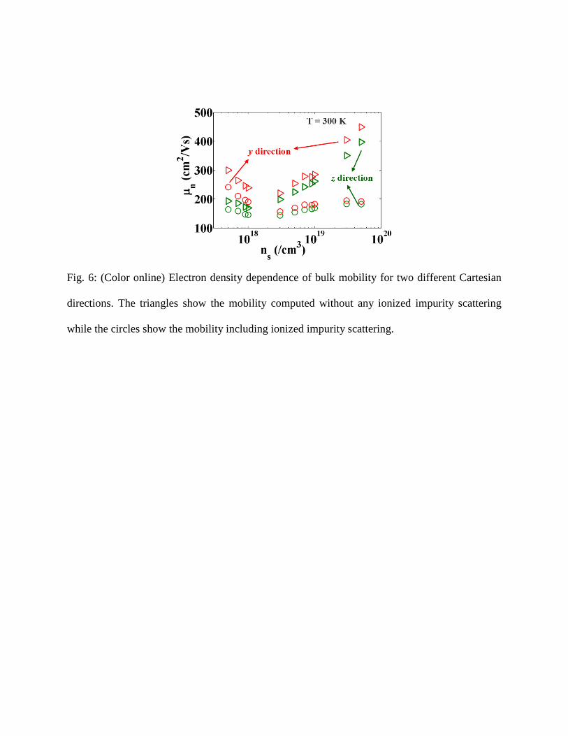
Fig. 6: (Color online) Electron density dependence of bulk mobility for two different Cartesian
directions. The triangles show the mobility computed without any ionized impurity scattering
while the circles show the mobility including ionized impurity scattering.

Fig. 7: (Color online) (a) The momentum conservation requires low energy electrons to be
scattered by phonons whose wave-vectors are inclined towards (opposite) to the electron wave-
vectors. (b) Emission rate of three IR active phonons mediated by long-range interaction with
electrons under an external applied field of 5 × 10⁶V/m. (c) Same plots when the applied field is
2 × 10⁷ V/m.
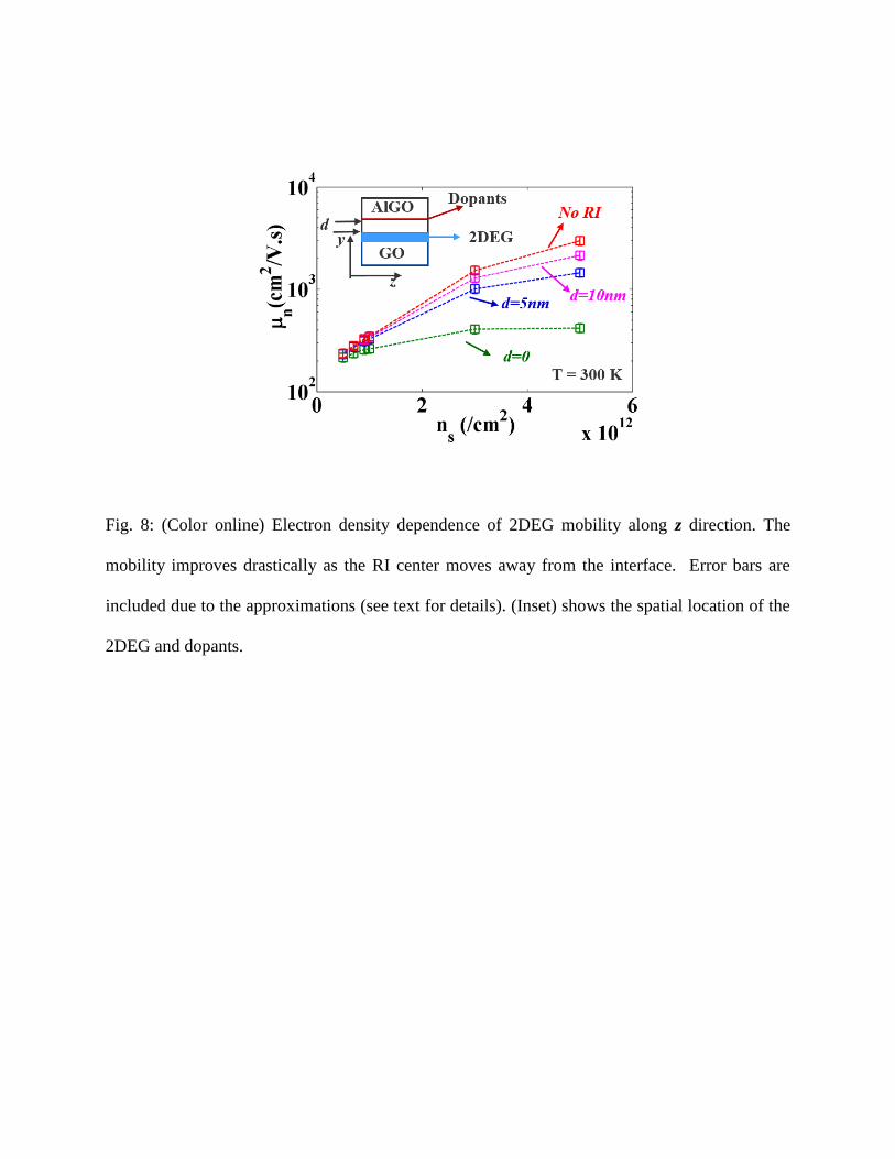
Fig. 8: (Color online) Electron density dependence of 2DEG mobility along z direction. The
mobility improves drastically as the RI center moves away from the interface. Error bars are
included due to the approximations (see text for details). (Inset) shows the spatial location of the
2DEG and dopants.
Related Documents