S.K.R.ENGINEERING COLLEGE AGARMEL – 602 103 (TELUGU MINORITY INSTITUTION) (APPROVED BY AICTE & AFFILIATED TO ANNA UNIVERSITY) (ISO 9001: 2000 CERTIFIED INSTITUTION) DEPARTMENT OF ELECTRONICS AND COMMUNICATION ENGINEERING TWO MARKS QUESTIONS & ANSWERS EC2151 -- ELECTRIC CIRCUITS AND ELECTRON DEVICES 1

ELECTRON DEVICES AND CIRCUITS: 2 Marks q & A
Nov 15, 2014
2 MARKS Q AND A FOR EDC
Welcome message from author
This document is posted to help you gain knowledge. Please leave a comment to let me know what you think about it! Share it to your friends and learn new things together.
Transcript
S.K.R.ENGINEERING COLLEGEAGARMEL – 602 103
(TELUGU MINORITY INSTITUTION)(APPROVED BY AICTE & AFFILIATED TO ANNA UNIVERSITY)
(ISO 9001: 2000 CERTIFIED INSTITUTION)
DEPARTMENT OF ELECTRONICS AND COMMUNICATION ENGINEERING
TWO MARKS QUESTIONS & ANSWERS
EC2151 -- ELECTRIC CIRCUITS AND ELECTRON DEVICES
1
4 0 0 100
SYLLABUSEC2151- ELECTRIC CIRCUITS AND ELECTRON DEVICES
(For ECE, CSE, IT and Biomedical Engg. Branches)
UNIT I CIRCUIT ANALYSIS TECHNIQUES 12 Kirchoff’s current and voltage laws – series and parallel connection of independent sources – R, L and C – Network Theorems – Thevenin, Superposition, Norton, Maximum power transfer and duality – Star-delta conversion. UNIT II TRANSIENT RESONANCE IN RLC CIRCUITS 12 Basic RL, RC and RLC circuits and their responses to pulse and sinusoidal inputs – frequency response – Parallel and series resonances – Q factor – single tuned and double tuned circuits. UNIT III SEMICONDUCTOR DIODES 12 Review of intrinsic & extrinsic semiconductors – Theory of PN junction diode – Energy band structure – current equation – space charge and diffusion capacitances – effect of temperature and breakdown mechanism – Zener diode and its characteristics. UNIT IV TRANSISTORS 12 Principle of operation of PNP and NPN transistors – study of CE, CB and CC configurations and comparison of their characteristics – Breakdown in transistors – operation and comparison of N-Channel and P-Channel JFET – drain current equation – MOSFET – Enhancement and depletion types – structure and operation – comparison of BJT with MOSFET – thermal effect on MOSFET. UNIT V SPECIAL SEMICONDUCTOR DEVICES
(Qualitative Treatment only) 12 Tunnel diodes – PIN diode, varactor diode – SCR characteristics and two transistor equivalent model – UJT – Diac and Triac – Laser, CCD, Photodiode, Phototransistor, Photoconductive and Photovoltaic cells – LED, LCD.
TOTAL: 60 PERIODS
TEXT BOOKS:
1. Joseph A. Edminister, Mahmood, Nahri, “Electric Circuits” – Shaum series,Tata McGraw Hill, (2001)
2. S. Salivahanan, N. Suresh kumar and A. Vallavanraj, “Electronic Devices and Circuits”,Tata McGraw Hill, 2nd Edition, (2008).
3. David A. Bell, “Electronic Devices and Circuits”, Oxford University Press, 5th Edition, (2008). REFERENCES:
1. Robert T. Paynter, “Introducing Electronics Devices and Circuits”, Pearson Education, 7 th Education, (2006).
2. William H. Hayt, J.V. Jack, E. Kemmebly and steven M. Durbin, “Engineering Circuit Analysis”,Tata McGraw Hill, 6th Edition, 2002.
3. J. Millman & Halkins, Satyebranta Jit, “Electronic Devices & Circuits”,Tata McGraw Hill, 2 nd
Edition, 2008.
2

UNIT – IELECTRIC CIRCUITS AND ELECTRON DEVICES
1. What is charge?The charge is an electrical property of the atomic particles of which matter consists. The unit of charge is the coulomb.
2. Define current?The flow of free electrons in a metal is called electric current. The unit of current is the ampere. Current (I) = Q/t, Where Q is total charge transferred & T is time required for transfer of charge.
3. What is voltage?The potential difference between two points in an electric circuit called voltage. The unit of voltage is volt. It is represented by V OR v.
Voltage = W/Q = workdone/Charge
4. Define power.The rate of doing work of electrical energy or energy supplied per unit time is called the power. The power denoted by either P of p. It is measured in Watts. (W).
Power = work done in electric circuit/TimeP = dw/dt = dw/dq.dq/dt
P = VI
5. What is network?Interconnection of two or more simple circuit elements is called an electric network.
6. Distinguish between a branch and a node of a circuit.A part of the network which connects the various points of the network with one another is called a branch. A point at which two or more elements are jointed together is called node.
7. Distinguish between a mesh and a Loop of a circuit.A mesh is a loop that does not contain other loops. All meshed are loops. But all loops are not meshes. A loop is any closed path of branches.
8. Define active and passive elements.The sources of energy are called active element.Example: voltage source, current source.The element which stores or dissipates energy is called passive element.Example: Resistor, Inductor, Capacitor.
9. Define unilateral and bilateral elements.In unilateral element, voltage – current relation is not same for both the direction.Example: Diode, Transistors.In bilateral element, voltage – current relation is same for both the direction.Example: Resistor
3
10. Define linear and non-linear elements.If the element obeys superposition principle, then it is said to be linear elements.Example: Resistor.If the given network is not obeying superposition principle then it is said to be non linear elements.Example: Transistor, Diode.
11. Define Lumped and distributed elements.Physically separable elements are called Lumped element.Example : Resistor, Capacitor, Inductor.A distributed element is one which is not separable for electrical purpose.Example : Transmission line has distributor resistance, capacitance and inductance.
12. How are the electrical energy sources classified?The electrical energy sources are classified into:1. Ideal voltage source 2. Ideal current source.
13. Define an ideal voltage source.The voltage generated by the source does not vary with any circuit quantity. It is only a function of time. Such a source is called an ideal voltage source.
14. Define an ideal current source.The current generated by the source does not vary with any circuit quantity.It is only a function of time. Such a source is called as an ideal current source.
15. What are independent source?Independent sources are those in which, voltage and current are independent and are not affected by other part of the circuit.
16. What are dependent sources?Dependent sources are those in which source voltage or current is not fixed, but is dependent on the voltage or current existing at some other location in the circuit.
17. What are the different types of dependent or controlled sources?1. Voltage Controlled Voltage Sources (VCVS)2. Current Controlled Voltage Sources (CCVS)3. Voltage Controlled Current Sources (VCCS)4. Current Controlled Current Sources (CCCS)
18. What is resistance?It is the property of a substance which opposes the flow of current through it. The resistance of element is denoted by the symbol “R”. It is measured in Ohms.
R = PL / A Ω
4

19. Write down the V-I relationship of circuit elements.
Circuit Element
Voltage Current Power
Resistance V = iR i = V / R P = vi
Inductance V = L di /dt i = 1/L ∫ vdt P = Li di / dt
Capacitance V = 1/c ∫ idt i = C dv / dt P = CV dv / dt
20. What is average value?It is defined as area under one complete cycle to period.The average value of the sine wave is the total area under the half-cycle curve divided by the distance of the curve.
Area under one complete cycleAverage value = _____________________________
Period
21. Define R.M.S. value.The r.m.s value may be determined by taking the mean of the squares of the instantaneous value of current over one complete cycle.
(Area under hatched line) ²
RMS = ______________________Period
22. Define form factor.The ratio of RMS value to the average value is called the Form factor.
RMS valueForm factor (Kf) = ______________
Average Value
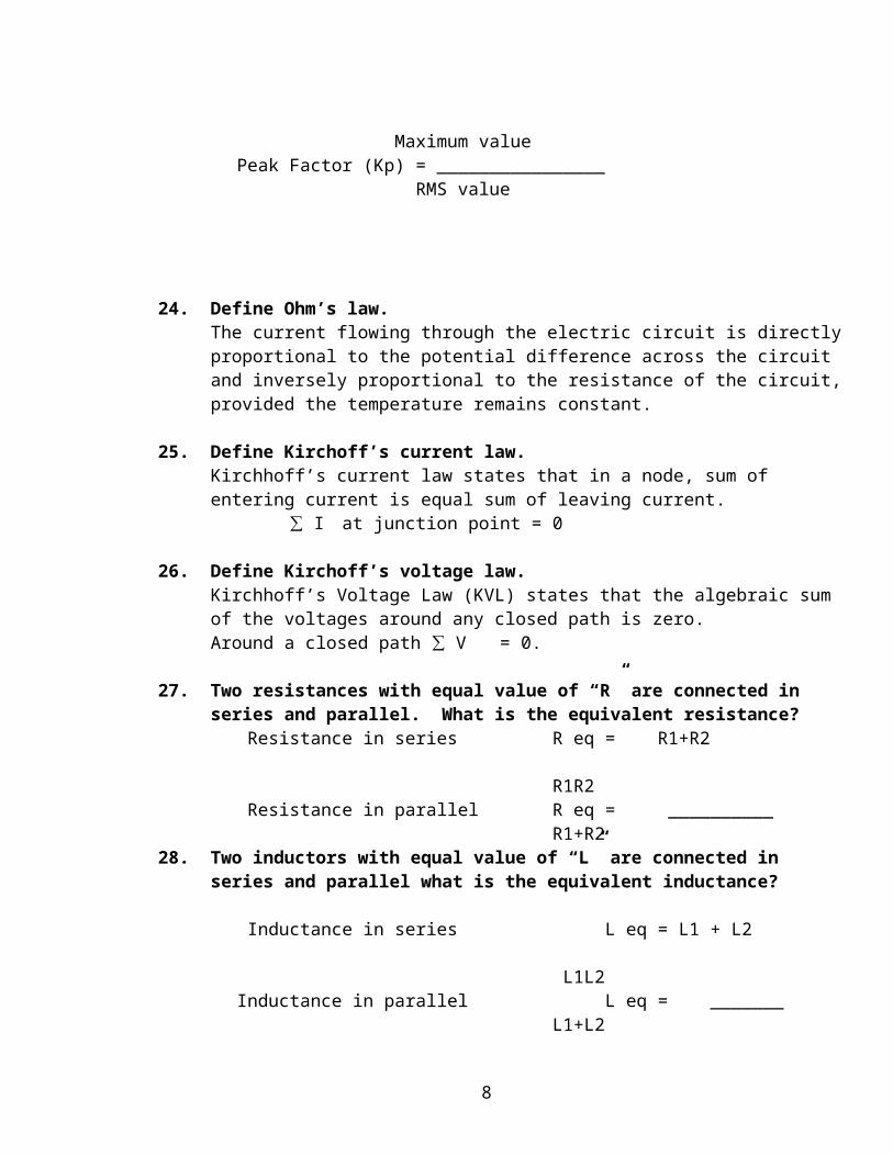
23. Define peak factor.Peak factor is defined as the ratio of the maximum value to the rms value.
Maximum valuePeak Factor (Kp) = ________________
RMS value
5
24. Define Ohm’s law.The current flowing through the electric circuit is directly proportional to the potential difference across the circuit and inversely proportional to the resistance of the circuit, provided the temperature remains constant.
25. Define Kirchoff’s current law.Kirchhoff’s current law states that in a node, sum of entering current is equal sum of leaving current.
∑ I at junction point = 0
26. Define Kirchoff’s voltage law.Kirchhoff’s Voltage Law (KVL) states that the algebraic sum of the voltages around any closed path is zero. Around a closed path ∑ V= 0.
27. Two resistances with equal value of “R” are connected in series and parallel. What is the equivalent resistance?
Resistance in series R eq = R1+R2
R1R2 Resistance in parallel R eq = __________
R1+R2 28. Two inductors with equal value of “L” are connected in series and parallel what is
the equivalent inductance?
Inductance in series L eq = L1 + L2
L1L2 Inductance in parallel L eq = _______
L1+L2
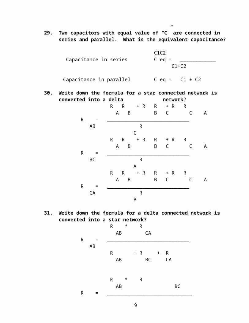
29. Two capacitors with equal value of “C” are connected in series and parallel. What is the equivalent capacitance?
C1C2 Capacitance in series C eq = ____________
C1+C2
Capacitance in parallel C eq = C1 + C2
30. Write down the formula for a star connected network is converted into a delta network?
R R + R R + R R A B B C C A
R = ____________________________ AB R
CR R + R R + R R
6

A B B C C AR = ____________________________ BC R
AR R + R R + R R A B B C C A
R = ____________________________ CA R
B
31. Write down the formula for a delta connected network is converted into a star network?
R * R AB CA
R = ____________________________ AB
R + R + R AB BC CA
R * R AB BC
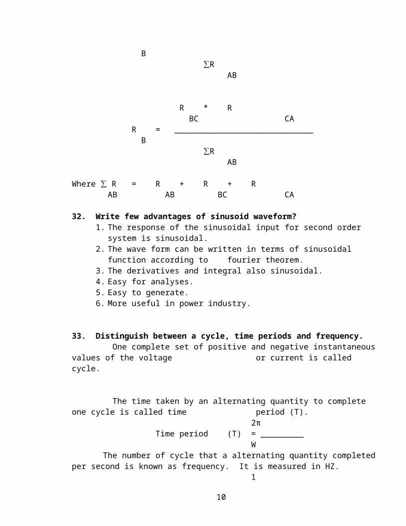
R = _____________________________ B
∑R AB
R * R BC CA
R = _____________________________ B
∑R AB
Where ∑ R = R + R + RAB AB BC CA
32. Write few advantages of sinusoid waveform?1. The response of the sinusoidal input for second order system is sinusoidal.2. The wave form can be written in terms of sinusoidal function according to fourier
theorem.3. The derivatives and integral also sinusoidal.4. Easy for analyses.5. Easy to generate.6. More useful in power industry.
7
33. Distinguish between a cycle, time periods and frequency. One complete set of positive and negative instantaneous values of the voltage
or current is called cycle.
The time taken by an alternating quantity to complete one cycle is called time period (T).
2πTime period (T) = _________
W The number of cycle that a alternating quantity completed per second is known as
frequency. It is measured in HZ.1
Frequency (f) = ________T
34. What is instantaneous value? The value of an alternating current, at any particular moment is called its
instantaneous value.
35. What are peak value and peak to peak value? The peak value of the sine wave during positive or negative half only. The sum of positive and negative value is called a peak to peak value. The
peak to peak value of a sinusoidal alternating voltage is equal to two times the peak value.
36. What is average value? The average value of the sine wave is the total area under the half-cycle curve
divided by the distance of the curve. 1 T
V = ___ ∫ V (t) dt av T 0
37. Define effective value or RMS value of a sinusoidal voltage. The R.M.S value may be determined by taking the mean of the squares of the Instantaneous value of current over one complete cycle. This is often known
as the effective value.V = ____________ rms √ 1/T T 2
∫ [V (t) dt 0
38. Define phasor. Graphical representation of phasors V = Vm <φ and I=I < - θ known phasor.
39. Define phase angle. The angle between voltage and current is called phase angle. It is denoted by φ.
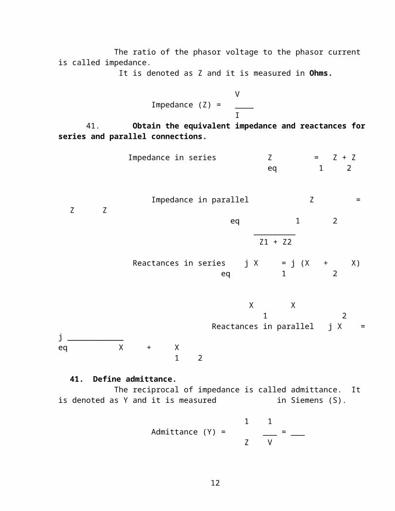
40. What is impedance? The ratio of the phasor voltage to the phasor current is called impedance.
8
It is denoted as Z and it is measured in Ohms.
VImpedance (Z) = ____
I 41. Obtain the equivalent impedance and reactances for series and parallel connections.
Impedance in series Z = Z + Z eq 1 2
Impedance in parallel Z = Z Z eq 1 2
_________ Z1 + Z2
Reactances in series j X = j (X + X)
eq 1 2
X X 1 2 Reactances in parallel j X = j ____________ eq X + X
1 2
41. Define admittance. The reciprocal of impedance is called admittance. It is denoted as Y and it is measured in Siemens (S).
1 1Admittance (Y) = ___ = ___
Z V
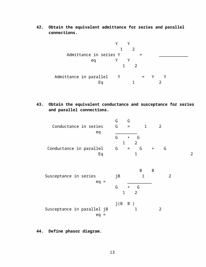
42. Obtain the equivalent admittance for series and parallel connections.
Y Y 1 2
Admittance in series Y = ____________eq Y Y
1 2
Admittance in parallel Y = Y Y Eq 1 2
9
43. Obtain the equivalent conductance and susceptance for series and parallel connections.
G G Conductance in series G = 1 2
eq _________G + G 1 2
Conductance in parallel G = G + G Eq 1 2
B B Susceptance in series jB 1 2
eq = __________G + G 1 2
j(B B )
Susceptance in parallel jB 1 2 eq =
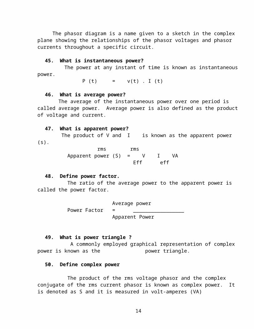
44. Define phasor diagram.The phasor diagram is a name given to a sketch in the complex plane showing the
relationships of the phasor voltages and phasor currents throughout a specific circuit.
45. What is instantaneous power? The power at any instant of time is known as instantaneous power.
P (t) = v(t) . I (t)
46. What is average power? The average of the instantaneous power over one period is called average power. Average
power is also defined as the product of voltage and current.
47. What is apparent power? The product of V and I is known as the apparent power (s).
rms rmsApparent power (S) = V I VA
Eff eff
48. Define power factor. The ratio of the average power to the apparent power is called the power factor.
Average powerPower Factor = _________________
Apparent Power
10

49. What is power triangle ? A commonly employed graphical representation of complex power is known as the power triangle.
50. Define complex power
The product of the rms voltage phasor and the complex conjugate of the rms current phasor is known as complex power. It is denoted as S and it is measured in volt-amperes (VA)
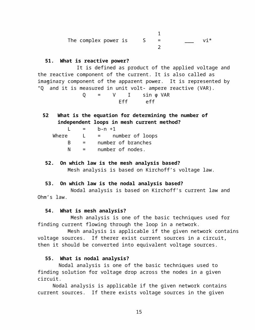
1The complex power is S = ___ vi*
2
51. What is reactive power? It is defined as product of the applied voltage and the reactive component of the current.
It is also called as imaginary component of the apparent power. It is represented by “Q” and it is measured in unit volt- ampere reactive (VAR).
Q = V I sin φ VAR Eff eff
52 What is the equation for determining the number of independent loops in mesh current method?
L = b-n +1Where L = number of loops
B = number of branchesN = number of nodes.
52. On which law is the mesh analysis based?Mesh analysis is based on Kirchoff’s voltage law.
53. On which law is the nodal analysis based? Nodal analysis is based on Kirchoff’s current law and Ohm’s law.
54. What is mesh analysis? Mesh analysis is one of the basic techniques used for finding current flowing through the
loop in a network. Mesh analysis is applicable if the given network contains voltage sources. If therer exist
current sources in a circuit, then it should be converted into equivalent voltage sources.
55. What is nodal analysis? Nodal analysis is one of the basic techniques used to finding solution for voltage drop
across the nodes in a given circuit.Nodal analysis is applicable if the given network contains current sources. If there exists
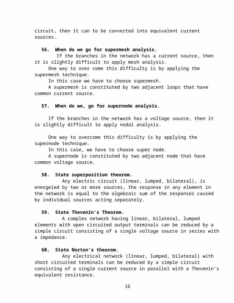
voltage sources in the given circuit, then it can to be converted into equivalent current sources.
56. When do we go for supermesh analysis. If the branches in the network has a current source, then it is slightly difficult to apply mesh
analysis.
11
One way to over come this difficulty is by applying the supermesh technique.In this case we have to choose supermesh.A supermesh is constituted by two adjacent loops that have common current source.
57. When do we, go for supernode analysis.
If the branches in the network has a voltage source, then it is slightly difficult to apply nodal analysis.
One way to overcome this difficulty is by applying the supernode technique.In this case, we have to choose super node.A supernode is constituted by two adjacent node that have common voltage source.
58. State superposition theorem.Any electric circuit (linear, lumped, bilateral), is energeied by two or more sources,
the response in any element in the network is equal to the algebraic sum of the responses caused by individual sources acting separately.
59. State Thevenin’s Theorem.A complex network having linear, bilateral, lumped elements with open circuited
output terminals can be reduced by a simple circuit consisting of a single voltage source in series with a impedance.
60. State Norton’s theorem.Any electrical network (linear, lumped, bilateral) with short circuited terminals can be
reduced by a simple circuit consisting of a single current source in parallel with a Thevenin’s equivalent resistance.
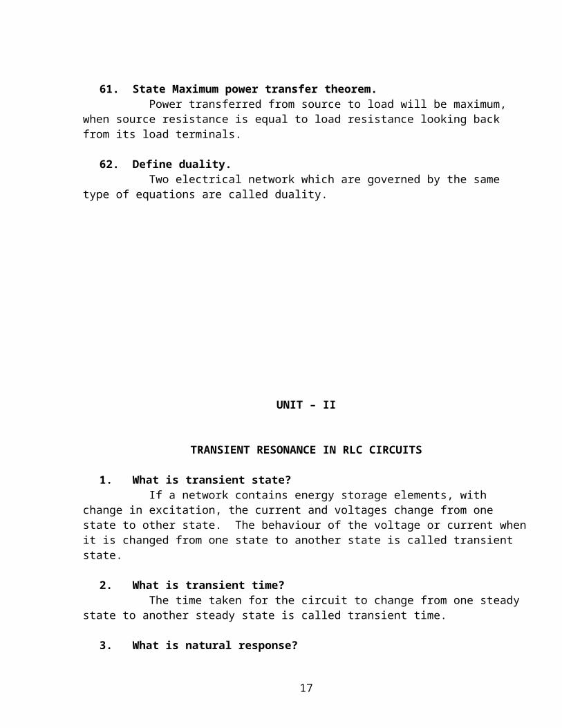
61. State Maximum power transfer theorem.Power transferred from source to load will be maximum, when source resistance is
equal to load resistance looking back from its load terminals.
62. Define duality.Two electrical network which are governed by the same type of equations are called
duality.
12
UNIT – II
TRANSIENT RESONANCE IN RLC CIRCUITS
1. What is transient state?If a network contains energy storage elements, with change in excitation, the current
and voltages change from one state to other state. The behaviour of the voltage or current when it is changed from one state to another state is called transient state.
2. What is transient time?The time taken for the circuit to change from one steady state to another steady state
is called transient time.
3. What is natural response?If we consider a circuit containing storage elements which are independent of
sources, the response depends upon the nature of the circuit, it is called natural response.
4. What is transient response?The storage elements deliver their energy to the resistances, hence the response
changes with time, gets saturated after sometime, and is referred to the transient response.
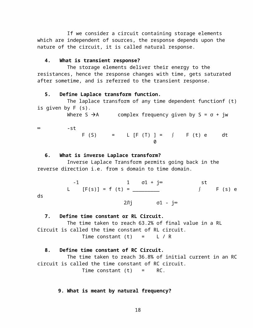
5. Define Laplace transform function.The laplace transform of any time dependent functionf (t) is given by F (s).Where S A complex frequency given by S = σ + jw ∞ -st
F (S) = L [F (T) ] = ∫ F (t) e dt 0
6. What is inverse Laplace transform?Inverse Laplace Transform permits going back in the reverse direction i.e. from s
domain to time domain.
-1 1 σ1 + j∞ stL [F(s)] = f (t) = _________ ∫ F (s) e ds
2Лj σ1 - j∞
7. Define time constant or RL Circuit.The time taken to reach 63.2% of final value in a RL Circuit is called the time
constant of RL circuit.Time constant (t) = L / R
8. Define time constant of RC Circuit.The time taken to reach 36.8% of initial current in an RC circuit is called the time
constant of RC circuit.Time constant (t) = RC.
13
9. What is meant by natural frequency?If the damping is made zero then the response oscillates with natural frequency without any
opposition, such a frequency is called natural frequency of oscillations, denoted as ώ n.
10. Define damping ratio.It is the ratio of actual resistance (R) in the circuit to the critical resistance (R cr). It is
denoted by greek letter Zeta (ξ). R R
Ξ = ____ = _____ √ C / LR cr 2
11. Define initial value theorem.The initial value theorem states that if f (t) and f’ (t) both are laplace transformable,
ThenLim f (t) = lim s F (s)T 0 s ∞
12. Define final value theorem.The final value theorem states that, if f (t) and f ‘ (t) both are laplace transformable,
thenLim f (t) = lim s F (s)T ∞ s 0
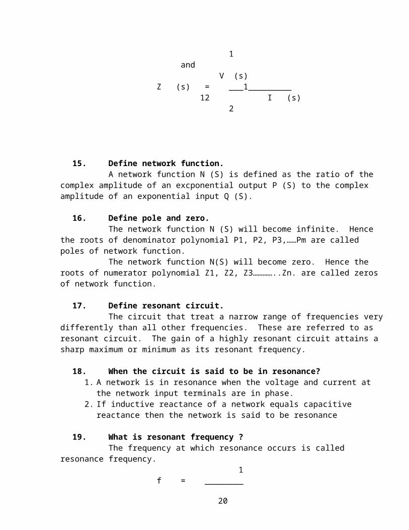
13. What is driving point impedence ?The ratio of the Laplace transform of the voltage at the point to the laplace transform of the
current at the same port is called driving point impedance.The driving point impedance of the network is define as
V(s)Z (S) = _____________
I (s)
14. What is transfer point impedance? It is defined as the ratio of voltage transform at one port to the current transform at the
other port. It is defined by V (s)
Z (s) = ___2_________ 21 I (s)
1and
V (s)Z (s) = ___1_________
12 I (s) 2
14
15. Define network function.A network function N (S) is defined as the ratio of the complex amplitude of an
excponential output P (S) to the complex amplitude of an exponential input Q (S).
16. Define pole and zero.The network function N (S) will become infinite. Hence the roots of denominator
polynomial P1, P2, P3,……Pm are called poles of network function.The network function N(S) will become zero. Hence the roots of numerator
polynomial Z1, Z2, Z3…………..Zn. are called zeros of network function.
17. Define resonant circuit.The circuit that treat a narrow range of frequencies very differently than all other
frequencies. These are referred to as resonant circuit. The gain of a highly resonant circuit attains a sharp maximum or minimum as its resonant frequency.
18. When the circuit is said to be in resonance?1. A network is in resonance when the voltage and current at the network input terminals
are in phase.2. If inductive reactance of a network equals capacitive reactance then the network is said to
be resonance
19. What is resonant frequency ?The frequency at which resonance occurs is called resonance frequency.
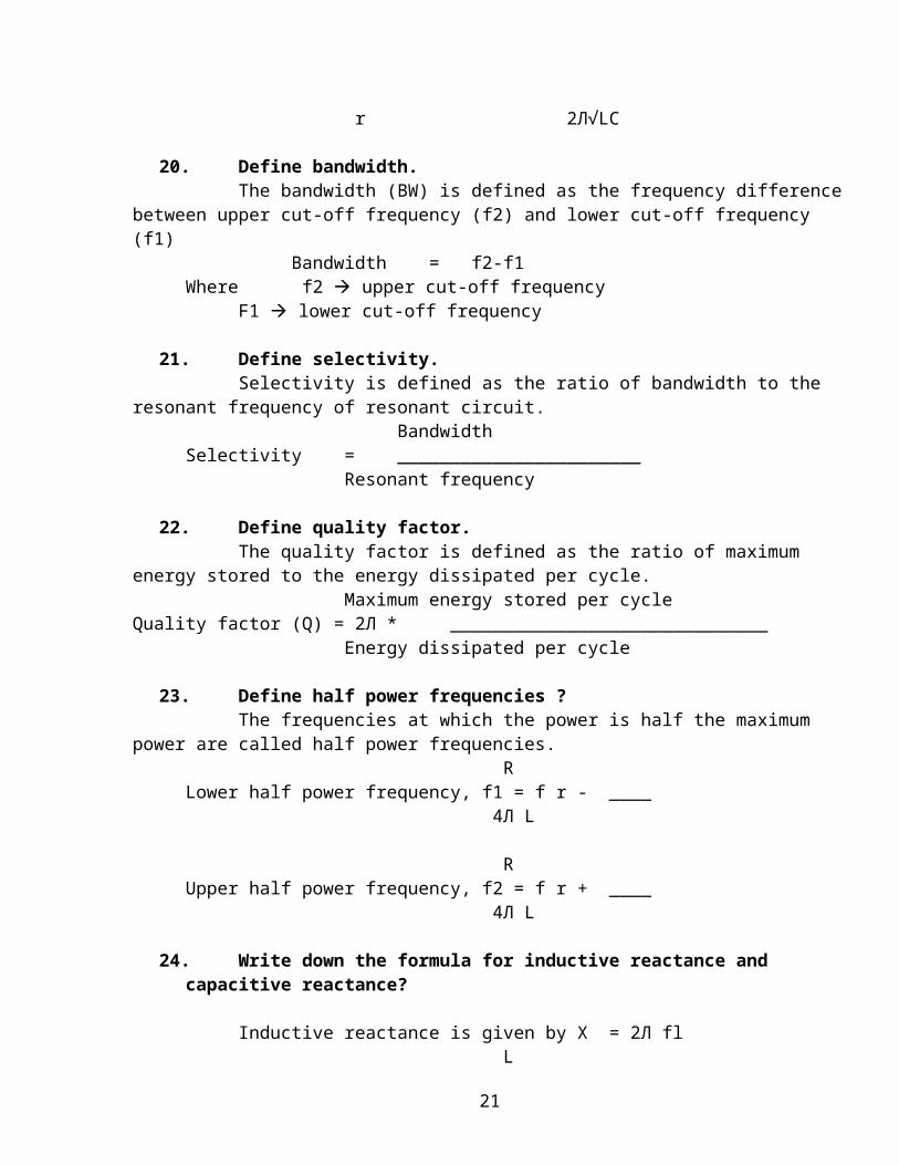
1f = ________ r 2Л√LC
20. Define bandwidth.The bandwidth (BW) is defined as the frequency difference between upper cut-off
frequency (f2) and lower cut-off frequency (f1)Bandwidth = f2-f1
Where f2 upper cut-off frequencyF1 lower cut-off frequency
21. Define selectivity.Selectivity is defined as the ratio of bandwidth to the resonant frequency of resonant
circuit.Bandwidth
Selectivity = _______________________Resonant frequency
22. Define quality factor.The quality factor is defined as the ratio of maximum energy stored to the energy
dissipated per cycle.Maximum energy stored per cycle
Quality factor (Q) = 2Л * ______________________________Energy dissipated per cycle
15
23. Define half power frequencies ?The frequencies at which the power is half the maximum power are called half power
frequencies. R
Lower half power frequency, f1 = f r - ____ 4Л L
RUpper half power frequency, f2 = f r + ____
4Л L
24. Write down the formula for inductive reactance and capacitive reactance?
Inductive reactance is given by X = 2Л fl L
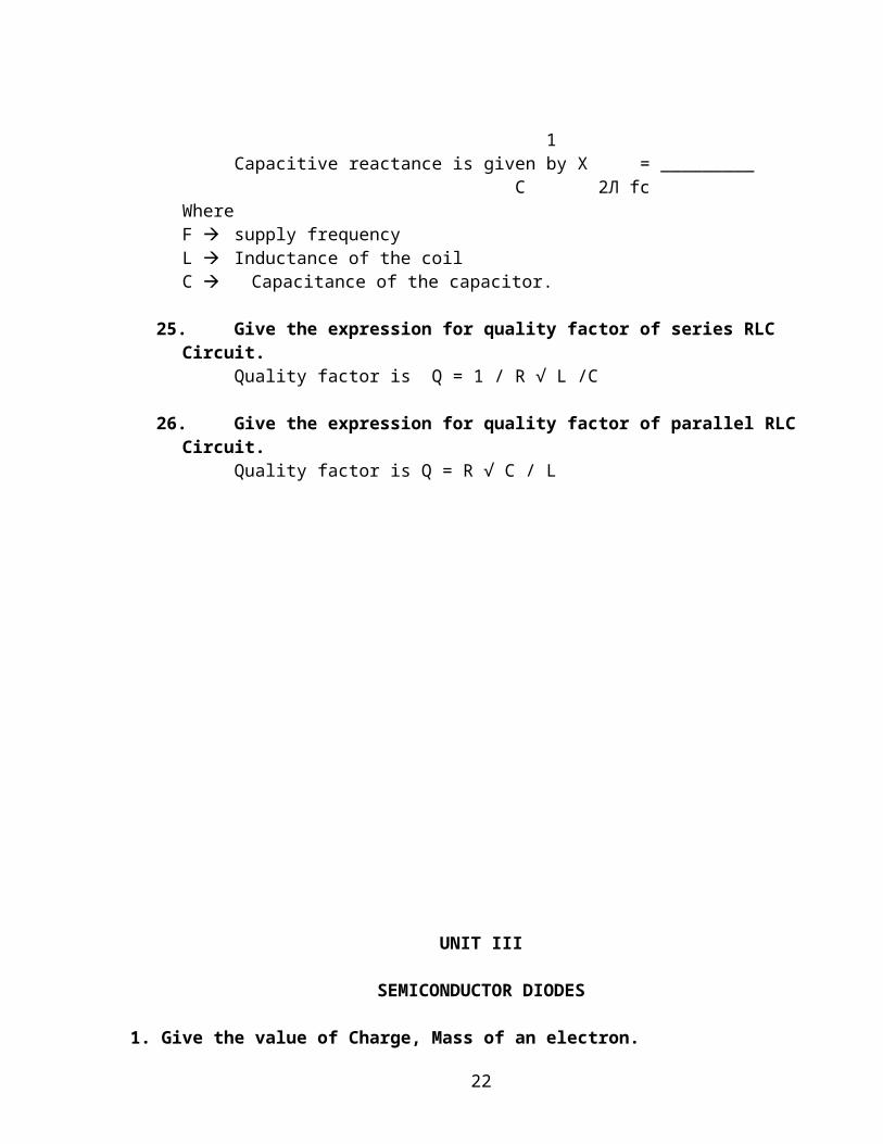
1Capacitive reactance is given by X = _________
C 2Л fcWhereF supply frequencyL Inductance of the coilC Capacitance of the capacitor.
25. Give the expression for quality factor of series RLC Circuit.Quality factor is Q = 1 / R √ L /C
26. Give the expression for quality factor of parallel RLC Circuit.Quality factor is Q = R √ C / L
16
UNIT III
SEMICONDUCTOR DIODES
1. Give the value of Charge, Mass of an electron.Charge of an electron – 1.6 x 10 -19 coloumbs & Mass of an electron - 9.11 x 10 -31 Kgs2. Define Potential.A potential of V volts at point B with respect to point A, is defined as the workdone in taking unit positive charge from A to B , against the electric field.3. Define Current density.It is defined as the current per unit area of the conducting medium. J = I / A4. Define Electron volts.If an electron falls through a potential of one volt then its energy is 1 electron volt.1 eV = 1.6 x 10 -19 joules5. What is Electrostatic deflection sensitivity?Electrostatic deflection sensitivity of a pair of deflecting plates of a cathode rayoscilloscope ( CRO) is defined as the amount of deflection of electron spotproduced when a voltage of 1 Volt DC is applied between the corresponding plates.6. What is the relation for the maximum number of electrons in each shell?Ans: 2n27. What are valence electrons?Electron in the outermost shell of an atom is called valence electron.8. What is forbidden energy gap?The space between the valence and conduction band is said to be forbidden energy gap.9. What are conductors? Give examples?Conductors are materials in which the valence and conduction band overlap each other so there is a swift movement of electrons which leads to conduction. Ex. Copper, silver.10. What are insulators? Give examples?Insulators are materials in which the valence and conduction band are far awayfrom each other. So no movement of free electrons and thus no conduction.Ex glass, plastic.11. Give the energy band structure of Insulator.In Insulators there is a wide forbidden energy gap. So movement of valenceelectron from valence to conduction band is not possible.12. Give the energy band structure of Semi conductor.In Semiconductors there is a small forbidden energy gap. So movement ofvalence electron from valence to conduction band is possible if the valenceelectrons are supplied with some energy.13. Give the energy band structure of conductor.In conductors there is no forbidden energy gap, valence band and conductionand over lap each other. so there is a heavy movement of valence electrons.14. what are Semiconductors? Give examples?The materials whose electrical property lies between those of conductors andinsulators are known as Semiconductors. Ex germanium, silicon.15. What are the types of Semiconductor?1. Intrinsic semiconductor 2. Extrinsic semiconductor.16. What is Intrinsic Semiconductor?Pure form of semiconductors are said to be intrinsic semiconductor.
17
Ex: germanium, silicon.17. Define Mass – action law.Under thermal equilibrium the product of free electron concentration (n) and holeconcentration (p) is constant regardless of the individual magnitude.n.p = ni218. What is Extrinsic Semiconductor?If certain amount of impurity atom is added to intrinsic semiconductor theresulting semiconductor is Extrinsic or impure Semiconductor.19. What are the types of Extrinsic Semiconductor?1. P-type Semiconductor 2. N- Type Semiconductor.20. What is P-type Semiconductor?The Semiconductor which are obtained by introducing pentavalent impurity atom(phosphorous, antimony) are known as P-type Semiconductor.21. What is N-type Semiconductor?The Semiconductor which is obtained by introducing trivalent impurity atom (gallium, indium) are known as N-type Semiconductor.22. What is doping?Process of adding impurity to a intrinsic semiconductor atom is doping. The impurity is called dopant.23. Which charge carriers is majority and minority carrier in N-typeSemiconductor?majority carrier: electron and minority carrier: holes.24.which charge carriers is majority and minority carrier in P-typeSemiconductor?Majority carrier: holes and minority carrier: electron25. Why n - type or penta valent impurities are called as Donor impurities?n- type impurities will donate the excess negative charge carriers ( Electrons) and therefore they are reffered to as donor impurities.26. Why P – type or trivalent impurities are called as acceptor impurity?p- type impurities make available positive carriers because they create holes which can accept electron, so these impurities are said to be as acceptor impurity.27. Give the relation for concentration of holes in the n- type material?pn = ni2 /NDWherepn - concentration of holes in the n – type semiconductorND - concentration of donor atoms in the n – type semiconductor28. Give the relation for concentration of electrons in the p - type material?np = ni2 /NAWherenp - concentration of electrons in p- type semiconductorND - concentration of acceptor atoms in the p – type semiconductor29. Define drift current?When an electric field is applied across the semiconductor, the holes move towards the negative terminal of the battery and electron move towards the positive terminal of the battery. This drift movement of charge carriers will result in a current termed as drift current.
18

30. Give the expression for drift current density due to electron.Jn = q n μnEWhere,Jn - drift current density due to electronq- Charge of electronμn - Mobility of electronE - applied electric field31. Give the expression for drift current density due to holes.Jp = q p μp EWhere, Jn - drift current density due to holes q - Charge of holesμp - Mobility of holes E - applied electric field32. Define the term diffusion current?A concentration gradient exists, if the number of either electrons or holes is greater in one region of a semiconductor as compared to the rest of the region. The holes and electron tend to move from region of higher concentration to the region of lower concentration. This process in called diffusion and the current produced due this movement is diffusion current.33. Define mean life time of a hole or and electron.The electron hole pair created due to thermal agitation woll disappear as a result of recombination. Thus an average time for which a hole or an electron exist before recombination can be said as the mean life time of a hole or electron.34. What is the other name of continuity equation? What does it indicate?The other name of continuity equation is equation of conservation of charge.This equation indicates that the rate at which holes are generated thermally just equals the rate at which holes are lost because of recombination under equilibrium conditions.35. Define Hall effect?If a metal or semiconductor carrying current I is placed in a transverse magnetic field B , an electric field E is induced in the direction perpendicular to both I and B This phenomenon is known as Hall effect.36. Give some application of Hall Effect.i). Hall Effect can be used to measure the strength of a magnetic field in terms of electrical voltage.ii).It is used to determine whether the semiconductor is p – type or n- type materialiii).It is used to determine the carrier concentrationiv).It is used to determine the mobility.37. Define the term transition capacitance?When a PN junction is reverse biased, the depletion layer acts like a dielectric material while P and N –type regions on either side which has low resistance act as the plates. In this way a reverse biased PN junction may be regarded as parallel plate capacitor and thus the capacitance across this set up is called as the transition capacitance.CT = A / WWhereCT - transition capacitanceA - Cross section area of the junctionW – Width of the depletion region38. What is a varactor diode?A diode which is based on the voltage variable capacitance of the reverse biased p-n junction is said to be varactor diode. It has other names such as varicaps, voltacaps.
19
39. Define the term diffusion capacitance.The diffusion capacitance of a forward biased diode is defined as the rate of change of injected charge with voltage.CD = I / VTWhere, Cd – time constant I – current across the diode vT – threshold voltage40. what is recovery time? Give its types.When a diode has its state changed from one type of bias to other a transient accompanies the diode response, i.e., the diode reaches steady state only after an interval of time “ tr” called as recovery time. The recovery time can be divided in to two types such as(i) forward recovery time(ii) reverse recovery time
20
41. What is meant by forward recovery time?The forward recovery time may be defined as the time interval from the instant of 10% diode voltage to the instant this voltage reaches 90% of the final value. It is represented as t f r.
42. What is meant by reverse recovery time?The reverse recovery time can be defined as the time required for injected or the excess minority carrier density reduced to zero , when external voltage is suddenly reversed.
43. Define storage time.The interval time for the stored minority charge to become zero is called storage time. It is represented as t s.
44. Define transition time.The time when the diode has normally recovered and the diode reverse current reaches reverse saturaton current I0 is called as transition time. It is represented as t t
45. What are break down diodes?Diodes which are designed with adequate power dissipation capabilities to operate in the break down region are called as break down or zener diodes.
46. What is break down? What are its types?When the reverse voltage across the pn junction is increased rapidly at a voltage the junction breaks down leading to a current flow across the device. This phenomenon is called as break down and the voltage is break down voltage. The types of break down arei) zener break downii)Avalanche breakdown
47. What is zener breakdown?Zener break down takes place when both sides of the junction are very heavily doped and Consequently the depletion layer is thin and consequently the depletion layer is tin. When a small value of reverse bias voltage is applied , a very strong electric field is set up across the thin depletion layer. This electric field is enough to break the covalent bonds. Now extremely large number of freecharge carriers are produced which constitute the zener current. This process is known as zener break down.
48. What is avalanche break down?When bias is applied , thermally generated carriers which are already present in the diode acquire sufficient energy from the applied potential to produce new carriers by removing valence electron from their bonds. These newly generated additional carriers acquire more energy from the potential and they strike the lattice and create more number of free electrons and holes. This process goeson as long as bias is increased and the number of free carriers get multiplied. This process is termed as avalanche multiplication. Thus the break down which occur in the junction resulting in heavy flow of current is termed as avalanche break down.
21
49. How does the avalanche breakdown voltage vary with temperature?In lightly doped diode an increase in temperature increases the probability of collision of electrons and thus increases the depletion width. Thus the electrons and holes needs a high voltage to cross the junction. Thus the avalanche voltage is increased with increased temperature.50. How does the zener breakdown voltage vary with temperature?In heavily doped diodes, an increase in temperature increases the energies of valence electrons, and hence makes it easier for these electrons to escape from covalent bonds. Thus less voltage is
22
sufficient to knock or pull these electrons from their position in the crystal and convert them in to conduction electrons. Thus zener break down voltage decreases with temperature.
UNIT IV
TRANSISTORS51. What is a transistor (BJT)?Transistor is a three terminal device whose output current, voltage and /or poweris controlled by input current.52. What are the terminals present in a transistor?Three terminals: emitter, base, collector.53. What is FET?FET is abbreviated for field effect transistor. It is a three terminal device with its output characteristics controlled by input voltage.54. Why FET is called voltage controlled device?The output characteristics of FET is controlled by its input voltage thus it is voltage controlled.55. What are the two main types of FET?1. JFET 2. MOSFET.56. What are the terminals available in FET?1). Drain, 2).Source and 3). Gate57. What is JFET?JFET- Junction Field Effect Transistor.58. What are the types of JFET?N- Channel JFET and P- Channel JFET59. What are the two important characteristics of JFET?1. Drain characteristics 2. Transfer characteristics.60. What is transconductance in JFET?It is the ratio of small change in drain current to the corresponding change in drain to source voltage.61. What is amplification factor in JFET?It is the ratio of small change in drain to source voltage to the corresponding change in Gate to source voltage.62. Why do we choose q point at the center of the loadline?The operating point of a transistor is kept fixed usually at the center of the active region in order that the input signal is well amplified. If the point is fixed in the saturation region or the cut off region the positive and negative half cycle gets clipped off respectively.63. List out the different types of biasing. ._Voltage divider bias, Base bias, Emitter feed back bias, Collector feedback bias, Emitter bias.
64. What do you meant by thermal runway?Due to the self heating at the collector junction, the collector current rises. This causes damage to the device. This phenomenon is called thermal runway.65. Why is the transistor called a current controlled device?The output characteristics of the transistor depend on the input current. So thtransistor is called a current controlled device.66. Define current amplification factor?
23

It is defined as the ratio of change in output current to the change in input current at constant.67. What are the requirements for biasing circuits?• The q point must be taken at the Centre of the active region of the output characteristics.• Stabilize the collector current against the temperature variations.• Make the q point independent of the transistor parameters.• When the transistor is replaced, it must be of same type.68. When does a transistor act as a switch?The transistor acts as a switch when it is operated at either cutoff region or saturation region69. What is biasing?To use the transistor in any application it is necessary to provide sufficient voltage and current to operate the transistor. This is called biasing.70. What is stability factor?Stability factor is defined as the rate of change of collector current with respect to the rate of change of reverse saturation current.71. Explain about the various regions in a transistor?The three regions are active region saturation region cutoff region.72. Explain about the characteristics of a transistor?Input characteristics: it is drawn between input voltage & input current while keeping output voltage as constant. Output characteristics: It is drawn between the output voltage &output current while keeping input current as constant.
16 marks-Hints73. Explain the construction, operation, volt ampere characteristics, and applicationof SCR, also explain its two transistor model.Maximum mark for this question: 16 marksConstruction (2marks)Equivalent circuit and two transistor model (2marks)Operation (4marks)Volt ampere characteristics (4marks)Application (2marks)74. Explain the construction, operation, equivalent circuit, volt amperecharacteristics, and application of UJT.Maximum mark for this question: 16 marksConstruction (4marks)Equivalent circuit (2marks)Operation (4marks)Volt ampere characteristics (4marks)Application (2marks)75. Explain the construction, operation, equivalent circuit, volt amperecharacteristics, and application of DIAC.Maximum mark for this question: 16 marksConstruction (4marks)Equivalent circuit (2marks)Operation (4marks)Volt ampere characteristics (4marks)Application (2marks)76. Explain the construction, operation, equivalent circuit, volt amperecharacteristics, and application of TRIACMaximum mark for this question: 16 marks
24
Construction (4marks)Equivalent circuit (2marks)Operation (4marks)Volt ampere characteristics (4marks)Application (2marks)
UNIT V
SPECIAL SEMICONDUCTOR DEVICES
78. What is a TRIAC?TRIAC is a three terminal bidirectional semiconductor switching device. It can conduct in both the directions for any desired period. In operation it is equivalent to two SCR’s connected in antiparallel.79. Give the application of TRIAC.1. Heater control2. Motor speed control3. Phase control4. Static switches80. What are the different operating modes of TRIAC?1. Keeping MT2 and G positive2. Keeping MT2 and G negative.3. Keeping MT2 positive and G negative.4. Keeping MT2 negative and G positive.81. What are the regions in the VI characteristics of UJT?1. Cut-off region2. Negative resistance region.3. Saturation region82. What is meant by negative resistance region of UJT?In a UJT when the emitter voltage reaches the peak point voltage, emitter current starts flowing. After the peak point any effort to increase in emitter voltage further leads to sudden increase in the emitter current with corresponding decrease in emitter voltage, exhibiting negative resistance. This takes place until the valley point is reached. This region between the peak point and valley point is called negative resistance region.83. Mention the applications of UJT.1. It is used in timing circuits2. It is used in switching circuits3. It is used in phase control circuits
25

4. It can be used as trigger device for SCR and triac.5. It is used in saw tooth generator.6. It is used for pulse generation.84. What is a DIAC?DIAC is a two terminal bidirectional semiconductor switching device. . It can conduct in either direction depending upon the polarity of the voltage applied across its main terminals. In operation DIAC is equivalent to two 4 layer diodes connected in antiparallel.85. Give some applications of DIAC.1. To trigger TRIAC2. Motor speed control3. Heat control4. Light dimmer circuits87. What is a SCR?A silicon controller rectifier (SCR) is a three terminal, three junction semiconductor device that acts as a true electronic switch. It is a unidirectional device. It converts alternating current into direct current and controls the amount of power fed to the load.88. Define break over voltage of SCR.Break over voltage is defined as the minimum forward voltage with gate open at which the SCR starts conducting heavily.89.Why SCR cannot be used as a bidirectional switch.SCR can do conduction only when anode is positive with respect to cathode with proper gate current. Therefore, SCR operates only in one direction and cannot be used as bidirectional switch.90. How turning on of SCR is done?1. By increasing the voltage across SCR above forward break over voltage.2. By applying a small positive voltage at gate.3. By rapidly increasing the anode to cathode voltage.4. By irradiating SCR with light.91. How turning off of SCR is done?1. By reversing the polarity of anode to cathode voltage.2. By reducing the current through the SCR below holding current.3.By interrupting anode current by means of momentarily series or parallel switching92. Define holding current in a SCR.Holding current is defined as the minimum value of anode current to keep the SCR ON.93. List the advantages of SCR.1. SCR can handle and control large currents.2. Its switching speed is very high3. It has no moving parts, therefore it gives noiseless operation.4. Its operating efficiency is high.94. List the application of SCR.1. It can be used as a speed controller in DC and AC motors.2. It can be used as an inverter.3. It can be used as a converter4. It is used in battery chargers.5. It is used for phase control and heater control.6. It is used in light dimming control circuits.95. What is meant by latching.The ability of SCR to remain conducting even when the gate signal is removed is called as latching.96. Define forward current rating of a SCR.
26

Forward current rating of a SCR is the maximum anode current that it can handle without destruction.97. List the important ratings of SCR.1. Forward break over voltage2. Holding current3. Gate trigger current4. Average forward current5. Reverse break down voltage.98. Compare SCR with TRIAC. SCR TRIAC1. unidirectional current 1. bidirectional current2. triggered by positive pulse at gate 2. triggered by pulse of positive or negative at gate3. fast turn off time 3,. Longer turn off time4. large current ratings 4. lower current ratings99. Differentiate BJT and UJT.
BJT UJT1. It has two PN junctions 1. It has only one PN junctions2. three terminals present 2. three terminals present are emitter, are emitter, base,collector base1,base23. basically a amplifying device 3. basically a switching device
100. What is Shockley diode (PNPN diode)?Shockley diode is a four layered PNPN silicon diode. It is a low- current SCR without a gate. This device is switched ON when the anode to cathode voltage is increased to forward switching voltageVS which is equivalent to SCR forward break over voltage.
101. What is a thyristor?Thyristor is a semiconductor device having three or more junctions .Such a device acts as a switch without any bias and can be fabricated to have voltage ratings of severalhundred volts and current ratings from a few amperes to almost thousand amperes.
102. What are the types of thyristors?1. Unidirectional thyristors2. Bidirectional thyristors3. Low-power thyristors103. Give the various triggering devices for thyristors.1. SCR2. UJT3. DIAC4. TRIAC104. what is backward diode?The backward diode is a diode in which the doping level is moderate. The forward current in this case is very small, very much similar to that of the reverse current in the conventional diode.105. what is a photo diode?
27

The photo diode is a diode in which the current sensitivity to radiation can be made much larger by the use of the reverse biased PN junction. Thus this diode conducts heavily in the reverse bias when there is some radiaton allowed to fall on the PN junction.106. What is a LED?A PN junction diode which emits light when forward biased is known as Light emitting diode (LED).107. What is a tunnel diode?The tunnel diode is a pn junction diode in which the impurity concentration is greatly increased about 1000 times higher than a conventional PN junction diode thus yielding a very thin depletion layer. This diode utilizes a phenomenon called tunneling and hence the diode is referred as tunnel diode.108. What is tunneling phenomenon?The phenomenon of penetration of the charge carriers directly though the potential barrier instead of climbing over it is called as tunneling.
28
Related Documents