arXiv:1005.2484v1 [cond-mat.str-el] 14 May 2010 Electron Confinement, Orbital Ordering, and Orbital Moments in d 0 -d 1 Oxide Heterostructures Victor Pardo 1,2, * and Warren E. Pickett 1, † 1 Department of Physics, University of California, Davis, CA 95616 2 Departamento de F´ ısica Aplicada, Universidade de Santiago de Compostela, E-15782 Santiago de Compostela, Spain The (SrTiO3)m/(SrVO3)n d 0 - d 1 multilayer system is studied with first principles methods through the observed insulator-to-metal transition with increasing thickness of the SrVO3 layer. When correlation effects with reasonable magnitude are included, crystal field splittings from the structural relaxations together with spin-orbit coupling (SOC) determines the behavior of the elec- tronic and magnetic structures. These confined slabs of SrVO3 prefer Q orb =(π,π) orbital ordering of ℓz = 0 and ℓz = -1(jz = - 1 2 ) orbitals within the plane, accompanied by Qspin=(0,0) spin order (ferromagnetic alignment). The result is a SOC-driven ferromagnetic Mott insulator. The orbital moment of 0.75 μB strongly compensates the spin moment on the ℓz = -1 sublattice. The insulator-metal transition for n =1 → 5 (occurring between n=4 and n=5) is reproduced. Unlike in the isoelectronic d 0 - d 1 TiO2/VO2 (rutile structure) system and in spite of some similarities in orbital ordering, no semi-Dirac point [Phys. Rev. Lett. 102, 166803 (2009)] is encountered, but the insulator-to-metal transition occurs through a different type of unusual phase. For n=5 this system is very near (or at) a unique semimetallic state in which the Fermi energy is topologically determined and the Fermi surface consists of identical electron and hole Fermi circles centered at k=0. The dispersion consists of what can be regarded as a continuum of radially-directed Dirac points, forming a “Dirac circle”. I. BACKGROUND Oxide heterostructures with a polar discontinuity across interfaces have attracted a great deal of atten- tion recently, due to the unusual electronic behavior that can arise. 1,2 It is now becoming evident that heterostructures with non-polar interfaces can also lead to unanticipated behavior, including low en- ergy dispersion that is distinct from any previously known system. The specific example is the d 0 /d 1 interface system TiO 2 /VO 2 that displays a point Fermi surface, from which semi-Dirac dispersion 3 emerges. Semi-Dirac dispersion is characterized by conventional, massive dispersion along one direction in the two-dimensional plane but massless dispersion in the perpendicular direction. Although reminiscent of graphene, the semi- Dirac system displays its own distinctive low en- ergy properties. 4 The behavior is actually an elec- tron confinement phenomenon assisted by a partic- ular orbital ordering, and these nanostructures dis- play a peculiar metal-insulator transition 5 as the thickness of the d 1 oxide is increased. In these rutile structured oxides, the metal-insulator transi- tion takes place through an intermediate semi-Dirac point when the thickness is approximately 1 nm, where the system is neither insulating nor conduct- ing and the Fermi surface is point-like. Transition metal oxide perovskites with 3d 1 con- figuration are known to be on the borderline between metallic and insulating, depending on the relative sizes of several electronic energy scales, including the ratio between the on-site Coulomb repulsion U and the bandwidth W of the d electrons, and the competition between magnetic energies and Jahn- Teller splittings. For small U/W, the material will be metallic, like the correlated metal 6 SrVO 3 . For a large value of the ratio U/W, the system will present a more localized behavior, and a Mott insulator will result, as in LaTiO 3 or YTiO 3 . 7 Other energy scales may also affect, or even determine, the delicate bal- ance. Multilayers of SrVO 3 (SVO) and SrTiO 3 (STO) have been grown on STO substrates by Kim et al. and have displayed a transition 8 from the typical in- sulating behavior of STO to the metallic behavior of SVO as the number of layers of each constituent is increased. Superlattices formed by films with 2 layers of STO and 6 layers of SVO [we will denote (SrTiO 3 ) m /(SrVO 3 ) n (001) oriented multilayers as m/n] already show metallic behavior with a nearly flat resistivity curve with magnitude close to that of SVO. However, from the behavior of the resistiv- ity, it was observed that the 2/3, 2/4 and 2/6 films (increasing SVO thickness) show an insulator-metal transition at temperatures ranging from about 100 K for the 2/6 film to the approximately 230 K of the 2/4 and 2/3 films. It is to be noted also that only 2 layers of STO are not enough to isolate the SVO slabs, as can be seen from the resistivity data for the 2/3 and 3/3 systems. In fact, the 2/3 system is already semi-metallic, but four layers of STO are enough to render interactions between neighboring SVO slabs negligible. Five SVO layers are needed to obtain a metallic state, as we show below from our calculations.

Welcome message from author
This document is posted to help you gain knowledge. Please leave a comment to let me know what you think about it! Share it to your friends and learn new things together.
Transcript
arX
iv:1
005.
2484
v1 [
cond
-mat
.str
-el]
14
May
201
0
Electron Confinement, Orbital Ordering, and Orbital Moments
in d0-d1 Oxide Heterostructures
Victor Pardo1, 2, ∗ and Warren E. Pickett1, †
1Department of Physics, University of California, Davis, CA 956162 Departamento de Fısica Aplicada, Universidade de Santiago de Compostela, E-15782 Santiago de Compostela, Spain
The (SrTiO3)m/(SrVO3)n d0 − d1 multilayer system is studied with first principles methodsthrough the observed insulator-to-metal transition with increasing thickness of the SrVO3 layer.When correlation effects with reasonable magnitude are included, crystal field splittings from thestructural relaxations together with spin-orbit coupling (SOC) determines the behavior of the elec-tronic and magnetic structures. These confined slabs of SrVO3 prefer Qorb=(π, π) orbital orderingof ℓz = 0 and ℓz = −1 (jz = − 1
2) orbitals within the plane, accompanied by Qspin=(0,0) spin
order (ferromagnetic alignment). The result is a SOC-driven ferromagnetic Mott insulator. Theorbital moment of 0.75 µB strongly compensates the spin moment on the ℓz = −1 sublattice. Theinsulator-metal transition for n = 1 → 5 (occurring between n=4 and n=5) is reproduced. Unlikein the isoelectronic d0 − d1 TiO2/VO2 (rutile structure) system and in spite of some similarities inorbital ordering, no semi-Dirac point [Phys. Rev. Lett. 102, 166803 (2009)] is encountered, butthe insulator-to-metal transition occurs through a different type of unusual phase. For n=5 thissystem is very near (or at) a unique semimetallic state in which the Fermi energy is topologicallydetermined and the Fermi surface consists of identical electron and hole Fermi circles centered atk=0. The dispersion consists of what can be regarded as a continuum of radially-directed Diracpoints, forming a “Dirac circle”.
I. BACKGROUND
Oxide heterostructures with a polar discontinuityacross interfaces have attracted a great deal of atten-tion recently, due to the unusual electronic behaviorthat can arise.1,2 It is now becoming evident thatheterostructures with non-polar interfaces can alsolead to unanticipated behavior, including low en-ergy dispersion that is distinct from any previouslyknown system. The specific example is the d0/d1
interface system TiO2/VO2 that displays a pointFermi surface, from which semi-Dirac dispersion3
emerges. Semi-Dirac dispersion is characterized byconventional, massive dispersion along one directionin the two-dimensional plane but massless dispersionin the perpendicular direction.
Although reminiscent of graphene, the semi-Dirac system displays its own distinctive low en-ergy properties.4 The behavior is actually an elec-tron confinement phenomenon assisted by a partic-ular orbital ordering, and these nanostructures dis-play a peculiar metal-insulator transition5 as thethickness of the d1 oxide is increased. In theserutile structured oxides, the metal-insulator transi-tion takes place through an intermediate semi-Diracpoint when the thickness is approximately 1 nm,where the system is neither insulating nor conduct-ing and the Fermi surface is point-like.
Transition metal oxide perovskites with 3d1 con-figuration are known to be on the borderline betweenmetallic and insulating, depending on the relativesizes of several electronic energy scales, includingthe ratio between the on-site Coulomb repulsion U
and the bandwidth W of the d electrons, and thecompetition between magnetic energies and Jahn-Teller splittings. For small U/W, the material willbe metallic, like the correlated metal6 SrVO3. For alarge value of the ratio U/W, the system will presenta more localized behavior, and a Mott insulator willresult, as in LaTiO3 or YTiO3.
7 Other energy scalesmay also affect, or even determine, the delicate bal-ance.
Multilayers of SrVO3 (SVO) and SrTiO3 (STO)have been grown on STO substrates by Kim et al.
and have displayed a transition8 from the typical in-sulating behavior of STO to the metallic behaviorof SVO as the number of layers of each constituentis increased. Superlattices formed by films with 2layers of STO and 6 layers of SVO [we will denote(SrTiO3)m/(SrVO3)n (001) oriented multilayers asm/n] already show metallic behavior with a nearlyflat resistivity curve with magnitude close to thatof SVO. However, from the behavior of the resistiv-ity, it was observed that the 2/3, 2/4 and 2/6 films(increasing SVO thickness) show an insulator-metaltransition at temperatures ranging from about 100K for the 2/6 film to the approximately 230 K ofthe 2/4 and 2/3 films. It is to be noted also thatonly 2 layers of STO are not enough to isolate theSVO slabs, as can be seen from the resistivity datafor the 2/3 and 3/3 systems. In fact, the 2/3 systemis already semi-metallic, but four layers of STO areenough to render interactions between neighboringSVO slabs negligible. Five SVO layers are needed toobtain a metallic state, as we show below from ourcalculations.
In this paper we extend our investigations of d0-d1
nanostructures by studying this STO/SVO system,focusing on the differences that the crystal structure,with its specific crystal field splittings, can cause.We choose the most commonly studied structure,perovskite, with the previously studied nanostruc-tures with rutile crystal structure. We will comparedifferent orbital orderings and magnetic arrange-ments, and also study how the insulator to metaltransition occurs with increasing thickness of the d1
material (SrVO3).
II. COMPUTATIONAL METHODS
Our electronic structure calculations were per-formed within density functional theory9 using theall-electron, full potential code wien2k
10 basedon the augmented plane wave plus local orbital(APW+lo) basis set11. The exchange-correlationpotential utilized for the structure optimizations wasthe generalized gradient approximation (GGA) inthe Perdew-Burke-Ernzerhof (PBE)12. To deal withstrong correlation effects that are evident in SrVO3
we apply the LSDA+U scheme13,14 including an on-site U and J (on-site Coulomb repulsion and ex-change strengths) for the Ti and V 3d states. Thevalues U= 4.5 eV, J= 0.7 eV have been used for V todeal properly with correlations in this multilayeredstructure; these values are comparable to those usedin literature for d1 systems15–17. Our calculationsshow that a larger U, above 5.0 eV, give an incorrectinsulating behavior of bulk SrVO3 in cubic struc-ture, hence overestimating electron-electron interac-tions. Since Ti d states never have any significantoccupation, including U or not on Ti 3d orbitals hasnegligible consequence. Spin-orbit coupling (SOC)effects on the valence and conduction states, whichis discussed in the last section, have been introducedin a second variational procedure built on the scalarrelativistic approximation.
III. TREATING CORRELATION EFFECTS
IN BULK SRVO3
We have first performed calculations on bulkSrVO3 (SVO) to establish the thick SrVO3 limitof these nanostructures. Experimentally, SrVO3 isa ferromagnetic (FM) metal18 crystallizing in a cu-bic perovskite structure.19 No distortion from cubicstructure has been observed experimentally, which isconsistent to its metallic character; a Mott insulat-ing d1 system would be expected to distort due to or-bital ordering. Our calculations show that the moststable structure based on GGA exchange-correlation
(not including on-site Coulomb repulsion effects) iscubic with no distortions. However, a non-magneticsolution is obtained as a ground state within GGA.When correlations are introduced by means of
the LDA+U method, the most stable structure isslightly distorted. This broken symmetry arises be-cause the LDA+U method tends to promote integeroccupations of one of the t2g orbitals (which becomeslower in energy, and preferentially occupied).Calculations were carried out with a tetragonal
distortion in bulk SrVO3 and with various values ofthe on-site Coulomb repulsion U. LDA+U calcula-tions predict two possible orbital configurations: aFM configuration with all the t2g bands equally oc-cupied and an AF solution with a substantial occu-pation of the dxy orbital. As U increases above 5 eV,the AF solution is more stable, even for undistortedcubic perovskite, leading to an incorrect AF insulat-ing state. In all ranges of U studied (3 to 7 eV), atetragonal distortion is more stable, whereas a sim-ple GGA calculation leads to an undistorted cubicsolution, in agreement with experiment. Even in thecase of a FM solution, when a U is introduced in thecalculations, a tetragonal distortion is obtained asa ground state, in disagreement with experimentalobservations. Using the correct structure obtainedfrom both experiment and GGA calculations (whichagree), the LDA+U method with values of U smallerthan 5 eV leads to the correct FM metallic state asground state.Within GGA (U = 0) SVO is a cubic metal, with
all the t2g orbitals are equally occupied. WithinLDA+U, a tetragonal distortion causes the prefer-ential occupation of the dxy orbital, an insulatingstate and also an antiferromagnetic (AFM) orderingto be stabilized, whereas a cubic FM metallic state isobserved experimentally. This is the case also whenLDA+U is applied for the structure relaxed withGGA. For this reason, throughout the paper, we willuse for structure optimizations of these multilayersincluding such a moderately correlated compound,the GGA-PBE functional.12 With the structure thusdetermined, we use the LDA+U method for the cal-culations of the electronic and magnetic structure,and energy differences. In bulk SVO this procedureproperly results in a FM half metal with 1 µB/Vatom.
IV. GENERAL CONSIDERATIONS
SrVO3 has a lattice parameter of 3.84 A,19 whilethe lattice parameter of SrTiO3 (STO) is 3.90 A.20
Since most of these superlattices are grown on aSrTiO3 substrate, for closest comparison with exper-imental data we fix the a lattice parameter to be the
2
STO lattice parameter. However, we use the GGA-PBE exchange-correlation potential to optimize thesuperlattice c parameter and also the internal co-ordinates of all the atoms by a force minimizationtogether with a total energy minimization.Since the IF between SVO and STO has no polar
discontinuity, the distortions introduced at the inter-face between the two oxides by the nanostructuringcan be understood as first, strain due to the latticeparameter mismatch (1.5%), and secondly, to chargeimbalance within the V t2g orbitals. However, noionic charge compensation effects of the sort thatare so interesting in LaAlO3/SrTiO3 nanostructuresare present.1,21–26
We compare results for m/n multilayers with m=4 layers of STO (about 1.6 nm thickness) sandwich-ing an SVO layer with variable thickness from 1 to 5layers of SVO (0.4 to 2.0 nm), because we find 4 lay-ers of STO sufficient to isolate the SVO slabs to givetwo-dimensional behavior (negligible kz-dispersionin the band structure). We analyze the evolutionof the electronic structure for increasing thickness ofSVO slabs (n from 1 to 5).
A. d1 V ion in an octahedral environment
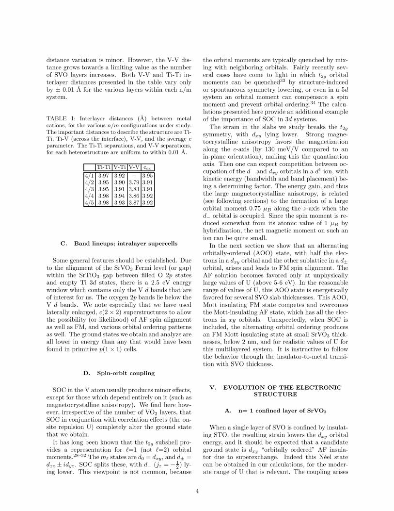
FIG. 1: (Color online) Spin density isosurface of the n=2system at 0.8 e/A3. Shown is a top view of the x − yplane in the planar AF Mott insulator state, which isthe most stable only at larger values of U. The dxy or-bital is occupied on each V ion. Different colors indicatedifferent spin directions.
One common feature within the SVO sublayer for
all thicknesses we have studied is that the V octa-hedral environment, especially at the interface (IF),will be tetrahedrally distorted from its cubic sym-metry in the bulk. It was noted above that such adistortion, treated fully (i.e. including structural re-laxation) within the LDA+U method for reasonablevalues of U, produces an (incorrect) AF insulatorstate for bulk SVO. In the case of the multilayers,our relaxation of the c lattice parameter and atomicpositions will lead to values of the interplane V-Vdistance somewhat smaller than the in-plane value.The simplest scenario would be that the multilayerstructuring of SVO on an STO substrate will pro-duce a tetragonal distortion of the oxygen octahedraaround the V cations. This c-axis contraction of theoctahedra leads to a preferred occupation of the dxyorbital. If dxy orbitals are occupied on all atoms ina layer, a small enough bandwidth or strong enoughintra-atomic interaction U will give AF ordering bysuperexchange. This effect is observed experimen-tally in similar multilayer systems with the d1 com-pound being a Mott insulator like LaTiO3.
27
A more realistic picture must allow for the likeli-hood that the degenerate dxz, dyz orbitals will havea narrower bandwidth in the x − y plane, and cor-relation effects may favor occupation of some com-bination of these orbitals. Even though small, spin-orbit coupling breaks this degeneracy and specifies afavored combination. The actual occupation will de-pend on several factors. First of all is the tetragonalcrystal field splitting of the t2g orbitals. In all caseswe study, the xy on-site energy is lower due to in-plane stretching imposed by the STO substrate. Sec-ond, the x− y plane bandwidths of dxy and dxz, dyzbands are very different, and will depend on orbitalorder. Thirdly, the orbital order is closely tied to themagnetic configuration of the system. The simplestpossibility (above), with all the electrons in an dxyorbital, leads to AF order (this orbital pattern canbe seen in Fig. 1), whereas we find that occupyingdxz, dyz orbitals favors FM order.
B. Structural relaxation: strain effects
The structural distortion as n increases can be de-scribed in terms of lattice strain along the c-axis. Re-laxing the c-axis value (and also the internal atomicpositions) yields the results provided in Table I. Forunderstanding the structural distortions, we can de-fine four different distances along the c-axis (withinthe plane they are constrained by the STO latticeparameter 3.905 A): the V-V distance, the V-Ti dis-tance across the IF, the Ti-Ti distance, and finallythe average c lattice parameter. We find that theTi-Ti distance hardly changes, and also the V-Ti
3
distance variation is minor. However, the V-V dis-tance grows towards a limiting value as the numberof SVO layers increases. Both V-V and Ti-Ti in-terlayer distances presented in the table vary onlyby ± 0.01 A for the various layers within each n/msystem.
TABLE I: Interlayer distances (A) between metalcations, for the various n/m configurations under study.The important distances to describe the structure are Ti-Ti, Ti-V (across the interface), V-V, and the average cparameter. The Ti-Ti separations, and V-V separations,for each heterostructure are uniform to within 0.01 A.
Ti-Ti V-Ti V-V cav
4/1 3.97 3.92 – 3.954/2 3.95 3.90 3.79 3.914/3 3.95 3.91 3.83 3.914/4 3.98 3.94 3.86 3.924/5 3.98 3.93 3.87 3.92
C. Band lineups; intralayer supercells
Some general features should be established. Dueto the alignment of the SrVO3 Fermi level (or gap)within the SrTiO3 gap between filled O 2p statesand empty Ti 3d states, there is a 2.5 eV energywindow which contains only the V d bands that areof interest for us. The oxygen 2p bands lie below theV d bands. We note especially that we have usedlaterally enlarged, c(2 × 2) superstructures to allowthe possibility (or likelihood) of AF spin alignmentas well as FM, and various orbital ordering patternsas well. The ground states we obtain and analyze areall lower in energy than any that would have beenfound in primitive p(1× 1) cells.
D. Spin-orbit coupling
SOC in the V atom usually produces minor effects,except for those which depend entirely on it (such asmagnetocrystalline anisotropy). We find here how-ever, irrespective of the number of VO2 layers, thatSOC in conjunction with correlation effects (the on-site repulsion U) completely alter the ground statethat we obtain.It has long been known that the t2g subshell pro-
vides a representation for ℓ=1 (not ℓ=2) orbitalmoments.28–32 Themℓ states are d0 = dxy, and d± =dxz ± idyz. SOC splits these, with d− (jz = − 1
2) ly-
ing lower. This viewpoint is not common, because
the orbital moments are typically quenched by mix-ing with neighboring orbitals. Fairly recently sev-eral cases have come to light in which t2g orbitalmoments can be quenched33 by structure-inducedor spontaneous symmetry lowering, or even in a 5dsystem an orbital moment can compensate a spinmoment and prevent orbital ordering.34 The calcu-lations presented here provide an additional exampleof the importance of SOC in 3d systems.The strain in the slabs we study breaks the t2g
symmetry, with dxy lying lower. Strong magne-tocrystalline anisotropy favors the magnetizationalong the c-axis (by 130 meV/V compared to anin-plane orientation), making this the quantizationaxis. Then one can expect competition between oc-cupation of the d− and dxy orbitals in a d1 ion, withkinetic energy (bandwidth and band placement) be-ing a determining factor. The energy gain, and thusthe large magnetocrystalline anisotropy, is related(see following sections) to the formation of a largeorbital moment 0.75 µB along the z-axis when thed− orbital is occupied. Since the spin moment is re-duced somewhat from its atomic value of 1 µB byhybridization, the net magnetic moment on such anion can be quite small.In the next section we show that an alternating
orbitally-ordered (AOO) state, with half the elec-trons in a dxy orbital and the other sublattice in a d±orbital, arises and leads to FM spin alignment. TheAF solution becomes favored only at unphysicallylarge values of U (above 5-6 eV). In the reasonablerange of values of U, this AOO state is energeticallyfavored for several SVO slab thicknesses. This AOO,Mott insulating FM state competes and overcomesthe Mott-insulating AF state, which has all the elec-trons in xy orbitals. Unexpectedly, when SOC isincluded, the alternating orbital ordering producesan FM Mott insulating state at small SrVO3 thick-nesses, below 2 nm, and for realistic values of U forthis multilayered system. It is instructive to followthe behavior through the insulator-to-metal transi-tion with SVO thickness.
V. EVOLUTION OF THE ELECTRONIC
STRUCTURE
A. n= 1 confined layer of SrVO3
When a single layer of SVO is confined by insulat-ing STO, the resulting strain lowers the dxy orbitalenergy, and it should be expected that a candidateground state is dxy “orbitally ordered” AF insula-tor due to superexchange. Indeed this Neel statecan be obtained in our calculations, for the moder-ate range of U that is relevant. The coupling arises
4
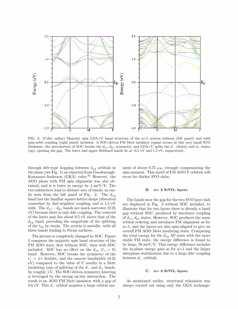
FIG. 2: (Color online) Majority spin LDA+U band structure of the n=1 system without (left panel) and withspin-orbit coupling (right panel) included. A SOC-driven FM Mott insulator regime occurs at this very small SVOthickness: the introduction of SOC breaks the dxz, dyz symmetry, and LDA+U splits the d− (down) and d+ states(up), opening the gap. The lower and upper Hubbard bands lie at -0.5 eV and 1.3 eV, respectively.
through ddπ-type hopping between dxy orbitals inthe plane (see Fig. 1) as expected from Goodenough-Kanamori-Anderson (GKA) rules.35 However, theAOO phase with FM spin alignment was also ob-tained, and it is lower in energy by 4 meV/V. Thetwo sublattices lead to distinct sets of bands, as eas-ily seen from the left panel of Fig. 2. The dxyband has the familiar square-lattice shape (distortedsomewhat by 2nd neighbor coupling, and is 1.5 eVwide. The dxz − dyz bands are much narrower (0.25eV) because there is only ddπ coupling. The centroidof the latter pair lies about 0.5 eV above that of thedxy band, providing the magnitude of the splittingof the t2g by strain. The system is metallic, with allthree bands leading to Fermi surfaces.
The picture is completely changed by SOC. Figure2 compares the majority spin band structure of theFM AOO state, first without SOC, then with SOCincluded. SOC has no effect on the dxy (ℓz = 0)band. However, SOC breaks the symmetry of theℓz = ±1 doublet, and the narrow bandwidth (0.25eV) compared to the value of U results in a Mottinsulating type of splitting of the d− and d+ bands,by roughly ±U. The SOC-driven symmetry loweringis leveraged by the strong on-site interaction. Theresult is an AOO FM Mott insulator with a gap of0.6 eV. This d− orbital acquires a large orbital mo-
ment of about 0.75 µB, strongly compensating thespin moment. This motif of FM AOO V orbitals willrecur for thicker SVO slabs.
B. n= 2 SrVO3 layers
The bands near the gap for the two SVO layer slabare displayed in Fig. 3 without SOC included, toillustrate that for two layers there is already a bandgap without SOC, produced by interlayer couplingof dxz, dyz states. However, SOC produces the sameorbital ordering and intralayer FM alignment as forn=1, and the layers are also spin-aligned to give anoverall FM AOO Mott insulating state. Comparingthe total energy for the dxy AF state with the morestable FM state, the energy difference is found tobe large, 76 meV/V. This energy difference includesthe in-plane energy gain as for n=1 and the largerinterplane stabilization due to a large ddσ couplingbetween d− orbitals.
C. n= 3 SrVO3 layers
As mentioned earlier, structural relaxation wasalways carried out using only the GGA exchange-
5
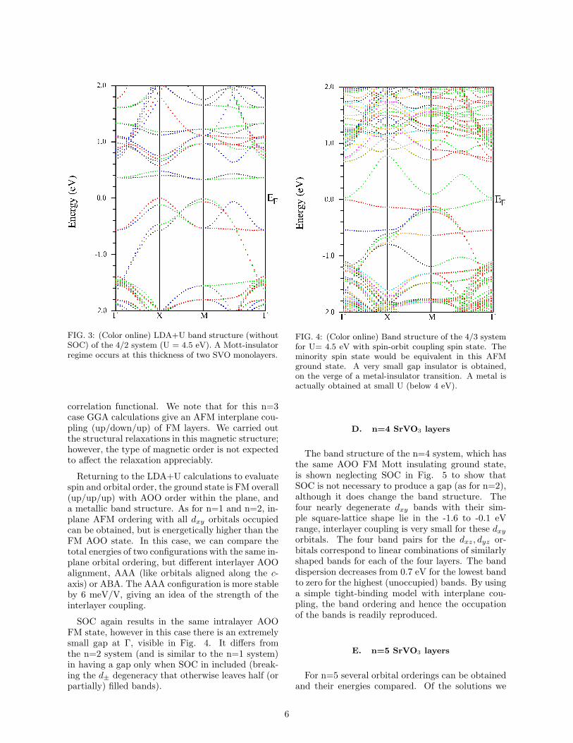
FIG. 3: (Color online) LDA+U band structure (withoutSOC) of the 4/2 system (U = 4.5 eV). A Mott-insulatorregime occurs at this thickness of two SVO monolayers.
correlation functional. We note that for this n=3case GGA calculations give an AFM interplane cou-pling (up/down/up) of FM layers. We carried outthe structural relaxations in this magnetic structure;however, the type of magnetic order is not expectedto affect the relaxation appreciably.
Returning to the LDA+U calculations to evaluatespin and orbital order, the ground state is FM overall(up/up/up) with AOO order within the plane, anda metallic band structure. As for n=1 and n=2, in-plane AFM ordering with all dxy orbitals occupiedcan be obtained, but is energetically higher than theFM AOO state. In this case, we can compare thetotal energies of two configurations with the same in-plane orbital ordering, but different interlayer AOOalignment, AAA (like orbitals aligned along the c-axis) or ABA. The AAA configuration is more stableby 6 meV/V, giving an idea of the strength of theinterlayer coupling.
SOC again results in the same intralayer AOOFM state, however in this case there is an extremelysmall gap at Γ, visible in Fig. 4. It differs fromthe n=2 system (and is similar to the n=1 system)in having a gap only when SOC in included (break-ing the d± degeneracy that otherwise leaves half (orpartially) filled bands).
FIG. 4: (Color online) Band structure of the 4/3 systemfor U= 4.5 eV with spin-orbit coupling spin state. Theminority spin state would be equivalent in this AFMground state. A very small gap insulator is obtained,on the verge of a metal-insulator transition. A metal isactually obtained at small U (below 4 eV).
D. n=4 SrVO3 layers
The band structure of the n=4 system, which hasthe same AOO FM Mott insulating ground state,is shown neglecting SOC in Fig. 5 to show thatSOC is not necessary to produce a gap (as for n=2),although it does change the band structure. Thefour nearly degenerate dxy bands with their sim-ple square-lattice shape lie in the -1.6 to -0.1 eVrange, interlayer coupling is very small for these dxyorbitals. The four band pairs for the dxz, dyz or-bitals correspond to linear combinations of similarlyshaped bands for each of the four layers. The banddispersion decreases from 0.7 eV for the lowest bandto zero for the highest (unoccupied) bands. By usinga simple tight-binding model with interplane cou-pling, the band ordering and hence the occupationof the bands is readily reproduced.
E. n=5 SrVO3 layers
For n=5 several orbital orderings can be obtainedand their energies compared. Of the solutions we
6
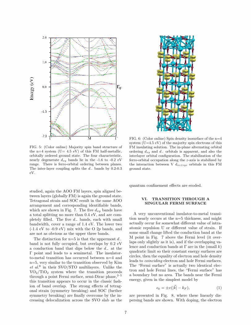
FIG. 5: (Color online) Majority spin band structure ofthe n=4 system (U= 4.5 eV) of this FM half-metallic,orbitally ordered ground state. The four characteristic,nearly degenerate dxy bands lie in the -1.6 to -0.2 eVrange. There is ferro-orbital ordering between planes.The inter-layer coupling splits the d− bands by 0.2-0.3eV.
studied, again the AOO FM layers, spin aligned be-tween layers (globally FM) is again the ground state.Tetragonal strain and SOC result in the same AOOarrangement and corresponding identifiable bands,which are shown in Fig. 7. The five dxy bands havea total splitting no more than 0.4 eV, and are com-pletely filled. The five d− bands, each with smallbandwidth, cover a range of 1.4 eV. The lower two(-1.4 eV to -0.9 eV) mix with the O 2p bands, andare not as obvious as the upper three bands.
The distinction for n=5 is that the uppermost d−band is not fully occupied, but overlaps by 0.2 eVa conduction band that dips below the d− at theΓ point and leads to a semimetal. The insulator-to-metal transition has occurred between n=4 andn=5, very similar to the transition observed by Kimet al.8 in their SVO/STO multilayers. Unlike theVO2/TiO2 system where the transition proceedsthrough a point Fermi surface, semi-Dirac phase,3–5
this transition appears to occur in the classic fash-ion of band overlap. The strong effects of tetrag-onal strain (symmetry breaking) and SOC (furthersymmetry breaking) are finally overcome by the in-creasing delocalization across the SVO slab as the
FIG. 6: (Color online) Spin density isosurface of the n=4system (U=4.5 eV) of the majority spin electrons of thisFM insulating solution. The in-plane alternating orbitalordering dxy and d− orbitals is apparent, and also theinterlayer orbital configuration. The stabilization of theferro-orbital occupation along the z-axis is stabilized bythe interaction between V dxz±iyz orbitals in this FMground state.
quantum confinement effects are eroded.
VI. TRANSITION THROUGH A
SINGULAR FERMI SURFACE
A very unconventional insulator-to-metal transi-tion nearly occurs at the n=5 thickness, and mightactually occur for somewhat different value of intra-atomic repulsion U or different value of strain. Ifsome small change lifted the conduction band at theM point in Fig. 7 above the Fermi level (it over-laps only slightly as it is), and if the overlapping va-lence and conduction bands at Γ are in the (small k)quadratic limit so their constant energy surfaces arecircles, then the equality of electron and hole densityleads to coinciding electron and hole Fermi surfaces.The “Fermi surface” is actually two identical elec-tron and hole Fermi lines, the “Fermi surface” hasa boundary but no area. The bands near the Fermienergy, given in the simplest model by
ǫk = ±v(|~k| − kF ), (1)
are presented in Fig. 8, where these linearly dis-persing bands are shown. With doping, the electron
7
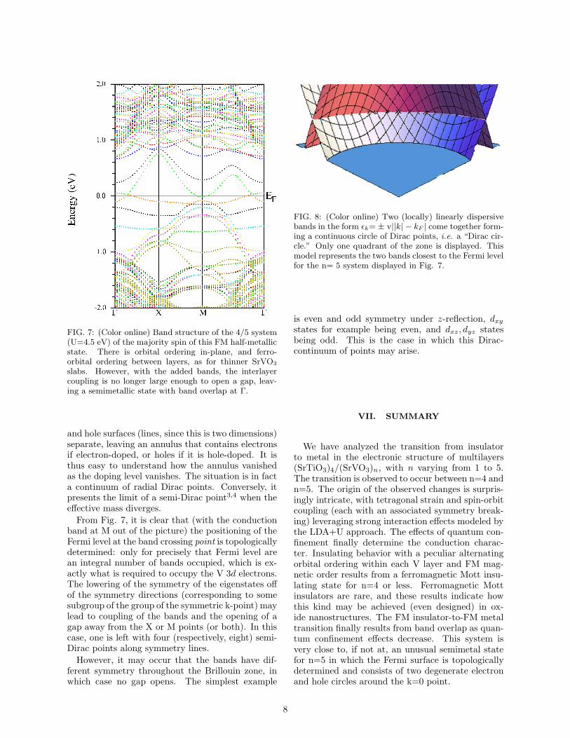
FIG. 7: (Color online) Band structure of the 4/5 system(U=4.5 eV) of the majority spin of this FM half-metallicstate. There is orbital ordering in-plane, and ferro-orbital ordering between layers, as for thinner SrVO3
slabs. However, with the added bands, the interlayercoupling is no longer large enough to open a gap, leav-ing a semimetallic state with band overlap at Γ.
and hole surfaces (lines, since this is two dimensions)separate, leaving an annulus that contains electronsif electron-doped, or holes if it is hole-doped. It isthus easy to understand how the annulus vanishedas the doping level vanishes. The situation is in facta continuum of radial Dirac points. Conversely, itpresents the limit of a semi-Dirac point3,4 when theeffective mass diverges.
From Fig. 7, it is clear that (with the conductionband at M out of the picture) the positioning of theFermi level at the band crossing point is topologicallydetermined: only for precisely that Fermi level arean integral number of bands occupied, which is ex-actly what is required to occupy the V 3d electrons.The lowering of the symmetry of the eigenstates offof the symmetry directions (corresponding to somesubgroup of the group of the symmetric k-point) maylead to coupling of the bands and the opening of agap away from the X or M points (or both). In thiscase, one is left with four (respectively, eight) semi-Dirac points along symmetry lines.
However, it may occur that the bands have dif-ferent symmetry throughout the Brillouin zone, inwhich case no gap opens. The simplest example
FIG. 8: (Color online) Two (locally) linearly dispersivebands in the form ǫk= ± v||k| − kF | come together form-ing a continuous circle of Dirac points, i.e. a “Dirac cir-cle.” Only one quadrant of the zone is displayed. Thismodel represents the two bands closest to the Fermi levelfor the n= 5 system displayed in Fig. 7.
is even and odd symmetry under z-reflection, dxystates for example being even, and dxz, dyz statesbeing odd. This is the case in which this Dirac-continuum of points may arise.
VII. SUMMARY
We have analyzed the transition from insulatorto metal in the electronic structure of multilayers(SrTiO3)4/(SrVO3)n, with n varying from 1 to 5.The transition is observed to occur between n=4 andn=5. The origin of the observed changes is surpris-ingly intricate, with tetragonal strain and spin-orbitcoupling (each with an associated symmetry break-ing) leveraging strong interaction effects modeled bythe LDA+U approach. The effects of quantum con-finement finally determine the conduction charac-ter. Insulating behavior with a peculiar alternatingorbital ordering within each V layer and FM mag-netic order results from a ferromagnetic Mott insu-lating state for n=4 or less. Ferromagnetic Mottinsulators are rare, and these results indicate howthis kind may be achieved (even designed) in ox-ide nanostructures. The FM insulator-to-FM metaltransition finally results from band overlap as quan-tum confinement effects decrease. This system isvery close to, if not at, an unusual semimetal statefor n=5 in which the Fermi surface is topologicallydetermined and consists of two degenerate electronand hole circles around the k=0 point.
8
VIII. ACKNOWLEDGMENTS
This project was supported by DOE grant DE-FG02-04ER46111 and through interactions with the
Predictive Capability for Strongly Correlated Sys-tems team of the Computational Materials ScienceNetwork.
∗ Electronic address: [email protected]† Electronic address: [email protected] N. Nakagawa, H. Y. Hwang, and D. A. Muller, Nat.Mater. 5, 204 (2006).
2 R. Pentcheva and W. E. Pickett, J. Phys.: Condens.Matter 22, 043001 (2010).
3 V. Pardo and W. E. Pickett, Phys. Rev. Lett. 102,166803 (2009).
4 S. Banerjee, R. R. P. Singh, V. Pardo, and W. E.Pickett, Phys. Rev. Lett. 103, 016402 (2009).
5 V. Pardo and W. E. Pickett, Phys. Rev. B 81, 035111(2010).
6 P. Dougier, J. C. C. Fan, and J. B. Goodenough, J.Solid State Chem. 14, 247 (1975).
7 E. Pavarini, S. Biermann, A. Poteryaev, A. I. Licht-enstein, A. Georges, and O. K. Andersen, Phys. Rev.Lett. 92, 176403 (2004).
8 D. H. Kim, D. W. Kim, B. S. Kang, T. W. Noh, D. R.Lee, K. B. Lee, and S. J. Lee, Solid State Commun.114, 473 (2000).
9 P. Hohenberg and W. Kohn, Phys. Rev. 136, B864(1964).
10 K. Schwarz and P. Blaha, Comp. Mat. Sci. 28, 259(2003).
11 E. Sjostedt, L. Nordstrom, and D. J. Singh, SolidState Commun. 114, 15 (2000).
12 J. P. Perdew, K. Burke, and M. Ernzerhof, Phys. Rev.Lett. 77, 3865 (1996).
13 V. I. Anisimov, J. Zaanen, and O. K. Andersen, Phys.Rev. B 44, 943 (1991).
14 E. R. Ylvisaker, W. E. Pickett, and K. Koepernik,Phys. Rev. B 79, 035103 (2009).
15 S. Biermann, A. Poteryaev, A. I. Lichtenstein, andA. Georges, Phys. Rev. Lett. 94, 026404 (2005).
16 J. M. Tomczak and S. Biermann, J. Phys.: Condens.Matter 19, 365206 (2007).
17 M. W. Haverkort, Z. Hu, A. Tanaka, W. Reichelt,S. V. Streltsov, M. A. Korotin, V. I. Anisimov, H. H.Hsieh, H. J. Lin, C. T. Chen, et al., Phys. Rev. Lett.95, 196404 (2005).
18 I. H. Inoue, O. Goto, H. Makino, N. E. Hussey, and
M. Ishikawa, Phys. Rev. B 58, 4372 (1998).19 Y. C. Lan, X. L. Chen, and M. He, J. Alloys Comp.
354, 95 (2003).20 M. Dawber, C. Lichtensteiger, M. Cantoni, M. Vei-
then, P. Ghosez, K. Johnston, K. M. Rabe, and J. M.Triscone, Phys. Rev. Lett. 95, 177601 (2005).
21 A. Ohtomo and H. Y. Hwang, Nature 427, 423 (2004).22 R. Pentcheva and W. E. Pickett, Phys. Rev. B 78,
205106 (2008).23 P. R. Willmott, S. A. Pauli, R. Herger, C. M.
Schleputz, D. Martoccia, B. D. Patterson, B. Delley,R. Clarke, D. Kumah, C. Cionca, et al., Phys. Rev.Lett. 99, 155502 (2007).
24 W. Siemons, G. Koster, H. Yamamoto, W. A. Harri-son, G. Lucovsky, T. H. Geballe, D. H. A. Blank, andM. R. Beasley, Phys. Rev. Lett. 98, 196802 (2007).
25 M. S. Park, S. H. Rhim, and A. J. Freeman, Phys.Rev. B 74, 205416 (2006).
26 R. Pentcheva and W. E. Pickett, Phys. Rev. B 74,035112 (2006).
27 S. S. A. Seo, M. J. Han, G. W. J. Hassink, W. S.Choi, S. J. Moon, J. S. Kim, T. Susaki, Y. S. Lee,J. Yu, C. Bernhard, H. Y. Hwang, G. Rijnders,D. H. A. Blank, B. Keimer,and T. W. Noh, Phys.Rev. Lett. 104, 036401 (2010).
28 A. Abragam and B. Bleaney, Electron paramagnetic
resonance of transition ions (Clarendon Press, Ox-ford, 1970).
29 W. H. Stevens, Proc. Royal Soc. London A 219, 542(1953).
30 J. B. Goodenough, Phys. Rev. 171, 466 (1968).31 C. Lacroix, J. Phys. C 13, 5125 (1980).32 W. E. Pickett and H. Eschrig, J. Phys.: Condens.
Matt. 19, 315203 (2007).33 G. Khaliullin and S. Maekawa, Phys. Rev. Lett. 85,
3950 (2000).34 K. W. Lee and W. E. Pickett, EPL 80, 37008 (2007).35 J. B. Goodenough, Magnetism and the chemical bond
(IEEE Press, New York, 2001).
9
Related Documents