University of Kentucky University of Kentucky UKnowledge UKnowledge Theses and Dissertations--Electrical and Computer Engineering Electrical and Computer Engineering 2015 ELECTRON-BEAM PATTERNING OF TEFLON AF FOR SURFACE ELECTRON-BEAM PATTERNING OF TEFLON AF FOR SURFACE PLASMON RESONANCE SENSING PLASMON RESONANCE SENSING Mansoor A. Sultan University of Kentucky, [email protected] Right click to open a feedback form in a new tab to let us know how this document benefits you. Right click to open a feedback form in a new tab to let us know how this document benefits you. Recommended Citation Recommended Citation Sultan, Mansoor A., "ELECTRON-BEAM PATTERNING OF TEFLON AF FOR SURFACE PLASMON RESONANCE SENSING" (2015). Theses and Dissertations--Electrical and Computer Engineering. 66. https://uknowledge.uky.edu/ece_etds/66 This Master's Thesis is brought to you for free and open access by the Electrical and Computer Engineering at UKnowledge. It has been accepted for inclusion in Theses and Dissertations--Electrical and Computer Engineering by an authorized administrator of UKnowledge. For more information, please contact [email protected].

Welcome message from author
This document is posted to help you gain knowledge. Please leave a comment to let me know what you think about it! Share it to your friends and learn new things together.
Transcript

University of Kentucky University of Kentucky
UKnowledge UKnowledge
Theses and Dissertations--Electrical and Computer Engineering Electrical and Computer Engineering
2015
ELECTRON-BEAM PATTERNING OF TEFLON AF FOR SURFACE ELECTRON-BEAM PATTERNING OF TEFLON AF FOR SURFACE
PLASMON RESONANCE SENSING PLASMON RESONANCE SENSING
Mansoor A. Sultan University of Kentucky, [email protected]
Right click to open a feedback form in a new tab to let us know how this document benefits you. Right click to open a feedback form in a new tab to let us know how this document benefits you.
Recommended Citation Recommended Citation Sultan, Mansoor A., "ELECTRON-BEAM PATTERNING OF TEFLON AF FOR SURFACE PLASMON RESONANCE SENSING" (2015). Theses and Dissertations--Electrical and Computer Engineering. 66. https://uknowledge.uky.edu/ece_etds/66
This Master's Thesis is brought to you for free and open access by the Electrical and Computer Engineering at UKnowledge. It has been accepted for inclusion in Theses and Dissertations--Electrical and Computer Engineering by an authorized administrator of UKnowledge. For more information, please contact [email protected].

STUDENT AGREEMENT: STUDENT AGREEMENT:
I represent that my thesis or dissertation and abstract are my original work. Proper attribution
has been given to all outside sources. I understand that I am solely responsible for obtaining
any needed copyright permissions. I have obtained needed written permission statement(s)
from the owner(s) of each third-party copyrighted matter to be included in my work, allowing
electronic distribution (if such use is not permitted by the fair use doctrine) which will be
submitted to UKnowledge as Additional File.
I hereby grant to The University of Kentucky and its agents the irrevocable, non-exclusive, and
royalty-free license to archive and make accessible my work in whole or in part in all forms of
media, now or hereafter known. I agree that the document mentioned above may be made
available immediately for worldwide access unless an embargo applies.
I retain all other ownership rights to the copyright of my work. I also retain the right to use in
future works (such as articles or books) all or part of my work. I understand that I am free to
register the copyright to my work.
REVIEW, APPROVAL AND ACCEPTANCE REVIEW, APPROVAL AND ACCEPTANCE
The document mentioned above has been reviewed and accepted by the student’s advisor, on
behalf of the advisory committee, and by the Director of Graduate Studies (DGS), on behalf of
the program; we verify that this is the final, approved version of the student’s thesis including all
changes required by the advisory committee. The undersigned agree to abide by the statements
above.
Mansoor A. Sultan, Student
Dr. J. Todd Hastings, Major Professor
Dr. Cai-Cheng Lu, Director of Graduate Studies

ELECTRON-BEAM PATTERNING OF TEFLON AF FOR SURFACE PLASMONRESONANCE SENSING
THESIS
A thesis submitted in partial fulfillmentof the requirements for the degree of
Master of Science in ElectricalEngineering in the College of
Engineering at the University ofKentucky
ByMansoor Sultan
Lexington, Kentucky
Director: Dr. J. Todd Hastings, Professor of Electrical EngineeringLexington, Kentucky 2015
Copyright c© Mansoor Sultan 2015

ABSTRACT OF THESIS
ELECTRON-BEAM PATTERNING OF TEFLON AF FOR SURFACE PLASMONRESONANCE SENSING
Variable pressure electron beam etching and lithography for Teflon AF has been demon-strated. The relation between dose and etching depth is tested under high vacuum andwater vapor. High resolution structures as small as 75 nm half-pitch have been resolved.Several simulation tools were tested for surface plasmon excitation. Grating based dualmode surface plasmon excitation has been shown numerically and experimentally.
KEYWORDS: Dual Mode Surface Plasmon, Grating Based SPR, VP-EBL, Teflon AFpatterning, Simulation.
Author’s signature: Mansoor Sultan
Date: April 30, 2015

ELECTRON-BEAM PATTERNING OF TEFLON AF FOR SURFACE PLASMONRESONANCE SENSING
ByMansoor Sultan
Director of Thesis: J. Todd Hastings
Director of Graduate Studies: Cai-Cheng Lu
Date: April 30, 2015

To my father and my family.

ACKNOWLEDGMENTS
I would never have been able to reach this stage without the guidance of my advisor, help
from friends, and support from my family and wife.
I would like to express my gratitude to my advisor, Dr. Hastings, for his guidance, patience,
and being available anytime I needed him.
I would like to thank Dr. Vijay Singh and Dr. Janet Lumpp for accepting to be on my thesis
defense committee.
I would also like to acknowledge National Science Foundation (NSF) and Jack and Linda
Gill Foundation for funding this work.
I would like to acknowledge The Higher Committee for Education Development in Iraq
(HCED) for supporting me to be here.
This work would be far more challenging without the help and guidance of my colleagues
in the Lab. Dr. Neha Nehru helped me to get started with surface plasmon theory and she
was my second resource after Dr. Hastings. Working with Dr. Lindsay Boehme was very
useful and her knowledge in chemistry and lithography was a great resource for me. Dr.
Carlos Jarro helped me to do my first surface plasmons excitation experiment. Samaneh
Esfandiarp and Adham Noubani, my classes and Lab colleagues, with them this journey
was more enjoyable, and they were always motivated to help and encourage me.
I would like to thank Mr. Brain Wajdyk, Jacob Hempel for training and guidance at Center
for Nanoscale Science and Engineering (CeNSE).
I would also like to thank my family and friend for their continuous support.
Finally, and most importantly, I would like to thank my wife Rasha, she was always there
with me in good and bad times.
iii

TABLE OF CONTENTS
Acknowledgments . . . . . . . . . . . . . . . . . . . . . . . . . . . . . . . . . . . . iii
Table of Contents . . . . . . . . . . . . . . . . . . . . . . . . . . . . . . . . . . . . iv
List of Tables . . . . . . . . . . . . . . . . . . . . . . . . . . . . . . . . . . . . . . vi
List of Figures . . . . . . . . . . . . . . . . . . . . . . . . . . . . . . . . . . . . . . vii
Chapter 1 : Surface Plasmon Resonance Principles . . . . . . . . . . . . . . . . . 11.1 Introduction . . . . . . . . . . . . . . . . . . . . . . . . . . . . . . . . . . 11.2 Fundamentals of Surface plasmon . . . . . . . . . . . . . . . . . . . . . . 31.3 Optical excitation of surface plasmon . . . . . . . . . . . . . . . . . . . . . 4
1.3.1 Prism configuration . . . . . . . . . . . . . . . . . . . . . . . . . . 41.3.2 Grating configuration . . . . . . . . . . . . . . . . . . . . . . . . . 11
1.4 Surface plasmon resonance sensors . . . . . . . . . . . . . . . . . . . . . . 14
Chapter 2 : Teflon AF Patterning for Surface Plasmon Sensing . . . . . . . . . . . 172.1 Introduction . . . . . . . . . . . . . . . . . . . . . . . . . . . . . . . . . . 172.2 Teflon AF patterning with variable pressure electron beam lithography (VP-
EBL) . . . . . . . . . . . . . . . . . . . . . . . . . . . . . . . . . . . . . . 182.2.1 Sample preparation and Teflon AF thin film coating . . . . . . . . . 192.2.2 Lithography process . . . . . . . . . . . . . . . . . . . . . . . . . 21
Chapter 3 : Sensor Design and Fabrication. . . . . . . . . . . . . . . . . . . . . . 293.1 Simulation tools . . . . . . . . . . . . . . . . . . . . . . . . . . . . . . . . 29
3.1.1 OptiScan . . . . . . . . . . . . . . . . . . . . . . . . . . . . . . . 303.1.2 S4: Stanford stratified structure solver . . . . . . . . . . . . . . . . 323.1.3 PhotonicsSHA 2D . . . . . . . . . . . . . . . . . . . . . . . . . . 34
3.2 Sensor chip design and fabrication . . . . . . . . . . . . . . . . . . . . . . 35
Chapter 4 : Results and Discussion . . . . . . . . . . . . . . . . . . . . . . . . . 384.1 Experimental setup . . . . . . . . . . . . . . . . . . . . . . . . . . . . . . 384.2 Experimental results . . . . . . . . . . . . . . . . . . . . . . . . . . . . . . 394.3 Simulation results . . . . . . . . . . . . . . . . . . . . . . . . . . . . . . . 424.4 Discussion . . . . . . . . . . . . . . . . . . . . . . . . . . . . . . . . . . . 46
Chapter 5 : Conclusion and Future Work . . . . . . . . . . . . . . . . . . . . . . 485.1 Conclusion . . . . . . . . . . . . . . . . . . . . . . . . . . . . . . . . . . 485.2 Future Work . . . . . . . . . . . . . . . . . . . . . . . . . . . . . . . . . . 49
Appendix A . . . . . . . . . . . . . . . . . . . . . . . . . . . . . . . . . . . . . . . 50
iv

References . . . . . . . . . . . . . . . . . . . . . . . . . . . . . . . . . . . . . . . . 51
Vita . . . . . . . . . . . . . . . . . . . . . . . . . . . . . . . . . . . . . . . . . . . 53
v

LIST OF TABLES
3.1 Exposure conditions for sensor fabrication. . . . . . . . . . . . . . . . . . . . . 37
vi

LIST OF FIGURES
1.1 The surface plasmon oscillations and electromagnetic fields . . . . . . . . . . . 21.2 Magnetic field exponential decay with the distance from interface in both medium 21.3 Kretschmann geometry of the attenuated total reflection (ATR) method for op-
tical surface plasmon excitation. . . . . . . . . . . . . . . . . . . . . . . . . . 51.4 The effective refractive index of a surface plasmon at a metal-dielectric inter-
face, with gold thickness of 50 nm and different angle of incidence. . . . . . . . 61.5 The reflectance of TM wave as a function of wavelength for a 500 nm Teflon
AF film coated with 55 nm gold film, with incident light through a BK7 prismat 65◦ incident angle inside the prism. . . . . . . . . . . . . . . . . . . . . . . 7
1.6 The reflectance as a function of angle of incidence for a 500 nm Teflon AFfilm coated with 55 nm gold film with incident light through a BK7 prism of awavelength 650 nm. . . . . . . . . . . . . . . . . . . . . . . . . . . . . . . . . 8
1.7 Otto geometry of the attenuated total reflection (ATR) method for optical sur-face plasmon excitation. . . . . . . . . . . . . . . . . . . . . . . . . . . . . . . 9
1.8 Field profile for symmetric and antisymmetric modes of surface plasmon wave. 101.9 The dispersion relation for the surface plasmon modes of a thin metal film be-
tween two dielectrics. The metal thickness of 50 nm and the angle of incidenceis 66.5◦ and the light incident through a BK7 prism. . . . . . . . . . . . . . . . 10
1.10 Reflectance as function of wavelength for a 500 nm Teflon AF film coated witha 55 nm gold film with incident light through a BK7 prism at a 65◦ incidentangle for dual mode excitation. . . . . . . . . . . . . . . . . . . . . . . . . . . 11
1.11 Grating based surface plasmon excitation configuration. . . . . . . . . . . . . . 121.12 Normalized wave vectors for surface plasmon wave and first positive (m =+1)
diffracted wave as a function of wavelength and angle of incidence. . . . . . . . 131.13 Dual surface plasmon excitation with grating configuration . . . . . . . . . . . 141.14 Block diagram of optical SPR sensor. . . . . . . . . . . . . . . . . . . . . . . 15
2.1 Chemical structure of Teflon AF [1]. . . . . . . . . . . . . . . . . . . . . . . . 172.2 Teflon AF patterning process, . . . . . . . . . . . . . . . . . . . . . . . . . . . 182.3 Teflon AF film thickness as function of spinning speed and dilution ratio. . . . 202.4 Teflon AF refractive index as function of wavelength measured by ellipsometry. 202.5 Dose vs. Depth for e-beam exposure of Teflon AF using [a] 10 keV, [b] 20
keV, and [c] 30 keV beam energies under high-vacuum and 1 Torr water vaporconditions before and after development. . . . . . . . . . . . . . . . . . . . . . 22
2.6 Threshold and contrast estimation plot for 1 Torr water vapor condition afterdevelopment [a] 10 keV, [b] 20 keV, and [c] 30 keV. . . . . . . . . . . . . . . 24
2.7 Nested lines with 750 nm half-pitch, exposed with a beam energy of 10 keVand a dose of 1,300 pC/cm with 1 Torr H2O pressure. . . . . . . . . . . . . . 25
2.8 Nested lines with 150 nm half-pitch, exposed with beam energy of 10 keV anda dose of 5,200 pC/cm with 1 Torr H2O pressure. . . . . . . . . . . . . . . . 26
vii

2.9 Nested lines with 75 nm half-pitch, exposed with beam energy 10 keV and adose of 5,200 pC/cm with 1 Torr H2O pressure. . . . . . . . . . . . . . . . . 27
2.10 Nested lines with 38 nm half-pitch, exposed with beam energy 10 keV and adose of 1,300 pC/cm with 1 Torr H2O pressure. . . . . . . . . . . . . . . . . . 28
3.1 Design tested with OptiScan. . . . . . . . . . . . . . . . . . . . . . . . . . . . 313.2 Diffraction efficiency as a function of wavelength and number or orders for the
grating structure in Figure (3.1). . . . . . . . . . . . . . . . . . . . . . . . . . 323.3 Reflectance as a function of wavelength and number of orders for the grating
structure in Figure (3.1) tested with the S4 tool from the nanohub website. . . . 333.4 Diffraction efficiency as a function of wavelength and number of orders for the
grating structure in Figure (3.1) tested with PhotonicsSHA 2D. . . . . . . . . . 353.5 Grating period test for dual mode excitation with grating structure. . . . . . . . 36
4.1 Experimental setup for sensor chip testing. . . . . . . . . . . . . . . . . . . . . 394.2 SEM image for a grating structure that supports dual surface plasmons exci-
tation. The grating period is 430 nm. The image was taken after the opticalmeasurements due to carbon deposition and etching of the Teflon with highbeam energies. . . . . . . . . . . . . . . . . . . . . . . . . . . . . . . . . . . 40
4.3 Experimental results for reflectance as a function of wavelength for TE andTM modes for the grating shown in Figure(4.2). The TM mode shows singlemode excitation for SPR around 630 nm. . . . . . . . . . . . . . . . . . . . . . 41
4.4 Experimental results for reflectance as a function of wavelength for TE andTM modes for the grating shown in Figure(4.2). The TM mode shows SRSPand LRSP excitation at 590 nm and 645 nm, respectively. . . . . . . . . . . . . 42
4.5 Dispersion relation for surface plasmon excitation [a] Single mode, [b] Dualmode. . . . . . . . . . . . . . . . . . . . . . . . . . . . . . . . . . . . . . . . 43
4.6 Approximate design for the grating structure in Figure (4.2) was used for sim-ulation with PhotonicsSHA 2D. . . . . . . . . . . . . . . . . . . . . . . . . . . 44
4.7 TM to TE ratio as function of wavelength for experimental and simulationresults [a] Single mode, [b] Dual mode. . . . . . . . . . . . . . . . . . . . . . 45
4.8 Refractive index for water and Teflon as function of wavelength. . . . . . . . . 464.9 TM to TE ratio as a function of wavelength and grating depth simulated by
PhotonicsSHA 2D for a 430 nm grating period with different depths. . . . . . . 47
viii

Chapter 1 : Surface Plasmon Resonance Principles
1.1 Introduction
In 1902, Wood observed sharp dark bands in the diffracted light from a metallic diffraction
grating, and he called them as anomalies [2]. Fifty-six years later, Thurbadar identified a
complete adsorption in the reflectivity of a thin metal film [3]. However, both of them did
not identify these observation as surface plasmon resonance (SPR). In 1968, Otto explained
similar results; the drop in reflectivity of the thin metal film was due to SPR [4]. The deriva-
tion of surface plasmon is based on the plasma configuration of Maxwell’s equations, where
the free electrons of the metal are considered as the plasma. Plasma oscillation in metals is
aggregative longitudinal excitations of the conductive electron gas (see Figure (1.1)), and
plasmon are the quanta that represent these charge-density oscillations. The charge-density
fluctuations can be exist in the bulk media or bound at metal-dielectric interface, where they
spread as waves along the interface forming what called surface plasmon. The propagating
electron density oscillations create surface-localized electromagnetic waves. The electro-
magnetic fields of these waves is perpendicular to the boundary, and they exponentially
decay as they propagate in the medium as shown in Figure (1.2). These electromagnetic
fields are produced optically under the conditions of total internal reflection at the boundary
between the metal and dielectric media. However, the electric and magnetic fields do not
stop at the boundary. Rather they propagate into the medium as a surface wave. Despite the
fact that Maxwell’s equations explained the presence of surface waves and demonstrated
them in the first decade of the twentieth century, the surface plasmon field had not been
studied until 1960, and the term ’surface plasmon’ was coined later in the 1960s. It was
proven that Maxwell’s equations can solve the surface plasmon field under two conditions.
First, one of the media has to have a negative real part of its complex dielectric constant
ε. Second, the component of the wave vector ( which will be refereed to later as kx) along
1

the interface between these two media, must fulfill an equation that includes the dielectric
constants of both media [5].
- - - + + + - - - + + + - - -
z
x
Hy
(ε )Dielectric d
(ε )Metal m
Figure 1.1: The surface plasmon oscillations and electromagnetic fields
−3 −2 −1 0 1 2 3 4 5 6
0.0
0.1
0.2
0.3
0.4
0.5
0.6
0.7
0.8
0.9
1.0
z−position (µm)
Hy
(arb
. u
nit
s)
Metal Dielectric
Figure 1.2: Magnetic field exponential decay with the distance from interface in both
medium
2

1.2 Fundamentals of Surface plasmon
If we assume the two media have semi-infinite length (x),oscillations on the boundary
between the two media have electromagnetic fields that can be described by the following
equations, and depicted in Figure (1.2):
Hyd = H0 e(−γd z) e(− jkx x) f or z > 0
Exd = E0 e(−γd z) e(− jkx x) f or z > 0
Hym = H0 e(+γm z) e(− jkx x) f or z < 0
Exm = E0 e(+γm z) e(− jkx x) f or z < 0 (1.1)
With
γd =√
kx−εdk20
γm =√
kx−εmk20
where k0 =2π
λ= ω
c ( free space wave vector) and kx = k0 ne f f
By introducing the dielectric constants for the active surface plasmon medium (metal) as
εm (εm = ε′m + jε′′m) and εd for the adjacent medium (dielectric), and solving Maxwell’s
equations and boundary conditions we get:
k2x + γ
2d = εm(
ω
c)
2
k2x + γ
2m = εd(
ω
c)
2
and by solving for wave vector kx we get:
kx =ω
c
√εmεd
εm +εd(1.2)
where c is the speed of light in vacuum and ω is the angular frequency of surface plasmon
wave. from the equation above we can conclude
ne f f =
√εmεd
εm +εd(1.3)
3

1.3 Optical excitation of surface plasmon
Surface plasmons can be excited with different methods, such as prism coupling [4, 6],
grating coupling [7] and waveguide coupling [8]. The most common ways for surface
plasmon resonance sensing are the prism and grating configuration; therefore, we will
discuss these methods only.
1.3.1 Prism configuration
In the last section, we mentioned that Maxwell’s equations have a solution for surface plas-
mon only when one of the media has a negative real part of its dielectric constant. For this
reason, this condition is valid in gold and silver over specific wavelength range. Further-
more, in order to excite surface plasmon by light, the electric field has to have a continuous
tangential component along the interface and wave vector match the surface plasmon wave
vector (kx). The later (kx) is given by equation (1.3) [5]. In the prism coupling, there are
two geometries: Kretschmann geometry [6] and Otto geometry [4]. Both configurations
depend on a prism coupler and the attenuated total reflection method (ATR). Kretschmann
geometry consists of a metal-dielectric interface coupled with a prism, which is shown in
Figure (1.3) below. The material propertes in this thesis for the gold and glass are taken
from references [9, 10]. Teflon AF optical properties were determined using the Cauchy
formula for dispersion fit to the measurements of Lowry et al. [11].
4

SP
θ
Prism (n )p
Metal
Dielectric
Incident light Reflected light
Figure 1.3: Kretschmann geometry of the attenuated total reflection (ATR) method for
optical surface plasmon excitation.
When the light penetrates through the prism and reflects from the surface of the metal film,
part of this light propagates in the metal film as an evanescent electromagnetic field. The
evanescent field couples with surface plasmon at the boundary with the dielectric layer.
This coupling only happens when the metal film is adequately thin.The wave vector of the
surface plasmon penetrating the metal layer, KSP, is affected by the dielectric layer and has
the following formula:
kSP = kSP0 +∆k =ω
c
√εmεd
εm +εd+∆k (1.4)
Where ∆k is the effect of prism and metal thickness.
As we mentioned before, surface plasmon can only be excited when the evanescent wave
vector (kEW ) matches the surface plasmon vector (kSP):
kEW = kSP
5
kEW =2π
λnp sinθ
KSP = Re
{2π
λ
√εmεd
εm +εd
}where np is the refractive index of the prism and θ is the angle of incident inside the prism.
2π
λnp sinθ = Re
{2π
λ
√εmεd
εm +εd
}+∆k (1.5)
Solving for the effective refractive index:
np sinθ = ne f f +∆n = Re
{√εmεd
εm +εd
}+∆n (1.6)
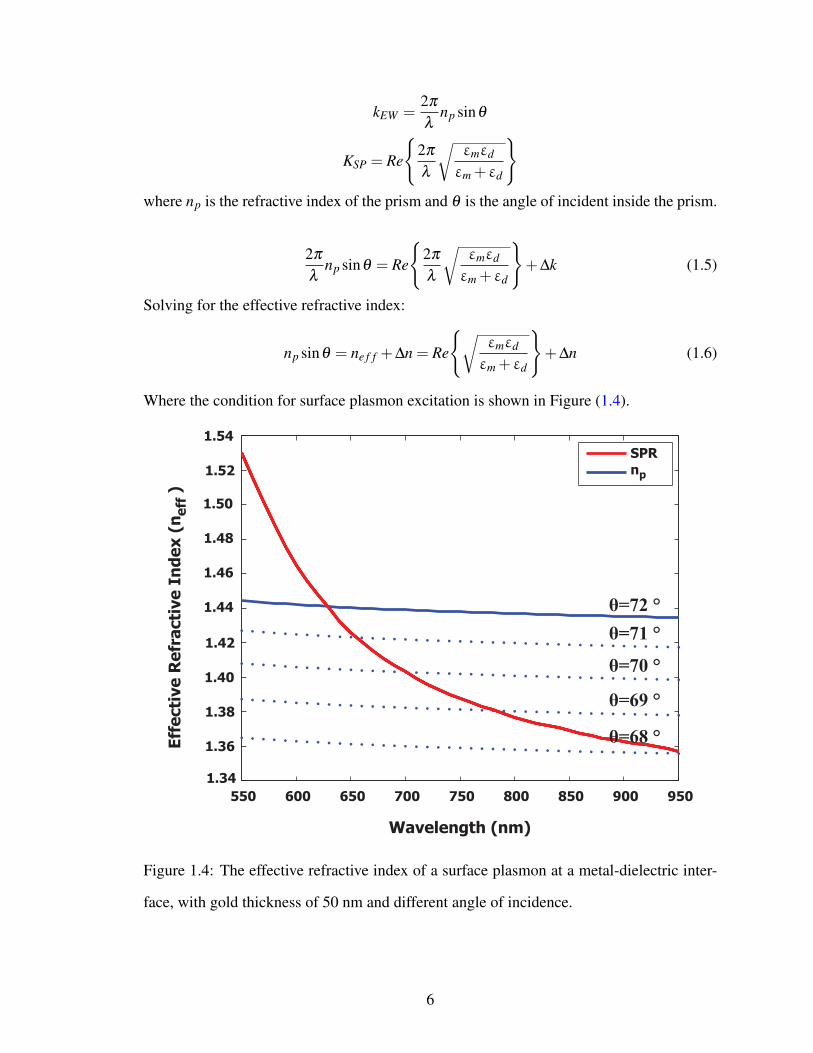
Where the condition for surface plasmon excitation is shown in Figure (1.4).
550 600 650 700 750 800 850 900 950
1.34
1.36
1.38
1.40
1.42
1.44
1.46
1.48
1.50
1.52
1.54
Wavelength (nm)
Eff
ecti
ve
Re
fra
cti
ve
In
de
x (
ne
ff)
SPR
np
θ=72 °
θ=71 °
θ=70 °
θ=69 °
θ=68 °
Figure 1.4: The effective refractive index of a surface plasmon at a metal-dielectric inter-
face, with gold thickness of 50 nm and different angle of incidence.
6

We can see the effect on light reflectance by Kretschmann geometry as shown in Figure
(1.5).
400 500 600 700 800 900 1000 11000
0.1
0.2
0.3
0.4
0.5
0.6
0.7
0.8
0.9
1.0
Wavelength (nm)
Re
fle
cta
nce
Figure 1.5: The reflectance of TM wave as a function of wavelength for a 500 nm Teflon AF
film coated with 55 nm gold film, with incident light through a BK7 prism at 65◦ incident
angle inside the prism.
If we choose a wavelength where the real part of the dielectric of metal is negative, and
sweep the angle of incidence the surface plasmon excitation will occurs at specific angle
that satisfy equation(1.6) as shown in the Figure (1.6) below.
7

50 55 60 65 70 75 80
0
0.1
0.2
0.3
0.4
0.5
0.6
0.7
0.8
0.9
1
Angle (degree)
Re
fle
cta
nce
Figure 1.6: The reflectance as a function of angle of incidence for a 500 nm Teflon AF film
coated with 55 nm gold film with incident light through a BK7 prism of a wavelength 650
nm.
In Otto geometry, the layers have a different arrangement which is shown in Figure (1.7).
There is a few microns gap between the prism and metal. In order to satisfy the coupling
condition, the evanescent wave and plasmon wave have to have equal wave vectors. The
derivation of surface plasmon wave vector follows the Kretschmann geometry.
8

SP
θ
Prism (n )p
Metal
Air
Incident light Reflected light
Figure 1.7: Otto geometry of the attenuated total reflection (ATR) method for optical sur-
face plasmon excitation.
Radan et al. and Hastings et al. have reported more advanced sensor design by excit-
ing symmetric and antisymmetric surface plasmons, or what are called short range surface
plasmon (SRSP) and long range surface plasmon (LRSP) [12, 13]. This excitation was
achieved by upgrading Kretschmann geometry by introducing a dielectric layer between
the prism and metal layer with optical properties that match the dielectric layer on top. The
field profile of symmetric and antisymmetric modes is shown in Figure (1.8). The excita-
tion for dual modes occurs when the metal thickness is less than 100 nm. The matching
condition for the effective refractive index and the two modes is shown in Figure (1.9), and
the reflectance curve as function of wavelength is shown in Figure (1.10)
9

Metal
Dielectric 1
Dielectric 1
h < 100nm
Sym
Figure 1.8: Field profile for symmetric and antisymmetric modes of surface plasmon wave.
550 600 650 700 750 800 850 900 950
1.30
1.35
1.40
1.45
1.50
1.55
1.60
1.65
1.70
Wavelength (nm)
ne
ff
SRSP
LRSP
np
Figure 1.9: The dispersion relation for the surface plasmon modes of a thin metal film
between two dielectrics. The metal thickness of 50 nm and the angle of incidence is 66.5◦
and the light incident through a BK7 prism.
10

400 500 600 700 800 900 1000 1100
0
0.1
0.2
0.3
0.4
0.5
0.6
0.7
0.8
0.9
1.0
Wavelength (nm)
Re
fle
cta
nce
Figure 1.10: Reflectance as function of wavelength for a 500 nm Teflon AF film coated
with a 55 nm gold film with incident light through a BK7 prism at a 65◦ incident angle for
dual mode excitation.
1.3.2 Grating configuration
The other common method for surface plasmon excitation is a metal grating. In this con-
figuration, the incident light from dielectric medium on a metal grating with period Λ is
shown in Figure (1.11). The wave vector of the diffracted wave must match the wave vector
of the surface plasmon wave:
kdi f f =2π
λnd sinθ +m
2π
Λ(1.7)
ksp =±2π
λRe
{√εmεd
εm +εd
}+∆k (1.8)
2π
λnd sinθ +m
2π
Λ=±2π
λRe
{√εmεd
εm +εd
}+∆k (1.9)
11

Where nd is the refractive index of dielectric, θ is angle of incident wave, λ is incident
wavelength, ∆k is the effect of presence of grating, and m is the diffraction order. Re-
arranging the equation above, we get:
nd sinθ +mλ
Λ=±Re
{√εmεd
εm +εd
}+∆ ne f f (1.10)
where
∆ ne f f = Re
{∆kλ
2π
}
ne f f =±Re
{√εmεd
εm +εd
}+∆ ne f f (1.11)
m=1
m=2
m=3
m=-1
m=-2
m=-3
θ
Figure 1.11: Grating based surface plasmon excitation configuration.
Referring to the previous equations (1.9,1.10), it can be seen that the coupling condition
can be achieved with different design. For example, if we consider grating made of gold
with a period (Λ = 680 nm) and incident light from water with a variable angle, we get
coupling at different wavelengths as shown in Figure (1.12).
12

550 600 650 700 750 800 850 900 950
1
1.1
1.2
1.3
1.4
1.5
1.6
Wavelength (nm)
SP
KDiff
K
No
rma
lize
d w
ave
ve
cto
rs
θ = 7
˚θ=18 ˚
θ = 2
8 ˚
Figure 1.12: Normalized wave vectors for surface plasmon wave and first positive (m=+1)
diffracted wave as a function of wavelength and angle of incidence.
Vala et al. have reported dual mode excitation for SRSP and LRSP with a grating config-
uration and employed them for SPR sensing [14]. The excitation theory of the symmetric
and antisymmetric is identical to the prism configuration, a dielectric grating is coated with
a thin metal film. Hence, the matching condition similar to grating configuration and de-
pends on the grating period and modulation of the grating. Dual mode excitation with a
diffraction grating is shown in Figure (1.13).
13

Λ
h
Dielectric 2
Dielectric 1
Metal
incident light
m=1m=-1
m=-2 m=2
Figure 1.13: Dual surface plasmon excitation with grating configuration .
1.4 Surface plasmon resonance sensors
The use of surface plasmon for optical sensing dates back to the early of 1980s, when
surface plasmon sensors were used for studying electrochemical reactions [15]. Many
surface plasmon resonance (SPR) sensors have been developed since then. The optical
SPR sensor is an instrument composed of light source, a detector, a sensor-chip, an analyte
injection unit, and a data processing unit (see Figure (1.14)). As mentioned previously, the
excitation of surface plasmon causes changes in the output light properties. SPR sensors
can be utilized to sense changes in light properties, and depending on the affected property,
the SPR can be interrogated by detecting changes in wavelength, angle, intensity, phase, or
polarization. The first three types of interrogation are the most common [16].
14
Light source Sensor & sample injection unit Light detector
Data processing unitOutput
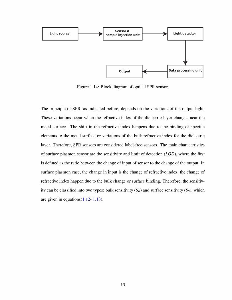
Figure 1.14: Block diagram of optical SPR sensor.
The principle of SPR, as indicated before, depends on the variations of the output light.
These variations occur when the refractive index of the dielectric layer changes near the
metal surface. The shift in the refractive index happens due to the binding of specific
elements to the metal surface or variations of the bulk refractive index for the dielectric
layer. Therefore, SPR sensors are considered label-free sensors. The main characteristics
of surface plasmon sensor are the sensitivity and limit of detection (LOD), where the first
is defined as the ratio between the change of input of sensor to the change of the output. In
surface plasmon case, the change in input is the change of refractive index, the change of
refractive index happen due to the bulk change or surface binding. Therefore, the sensitiv-
ity can be classified into two types: bulk sensitivity (SB) and surface sensitivity (SS), which
are given in equations(1.12- 1.13).
15

SB =δλSP
δn
(nm−wavelength
RIU
)
SB =δθSP
δn
(degreeRIU
)(1.12)
SS =δλSP
t
(nm−wavelength
nm−binding thickness
)
SS =δθSP
t
(degree
nm−binding thickness
)(1.13)
where (RIU) means refractive index unit.
The (LOD) is the minimum change that the sensor can detect in the bulk refractive index,
a layer thickness or concentration. LOD is divided into bulk (LODB) and surface (LODS):
LODB =3σSP
SB(1.14)
LODS =3σSP
SS(1.15)
where σSP : is the standard deviation of measured λSP, θSP, or ISP with respect to the sensor
type.
Copyright c© Mansoor Sultan, 2015.
16

Chapter 2 : Teflon AF Patterning for Surface Plasmon Sensing
2.1 Introduction
Teflon AF is a class of amorphous fluoropolymers that has unique properties such as a low
dielectric constant, high optical clarity, and low refractive index. In addition, the chemical
structure of Teflon AF, shown in Figure (2.1), provides it with high chemical and thermal
resistance [1]. On account of these properties, Teflon AF has gained significant interest
in the following applications: semiconductors, biomedical, fiber-optics, optical materials,
photonics and plasmonic sensing techniques. The diversity of these applications has led to
the development of several methods for Teflon AF patterning. These include reactive ion
beam milling, direct electron beam lithography and UV lithography based process [17–19].
Recently, a new patent demonstrated the ability of using Teflon AF as a negative electron
beam resist [20].
Figure 2.1: Chemical structure of Teflon AF [1].
17

2.2 Teflon AF patterning with variable pressure electron beam lithography (VP-EBL)
The high demand for Teflon AF patterning, the difficulty of writing a grating on gold for
grating-based surface plasmon excitation, and our intention to excite the short and long
range of surface plasmon resonance by grating-based configuration, all motivated us to
study new ways for Teflon AF patterning. The proposed method is depicted in (Figure 2.2)
below and discussed in subsequent sections.
Silicon
Silicon
Adhesion promoter
Silicon
Silicon
Adhesion promoter
Te!on AF
Silicon
E-beam
Silicon
Development with Ethanol
Silicon
Spin coating adhesion
spin coating Te!on AF
Pro"lometer measurements
Pro"lometer measurements
Figure 2.2: Teflon AF patterning process,
18

2.2.1 Sample preparation and Teflon AF thin film coating
Depending on the application, the substrate was either a microscope slide with properties
similar to BK7 or silicon wafer. The BK7 substrate was used for sensor fabrication, and the
silicon wafer was used for lithography study. The BK7-slide were cleaved into 1x1 square
inches, and cleaned by ultrasonication in acetone, ethanol and water for 5 minutes for each
solvent to remove impurities and glass particles due to the cleaving process. The Teflon AF
solution has a high viscosity as purchased; therefore, it was diluted with FC-40 (3 M Inc.)
to different weight ratios from 1 : 2.5 to 1 : 6 determined by the required thickness of the
film. Since Teflon AF is non-adherent to the glass and silicon surfaces, it was necessary to
coat the sample with an adhesion promoter layer. The adhesion promoter was prepared by
mixing a fluorosilane, 1H,1H, 2H, 2H perfluorodecyltriethoxy silane (Lancaster Synthesis,
Inc.), ethanol, and DI-water with weight ratio (1 : 95 : 5). The adhesion layer was spun at
2000 RPM for 10 seconds, and baked at 110 ◦Cfor 10 minutes. The diluted Teflon AF resist
were spun at 500 RPM for 10 seconds to form a uniform layer; then spun at different speeds
from 1000 RPM to 6000 RPM to determine the appropriate speed for the proper thickness,
and baked at 165 ◦C. Finally, ellipsometry was used (Ellipsometer M-200, J.A. Woollam
Co. Inc.) to measure the film thickness, where the Teflon AF layer fit as a Cauchy material
model. Figure (2.3) shows the speed versus thickness for each ratio of dilution (Teflon
AF to FC-40), and Figure (2.4) shows the optical properties of Teflon AF film on a silicon
wafer.
19

3000 3500 4000 4500 5000 5500 600050
100
150
200
250
300
350
400
450
500
Spinning Speed (RPM)
Fil
m T
hic
kn
ess (
nm
)
1:2.5
1:3.5
1:4.5
1:6
Figure 2.3: Teflon AF film thickness as function of spinning speed and dilution ratio.
400 500 600 700 800 900 1000
1.304
1.306
1.308
1.310
1.312
1.314
1.316
1.318
Wavelength(nm)
Re
fra
cti
ve
in
de
x (
n)
Figure 2.4: Teflon AF refractive index as function of wavelength measured by ellipsometry.
20

2.2.2 Lithography process
Low resolution features
In this step, we employed variable-pressure electron-beam lithography (VP-EBL), typi-
cally used to mitigate charging, for positive tone patterning of Teflon AF. This process
eliminates problems associated with lifting off spin coated films, provides complete mate-
rial removal (unlike direct patterning), and minimally affects the properties of the undevel-
oped Teflon (unlike negative tone processes). Rectangles (25µm×100µm) were exposed
in spin-coated Teflon AF films (480-nm thick) using beam energies of 10, 20, and 30 keV.
Exposures were conducted under either high vacuum (∼ 5×10⁻⁵ Torr) or 1 Torr of water
vapor in a FEI environmental scanning electron microscope (ESEM) with a Raith ELPHY
Plus pattern generator. Samples were developed for 120 seconds in ethanol, and a pro-
filometer was used to measure the pattern depth before and after development.
Plots of pattern depth vs. dose in Figure (2.5) confirm that a significant relief pattern is
present before development for both high-vacuum and 1 Torr H2O exposures. However,
water vapor does not appear to accelerate pattern formation through e-beam induced etch-
ing. For high-vacuum exposures, development revealed both positive and negative tone
behavior at lower and higher doses respectively; however, the pattern failed to clear under
all conditions. For exposure in water vapor, positive tone behavior was observed with full
clearance. This dramatic difference may be associated with radiation induced reactions
involving water, as the radiation degradation of Teflon depends strongly on the ambient
environment [21].
21

[a]10
010
110
210
310
4
−500
−450
−400
−350
−300
−250
−200
−150
−100
−50
0
Dose (μC/cm )
De
pth
(n
m)
1 torr (H O) Before
High Vacuum Before
1 torr (H O) After
High Vacuum After
2
2
2
[b]10
0
101
102
103
104
−500
−450
−400
−350
−300
−250
−200
−150
−100
−50
0
Dose (µC/cm )
Depth (nm)
1 torr (H O) Before
High Vacuum Before
High Vacuum After
2
1 torr (H O) After
2
2
[c]10
0
101
102
103
104
−500
−450
−400
−350
−300
−250
−200
−150
−100
−50
0
De
pth
(n
m)
Dose (μC/cm )
1 torr (H O) Before
High Vacuum Before
1 torr (H O) After
High Vacuum After
2
2
2
Figure 2.5: Dose vs. Depth for e-beam exposure of Teflon AF using [a] 10 keV, [b] 20
keV, and [c] 30 keV beam energies under high-vacuum and 1 Torr water vapor conditions
before and after development.
22

Depths were measured both before and after development in ethanol as noted in the legends.
High vacuum exposures exhibited both positive and negative tone behavior but failed to
clear (note minima near 900 and 2000 µC/cm2 at 10 and 20 keV respectively). However,
exposure under water vapor yielded positive tone behavior and clearing doses from 500 to
1000 µC/cm2. The threshold dose and contrast was estimated by using Figure (2.6) and
equation (2.1).
γ =[log(D100
D0
)]−1(2.1)
Where D0 is the the threshold dose for resist removal, D100 is the dose for complete resist
removal, and Figure (2.6) shows how they were calculated. Estimated contrasts were 1.5,
2.9, and 2.0 for 10, 20, and 30 keV respectively.
23

[a]10
110
210
30
50
100
150
200
250
300
350
400
450
Dose(μC/cm )2
Re
ma
inin
g R
esis
t T
hic
kn
ess (
nm
)
Real Data
Line Fit
Resist Thickness
D100
D0
[b]10
1
102
103
0
50
100
150
200
250
300
350
400
450
Re
ma
inin
g R
esis
t T
hic
kn
ess (
nm
)
Real Data
Line Fit
Resist Thickness
Dose(μC/cm )2
D0
D100
[c]10
110
210
30
50
100
150
200
250
300
350
400
450
2
Re
ma
inin
g R
esis
t T
hic
kn
ess (
nm
)
Real Data
Line Fit
Resist Thickness
Dose(μC/cm )
D0
D100
Figure 2.6: Threshold and contrast estimation plot for 1 Torr water vapor condition after
development [a] 10 keV, [b] 20 keV, and [c] 30 keV.
24

High resolution features
For using Teflon AF as a resist, we explored the highest resolution that can be achieved
with thinner films. Different sets of nested lines were exposed into an 80 nm film under
1 Torr pressure and beam energies of 10 keV, 20 keV, and 30 keV. The exposed nested
lines were: 15 nm to 500 nm half-pitch with doses ranging from 2,000 to 14,600 pC/cm
and step size of 24 nm. After exposure and development for 120 second with ethanol, the
sample was coated with a thin gold layer (around 8 nm) to mitigate charging and protect the
sample from etching during the imaging. SEM imaging of the structures revealed pithes
approximately 1.5 times larger than the desired size. This implies that the writing field is
larger by the same ratio and the dose is lower by the same factor. The smallest half-pitch
observed on the sample was 75 nm. Figures (2.7 - 2.10 ) show the high resolution structures
with the exact dimensions and doses.
5 µm
Figure 2.7: Nested lines with 750 nm half-pitch, exposed with a beam energy of 10 keV
and a dose of 1,300 pC/cm with 1 Torr H2O pressure.
25

3 µm
Figure 2.8: Nested lines with 150 nm half-pitch, exposed with beam energy of 10 keV and
a dose of 5,200 pC/cm with 1 Torr H2O pressure.
26

2 µm
Figure 2.9: Nested lines with 75 nm half-pitch, exposed with beam energy 10 keV and a
dose of 5,200 pC/cm with 1 Torr H2O pressure.
27

1 µm
Figure 2.10: Nested lines with 38 nm half-pitch, exposed with beam energy 10 keV and a
dose of 1,300 pC/cm with 1 Torr H2O pressure.
Copyright c© Mansoor Sultan, 2015.
28

Chapter 3 : Sensor Design and Fabrication.
3.1 Simulation tools
Chapter 1 provided a brief overview of dual mode SPR excitation using a dielectric grating
coated with a metal layer. Chapter 2 discussed the protocol developed in our lab for fabri-
cating gratings for SPR sensing applications. This chapter examines the various simulation
tools used to study the response of grating based SPR sensors. Three simulation tools
were tested [22–24]. These tools all depend on rigorous coupled wave theory (RCWT) to
solve multilayered structures, but each one has a different algorithm. RCWT is a precise
solution for Maxwell’s equations for an incident wave on multilayered structures, where
the electromagnetic fields are expressed by Fourier series [25]. The accuracy of RCWT is
determined by the number of orders that were used for field and material properties. Dual
mode grating based SPR sensor simulations with these tools was challenging due to differ-
ent reasons for each tool. The next sections discuss each tool and its respective advantages
and disadvantages.
29

3.1.1 OptiScan
OptiScan is a matlab based graphical user interface (GUI) simulation tool, developed by
the Milster group at Arizona University [22]. This tool is used for 2D optical system
simulations and it has a wide range of applications. One of its accessories is the RCWT
calculator, which we used for a sensor design test. Keathley and Hastings utilized this
code for nano-gap enhanced SPR sensors, and it revealed reliable matching between the
simulation and test results [26]. OptiScan is characterized by a user friendly interface and
user prescribed material properties, where the user can use the required material properties
as tabulated data for wavelength (in µm), real part of refractive index and imaginary part
of refractive index. However, this code was not efficient with longer period and multilayer
structures, and the calculation time increased as the grating period increased. In addition,
if the structure contains metals, it requires twice the minimum number of order (N). The
minimum number of order is define as:
N = 2Λ/λ
Where Λ is the grating period and λ is the incident wavelength. Further simulations have
been carried out with the RCWT calculator; code did not converge quickly and there was
a deviation between the order number and code convergence. The design in Figure (3.1)
was tested with the RCWT calcualtor in OptiScan, and it was discovered that increasing
the order number did not improve the accuracy of the calculation. Results of the diffraction
efficiency for the the design are shown in Figure (3.2).
30

350 nm
50 nm
Water
500 nm Teflon
BK7
Gold
Incident Light
Figure 3.1: Design tested with OptiScan.
31

4 5 6 7 8 9 10
x 10−7
0.0
0.1
0.2
0.3
0.4
0.5
0.6
0.7
Wavelength(meters)
Dif
fra
cti
on
Eff
icie
ncy
10 order
20 order
25 order
35 order
40 order
80 order
140 order
Figure 3.2: Diffraction efficiency as a function of wavelength and number or orders for the
grating structure in Figure (3.1).
3.1.2 S4: Stanford stratified structure solver
S4 is another simulation tool used to implement RCWT calculations for 2D and 3D struc-
tures based on C/C++ language [23]. The code was published in 2012 and first released
on the nanohub website for Purdue University in April 2013. The online version has two
programing methods: a graphical user interface or script writing. The GUI is limited to
certain materials, therefore, we used the script writing method, where we can specify the
desired material properties. The paper disclosed that S4 is not efficient with metal gratings,
we used the code anticipating that this limitation had been addressed in newer versions,
the latest version have been published in August 2014. Unfortunately, the code did not
work well with metal-dielectric gratings, and the solution did not converge as we increased
the number of orders. The design used for testing this code is illustrated in Figure (3.1).
32

A different number of orders were tested for the same design, and the resulting curve for
reflectance is shown in Figure (3.3). The code written for this design is given in detail in
Appendix A.
400 500 600 700 800 900 1000
0.0
0.1
0.2
0.3
0.4
0.5
0.6
0.7
Wavelength(nm)
Re
fle
cta
nce
5 orders
10 orders
20 orders
30 orders
45 orders
60 orders
85 orders
Figure 3.3: Reflectance as a function of wavelength and number of orders for the grating
structure in Figure (3.1) tested with the S4 tool from the nanohub website.
,
33

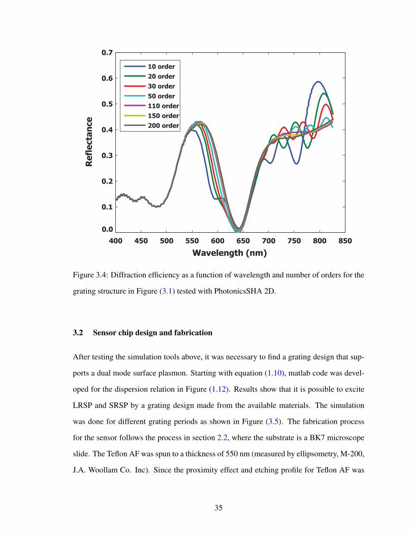
3.1.3 PhotonicsSHA 2D
PhotnonicsSHA 2D is a spatial harmonic analysis code developed by Xingjie Ni et al.,
and released online on the nanohub website [24]. The code solver was written in C with a
linear algebraic package (LAPACK). The GUI was written with Qt and Qwt libraries. This
tool has a user friendly GUI, and it is very useful for 2D multilayer grating simulation.
The design in Figure (3.1) was tested with photonicsSHA 2D and the results obtained
showed better convergence than the previous two tools. However, this tool does not allow
for the addition and use of materials outside of its limited database, which proved to be
major disadvantage for our sensor design. Therefore, for the design shown in Figure 3.1,
water was used instead of Teflon AF and the simulation wavelength range was limited to
826 nm because the database does not include water dielectric constant values above that
wavelength. The results of the tested design are depicted in Figure (3.4), which shows
a consistent profile of the reflectance and better convergence with higher order numbers.
This tool was selected for our design simulation and testing.
34
400 450 500 550 600 650 700 750 800 850
0.0
0.1
0.2
0.3
0.4
0.5
0.6
0.7
Wavelength (nm)
Re
fle
cta
nce
10 order
20 order
30 order
50 order
110 order
150 order
200 order
Figure 3.4: Diffraction efficiency as a function of wavelength and number of orders for the
grating structure in Figure (3.1) tested with PhotonicsSHA 2D.
3.2 Sensor chip design and fabrication
After testing the simulation tools above, it was necessary to find a grating design that sup-
ports a dual mode surface plasmon. Starting with equation (1.10), matlab code was devel-
oped for the dispersion relation in Figure (1.12). Results show that it is possible to excite
LRSP and SRSP by a grating design made from the available materials. The simulation
was done for different grating periods as shown in Figure (3.5). The fabrication process
for the sensor follows the process in section 2.2, where the substrate is a BK7 microscope
slide. The Teflon AF was spun to a thickness of 550 nm (measured by ellipsometry, M-200,
J.A. Woollam Co. Inc). Since the proximity effect and etching profile for Teflon AF was
35

unknown, sets of single pixel lines and rectangles with different geometry were exposed on
the sample to identify which geometry will be useful for surface plasmon excitation. The
rectangles and line length is 200 µm. The exposure conditions are tabulated in table (3.1).
After etching, the sample was developed with ethanol for 120 seconds and coated with a
thin gold film by RF deposition. The gold thickness was 46 nm.
550 600 650 700 750 800
1.0
1.5
2.0
2.5
Wavelength (nm)
ne
ff
SRSP
LRSP
KDiff
Λ = 350 nm
Λ = 430 nm
Λ = 550 nm
Figure 3.5: Grating period test for dual mode excitation with grating structure.
36

Table 3.1: Exposure conditions for sensor fabrication.
PPPPPPPPPPPPPPPParameter
Width305 nm 365 nm Single pixel Single pixel
Pitch (nm) 730 855 305 430
Beam energy (keV) 30
Beam current (nA) 172
Area dose (µC/cm2)135 135 - -
335 335 - -
Line dose (pC/cm)
- - 8200 8200
- - 6560 6560
- - 9835 9835
H2O pressure (Torr) 1
Step size (nm) 20
Copyright c© Mansoor Sultan, 2015.
37
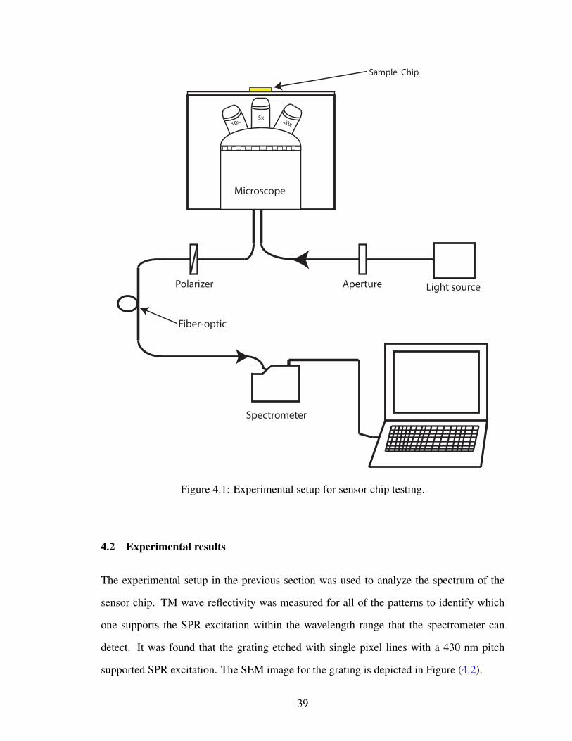
Chapter 4 : Results and Discussion
4.1 Experimental setup
Chapter three provided a detailed description for the sensor chip fabrication and simulation
tools. In order to test the chip, The experimental setup consisted of a microscope (Carl
Zeiss:Axiovert 405 M) and a spectrometer (Ocean optics HR4000CG-UV-NIR) with Spec-
trasuite software package, was used to analyze the sample spectrum as shown in Figure
(4.1). The etched patterns were on a 200 square micrometers area; therefore, it was nec-
essary to use a microscope to adjust the incident light on the patterned area. The sample
was mounted to the microscope stage and the light was normally incident on the sample.
The aperture was used to control the illumination field to obtain reflected light from only
the zero order of the patterned area. As mentioned previously in chapter one, the excita-
tion of surface plasmons occurs with transverse magnetic waves. Thus, a polarizer was
used to filter the reflected light from the sample either as transverse electric (TE) or trans-
verse magnetic (TM) polarized waves. In addition, a silver coated mirror was used as for
reference spectrum.
38
5x
10x 20x
Sample Chip
Fiber-optic
Spectrometer
Polarizer Light source
Microscope
Aperture
Figure 4.1: Experimental setup for sensor chip testing.
4.2 Experimental results
The experimental setup in the previous section was used to analyze the spectrum of the
sensor chip. TM wave reflectivity was measured for all of the patterns to identify which
one supports the SPR excitation within the wavelength range that the spectrometer can
detect. It was found that the grating etched with single pixel lines with a 430 nm pitch
supported SPR excitation. The SEM image for the grating is depicted in Figure (4.2).
39
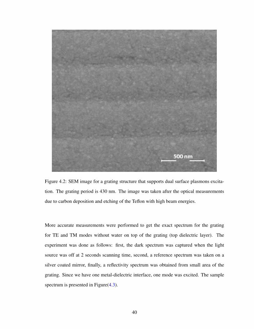
Figure 4.2: SEM image for a grating structure that supports dual surface plasmons excita-
tion. The grating period is 430 nm. The image was taken after the optical measurements
due to carbon deposition and etching of the Teflon with high beam energies.
More accurate measurements were performed to get the exact spectrum for the grating
for TE and TM modes without water on top of the grating (top dielectric layer). The
experiment was done as follows: first, the dark spectrum was captured when the light
source was off at 2 seconds scanning time, second, a reference spectrum was taken on a
silver coated mirror, finally, a reflectivity spectrum was obtained from small area of the
grating. Since we have one metal-dielectric interface, one mode was excited. The sample
spectrum is presented in Figure(4.3).
40

450 500 550 600 650 700 750 800
0
20
40
60
80
100
120
Wavelength (nm)
Re
fle
cta
nce
TE
TM
Figure 4.3: Experimental results for reflectance as a function of wavelength for TE and TM
modes for the grating shown in Figure(4.2). The TM mode shows single mode excitation
for SPR around 630 nm.
The experiment was repeated with water on top of the grating and SRSP and LRSP were
excited as shown in Figure(4.4).
41

450 500 550 600 650 700 750 800
0
20
40
60
80
100
120
Wavelength (nm)
Re
fle
cta
nce
TE
TM
Figure 4.4: Experimental results for reflectance as a function of wavelength for TE and
TM modes for the grating shown in Figure(4.2). The TM mode shows SRSP and LRSP
excitation at 590 nm and 645 nm, respectively.
4.3 Simulation results
Since the etching profile and proximity effects were unknown, several simulations were
carried out to understand and analyze the resulting spectra. First, we used the matlab
code to calculate the dispersion relation (effective index vs. wavelength) for the surface
plasmon modes and it shows a perfect match between the experimental (Figures( 4.3 ,4.4))
and simulated results as shown in Figure (4.5). where the resonance wavelength can be
found from the intersection of Kdi f f with SRSP and LRSP indexes. It can be seen that
resonance wavelengths are 625 nm, 594 nm, and 653 nm for single mode, SRSP, and
LRSP, respectively.
42
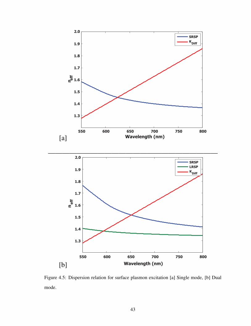
[a]550 600 650 700 750 800
1.3
1.4
1.5
1.6
1.7
1.8
1.9
2.0
Wavelength (nm)
n eff
SRSP
KDiff
————————————————————————
[b]550 600 650 700 750 800
1.3
1.4
1.5
1.6
1.7
1.8
1.9
2.0
Wavelength (nm)
ne
ff
SRSP
LRSP
KDiff
Figure 4.5: Dispersion relation for surface plasmon excitation [a] Single mode, [b] Dual
mode.
43

Second, PhotonicsSHA 2D was used to simulate the grating structure mentioned pre-
viously. The simulated design is shown in Figure(4.6) where the depth of the etched area
set to be 51 nm and the top layer set to be either air or water. The reflectance spectrum was
simulated for TE and TM modes.
BK7 Substrate
Teflon AF
Au
Air / Water
570 nm
46 nm77 nm
Incident light
430 nm
120 nm
Figure 4.6: Approximate design for the grating structure in Figure (4.2) was used for sim-
ulation with PhotonicsSHA 2D.
44

The resulting reflectance spectrum had a shift with the resonance wavelength for both
single and dual mode excitation. For comparison between experimental and simulated
results, the ratio of TM to TE mode was taken, as shown in Figure (4.7).
[a]400 450 500 550 600 650 700 750 800
0.0
0.2
0.4
0.6
0.8
1.0
1.2
1.4
Wavelength (nm)
TM
/T
E
Experimental
Simulation
——————————————————————-
[b]400 450 500 550 600 650 700 750 800
0.0
0.2
0.4
0.6
0.8
1.0
1.2
1.4
Wavelength (nm)
TM
/T
E
Experimental
Simulation
Figure 4.7: TM to TE ratio as function of wavelength for experimental and simulation
results [a] Single mode, [b] Dual mode.
45

4.4 Discussion
The results clearly show that there is a shift in the resonance wavelength between the ex-
perimental and simulated spectra. Several reasons could account for this discrepancy. First,
in the simulation with PhotonicsSHA 2D water was used instead of Telfon AF because the
database does not contain optical properties for Teflon AF. Although the optical properties
are similar, they are not equal. Figure (4.8) shows the refractive index for water and Teflon
AF as function of wavelength.
400 450 500 550 600 650 700 750 800 850
1.20
1.22
1.24
1.26
1.28
1.30
1.32
1.34
1.36
1.38
1.40
Wavelength (nm)
Re
fra
cti
ve
in
de
x
water
Teflon
Figure 4.8: Refractive index for water and Teflon as function of wavelength.
Second, the depth and shape of the grating are unknown; we know the period of the grating
only. Right edges were used to represent the trench of the grating (Figure (4.6)) while it
looks like rounded edges in the real image for the grating (Figure (4.2)). Further simula-
tions were done with different grating trench depth, and it was discovered that the depth
of grating shifts the resonance wavelength and change the reflectance profile as shown in
Figure (4.9).
46

400 450 500 550 600 650 700 750 8000
0.1
0.2
0.3
0.4
0.5
0.6
0.7
0.8
0.9
1
Wavelength (nm)
TM
/T
E
31 nm
36 nm
41 nm
Figure 4.9: TM to TE ratio as a function of wavelength and grating depth simulated by
PhotonicsSHA 2D for a 430 nm grating period with different depths.
Copyright c© Mansoor Sultan, 2015.
47

Chapter 5 : Conclusion and Future Work
5.1 Conclusion
Over the last five decades, SPR sensors have gained great interest, as they introduce label
free sensors with real time sensing. Various approaches have been reported for SPR excita-
tion and sensing: single or multi-mode. This document provides basic level understanding
of SPR theory and sensors, as well as an easy method for dual mode SPR excitation using
grating structures, where a VP-EBL method was employed for Teflon patterning. Teflon
patterning with VP-EBL with chemical development revealed a remarkable improvement
for Teflon AF patterning in comparison with direct EBL. A lower clearing dose and full
clearance for exposed Teflon AF was observed with this technique. The positive tone be-
havior with complete Teflon removal can be linked to an induced radiation reaction in the
presence of water vapor, or the radiation degradation of Teflon, which is highly dependent
on the chamber environment.This method not only provides a very useful mechanism for
SPR sensors fabrication, but also for 3D lithography and nano-imprinting. High resolution
structures with up to 75 nm half-pitch were patterned on 80 nm thickness samples.
For sensor design, several simulation tools were explored. The advantages and disadvan-
tages of each were addressed and only one packaged converged for the structures con-
sidered in this work. A series of experiments were designed to test the SPR supporting
structures, and single and dual mode excitation for SPR were observed with this method.
The results from these experiments and simulations proved that dual SPR excitation oc-
cours, which can be used for self-referencing SPR sensors. In this method, the light is
incident from the back of the sensor chip, unlike the grating based SPR, where the light is
incident from the top through the analyte, making fluid cell fabrication much easier.
48

5.2 Future Work
The experimental and simulation results in this work show interesting outcomes, namely
Teflon patterning to obtain dual mode SPR excitation. Results can be improved by several
approaches. Teflon AF patterning can be improved by studying interaction of Teflon with
the electron beam in the presence of water vapor, since little is known in this area. In this
work, only one value for the of water vapor pressure was tested (1 Torr). To obtain the pro-
cess limitations, a range of water vapor pressure could be scanned. The effect of chemical
developer (ethanol was used in the present study) is another factor. The reaction of the ex-
posed area with ethanol is unclear, and stronger solvents, such as N-Methyl-2-pyrrolidone
(NMP), to examine their effect on the patterns etched into Teflon.
One of the challenges of this work is the simulation. It was difficult to simulate the design
with the tools explored:OptiScan, S4 and PhotonicsSHA 2D. PhotonicsSHA 2D was useful
for simulations with limited material properties and wavelength range. Testing other simu-
lation tools could improve and make simulations more practical, especially if the material
properties can be prescribed by the user. Milling a designated area of the pattern with a
focused ion beam (FIB) and imaging the cross section of the grating would give a precise
view of the grating shape, making the simulations more accurate. Finally, increasing the
Teflon AF thickness and making the light incident with different angles could lead to better
results, such as the SPR reflectivity dip width which will improve the sensitivity and LOD.
Copyright c© Mansoor Sultan, 2015.
49

Appendix A
S4 code for the design in Figure (3.1).S = S4 . NewSimula t ion ( )S : S e t L a t t i c e ({3 5 0 . 0 0 0 0 0 0 , 0 . 0 0 0 0 0 0} ,{0 . 0 0 0 0 0 0 , 0 . 0 0 0 0 0 0} )S : SetNumG ( 1 0 0 )S : AddMate r i a l ( ”BK7” , {2 . 3 4 3 4 9 5 , 0 . 0 0 0 0 0 0} )S : AddMate r i a l ( ” T e f l o n ” , {1 . 7 3 5 7 0 6 2 6 3 , 0 . 0 0 0 0 0 0} )S : AddMate r i a l ( ” AU JC ” , {−1.658092 ,5 .735356} )S : AddMate r i a l ( ”HO2” , {1 . 7 9 2 9 2 1 , 0 . 0 0 0 0 0 0} )S : AddLayer ( ’ Layer Above ’ , 0 . 0 0 0 0 0 0 , ’BK7 ’ )S : AddLayer ( ’ l a y e r 1 ’ , 500 .000000 , ’ Tef lon ’ )S : AddLayer ( ’ l a y e r 2 ’ , 50 .000000 , ’ Tef lon ’ )S : S e t L a y e r P a t t e r n R e c t a n g l e ( ’ l a y e r 2 ’ , ’ AU JC ’ , {8 7 . 5 0 , 0 . 0 0 0} , 0 . 0 0 , {8 7 . 5 0 , 0 . 0 0} )S : AddLayer ( ’ l a y e r 3 ’ , 50 .000000 , ’AU JC ’ )S : S e t L a y e r P a t t e r n R e c t a n g l e ( ’ l a y e r 3 ’ , ’HO2’ , {8 7 . 5 0 , 0 . 0 0} , 0 . 0 0 , {8 7 . 5 0 , 0 . 0 0} )S : AddLayer ( ’ Layer Below ’ , 0 . 0 0 0 0 0 0 , ’HO2’ )S : S e t E x c i t a t i o n P l a n e w a v e ({ 0 . 0 0 , 0 . 0 0} ,{ 0 . 0 0 , 0 . 0 0} ,{ 1 . 0 0 , 0 . 0 0} )f r e q u e n c y = { Frequency v e c t o r = 1 / w a v e l e n g t h } ;r e a l e p s 1 = {BK7 r e a l p a r t o f t h e d i e l e c t r i c c o n s t a n t f o r t h e f r e q u e n c y v e c t o r } ;i m a g e p s 1 = { BK7 i m a g i n a r y p a r t o f t h e d i e l e c t r i c c o n s t a n t f o r t h e f r e q u e n c y v e c t o r } ;r e a l e p s 2 = {T e f l o n AF r e a l p a r t o f t h e d i e l e c t r i c c o n s t a n t f o r t h e f r e q u e n c y v e c t o r } ;i m a g e p s 2 = {T e f l o n i m a g i n a r y p a r t o f t h e d i e l e c t r i c c o n s t a n t f o r t h e f r e q u e n c y v e c t o r } ;r e a l e p s 3 = { go ld r e a l p a r t o f t h e d i e l e c t r i c c o n s t a n t f o r t h e f r e q u e n c y v e c t o r } ;i m a g e p s 3 = { go ld i m a g i n a r y p a r t o f t h e d i e l e c t r i c c o n s t a n t f o r t h e f r e q u e n c y v e c t o r } ;r e a l e p s 4 = {w a t e r r e a l p a r t o f t h e d i e l e c t r i c c o n s t a n t f o r t h e f r e q u e n c y v e c t o r } ;i m a g e p s 4 = {w a t e r i m a g i n a r y p a r t o f t h e d i e l e c t r i c c o n s t a n t f o r t h e f r e q u e n c y v e c t o r } ;f o r i = 1 , 601 do
f r e q = f r e q u e n c y [ i ] ;S : S e t F r e q u e n c y ( f r e q )S : S e t M a t e r i a l ( ’BK7’ , { r e a l e p s 1 [ i ] , i m a g e p s 1 [ i ] } ) ;S : S e t M a t e r i a l ( ’ Tef lon ’ , { r e a l e p s 2 [ i ] , i m a g e p s 2 [ i ] } ) ;S : S e t M a t e r i a l ( ’ AU JC ’ , { r e a l e p s 3 [ i ] , i m a g e p s 3 [ i ] } ) ;S : S e t M a t e r i a l ( ’HO2’ , { r e a l e p s 4 [ i ] , i m a g e p s 4 [ i ] } ) ;i n c i d e n c e f l u x , r e f l e c t i o n f l u x B K 7 = S : G e t P o y n t i n g F l u x ( ’ Layer Above ’ , 0 . 0 0 0 0 0 0 )r e f l e c t i o n f l u x B K 7 = (−1) ∗ r e f l e c t i o n f l u x B K 7 / i n c i d e n c e f l u x ;t r a n s m i s s i o n f l u x = S : G e t P o y n t i n g F l u x ( ’ Layer Below ’ , 0 . 0 0 0 0 0 0 )t r a n s m i s s i o n f l u x H O 2 = t r a n s m i s s i o n f l u x / i n c i d e n c e f l u x ;i n c i d e n c e f l u x B K 7 = i n c i d e n c e f l u x / i n c i d e n c e f l u x ;p r i n t ( 1 / f r e q . . ’\ t ’ . . r e f l e c t i o n f l u x B K 7 ) ;
end
50

References
[1] H. Zhang and S. G. Weber, Fluorous Chemistry. Springer Berlin Heidelberg, 2012,vol. 308, ch. Teflon AF material, pp. pp 307–337.
[2] R. W. Wood, “Xlii. on a remarkable case of uneven distribution of light in a diffractiongrating spectrum,” The London, Edinburgh, and Dublin Philosophical Magazine andJournal of Science., vol. 4, no. 21, pp. 396–402., 1902.
[3] T. Turbadar, “Complete absorption of light by thin metal films.” Proceedings of thePhysical Society, vol. 73, no. 1, pp. 40–44, 1959.
[4] A. Otto, “Excitation of nonradiative surface plasma waves in silver by the method offrustrated total reflection.” Zeitschrift fur Physik, vol. 216, no. 4, pp. 398–410, 1968.[Online]. Available: http://dx.doi.org/10.1007/BF01391532
[5] Z. Salamon and G. Tollin, “Surface plasmon resonance, theory,” vol. 3, pp. 2804–2812, 1999.
[6] K. Erwin and H. Raether, “Radiative decay of non-radiative surface plasmons excitedby light,” Z. Naturforsch. a, vol. 23, no. 12, pp. 2135–2136, 1968.
[7] R. H. Ritchie et al., “Surface-plasmon resonance effect in grating diffraction,”Physical Review Letters, vol. 21, no. 22, pp. 1530–1533, November 1968. [Online].Available: http://link.aps.org/doi/10.1103/PhysRevLett.21.1530
[8] J. DostA¡lek et al., “Surface plasmon resonance biosensor based on integratedoptical waveguide,” Sensors and Actuators B: Chemical, vol. 76, no. 1-3, pp. 8– 12, 2001, proceeding of the Eighth International Meeting on Chemical SensorsIMCS-8 - Part 1. [Online]. Available: http://www.sciencedirect.com/science/article/pii/S0925400501005597
[9] P. B. Johnson and R. W. Christy, “Optical constants of the noble metals,”Phys. Rev. B, vol. 6, pp. 4370–4379, Dec 1972. [Online]. Available: http://link.aps.org/doi/10.1103/PhysRevB.6.4370
[10] Data sheet for N-BK7, SCHOTT north America Inc., 2007.
[11] J. H. Lowry et al., “Optical characteristics of the teflon af fluoro-plastic materials,”pp. 142–151, 1991. [Online]. Available: http://dx.doi.org/10.1117/12.47534
[12] R. Slavık et al., “Advanced biosensing using simultaneous excitation of short andlong range surface plasmons,” Measurement Science and Technology, vol. 17, no. 4,pp. 932–938, 2006.
[13] J. T. Hastings et al., “Optimal self-referenced sensing using long- and short- rangesurface plasmons,” Optical Society of America, 2007.
51

[14] M. Vala et al., “Diffraction grating-coupled surface plasmon resonance sensor basedon spectroscopy of long-range and short-range surface plasmons,” 2007. [Online].Available: http://dx.doi.org/10.1117/12.723131
[15] J. G. II and S. Ernst, “Surface plasmons as a probe of the electrochemical interface,”Surface Science, vol. 101, no. 1-3, pp. 499 – 506, 1980. [Online]. Available:http://www.sciencedirect.com/science/article/pii/0039602880906445
[16] O. S.Wolfbeis, Surface Plasmon Resonance Based Sensors, ser. Springer Series OnChemical Sensor And Biosensor, H. J., Ed. Springer, 2006, vol. 4.
[17] M. W. Denhoff and M. Gao, “Patterning amorphous fluoropolymer films by reactiveion milling,” M. W. Denhoff, vol. 26, no. 8, pp. 941–943, 1997. [Online]. Available:http://dx.doi.org/10.1007/s11664-997-0278-2
[18] V. Karre et al., “Direct electron-beam patterning of teflon af,” IEEE TRANSACTIONSON NANOTECHNOLOGY, vol. 8, no. 2, pp. 139–141, 2009.
[19] I. Czolkos et al., “High-resolution micropatterned teflon af substrates forbiocompatible nanofluidic devices,” Langmuir, vol. 28, no. 6, pp. 3200–3205, 2012.[Online]. Available: http://pubs.acs.org/doi/abs/10.1021/la2044784
[20] A. Jesorka and M. Shaali, “Lithographic pattern development process for amorphousfluoropolymer,” U.S. Patent US20 140 065 551 A1, 2014. [Online]. Available:http://www.google.com/patents/US20140065551
[21] W. Burger et al., “Radiation degradation of fluoropolymers: Carboxylated fluoropoly-mers from radiation degradation in presence of air,” Journal of Applied Polymer Sci-ence, vol. 48, no. 11, pp. 1973–1985, June 1993.
[22] T. Milster, “Optiscan,” 2012. [Online]. Available: http://www.optics.arizona.edu/Milster/optiscan/OptiScan MENU PAGE.htm
[23] J. Kang et al., “S4: Stanford stratified structure solver,” Apr 2013. [Online].Available: https://nanohub.org/resources/15167
[24] X. Ni et al., “Photonicssha-2d: Modeling of single-period multilayer optical gratingsand metamaterials,” Aug 2009. [Online]. Available: https://nanohub.org/resources/6977
[25] M. G. Moharam and T. K. Gaylord, “Rigorous coupled-wave analysis of planar-grating diffraction,” J. Opt. Soc. Am., vol. 71, no. 7, pp. 811–818, Jul 1981. [Online].Available: http://www.opticsinfobase.org/abstract.cfm?URI=josa-71-7-811
[26] P. D. Keathley and J. T. Hastings, “Nano-gap-enhanced surface plasmon resonancesensors,” Plasmonics, vol. 7, pp. 59–69, 2012.
52
Vita
Mansoor Sultan was born in Bayji, Iraq. He received his B.Eng from the department of
medical instrumentations engineering at the Technical college of Mosul in Nenevah, Iraq.
He worked for 7 years at Bayji Gas power plant in Bayji, Iraq, as an operation engineer.
In 2010, he got a sponsorship from Higher Committee for Education in Iraq (HCED) to
pursue a Master of Science (M.Sc) degree in Electrical Engineering. He started his M.Sc
in Electrical Engineering at the University of Kentucky, in Lexington, in August 2013.
53
Related Documents