Electron backscatter diffraction analysis of electrodeposited nano-scale copper wires Y. Ke a , T. Konkova b, ⁎, S. Mironov c , K. Tamahashi b , J. Onuki b a Graduate School of Science and Engineering, Ibaraki University, Hitachi, Ibaraki 316-8511, Japan b Department of Materials Science and Engineering, Ibaraki University, Hitachi, Ibaraki 316-8511, Japan c Department of Materials Processing, Graduate School of Engineering, Tohoku University, 6-6-02 Aramaki-aza-Aoba, Sendai 980-8579, Japan abstract article info Article history: Received 30 May 2012 Received in revised form 15 April 2013 Accepted 8 May 2013 Available online 23 May 2013 Keywords: Electrodeposition Copper Nano-crystalline Electron backscatter diffraction The high-resolution electron backscatter diffraction technique was applied to study grain-size, misorientation distribution and texture, which affect resistivity substantially, in electrodeposited and subsequently annealed nano-scale (80 nm width) copper wires. Particular emphasis was given to the examination of the variation of the microstructural parameters and texture in the trench thickness direction. The bottom part of the wires was shown to be characterized by the largest proportion of low-angle boundaries and the lowest fraction of annealing twins. The crystallographic texture of the wires was also demonstrated to significantly change in thick- ness direction. Depending on the trench height, the close packed {111} plane was shown to align either with the side walls or the bottom surface. © 2013 Elsevier B.V. All rights reserved. 1. Introduction The ongoing miniaturization of electronic devices has prompted the reduction of interconnect widths down to nano-scale achieving ~80 nm. To manufacture the interconnects, copper electrodeposits are used due to the good functionality and excellent electron conduc- tivity of copper. However, the mean electron free path in copper is ~ 40 nm; therefore, a large resistive–capacitive delay is expected when the grain size in the interconnectors approaches this value. Thus microstructural control becomes an important issue in advanced microelectronic devices. The microstructure and texture of copper electrodeposits have been extensively studied over the last ~ 15 years [e.g. 1–38]. It has been established that the shrinking of the wire width should lead to significant microstructural changes [4,7,8,12,13,15,19–25,30,31,33]. This effect is usually attributed to: (a) grain nucleation on the line sidewalls [4,7,8,12,13,24,25,31], (b) transformation of the biaxial stress state into triaxial one [19,33] and (c) increased concentration of entrapped impurities [20,21]. It is believed therefore that micro- structure of the narrow wires should be specific and very dependent on the depth-to-width aspect ratio. Of particular interest is the expec- tation that the microstructure and texture should vary in the wire depth direction. The relationship between resistivity and nature of grain boundaries (high-angle boundaries, low-angle boundaries, coincidence site lattice boundaries, and twin boundaries) has been studied in details by using aluminum bi-crystals [39]. The importance of the contribution of the grain boundaries as well as their textures and orientations into the re- sistivity has been clearly shown in this work. In the nano-scale wires, it is believed to become of critical issue because the volume fraction of the grain-boundaries in these materials is very high. It should be emphasized, that the damascene wires studied in these earlier works usually had a width larger than 100 nm. Despite the sig- nificant industrial importance and significant academic interest, micro- structural observations in the nano-scale wires are still limited to a few examples [40–46]. Ganesh et al. reported a formation of a {111}b112> sidewall texture [46], whereas the b111> out of plane texture was found by Brandstetter et al. [41]. However, the expected variation of the texture in the wire depth direction was not studied and the possible microstructure–texture relationship was not examined. Therefore, while the above mentioned studies have contributed to research progress in microstructural characterization of the nano-scale copper wires, many important aspects still remain unclear and more research is needed for reliable microstructural control of these materials. In this study, additional efforts were undertaken in this direction. The high-resolution electron backscatter diffraction (EBSD) technique was employed for characterization of microstructure and texture. Attempting to provide a clearer idea of the appearance of the microstructure in three dimensions, the grain structure in this work was studied at different trench heights. 2. Experimental details Damascene trenches (80 nm wide and 200 nm height) were pat- terned in SiO 2 /Si dielectric films using electron beam lithography Thin Solid Films 539 (2013) 207–214 ⁎ Corresponding author. Tel.: +81 8041233036. E-mail address: [email protected] (T. Konkova). 0040-6090/$ – see front matter © 2013 Elsevier B.V. All rights reserved. http://dx.doi.org/10.1016/j.tsf.2013.05.067 Contents lists available at SciVerse ScienceDirect Thin Solid Films journal homepage: www.elsevier.com/locate/tsf

Welcome message from author
This document is posted to help you gain knowledge. Please leave a comment to let me know what you think about it! Share it to your friends and learn new things together.
Transcript
Thin Solid Films 539 (2013) 207–214
Contents lists available at SciVerse ScienceDirect
Thin Solid Films
j ourna l homepage: www.e lsev ie r .com/ locate / ts f
Electron backscatter diffraction analysis of electrodeposited nano-scalecopper wires
Y. Ke a, T. Konkova b,⁎, S. Mironov c, K. Tamahashi b, J. Onuki b
a Graduate School of Science and Engineering, Ibaraki University, Hitachi, Ibaraki 316-8511, Japanb Department of Materials Science and Engineering, Ibaraki University, Hitachi, Ibaraki 316-8511, Japanc Department of Materials Processing, Graduate School of Engineering, Tohoku University, 6-6-02 Aramaki-aza-Aoba, Sendai 980-8579, Japan
⁎ Corresponding author. Tel.: +81 8041233036.E-mail address: [email protected] (T. Konkova).
0040-6090/$ – see front matter © 2013 Elsevier B.V. Allhttp://dx.doi.org/10.1016/j.tsf.2013.05.067
a b s t r a c t
a r t i c l e i n f oArticle history:Received 30 May 2012Received in revised form 15 April 2013Accepted 8 May 2013Available online 23 May 2013
Keywords:ElectrodepositionCopperNano-crystallineElectron backscatter diffraction
The high-resolution electron backscatter diffraction technique was applied to study grain-size, misorientationdistribution and texture, which affect resistivity substantially, in electrodeposited and subsequently annealednano-scale (80 nm width) copper wires. Particular emphasis was given to the examination of the variation ofthe microstructural parameters and texture in the trench thickness direction. The bottom part of the wireswas shown to be characterized by the largest proportion of low-angle boundaries and the lowest fraction ofannealing twins. The crystallographic texture of thewireswas also demonstrated to significantly change in thick-ness direction. Depending on the trench height, the close packed {111} plane was shown to align either with theside walls or the bottom surface.
© 2013 Elsevier B.V. All rights reserved.
1. Introduction
The ongoing miniaturization of electronic devices has promptedthe reduction of interconnect widths down to nano-scale achieving~80 nm. To manufacture the interconnects, copper electrodepositsare used due to the good functionality and excellent electron conduc-tivity of copper. However, the mean electron free path in copper is~40 nm; therefore, a large resistive–capacitive delay is expectedwhen the grain size in the interconnectors approaches this value.Thus microstructural control becomes an important issue in advancedmicroelectronic devices.
The microstructure and texture of copper electrodeposits havebeen extensively studied over the last ~15 years [e.g. 1–38]. It hasbeen established that the shrinking of the wire width should lead tosignificant microstructural changes [4,7,8,12,13,15,19–25,30,31,33].This effect is usually attributed to: (a) grain nucleation on the linesidewalls [4,7,8,12,13,24,25,31], (b) transformation of the biaxialstress state into triaxial one [19,33] and (c) increased concentrationof entrapped impurities [20,21]. It is believed therefore that micro-structure of the narrow wires should be specific and very dependenton the depth-to-width aspect ratio. Of particular interest is the expec-tation that the microstructure and texture should vary in the wiredepth direction.
The relationship between resistivity and nature of grain boundaries(high-angle boundaries, low-angle boundaries, coincidence site latticeboundaries, and twin boundaries) has been studied in details by using
rights reserved.
aluminum bi-crystals [39]. The importance of the contribution of thegrain boundaries as well as their textures and orientations into the re-sistivity has been clearly shown in this work. In the nano-scale wires,it is believed to become of critical issue because the volume fraction ofthe grain-boundaries in these materials is very high.
It should be emphasized, that the damascene wires studied in theseearlier works usually had a width larger than 100 nm. Despite the sig-nificant industrial importance and significant academic interest, micro-structural observations in the nano-scale wires are still limited to a fewexamples [40–46]. Ganesh et al. reported a formation of a {111}b112>sidewall texture [46], whereas the b111> out of plane texture wasfound by Brandstetter et al. [41]. However, the expected variation ofthe texture in thewire depth directionwas not studied and the possiblemicrostructure–texture relationship was not examined.
Therefore, while the above mentioned studies have contributed toresearch progress in microstructural characterization of the nano-scalecopper wires, many important aspects still remain unclear and moreresearch is needed for reliablemicrostructural control of thesematerials.In this study, additional efforts were undertaken in this direction. Thehigh-resolution electron backscatter diffraction (EBSD) technique wasemployed for characterization ofmicrostructure and texture. Attemptingto provide a clearer idea of the appearance of themicrostructure in threedimensions, the grain structure in this work was studied at differenttrench heights.
2. Experimental details
Damascene trenches (80 nm wide and 200 nm height) were pat-terned in SiO2/Si dielectric films using electron beam lithography

208 Y. Ke et al. / Thin Solid Films 539 (2013) 207–214
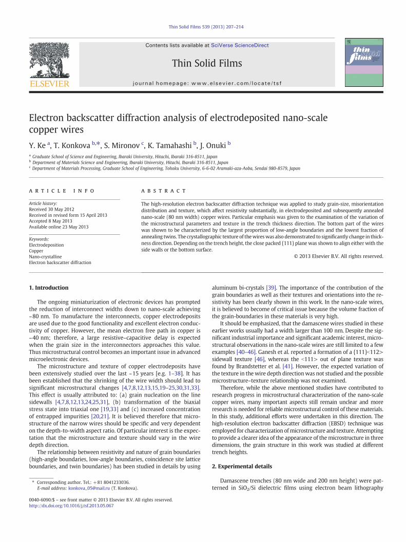
and reactive ion etching. An ultra-thin TaN/Ta (7.5 nm/7.5 nm) layerwas first sputter-deposited on the trenches as a diffusion barrier andadhesion layer, followed by sputter deposition of a 50 nm copper seedlayer to serve as the cathode for electroplating. Fig. 1 is a schematicdrawing of the trench structure. The reference directions employedwere denoted as longitudinal direction (LD), transversal direction (TD)and normal direction (ND).
The copper interconnectors were made by a normal direct currentelectroplating process at room temperature and a current density of5 mA/cm2. In order to eliminate impurities, a high purity of 99.999999%(8N) copper anode and 99.9999% (6N) CuSO4·5H2O copper electrolytewere used. Organic additives were also added to the solution to enhancethe filling capability of copper. The total plating time was 162 s, and thethickness of the electroplated layer was 300 nm. After completion ofthe electrodeposition process, the obtained samples were immediatelywashed with distilled water and dried with argon gas.
Due to lattice distortion and the finenature of themicrostructure, re-liable EBSDmaps could not be obtained from the as-deposited material.For this reason, the obtainedmaterial was annealed at 573 K for 10 minin vacuum (6.6 × 10⁻³ Pa) without delay after electrodeposition. Itshould be noted that the annealing treatment was performed withoutremoval of the excess copper layer (so-called, overburden layer).
All microstructural observations were made on the longitudinal(i.e. LD-TD) plane. After completion of the anneal treatment, chemicalmechanical polishing was applied to remove the excess copper andTaN/Ta layers from the trenchers as well as to get the EBSD final sur-face finish. To evaluate the possible variations of microstructure andtexture in the thickness direction, the observations were made atthe trench heights of 50, 100 and 200 nm, which correspond to bot-tom, mid-thickness and upper parts of the deposits, respectively.
The high-resolution EBSD analysis was performed with a HitachiS-4300SE field emission gun scanning electron microscope equippedwith a TSL OIM™ EBSD system. A triangular scanning grid wasemployed for orientation mapping. The EBSD maps were acquiredwith a scan step size of 30 nm. Due to limited experimental accuracyof EBSD, a lower limit boundary misorientation cut-off of 2° was used.A 15° criterion was used to differentiate low-angle boundaries (LABs)and high-angle boundaries (HABs).
3. Results and discussion
3.1. Preprocessing of EBSD data
The nano-scale electrodeposited copper wire is not a trivial objectfor EBSD measurements. In this regard, some details of the EBSD data
Fig. 1. Schematic representation with a superimposed reference frame of a trench crosssection before electroplating. See Section 2 for details.
preprocessing procedure are briefly considered in this section. Thisissue has never been analyzed in details before.
The acquired EBSD maps included data pixels obtained from thecopper wires as well as from the inter-trench space, as exemplified inFig. 2(a). For adequate EBSD analysis, therefore, it was necessary to ex-tract the copper data from the global data set. This was done by usingthe image quality (IQ) index. In EBSD, this index quantifies sharpnessof the Kikuchi patterns and therefore it is closely linkedwith perfectionof the crystal structure. The inter-trench space (black areas in Fig. 2(a))had an amorphous structure and thus a low IQ index. The distribution ofthe IQ indexes shown in Fig. 2(b)was distinctly bimodalwith peaks cor-responding to the inter-trench space and the copperwire. This providesan opportunity for easy data separation by selection of an appropriatethreshold IQ value (~70 in Fig. 2). The procedure for IQ-filtering is illus-trated by Fig. 3(a) and (b).
After this procedure, however, the EBSD data were still contaminat-ed by sporadic pixels having random crystal orientation. These are typ-ically located at grain boundaries or wire edges (an example is markedwith a red arrow in Fig. 3(b)). In EBSD, these pixels are usually attribut-ed to overlapping of Kikuchi patterns from neighboring grains orphases. In the considered case, some of these data points might alsobe surviving pixels belonging to the inter-trench space. To removethem from the EBSD maps, a standard grain dilation option of the TSLsoftware was used. According to this option, all small grains comprisingless than 3 pixels were eliminated from the EBSD data set. The finallyobtained EBSD map is shown in Fig. 3(c). Such maps were used in thepresent study for microstructural analysis. The described preprocessingprocedure was, in fact, performed in the inverse order, i.e. the grain di-lation was first and the IQ-filtering was second.
3.2. Structure morphology and grain size as a function of trench height
The grain boundary maps illustrating the microstructure at threedifferent trench heights are summarized in Fig. 4. Ignoring twins,the copper wires were only one grain in width and the HABs typicallyhad transverse orientation. The grain structure of the wires, therefore,was like bamboo. Taking into account that the wire width was 80 nm,the underlying grain structure was nanocrystalline in nature at leastin one (i.e. the width) dimension.
The grains contained a developed LAB substructure which wasmore pronounced in the bottom part of the trench (Fig. 4(a)). TheLABs were either transverse in nature or arranged as loose cells (anexample is marked with the gray arrow in Fig. 4(a)). The latter onesusually had very low (~2–3°) misorientation. The mechanism forthe LAB formation in the deposited material is not clear. One possibleexplanation has been proposed by Read et al. [47]. According to theirconcept, some copper atoms may cluster in the electroplating solu-tion as their travel to the cathode. Agglomeration of these clustersin the final deposit may give rise to the LAB substructure.
Another important feature of the deposited grain structure was sig-nificant fraction of twin boundaries. The twins are often found in thecopper electrodeposits but their origin is still not completely clear.They may develop during electrodeposition itself [48] as well as duringsubsequent annealing.While the formation of annealing twins in copperis well established [49], themechanism of twinning during electrodepo-sition is less clear. One of the possible explanations for this phenomenonis the presence of crystal growth faults induced by impurities [50].
The grain and sub-grain size distributions measured at differentheights of the trenches are summarized in Fig. 5(a) and (b). In allcases, the grain (or sub-grain) areas in an EBSD map were measuredand the equivalent grain diameters were calculated assuming eachgrain to be a circle (grain reconstruction method [51]). To avoid anypossible misunderstanding, the terms “grain” and “sub-grain” areused here to refer to the crystallites bordered by a continuous bound-ary having a misorientation of greater than 15° and 2°, respectively.

Fig. 2. (a) Selected portion of a typical image quality map and (b) the respective image quality distribution. See Section 3.1 for details.
209Y. Ke et al. / Thin Solid Films 539 (2013) 207–214
The grain size distributionswere broadly similar to each other beingsingle-modal and centering near ~150 nm (Fig. 5(a)). On the otherhand, the sub-grain sizeswere not homogeneous in the thickness direc-tion; the smallest was at the bottom part of the trench (Fig. 5(b)). In allcases, however, the volume fraction of the grains and sub-grains withsizes smaller than 40–50 nm was negligibly small.
The grain reconstruction method enables volume fraction of grainsof different sizes to be evaluated and this approach is particularly usefulfor evaluation of the relationship between structure and properties. Onthe other hand, the grains in the studied material were not equiaxed(Fig. 4) and therefore the grain size measured by the grain reconstruc-tion method had no clear physical meaning. In this regard, grain length
Fig. 3. Inverse pole figure EBSD maps illustrating “cleaning” of EBSD data: (a) original data;given in the bottom right corner. See Section 3.1 for details.
and sub-grain length (i.e. the size in the LD) were also measured byusing the linear interceptmethod. The obtained results are summarizedin Fig. 6. The typical grain and sub-grain lengths were close to 100 nm;again the shortest was in the bottom part of the trench. Therefore thegrain size becomes smaller towards the bottom part of the trench. Thenumber fraction of the sub-grains shorter than the mean electron freepath (40–50 nm) was ~4%.
3.3. Texture as a function of trench height
The orientation data derived from the EBSD maps in Fig. 4 were ar-ranged as 111 and 110 pole figures and they are summarized in Fig. 7
(b) after IQ filtering; and (c) after the grain dilation procedure. A color code triangle is

Fig. 4. Grain boundary EBSD maps illustrating microstructure at different heights of the trenches: (a) 50 nm; (b) 100 nm; and (c) 200 nm. In the maps, LABs, HABs and Σ3 twinboundaries are depicted as green, black and red lines, respectively. The inter-trench spaces appear as black. See Section 3.2 for details.
210 Y. Ke et al. / Thin Solid Films 539 (2013) 207–214
as a function of the trench height. The pole figures have the adopted ref-erence frame, i.e. the LD is vertical and TD is horizontal. It is worth not-ing that the texture in the bottompart of the nano-scalewires has neverbeen studied before.
The textures developed at the trench mid-thickness and in its upperpart were broadly similar to each other. In these cases, the b111> direc-tionwas alignedwith the TD and thus the {111} plane was nearly paral-lel to the trench side walls. The formation of such texture has also beenextensively reported in the literature [e.g. 4,7,24,25,37,38] and mighteasily be explained in terms of the nucleation of the copper deposit atthe trench side walls. The texture evolved in the trench mid-thicknessand in its upper part was close to the fiber b111>//TD texture.
It is worth noting that the grain growth in the upper part of thecopper lines may often be affected by the downward penetration of
Fig. 5. Distributions of (a) grain size and (b) sub-grain size measured at different heig
the growing grains from overburden layer [1,28,40,41]. In this case,the formation of b100>− or b111> out of plane texture would beexpected in this region. However, this was not observed in the presentstudy, and therefore the influence of excess copper layer on the graingrowth behavior was thought to be insignificant.
In the bottom part of the trench, the grains were oriented suchthat b111> was nearly parallel to the ND and b110> to the LD(Fig. 7(a)). Thus the texture that evolved in the bottom part of thetrench was dominated by {111}b110> orientation. It is worth notingthat the alignment of the b110> direction with the wire axis wasmuch more pronounced than that in the trench mid-thickness andin its upper part (compare Fig. 7(a) and (b) and (c)). The alignmentof the close-packed {111} plane with the substrate surface is conven-tionally associated to the equilibration of the surface energy whereas
hts of trenches using the grain reconstruction method. See Section 3.2 for details.

Fig. 6. Distributions of (a) grain size and (b) sub-grain size measured at different heights of trenches using the linear intercept method. See Section 3.2 for details.
211Y. Ke et al. / Thin Solid Films 539 (2013) 207–214
the alignment of the b110>with the LDmay be attributed to the min-imization of strain energy [23].
Therefore, the observed texture might be described in terms of thealignment of the close packed {111} planes with the substrate surface.Depending on the trench height, the latter one was the side walls orthe bottom surface.
Fig. 7. 111 and 110 pole figures illustrating texture at three t
Taking into account the principal change of the texture in the depthdirection, it may be concluded that the height of the bottom grains wasless than 100 nm. These grains, therefore, were nano-scale in all threedimensions, i.e. in width, length and height.
It is also remarkable, that the measured texture was surprisinglystrong, being ~15 times more random (Fig. 7). This may also explain
rench heights: (a) 50 nm; (b) 100 nm; and (c) 200 nm.

Fig. 8. (a) Misorientation angle distributions and (b) deviation of measured twin misorientations from the ideal Σ3 relationship. See Section 3.4 for details.
212 Y. Ke et al. / Thin Solid Films 539 (2013) 207–214
the presence of the LABs in the depositedmaterial. If the orientation dif-ference of the neighboring nuclei is small they may converge thus pro-ducing a LAB.
3.4. Misorientation distribution as a function of trench height
The misorientation data derived from the EBSD maps in Fig. 4 werearranged as misorientation angle distributions and misorientation axisdistributions as a function of the trench depth in Figs. 8(a) and 9, re-spectively. The area fractions of coincident site lattice (CSL) boundariesare summarized in Table 1. The effect of the wire depth on themisorientation characteristics have never been studied in the nano-scale lines before.
The EBSD measurements revealed that all misorientation angledistributions were principally similar, being featured a pronouncedlow-angle maximum as well as a sharp peak near 60° (Fig. 8(a)).The oscillations seen in the intermediate angular range of the distri-butions were thought to be related with experimental scatteringcaused by limited statistics. The 60° peak as well as the dense clusterof the misorientation axes near the b111> pole (Fig. 9) were attribut-able to the significant fraction of Σ3 twin boundaries (Table 1).
To provide an insight into the nature of the twin boundaries, thedeviations of the measured misorientations of the twin boundariesfrom the ideal Σ3 were measured and the obtained results areshown in Fig. 8(b). It is seen that the deviations are small being typi-cally within the experimental EBSD error (Fig. 8(b)). This presumablyindicates that the twin boundaries have primarily originated from theannealing twinning. In copper, this phenomenon is usually observedduring recrystallization or grain growth.
In addition to theΣ3, themisorientation distributionswere also char-acterized by increased fractions of Σ7, Σ13b, Σ19b and Σ21a CSL bound-aries (Table 1). All these misorientations lie in the misorientation rangeof ~20–45°b111>. In face-centered cubic metals (including copper) theboundaries close to 40°b111> are well known to be highly mobile [49]and thus their area may rapidly increase during recrystallization. Itseems therefore from the misorientation data that the microstructure
Fig. 9. Misorientation axis distributions for three he
studied in this work was significantly influenced by the post-deposition annealing.
As mentioned in the previous section, the formation of a strongtexture may influence the misorientation of grain boundaries. In thepresent study the texture was found to be very sharp (Fig. 7) andtherefore a possible texture–misorientation relationship was exam-ined. To this end, high-angle parts of measured misorientation angledistributions were compared with texture-derived distributions. Incontrast to the measured distributions displaying the misorientationsbetween neighboring pixels in an EBSD map, the texture-derivedones were calculated assuming no spatial correlation between thepixels. In other words, all possible misorientations between the pixelssampled (including noncontiguous ones) were calculated. For thetrench heights of 100 and 200 nm, the EBSD data were combined to-gether in an attempt to improve experimental statistics. The obtainedmisorientation angle distributions are summarized in Fig. 10. Themeasured and texture-derived distributions were in a good agree-ment with the exception of the twin-related peak near 60°. This con-firms that the grain boundary distribution was indeed significantlyinfluenced by the texture.
The misorientation distributions at the trench mid-thickness andin its upper part were broadly similar to each other (Figs. 8 and 9,Table 1). The bottom region, however, was characterized by a largerLAB fraction, but smaller proportion of Σ3, Σ7, Σ13b, Σ19b and Σ21aboundaries (Fig. 8(a), Table 1). This may be evidence that the recrys-tallization and grain growth was relatively difficult in this area forsome reason.
4. Conclusions
In this work, the high-resolution EBSD technique was employed tostudy the microstructure developed in very narrow (80 nm width)nano-scale copper wires during electrodeposition and subsequentannealing. The grain-size, texture and misorientation-angle distribu-tions were studied as a function of trench depth. The main conclu-sions are as follows.
ights: (a) 50 nm; (b) 100 nm; and (c) 200 nm.

Table 1CSL misorientations.
CSL misorientation Area fraction, %
50 nm height 100 nm height 200 nm height
10.1 15.3 19.10.4 0.1 0.41.5 2.5 2.30.6 0.3 0.60.8 0.4 0.60 0.1 0.30.9 1.4 1.30.3 0.3 0.30 0 0.30.5 0.4 0.10.3 0.1 0.50.2 1.2 0.60.5 1.4 0.90.3 0 00.1 0 00.6 0.2 0.20.1 0.2 0.10.1 0.2 0.10 0.1 0.60.1 0 00.1 0.2 0
Σ3 60°<111>Σ5 36.87°<100>Σ7 38.21°<111>Σ9 38.94°<110>Σ11 50.48°<110>Σ13a 22.62°<100>Σ13b 27.79°<111>Σ15 48.19°<210>Σ17a 28.07°<100>Σ17b 61.73°<221>Σ19a 26.53°<110>Σ19b 46.83°<111>Σ21a 21.79°<111>Σ21b 44.42°<211>
Σ23 40.45°<311>Σ25a 16.26°<100>
Σ25b 51.68°<331>Σ27a 31.59°<110>Σ27b 35.43°<210>Σ29a 43.60°<100>Σ29b 46.40°<221>
Note: CSL misorientation area fractions which exceed 1% are highlighted with gray.
213Y. Ke et al. / Thin Solid Films 539 (2013) 207–214
1) Texture distribution was found to be essentially inhomogeneousin the wire depth direction. In the upper and mid-thickness ofthe wires, the material was characterized by the b111> sidewalltexture. In the bottom part, the {111}b110> out-of-plane texturepredominated. The observed effect was attributed to the differentmechanisms of grain nucleation during electro-deposition pro-cess. In all cases, the textures were relatively strong with thepeak intensity of 111 and 110 pole figures achieving ~15 timesmore random.
2) In contrast to the texture, grain structure did not principally alterin the depth direction. In all cases, the grains typically spannedacross the entire wire width thus producing a bamboo-like micro-structure. In all cases, the microstructure was characterized bysignificant proportion of twin boundaries and LABs. The mis-orientation across the twin boundaries was close to the ideal Σ3thus indicating that the twins most likely originated either fromrecrystallization or grain growth. The LABs were found to be fre-quently arranged as loose cells having very small misorientationand size. This observation was hypothesized to be related withclustering of copper atoms as their travel to the cathode duringthe electrodeposition process.
Fig. 10. Comparison of experimental and texture-derived misorientation distributions in thedetails.
3) The misorientation distribution was featured by a significant pro-portion of highly-mobile 40°b111> boundaries probably originat-ing from recrystallization. In addition to the recrystallization, theprocess of formation of grain-boundaries was demonstrated tobe significantly influenced by the texture.
4) The fractions of high-angle and twin boundaries notably decreasetowards the bottom part of the wire. This may be evidence thatthe recrystallization and grain growth was relatively difficult inthis area for some reason.
Acknowledgments
Financial support from Grants-in-aid for Science Research (Con-tract Nos. 17206071 and 20226014) and from JST is gratefully ac-knowledged. The authors are very grateful to Nippon & Metal Co.,Ltd. for supplying the high purity electroplating solution andultrahigh purity anode copper plate. They also would like to thankMr. T. Namekawa for technical assistance.
References
[1] C. Lingk, M.E. Gross, J. Appl. Phys. 84 (1998) 5547.[2] S.H. Brongersma, E. Richard, I. Vervoort, H. Bender, W. Vandervorst, S. Lagrange,
G. Beyer, K. Maex, J. Appl. Phys. 86 (1999) 3642.[3] J.M.E. Harper, C. Cabral Jr., P.C. Andricacos, L. Gignac, I.C. Noyan, K.P. Rodbell, C.K.
Hu, J. Appl. Phys. 86 (1999) 2516.[4] C. Lingk, M.E. Gross, W.L. Brown, Appl. Phys. Lett. 74 (1999) 682.[5] S. Lagrange, S.H. Brongersma, M. Judelewicz, A. Saerens, I. Vervoort, E. Richard, R.
Palmans, K. Maex, Microelectron. Eng. 50 (2000) 449.[6] C. Lingk, M.E. Gross, W.L. Brown, J. Appl. Phys. 87 (2000) 2232.[7] D.F. Field, D. Dornisch, H.H. Tong, Scripta Mater. 45 (2001) 1069.[8] P.R. Besser, E. Zschech, W. Blum, D. Winter, R. Ortega, S. Rose, M. Herrick, M. Gall,
S. Thrasher, M. Tiner, B. Baker, G. Braeckelmann, L. Zhao, C. Simpson, C. Capasso,H. Kawasaki, E. Weitzman, J. Electron. Mater. 30 (2001) 320.
[9] S.H. Brongersma, E. Kerr, I. Vervoort, A. Saerens, K. Maex, J. Mater. Res. 17 (2002)582.
[10] M.-S. Yoon, Y.-J. Park, Y.-C. Joo, Thin Solid Films 408 (2002) 230.[11] D.P. Field, O.V. Kononenko, V.N. Matveev, J. Electron. Mater. 31 (2002) 40.[12] J.-K. Jung, N.-M. Hwang, Y.-C. Joo, J. Korean Phys. Soc. 40 (2002) 90.[13] D.P. Field, T. Muppidi, J.E. Sanchez, Scanning 25 (2003) 309.[14] J.-M. Paik, Y.-J. Park, M.-S. Yoon, J.-H. Lee, Y.-C. Joo, Scr. Mater. 48 (2003) 683.[15] W. Wu, D. Ernur, S.H. Brongersma, M. Van Hove, K. Maex, Microelectron. Eng. 76
(2004) 190.[16] J.-M. Paik, K.-C. Park, Y.-C. Joo, J. Electron. Mater. 33 (2004) 48.[17] H. Park, S.-J. Hwang, Y.-C. Joo, Acta Mater. 52 (2004) 2435.[18] J.-K. Jung, N.-M. Hwang, Y.-J. Park, Y.-C. Joo, Jpn. J. Appl. Phys. 43 (2004) 3346.[19] T. Muppidi, D.P. Field, J.E. Sanchez Jr., C. Woo, Thin Solid Films 471 (2005) 63.[20] W. Zhang, S.H. Brongersma, T. Conard, W. Wu, M. Van Hove, W. Vandervorst, K.
Maex, Electrochem. Solid-State Lett. 8 (2005) C95.[21] W. Zhang, S.H. Brongersma, N. Heylen, G. Beyer, W. Vandervorst, K. Maexa,
J. Electrochem. Soc. 152 (2005) C832.[22] J.-K. Jung, N.-M. Hwang, Y.-J. Park, Y.-C. Joo, J. Electron. Mater. 34 (2005) 559.[23] J.-Y. Cho, K. Mirpuri, D.N. Lee, J.-K. An, J.A. Szpunar, J. Electron. Mater. 34 (2005)
53.
HAB range for two trench heights: (a) 50 nm and (b) 100–200 nm. See Section 3.4 for

214 Y. Ke et al. / Thin Solid Films 539 (2013) 207–214
[24] J.-Y. Cho, H.-J. Lee, H. Kim, J.A. Szpunar, Arch. Metall. Mater. 50 (2005) 261.[25] J.-Y. Cho, H.-J. Lee, H. Kim, J.A. Szpunar, J. Electron. Mater. 34 (2005) 506.[26] N.-J. Park, D.P. Field, M.M. Nowell, P.R. Besser, J. Electron. Mater. 34 (2005) 1500.[27] K.J. MIirpur, J.A. Szpunar, J. Electron. Mater. 34 (2005) 1509.[28] H.J. Lee, H.N. Han, D.N. Lee, J. Electron. Mater. 34 (2005) 1493.[29] N.-J. Park, D.P. Field, Scr. Mater. 54 (2006) 999.[30] J.-M. Paik, I.-M. Park, Y.-C. Joo, Ki-Chul Park, J. Appl. Phys. 99 (2006) 024509.[31] K. Vanstreelsa, S.H. Brongersmam, Zs. Tokei, L. Carbonell, W. De Ceuninck,
J. D'Haen, M. D'Olieslaeger, J. Mater. Res. 23 (2008) 642.[32] S.-J. Hwang, Y.-C. Joo, J. Koike, Thin Solid Films 516 (2008) 7588.[33] C.-J. Chung, D.P. Field, N.-J. Park, R.G. Johnson, Thin Solid Films 517 (2009) 1977.[34] C.K. Yoon, D.P. Field, J. Electron. Mater. 39 (2010) 191.[35] A.S. Budiman, H.-A.-S. Shin, B.-J. Kim, S.-H. Hwang, H.-Y. Son, M.-S. Suh, Q.-H.
Chung, K.-Y. Byun, N. Tamura, M. Kunz, Y.-C. Joo, Microelectron. Reliab. 52(2012) 530.
[36] H.-S. Shin, B.-J. Kim, J.-H. Kim, S.-H. Hwang, A.S. Budiman, H.-Y. Son, K.-Y. Byun, N.Tamura, M. Kunz, D.-I. Kim, Y.-C. Joo, J. Electron. Mater. 41 (2012) 712.
[37] M.E. Gross, C. Lingk, W.L. Brown, R. Drese, Solid State Technol. 42 (1999) 47.[38] J.M. Paik, Y.-C. Joo, Mater. Sci. Forum 408–412 (2002) 1555.
[39] Nakamichi, Mater. Sci. Forum 207–209 (1996) 47.[40] S. Brandsetter, V. Carreau, S. Maitrejean, M. Verdier, M. Legros, Microelectron.
Eng. 87 (2010) 383.[41] S. Brandsetter, E.F. Rauch, V. Carreau, S. Maitrejean, M. Verdier, M. Legros, Scr.
Mater. 63 (2010) 965.[42] J. Onuki, K. Khoo, Y. Sasajima, Y. Chonan, T. Kimura, J. Appl. Phys. 108 (2010), (Art.
No. 044302 2010).[43] K. Khoo, J. Onuki, Thin Solid Films 518 (2010) 3413.[44] J. Onuki, S. Tashiro, K. Khoo, N. Ishikawa, T. Kimura, Y. Chonan, H. Akahoshi,
J. Electrochem. Soc. 157 (2010) 857.[45] T. Inami, J. Onuki, M. Isshiki, Electrochem. Solid-State Lett. 14 (5) (2011) 1.[46] K.J. Ganesh, A.D. Darbal, S. Rajasekhara, G.S. Rohrer, K. Barmak, P.J. Ferreira, Nano-
technology 23 (2012) 1.[47] D.T. Read, Y.W. Cheng, R. Geiss, Microelectron. Eng. 75 (2004) 63.[48] S.C. Barnes, Acta Metall. 7 (1959) 700.[49] F.J. Humphreys, M. Hatherly, Recrystallization and Related Phenomena, Elsevier,
2004, (574 pp.).[50] T.B. Vaughan, Electrochim. Acta 4 (1961) 72.[51] F.J. Humphreys, J. Microsc. 195 (1999) 170.
Related Documents