Electrodeposition of CdTe on Stainless Steel 304 substrates By Patrick Rutto Submitted in Partial Fulfillment of the Requirements for the Degree of Master of Science in the Chemistry Program YOUNGSTOWN STATE UNIVERSITY May, 2018

Welcome message from author
This document is posted to help you gain knowledge. Please leave a comment to let me know what you think about it! Share it to your friends and learn new things together.
Transcript

Electrodeposition of CdTe on Stainless Steel 304 substrates
By Patrick Rutto
Submitted in Partial Fulfillment of the Requirements
for the Degree of
Master of Science
in the
Chemistry
Program
YOUNGSTOWN STATE UNIVERSITY
May, 2018

Electrodeposition of CdTe on Stainless Steel 304 Substrates
Patrick Rutto
I hereby release this thesis to the public. I understand that this thesis will be made available from the OhioLINK ETD Center and the Maag Library Circulation Desk for public access. I also authorize the University or other individuals to make copies of this thesis as needed for scholarly research. Signature: Patrick Rutto, Student Date Approvals: Dr. Clovis A. Linkous, Thesis Advisor Date Dr. Timothy Wagner, Committee Member Date Dr. Tom N. Oder, Committee Member Date Dr. Salvatore A. Sanders, Dean of Graduate Studies Date

iii
ABSTRACT
The energy we get from the sun is a key factor in electric power production on earth and
in space applications. The development of photovoltaic cells has enabled a new direct
method for solar electricity. However, the manufacturing cost of photovoltaic cells must
be lowered to have widespread implementation. Among the leading candidates CdTe, is
used for photovoltaic applications, since it has optimum band gap energy for the efficient
conversion of solar energy into electricity. It is produced by a series of vacuum
procedures, which is a significant part of its fabrication cost. In this work, cadmium
telluride (CdTe) thin films were electrodeposited on stainless steel 304 substrates using a
three-electrode system at a negative potential. Cadmium sulfate and tellurium dioxide in
pH 1.8 H2SO4 were used as the cadmium and tellurium sources, respectively. Deposition
conditions were adjusted to codeposit Cd and Te at the same rate. Films were deposited
on stainless steel 304 as a relatively inexpensive substrate. However, to obtain a proper
ohmic contact between CdTe and the steel, it was necessary to electrodeposit a thin
interlayer of pure Te to achieve an ohmic contact. Electrodeposition of a thin Pt layer on
top of the CdTe served to greatly increase the rate of H2 evolution. The structural and
morphological properties of the resulting films were characterized using light/dark
voltammetric methods, X-ray diffraction (XRD), Profilometry, Scanning Electron
Microscopy (SEM) and Energy Dispersive Spectroscopy (EDS).

iv
ACKNOWLEDGEMENT
I would like to acknowledge the help of several individuals who have assisted me in
various aspects of this thesis and the work relating to it. Foremost, I would like to express
my sincere gratitude to my advisor Dr. Clovis A. Linkous for the continuous support of
my study and research, for his patience, motivation, enthusiasm, and immense
knowledge. Thank you so much for supervising the research which has led up to this
document and for the countless candies which were provided through regular visits to his
office. I would also like to thank Dr. Oder for the time, supervision, and direction he has
given to the research behind this thesis as well as the thesis itself. Dr. Timothy Wagner
thanks for guiding me in many of the improvements that have been made to this
document. I would also like to thank Ray for his help with the instruments. Of course; I
would like to thank my parents for their support too. A special thanks to fellow students
Solita, Milica, Seon, Linda and Omweri without whom nothing practical would have
gotten done. I am deeply grateful to my friends too for their support throughout my
research.

v
TABLE OF CONTENTS
ABSTRACT .................................................................................................................................... iii
ACKNOWLEDGEMENT .............................................................................................................. iv
TABLE OF FIGURES ................................................................................................................... vii
Chapter 1 .......................................................................................................................................... 1
1.1 INTRODUCTION ..................................................................................................................... 1
1.2 Solid state CdTe PV cell ............................................................................................................ 4
1.3 Review of Literature .................................................................................................................. 5
1.4 CdTe fabrication methods .......................................................................................................... 7
1.5 The Pourbaix diagram of CdTe- H2O system. ........................................................................... 9
Chapter 2 ........................................................................................................................................ 11
2.1 Objectives ................................................................................................................................ 11
2.2 Hypothesis ............................................................................................................................... 12
2.3 Electrodeposition ..................................................................................................................... 12
2.4 Photoelectrochemistry .............................................................................................................. 13
Conduction Band ................................................................................................................... 14
Valence band .......................................................................................................................... 14
Band gap ................................................................................................................................ 15
2.5 Significance of the study .......................................................................................................... 16
Chapter 3 ........................................................................................................................................ 17
3.1 Materials and experimental methods ....................................................................................... 17
3.2 Cyclic voltammetry .................................................................................................................. 23
3.3 Xenon Lamp ............................................................................................................................ 24

vi
3.4 Powder X-Ray diffraction ........................................................................................................ 26
3.5 Scanning electron microscopy (SEM) ..................................................................................... 27
Working principle of SEM ..................................................................................................... 27
3.6 Profilometer ............................................................................................................................. 28
Working principle of profilometer ......................................................................................... 29
3.7 Photoluminescence experiment ............................................................................................... 29
Chapter 4 ........................................................................................................................................ 30
4.1 Results and discussion ............................................................................................................. 30
4.1 Electrodeposition trials ............................................................................................................ 37
4.2 Scanning Electron Microscopy Studies ................................................................................... 41
4.3 Powder X-Ray Diffraction (PXRD) ......................................................................................... 53
4.4 Film thickness/profilometry ..................................................................................................... 54
Chapter 5 ........................................................................................................................................ 55
5.1 Conclusion and future work ..................................................................................................... 55
References ...................................................................................................................................... 57
vii
TABLE OF FIGURES
Figure 1: Illustration of some of potential renewable energy ............................................. 1
Figure 2: Schematic diagram showing electrode liquid junction Schottky barrier ............. 5
Figure 3: Atomic structure of CdTe .................................................................................... 7
Figure 4: Schematic diagram showing basic regions in Pourbaix diagram. ....................... 9
Figure 5: Equilibrium potential–pH (Pourbaix) diagram of the CdTe–H2O system ........ 10
Figure 6: Schematic diagram showing our proposed electrode ........................................ 11
Figure 7: Schematic diagram of a photoelectrochemical. ................................................. 14
Figure 8: Schematic diagram showing bands in a semiconductor. ................................... 15
Figure 9: Image of a three-electrode setup cell. ................................................................ 19
Figure 10: Schematic diagram showing steps on how to make SS304 electrode ............. 22
Figure 11: Stainless Steel 304 electrodes .......................................................................... 22
Figure 12: Setup experiment for electrodeposition ........................................................... 24
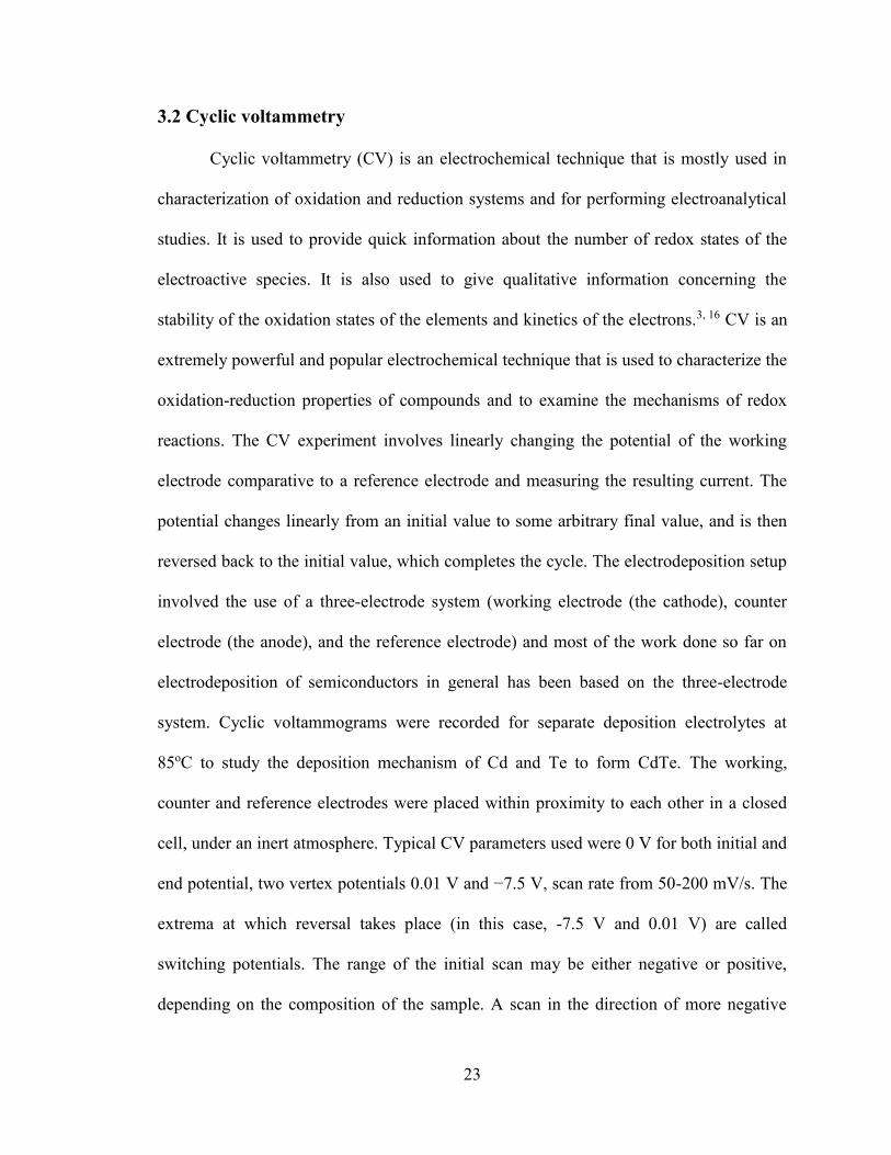
Figure 13: Cyclic voltammogram of CdTe under Xenon lamp ........................................ 25
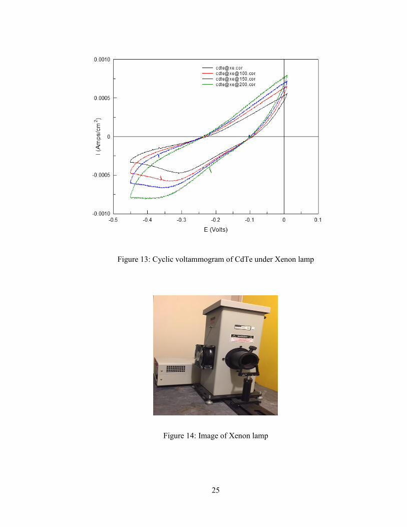
Figure 14: Image of Xenon lamp ...................................................................................... 25
Figure 15: Image of Powder XRD .................................................................................... 26
Figure 16: Schematic diagram of profilometer ................................................................. 28
Figure 17: Cyclic voltammogram for 0.5 M CdSO4. 50 mV/s sweep rate, SS 304
electrode, Ag/AgCl reference electrode, pH 1.8 H2SO4, under argon gas. ....................... 30
Figure 18: Cyclic voltammogram for Te (1×10⁻⁴ TeO2 in pH 1.8 H2SO4 on SS 304
electrode, Ag/AgCl reference electrode at 80 ºC, 85 ºC and 90 ºC scan rate 50 mV/s
respectively) ...................................................................................................................... 31
viii
Figure 19: Cyclic voltammogram of Te (-0.455V, 0.01V; at 80 ºC, 85 ºC and 90 ºC; scan
rate 50 mV/s)..................................................................................................................... 32
Figure 20: Temperature dependence cyclic voltammogram of CdTe deposition on bare
SS 304, 0.5 M CdSO4, 1×10⁻⁴ TeO2 in pH 1.8 H2SO4 (-0.455V, 0.01V; at 80 ºC, 85 ºC
and 90 ºC; scan rate 50 mV/s) ........................................................................................... 33
Figure 21: Cyclic voltammogram of CdTe deposition onto a Te/stainless steel 304
substrate 0.5 M CdSO4, 1×10⁻⁴ M TeO2, pH 1.8 H2SO4, Ar atmosphere’ Ag/AgCl
reference electrode at (80 ºC, 85 ºC and 90 ºC; scan rate 50 mV/s ). ............................... 34
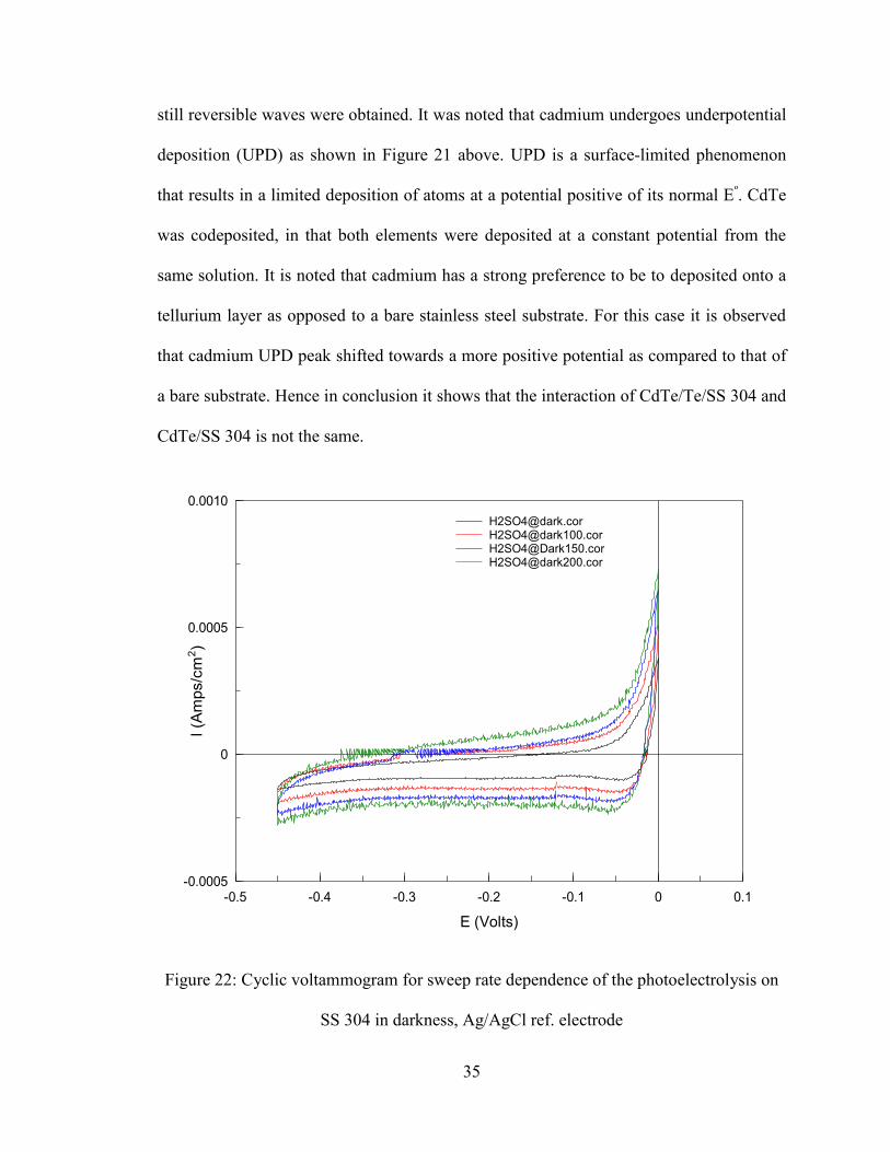
Figure 22: Cyclic voltammogram for sweep rate dependence of the photoelectrolysis on
SS 304 in darkness, Ag/AgCl ref. electrode……………………………………………..35
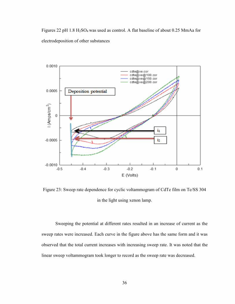
Figure 23: Sweep rate dependence for cyclic voltammogram of CdTe film on Te/SS 304
in the light using xenon lamp…………………………………………………………...36
Figure 24: Electrodeposition of Te at 80º C, for 480 s………………………………….37
Figure 25: Electrodeposition of CdTe on at 25º C, -0.45 V applied potential…………..38
Figure 26: Electrodeposition of CdTe at 80º C, -0.45 V………………………………...39
Figure 27: Effect of Pt deposition on CdTe/Te/SS304 at 80º C, -0.45 V………………..39
Figure 28: Cyclic voltammetry of Pt/CdTe/Te/SS 304…………………………………..39
Figure 29: SEM images of Cd film developed by electrodeposition ((a) 1000× and (b) 50
× respectively) ............................................................................................................... 42
Figure 30: SEM images of Te film developed by electrodeposition ((a) 50×and (b) 500×
respectively) ...................................................................................................................... 42
Figure 31: SEM images of unannealed CdTe film developed by electrodeposition ((a)
500×and (b) 1000× respectively ....................................................................................... 43

ix
Figure 32: SEM image of unannealed CdTe film electrodeposited under Ar (2500×). ... 43
Figure 33: SEM images of annealed CdTe film at 350oC (3500×, 3000× and 1400×
respectively) ...................................................................................................................... 44
Figure 34: EDX peaks and image showing elemental composition of unannealed CdTe at
2500× ................................................................................................................................ 45
Figure 35: EDX peaks and image showing elemental composition of annealed CdTe at
1000× ................................................................................................................................ 46
Figure 36: EDX image for blank SS 304 substrate at 1000× ............................................ 47
Figure 37: EDX image for unannealed CdTe powder scraped off of stainless steel 304
substrate at 1000× ............................................................................................................. 48
Figure 38: EDX image for annealed CdTe powder scraped off a stainless steel substrate at
(1000× magnification) ...................................................................................................... 49
Figure 39: PXRD image for CdTe deposited on SS 304 .................................................. 50
Figure 40: Spectrum of profilometer showing CdTe film thickness ................................ 51

1
Chapter 1
1.1 INTRODUCTION
The energy we receive from the sun is abundant and free from any pollutants.
This energy can be put into use as thermal, chemical, or electrical processes after
converting it. Northern Africa, the Middle East, and the United States of America are
known to have some of the richest resources of solar energy worldwide. For the past six
decades, consistent progress has been made in developing technologies to harness
electricity from solar radiation.1
Currently modern technology is being used to harness this energy for many
purposes such as generation of electricity, which can be used for heating water for
domestic, commercial, or industrial purposes. 1 Due to population growth and rise in
standards of living, the global energy demand is increasing rapidly. The illustration
shown below shows some of the potential renewable energy that can be used.
Figure 1: Illustration of some of potential renewable energy

2
In recent years, research towards sustainable and renewable energy has increased
significantly. Cadmium telluride (CdTe) photovoltaic cells work as a semiconductor that
converts energy of sunlight into DC (direct current) electricity. CdTe is an ideal absorber
material for high-efficiency low cost thin film polycrystalline solar cells. 2
Photovoltaic (PV) cells are important since they work as an integral part of solar-
electric energy systems, thus increasingly making them important as alternative sources
of utility power. Suitable semiconductors such as CdTe must therefore collect the
available photon energies, which are ideally equivalent to the band gap energy of the p-
type semiconductor.
The cadmium telluride semiconductor is well known as a stable photo-electrode,
with a band gap which is well suited to absorb most of solar spectrum. CdTe has a band
gap of 1.45eV, thus making it close to the ideal value for an efficient photovoltaic
conversion. High absorption of light from the sun and chemical stability are found for
CdTe. Thin film cadmium telluride (CdTe) is now regarded as a leading material for the
development of cost-effective photovoltaics.3
As compared to crystalline silicon, which was originally used to manufacture PV
cells, cadmium telluride is known to have several advantages. Thin CdTe films can be
made extremely thin, about a few micrometers, far thinner than a typical Si layer on order
of 100µm. Cadmium telluride is more efficient as compared to Si, especially at elevated
temperatures and low levels of illumination. Besides that, CdTe PV cells require less
energy for their production and due to its high optical absorption coefficient, the
compound is an attractive material for optoelectronics, gamma ray detector, and infrared

3
detector besides its PEC application. For this case, high quality growth of cadmium
telluride fine crystalline film is important because of its potential applications in
semiconducting devices, photovoltaic optoelectronic devices, radiation detectors, laser
materials, thermoelectric devices, solar energy converters, Videocon devices, sensors and
nano devices.4
Nevertheless, there are environmental concerns due to cadmium in CdTe PV
cells. Cadmium is a heavy metal that is known to be toxic, just like mercury and lead.
However, proponents of CdTe technology report that cadmium ion is insoluble in water,
so that Cd2+ should not pose any hazard to the groundwater. Furthermore, CdTe will not
vaporize in a fire. Cadmium is a harmful element, but once incorporated into PV
modules; its effects are reduced, so it does not cause a risk to the public.
A large number of deposition methods have been applied to CdTe, resulting in
high-quality films or layers leading to high-efficiency cells in economic production on
the other hand. Close spaced sublimation (CSS) is the most popular technique for
obtaining highest efficiencies; Spraying or screen printing are techniques with high
economic potential. It is remarkable that the highest efficiency CdTe PV devices are
fabricated from polycrystalline rather than single crystalline CdTe. A probable reason is
that grain boundaries enhance the collection of photogenerated minority carriers.5 In this
work, investigation of the electrode process of co-reduction of Cd2+ and HTeO2+ ions in
aqueous sulfuric acid was done to prepare cadmium telluride films by electrodeposition.
Characterization of cadmium telluride films electrodeposited on a stainless-steel substrate
was done by use of Scanning Electron Microscopy (SEM) and Energy Dispersive X-ray
(EDX) analysis.1

4
1.2 Solid state CdTe PV cell
One of the major challenges of CdTe solar cell research is the achievement of a
high hole density in the CdTe layer by means of controlled acceptor doping. CdTe grown
under Te rich conditions is mostly reported to be p-type and has a low resistivity. In this
case, from the research that has been performed, it is reported that utilizing a contact
material with the proper work function provides a low barrier height at the contact.
Heavy doping of the semiconductor adjacent to the contact promotes tunneling and adds
recombination centers to the semiconductor adjacent to the contact. Stainless steel 304 is
comprised of high percentage of iron, which is known to have a work function of 4.47eV.
One method of forming a tellurium contact is by electrodepositing it from a
solution containing Te ion. During tellurium layer formation, cadmium diffuses out of the
CdTe adjacent to the growing tellurium film, leaving CdTe with an excess of tellurium.
At the same time, tellurium may diffuse into this region aided by the cadmium vacancy
density, providing extrinsic p-type doping. This layer forms the actual contact or acts to
lower the barrier height. 11, 12
In general, as-prepared CdTe films fabricated by various techniques have high
electrical resistivity (107–109cm) and are slightly p-type doped due to the formation of
Cd vacancies in the CdTe lattice acting as acceptor centers.11, 22
In overall, photovoltaic cell is made up of a substrate, front contact, buffer layer,
absorber layer (p-type) and back contact. The substrate can be either metal, glass or
polymer foil. The substrate should be mechanically stable, have a matching thermal
expansion coefficient with the other deposited layers and be inert.
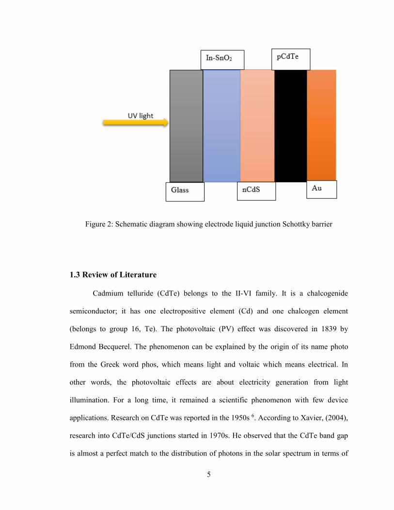
5
Figure 2: Schematic diagram showing electrode liquid junction Schottky barrier
1.3 Review of Literature
Cadmium telluride (CdTe) belongs to the II-VI family. It is a chalcogenide
semiconductor; it has one electropositive element (Cd) and one chalcogen element
(belongs to group 16, Te). The photovoltaic (PV) effect was discovered in 1839 by
Edmond Becquerel. The phenomenon can be explained by the origin of its name photo
from the Greek word phos, which means light and voltaic which means electrical. In
other words, the photovoltaic effects are about electricity generation from light
illumination. For a long time, it remained a scientific phenomenon with few device
applications. Research on CdTe was reported in the 1950s 6. According to Xavier, (2004),
research into CdTe/CdS junctions started in 1970s. He observed that the CdTe band gap
is almost a perfect match to the distribution of photons in the solar spectrum in terms of
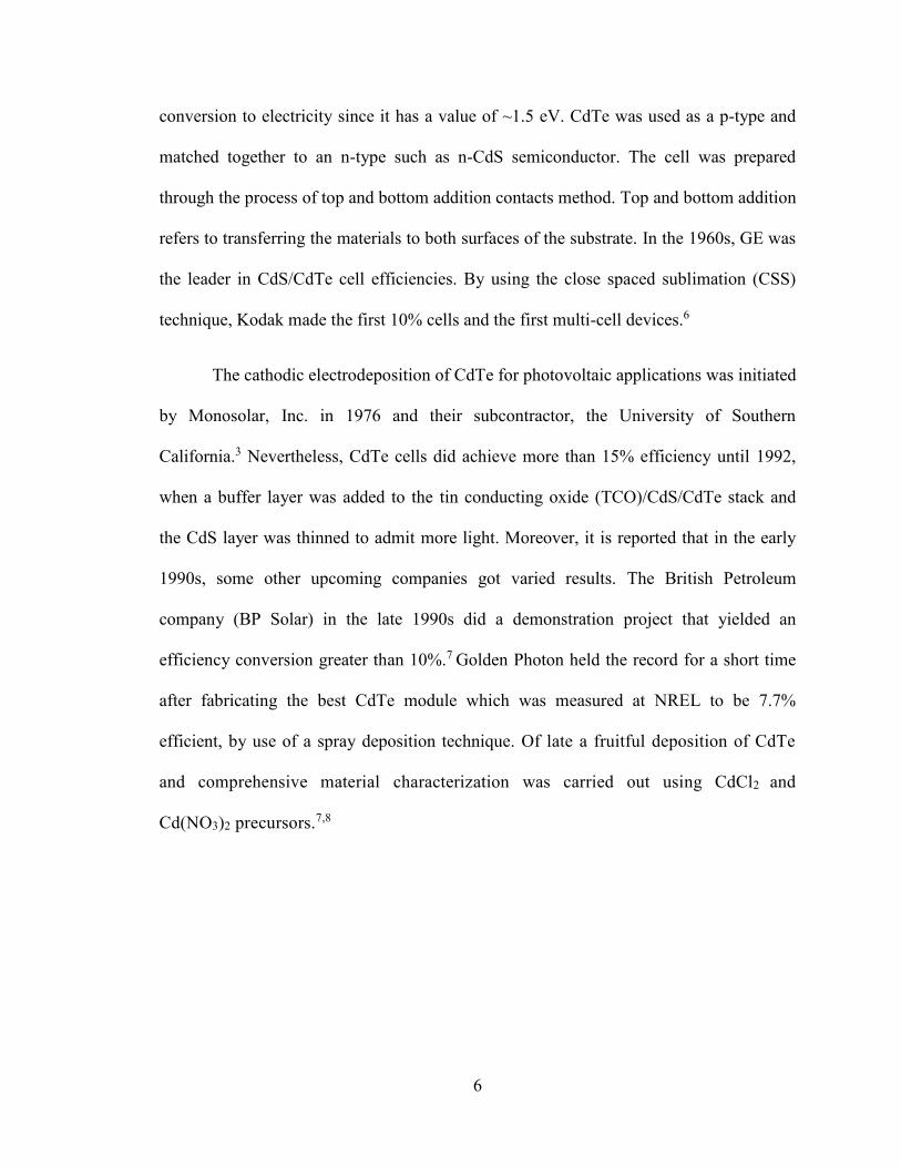
6
conversion to electricity since it has a value of ~1.5 eV. CdTe was used as a p-type and
matched together to an n-type such as n-CdS semiconductor. The cell was prepared
through the process of top and bottom addition contacts method. Top and bottom addition
refers to transferring the materials to both surfaces of the substrate. In the 1960s, GE was
the leader in CdS/CdTe cell efficiencies. By using the close spaced sublimation (CSS)
technique, Kodak made the first 10% cells and the first multi-cell devices.6
The cathodic electrodeposition of CdTe for photovoltaic applications was initiated
by Monosolar, Inc. in 1976 and their subcontractor, the University of Southern
California.3 Nevertheless, CdTe cells did achieve more than 15% efficiency until 1992,
when a buffer layer was added to the tin conducting oxide (TCO)/CdS/CdTe stack and
the CdS layer was thinned to admit more light. Moreover, it is reported that in the early
1990s, some other upcoming companies got varied results. The British Petroleum
company (BP Solar) in the late 1990s did a demonstration project that yielded an
efficiency conversion greater than 10%.7 Golden Photon held the record for a short time
after fabricating the best CdTe module which was measured at NREL to be 7.7%
efficient, by use of a spray deposition technique. Of late a fruitful deposition of CdTe
and comprehensive material characterization was carried out using CdCl2 and
Cd(NO3)2 precursors.7,8

7
Figure 3: Atomic structure of CdTe
1.4 CdTe fabrication methods
This study will involve the fabrication of electrodes. According to Dharmadasa, 9
preparations of semiconductor electrodes have been accomplished by a wide variety of
methods that include vapor deposition, spraying, screen printing, thermal evaporation,
electrodeposition, radio-frequency (rf) sputtering, electron beam evaporation, laser
ablation, sol-gel films and chemical bath techniques and closed space sublimation.
Thermal evaporation in vacuum is often used because it offers many possibilities to
modify the deposition conditions and study the effect of preparation conditions on the
physical properties of the respective films. It has been well established that in this
preparation method the process parameters like substrate temperature, source
temperature, and deposition frequency (rate) change the quality and physical properties of
the CdTe films.
The results of many research efforts have demonstrated that CSS is one of several
techniques with large area manufacturing potential due to its high throughput and
efficient material utilization.10
8
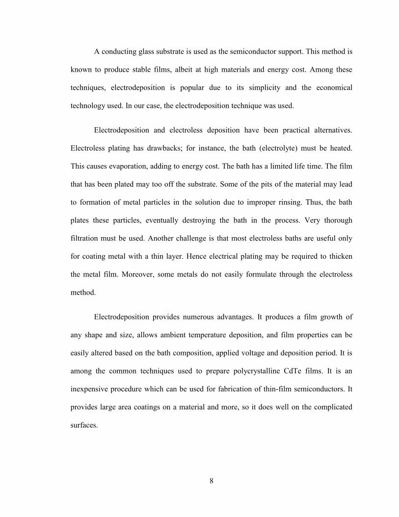
A conducting glass substrate is used as the semiconductor support. This method is
known to produce stable films, albeit at high materials and energy cost. Among these
techniques, electrodeposition is popular due to its simplicity and the economical
technology used. In our case, the electrodeposition technique was used.
Electrodeposition and electroless deposition have been practical alternatives.
Electroless plating has drawbacks; for instance, the bath (electrolyte) must be heated.
This causes evaporation, adding to energy cost. The bath has a limited life time. The film
that has been plated may too off the substrate. Some of the pits of the material may lead
to formation of metal particles in the solution due to improper rinsing. Thus, the bath
plates these particles, eventually destroying the bath in the process. Very thorough
filtration must be used. Another challenge is that most electroless baths are useful only
for coating metal with a thin layer. Hence electrical plating may be required to thicken
the metal film. Moreover, some metals do not easily formulate through the electroless
method.
Electrodeposition provides numerous advantages. It produces a film growth of
any shape and size, allows ambient temperature deposition, and film properties can be
easily altered based on the bath composition, applied voltage and deposition period. It is
among the common techniques used to prepare polycrystalline CdTe films. It is an
inexpensive procedure which can be used for fabrication of thin-film semiconductors. It
provides large area coatings on a material and more, so it does well on the complicated
surfaces.
9
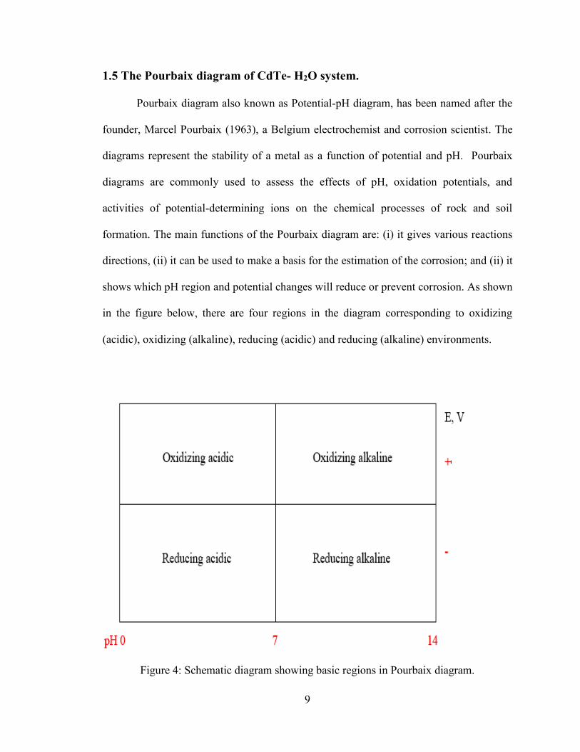
1.5 The Pourbaix diagram of CdTe- H2O system.
Pourbaix diagram also known as Potential-pH diagram, has been named after the
founder, Marcel Pourbaix (1963), a Belgium electrochemist and corrosion scientist. The
diagrams represent the stability of a metal as a function of potential and pH. Pourbaix
diagrams are commonly used to assess the effects of pH, oxidation potentials, and
activities of potential-determining ions on the chemical processes of rock and soil
formation. The main functions of the Pourbaix diagram are: (i) it gives various reactions
directions, (ii) it can be used to make a basis for the estimation of the corrosion; and (ii) it
shows which pH region and potential changes will reduce or prevent corrosion. As shown
in the figure below, there are four regions in the diagram corresponding to oxidizing
(acidic), oxidizing (alkaline), reducing (acidic) and reducing (alkaline) environments.
Figure 4: Schematic diagram showing basic regions in Pourbaix diagram.
10
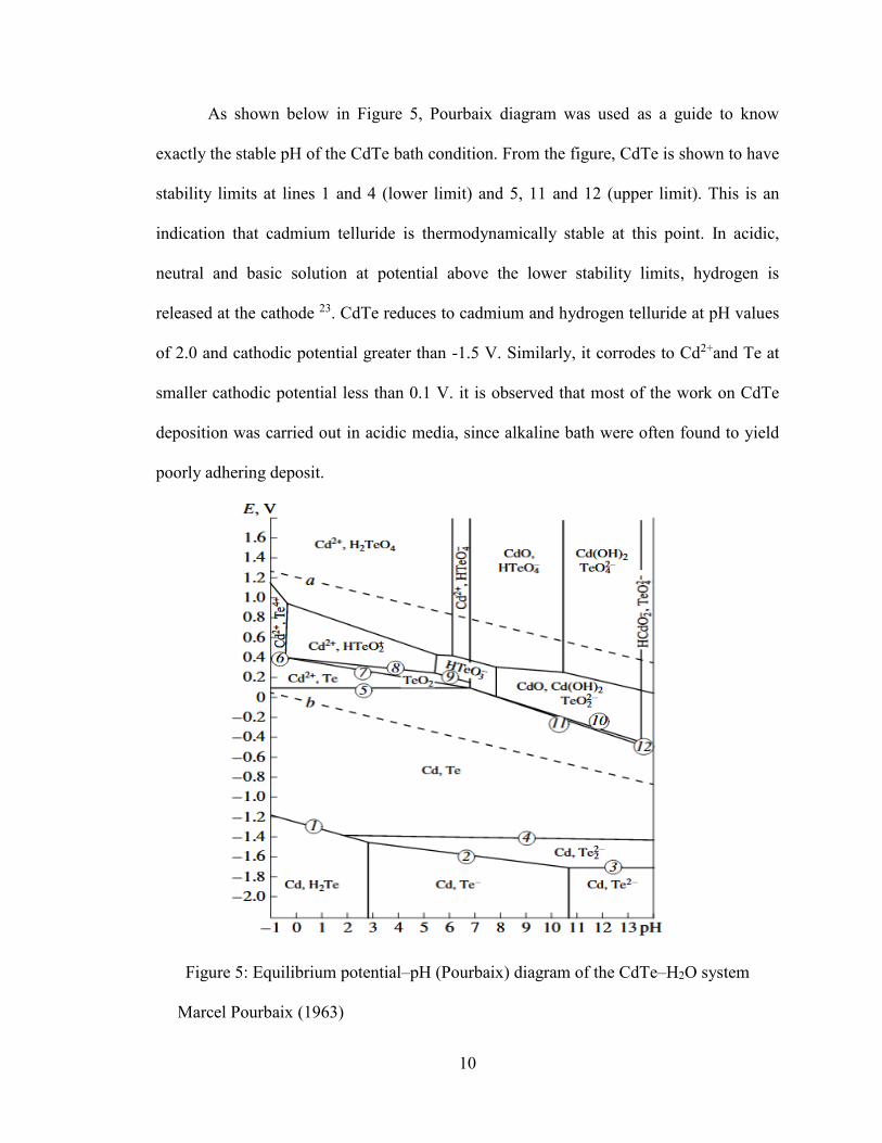
As shown below in Figure 5, Pourbaix diagram was used as a guide to know
exactly the stable pH of the CdTe bath condition. From the figure, CdTe is shown to have
stability limits at lines 1 and 4 (lower limit) and 5, 11 and 12 (upper limit). This is an
indication that cadmium telluride is thermodynamically stable at this point. In acidic,
neutral and basic solution at potential above the lower stability limits, hydrogen is
released at the cathode 23. CdTe reduces to cadmium and hydrogen telluride at pH values
of 2.0 and cathodic potential greater than -1.5 V. Similarly, it corrodes to Cd2+and Te at
smaller cathodic potential less than 0.1 V. it is observed that most of the work on CdTe
deposition was carried out in acidic media, since alkaline bath were often found to yield
poorly adhering deposit.
Figure 5: Equilibrium potential–pH (Pourbaix) diagram of the CdTe–H2O system
Marcel Pourbaix (1963)

11
Chapter 2
2.1 Objectives
1. To use electrodeposition method as a means of producing CdTe thin films on
stainless steel 304, brass and copper.
2. To apply them in a photoelectrochemical water-splitting scheme to produce hydrogen
using Xe lamp radiation as a source of simulated solar energy.
Figure 6: Schematic diagram showing our proposed electrode

12
2.2 Hypothesis
The pros and cons of semiconductors for energy generation are reviewed with
their operation principles and physical efficiency limits. The main materials currently
used or investigated and the associated fabrication methods for making CdTe are
described. Semiconductors fabricated from silicon dominate in terms of production as
compared to that of CdTe. Recent developments suggest that thin-film CdTe is a
promising candidate for future photovoltaics.
Our main purpose in this work is to develop low cost and efficient CdTe films
using stainless steel 304(SS 304) substrates, which will serve as photoelectrodes in a
photoelectrochemical cell, through which hydrogen is produced by photoelectrolytic
water splitting. This thesis is a continuation of Dr. Stephen Rhoden’s work, 5 and clearly
shows that modified electrodes must have more than enhanced kinetics. The intent is to
make thin films of CdTe on the stainless steel 304 substrates. This approach was
reported, 40 years ago by Honda and Fujishima.6 It involved the use of TiO2 as the
semiconductor electrode for water photolysis.
2.3 Electrodeposition
This is the deposition of a substance on an electrode by the action of an external
source (electricity). It is a technique that uses no vacuum and it gives good control over
the properties of the thin films through the influence of parameters such as deposition
potential, bath temperature, pH, and deposition time and electrolytes concentration. It is a
metal deposition process in which positively charged metal ions (M+) from the solution
are reduced and deposited on the surface of a negatively charged electrode (cathode) by
the passage of electric current. During electrodeposition, the substrate is immersed into
13
an aqueous solution, and polarized negative of the reduction potential, for this case
CdSO4 and TeO2, holding a temperature of around 80-90 °C.
2.4 Photoelectrochemistry
The electrodeposited CdTe on SS 304 substrate was used as the working electrode in
photo electrochemical cells. The counter electrode was a platinum foil or strip. The
principle of photoelectrochemical water splitting is based on light conversion into
electricity within a cell in which two electrodes immersed in a bath or electrolyte, of
which at least one is made of a semiconductor exposed to light and able to absorb light.
The resulting photovoltage is then used to drive water electrolysis. In the
photoelectrochemistry (PEC) of semiconductors, the electrochemical response of the
system is studied under the illumination of light. Incident photons generate electron-hole
pairs in the semiconductor. These energized electrons get excited to the conduction band
and corresponding holes are created in the valence band. Further movement and
recombination lifetime of the minority and the majority carriers depend on the type of
semiconductor and its physical properties.
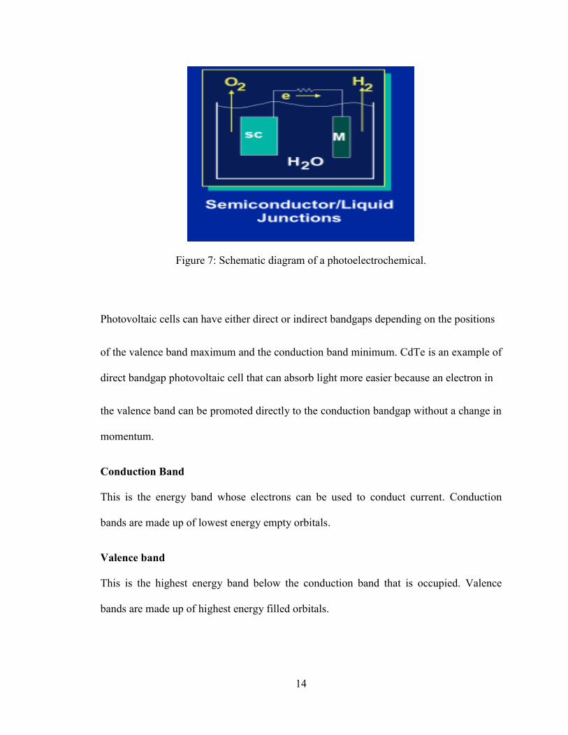
14
Figure 7: Schematic diagram of a photoelectrochemical.
Photovoltaic cells can have either direct or indirect bandgaps depending on the positions
of the valence band maximum and the conduction band minimum. CdTe is an example of
direct bandgap photovoltaic cell that can absorb light more easier because an electron in
the valence band can be promoted directly to the conduction bandgap without a change in
momentum.
Conduction Band
This is the energy band whose electrons can be used to conduct current. Conduction
bands are made up of lowest energy empty orbitals.
Valence band
This is the highest energy band below the conduction band that is occupied. Valence
bands are made up of highest energy filled orbitals.
15
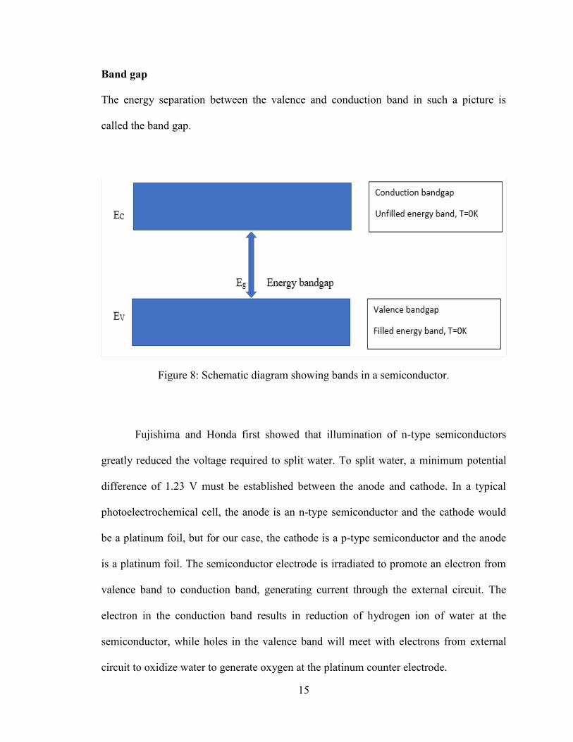
Band gap
The energy separation between the valence and conduction band in such a picture is
called the band gap.
Figure 8: Schematic diagram showing bands in a semiconductor.
Fujishima and Honda first showed that illumination of n-type semiconductors
greatly reduced the voltage required to split water. To split water, a minimum potential
difference of 1.23 V must be established between the anode and cathode. In a typical
photoelectrochemical cell, the anode is an n-type semiconductor and the cathode would
be a platinum foil, but for our case, the cathode is a p-type semiconductor and the anode
is a platinum foil. The semiconductor electrode is irradiated to promote an electron from
valence band to conduction band, generating current through the external circuit. The
electron in the conduction band results in reduction of hydrogen ion of water at the
semiconductor, while holes in the valence band will meet with electrons from external
circuit to oxidize water to generate oxygen at the platinum counter electrode.

16
Since previous research by Dr. Rhoden (2012) showed that the idea behind CdTe
is for redox chemistry to be performed on water, thus splitting it and providing hydrogen
gas for use as stored solar energy as shown by the equation:
2H2O 4H+ (aq) + 4e- + O2 (g) [E0 = -1.23 V]
4H+ (aq) + 4e- 2H2 (g) [E0 = 0.00 V]
Net: -1.23V
A semiconductor capable of spontaneous water splitting must have a conduction
band energy higher and a valence band energy lower than the reduction potential for
hydrogen ion to H2, Ered (H2/H+) and the oxidation potential for O2 evolution from water
Eox (OH-/O2), respectively. To drive the transfer of each electron in the process, the
semiconductor must supply an electro potential energy equivalent of at least 1.23 V. In
this work, the electrodeposition will be carried out in aqueous solution using a 3-
electrode potentiostated system.
2.5 Significance of the study
This study will be important to an analytical student because using CdTe PV cells to
split water and produce hydrogen has many applications:
For example, highly pure hydrogen can be obtained in requisite amounts which can be
used to store energy;
It can be useful in space shuttle and space missions.

17
It can be used in fuel cells and automobile applications.
Hydrogen is used in petroleum refining processes.
Chapter 3
3.1 Materials and experimental methods
Our research objective was to prepare suitable photovoltaic electrodes, which can
be assembled in a photochemical cell for hydrogen production by water splitting.
Equipment used for this experiment are Potentiostat (Model 273), hot plate, two wires
and alligator clips. All the chemicals and substrates used in this work were purchased
from Alfa Aesar and Fisher Chemicals. The anode and cathode clipped by an alligator
clip were then connected to a Potentiostat using a wire. The CdTe thin films were
potentiostatically electrodeposited on stainless steel 304 substrates using aqueous
solutions containing CdSO4 and TeO2 solution.
Solutions to be used for initial voltammetric studies were prepared using
deionized water to make different concentrations as follows:
0.01042g CdSO4 50ml 0.5 M CdSO4
0.007979g TeO2 50ml 1×10⁻⁴ M TeO2
0.2777ml concentrated H2SO4 50ml 1×10⁻² M H2SO4

18
For the sulfuric acid, 0.28 ml of concentrated stock solution was taken and diluted to
make a volume of 50 ml as shown above. This solution was used to adjust the pH to 1.8.
All lab equipment and some chemicals were already available in the laboratory.
The stainless steel 304 substrates obtained were cut to 2.6cm x 0.6cm rectangles before
any initial processing was performed. Trace metal grade hydrochloric acid (HCl), 99+ %
w/w cadmium sulfate (CdSO4), Chloroplatinic acid hexahydrate (H2PtCl6) and 99.99+%
tellurium oxide (TeO2) were obtained from Alfa Aesar. 96% w/w sulfuric acid (H2SO4)
was acquired from Fisher Scientific. For most of the work, deionized water was used for
rinsing, cleaning, and making all solutions. The solutions were kept for a day before
being used.
The stainless-steel squares were cleaned with detergent, followed by acetone,
methanol and then rinsed with deionized water and finally dried carefully. It was then
submerged and stirred in a 10% v/v HCl bath, followed by washing with deionized water
and consequent drying of surface by compressed argon gas. Deionized water was
generally used for cleaning, rinsing, and making solutions.
The electrolytes were prepared by dissolving cadmium and tellurium precursors in
acidified water. The electrodeposition of CdTe semiconductor thin films is effected
usually from aqueous acidic solutions. The concentrations varied from 1 mM to 0.5 M.
The precursors of Cd2+ and HTeO2+ ions were anhydrous CdSO4 and TeO2, respectively.
Semiconductor electrodeposition testing was done using a PAR 273A Potentiostat
in a conventional single compartment cell, with a three-electrode setup, consisting of a
stainless-steel 304 working electrode, a silver/silver chloride reference electrode (0.22V

19
vs NHE- Normal Hydrogen Electrode) and a platinum strip electrode (110 mm2 surface
area). The electrode at which the reaction of interest occurs is called working electrode.
For this case, in the three-electrode system, the potential of the working electrode was
measured relative to the reference electrode, which itself has a known and stable
electrode potential. Thus, the potential on the working electrode is precisely
controlled.7,11 This has the advantage of producing layers with controlled stoichiometry
since the effects of changes in certain deposition parameters such as stirring can be
minimized. Figure 9 below is a setup cell which was used in electrodeposition.
Figure 9: Image of a three-electrode setup cell.
20
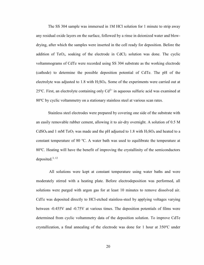
The SS 304 sample was immersed in 1M HCl solution for 1 minute to strip away
any residual oxide layers on the surface, followed by a rinse in deionized water and blow-
drying, after which the samples were inserted in the cell ready for deposition. Before the
addition of TeO2, soaking of the electrode in CdCl2 solution was done. The cyclic
voltammograms of CdTe were recorded using SS 304 substrate as the working electrode
(cathode) to determine the possible deposition potential of CdTe. The pH of the
electrolyte was adjusted to 1.8 with H2SO4. Some of the experiments were carried out at
25oC. First, an electrolyte containing only Cd2+ in aqueous sulfuric acid was examined at
80oC by cyclic voltammetry on a stationary stainless steel at various scan rates.
Stainless steel electrodes were prepared by covering one side of the substrate with
an easily removable rubber cement, allowing it to air-dry overnight. A solution of 0.5 M
CdSO4 and 1 mM TeO2 was made and the pH adjusted to 1.8 with H2SO4 and heated to a
constant temperature of 80 oC. A water bath was used to equilibrate the temperature at
80oC. Heating will have the benefit of improving the crystallinity of the semiconductors
deposited.3, 12
All solutions were kept at constant temperature using water baths and were
moderately stirred with a heating plate. Before electrodeposition was performed, all
solutions were purged with argon gas for at least 10 minutes to remove dissolved air.
CdTe was deposited directly to HCl-etched stainless-steel by applying voltages varying
between -0.455V and -0.75V at various times. The deposition potentials of films were
determined from cyclic voltammetry data of the deposition solution. To improve CdTe
crystallization, a final annealing of the electrode was done for 1 hour at 350oC under

21
argon atmosphere. The CdCl2 treatment at 350 °C in the presence of oxygen is known to
improve the cell efficiency.
The electrodes for photoelectrochemical testing were completed by attaching a
wire to the backside plate with silver epoxy, air-drying for 2 hours and finally covering
the entire attached electrode wire and backside with silicone. Photoelectrochemical
testing was done in stirred electrolytes, using a three-neck round bottom flask. The
cathodes were oriented vertically and had an exposed area of 2-4cm2, 12. A parallel Pt foil
was used as anode in the cell and electrolysis under controlled potential conditions was
conducted. Analytical electron microscopy images were taken using a JEOL JIB 4500
Focused Ion Beam/Scanning Electron Microscope (FIB/SEM) to show morphology with
an energy dispersive X-ray (EDX) detector for elemental analysis. Voltammograms were
obtained by performing cyclic voltammetry using the potentiostat. In the present
research, cyclic voltammetry was the primary technique.
22
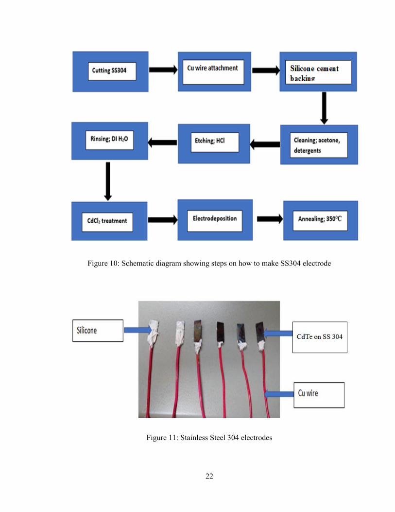
Figure 10: Schematic diagram showing steps on how to make SS304 electrode
Figure 11: Stainless Steel 304 electrodes
23
3.2 Cyclic voltammetry
Cyclic voltammetry (CV) is an electrochemical technique that is mostly used in
characterization of oxidation and reduction systems and for performing electroanalytical
studies. It is used to provide quick information about the number of redox states of the
electroactive species. It is also used to give qualitative information concerning the
stability of the oxidation states of the elements and kinetics of the electrons.3, 16 CV is an
extremely powerful and popular electrochemical technique that is used to characterize the
oxidation-reduction properties of compounds and to examine the mechanisms of redox
reactions. The CV experiment involves linearly changing the potential of the working
electrode comparative to a reference electrode and measuring the resulting current. The
potential changes linearly from an initial value to some arbitrary final value, and is then
reversed back to the initial value, which completes the cycle. The electrodeposition setup
involved the use of a three-electrode system (working electrode (the cathode), counter
electrode (the anode), and the reference electrode) and most of the work done so far on
electrodeposition of semiconductors in general has been based on the three-electrode
system. Cyclic voltammograms were recorded for separate deposition electrolytes at
85oC to study the deposition mechanism of Cd and Te to form CdTe. The working,
counter and reference electrodes were placed within proximity to each other in a closed
cell, under an inert atmosphere. Typical CV parameters used were 0 V for both initial and
end potential, two vertex potentials 0.01 V and −7.5 V, scan rate from 50-200 mV/s. The
extrema at which reversal takes place (in this case, -7.5 V and 0.01 V) are called
switching potentials. The range of the initial scan may be either negative or positive,
depending on the composition of the sample. A scan in the direction of more negative

24
potentials is termed a forward scan while one in the opposite direction is called a reverse
scan.
Figure 12: Setup experiment for electrodeposition
3.3 Xenon Lamp
A xenon arc lamp was used in this research as a source of simulated sunlight to
regenerate the adsorbent. It works as a lamp that discharge a gas, an electric light that
produces light by passing electricity through ionized xenon gas at high pressure. It gives
out a bright light that closely mimics natural light from the sun. figure 13 below shows
cyclic voltammogram of CdTe done at different sweep rates. Newport 500W and 1000W
xenon arc lamps were used in this work. Shown are voltammograms of CdTe obtained in
the dark and in the light by using a xenon lamp.
26
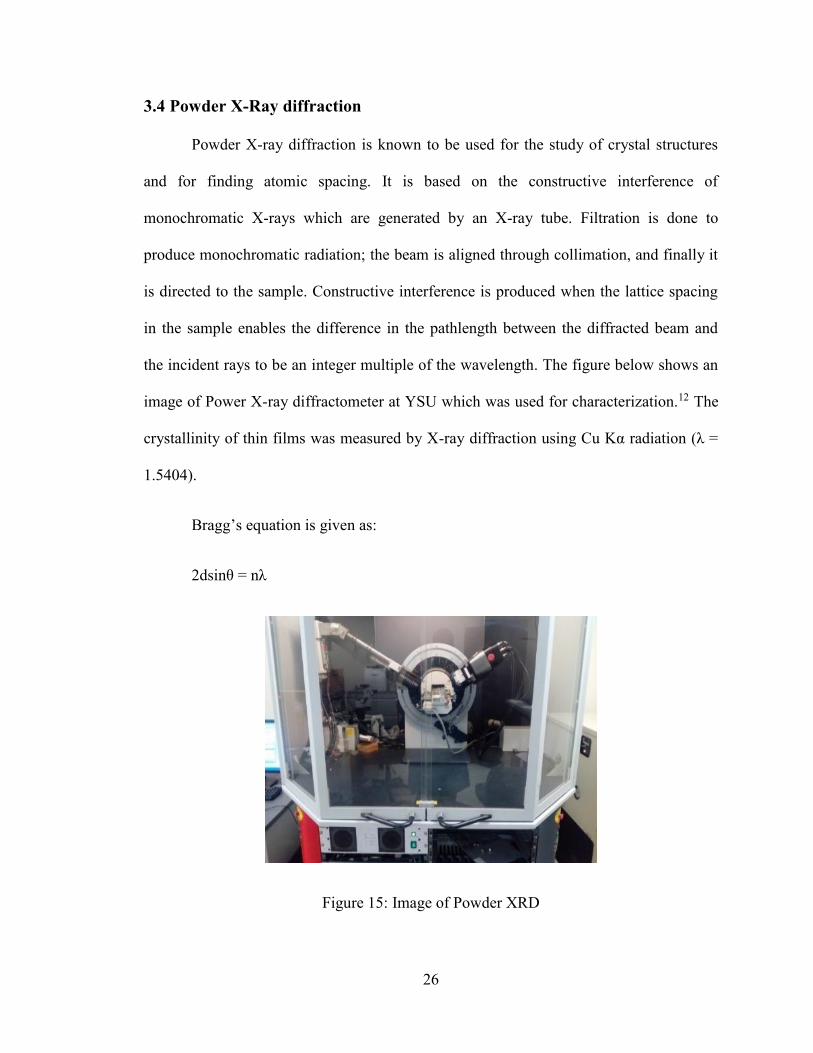
3.4 Powder X-Ray diffraction
Powder X-ray diffraction is known to be used for the study of crystal structures
and for finding atomic spacing. It is based on the constructive interference of
monochromatic X-rays which are generated by an X-ray tube. Filtration is done to
produce monochromatic radiation; the beam is aligned through collimation, and finally it
is directed to the sample. Constructive interference is produced when the lattice spacing
in the sample enables the difference in the pathlength between the diffracted beam and
the incident rays to be an integer multiple of the wavelength. The figure below shows an
image of Power X-ray diffractometer at YSU which was used for characterization.12 The
crystallinity of thin films was measured by X-ray diffraction using Cu Kα radiation (λ =
1.5404).
Bragg’s equation is given as:
2dsinθ = nλ
Figure 15: Image of Powder XRD
27
3.5 Scanning electron microscopy (SEM)
A scanning electron microscope is a type of electron microscope that can produce
high resolution images of a sample by scanning it with a focused beam of electrons.
SEM–EDX technique was used to provide detailed imaging information about the
morphology and surface texture of individual particles, as well as elemental composition
of samples. In our study, the sample was cut into approximately 3 mm × 4 mm pieces and
mounted in the SEM-EDS chamber. The electrons interact with atoms in the sample,
producing secondary electron signals that can be detected and that contain information
about the sample's surface topography and composition. The electron beam is generally
scanned in a raster scan pattern, and the beam's position is combined with the detected
signal to produce an image. An SEM with sufficient beam voltage and sample enables the
difference in pathlength between the diffracted beam conductivity can achieve resolution
better than 1 nm.
Working principle of SEM
SEM mainly uses a beam of electrons which are ejected or emitted terminally from a
tungsten or lanthanum hexaboride (Lab6) cathode and accelerated towards the anode.
Tungsten is used simply because it has high melting point and a low vapor pressure,
hence allowing it to be heated for electron emission. The electron beam has an energy
that ranges from a few hundred eV to 100 KeV and is focused by a condenser lens into a
beam with a very fine focal spot. The beam goes through scanning coils in the objective
lens, which deflects the beam horizontally and vertically so that it scans in a raster
fashion over a rectangular area of the sample surface. As the electron beam interacts with
the sample, the electrons lose energy by repeated scattering and absorption within a
28
teardrop-shaped volume of the specimen known as the interaction volume, which extends
from less than 100 nm to around 5 micrometers into the surface. The size of the
interaction volume depends on the electrons’ landing energy and the atomic number of
the sample. This results in the emission of electrons and electromagnetic radiation, which
lead to detection of the image.13
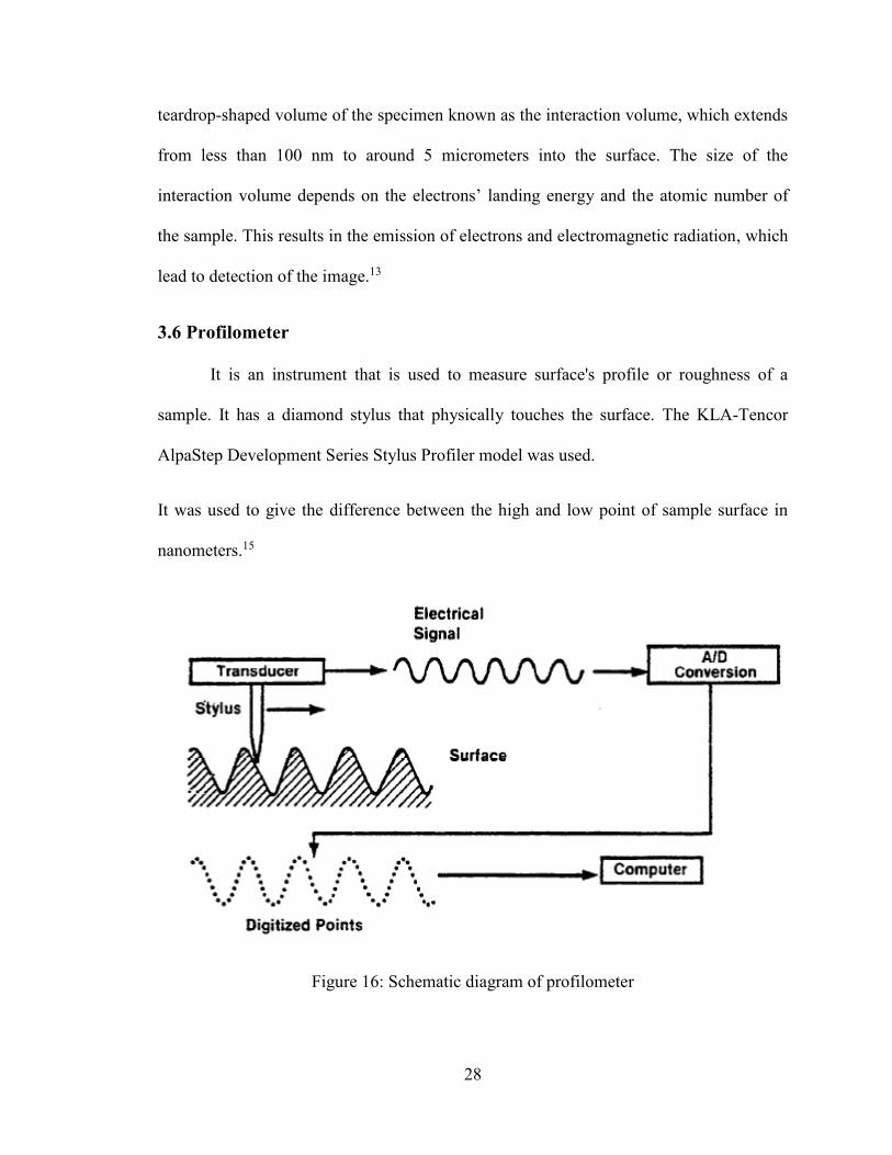
3.6 Profilometer
It is an instrument that is used to measure surface's profile or roughness of a
sample. It has a diamond stylus that physically touches the surface. The KLA-Tencor
AlpaStep Development Series Stylus Profiler model was used.
It was used to give the difference between the high and low point of sample surface in
nanometers.15
Figure 16: Schematic diagram of profilometer

29
Working principle of profilometer
The KLA-Tencor is computerized and has high sensitivity surface profiler that measures
step height, roughness and waviness in a variety of applications on the surfaces. It
measures precision heights from under 10 angstroms to as large as 1.2 millimeters. It
does this by incorporating a new optical deflection height measurement mechanism and
magneto static force control system that results in a low force and low inertia stylus
assembly. The scan parameters such as speed, length, sampling rate and force to applied
are set. By using high force it gives high resolution of the sample .The scan gives a graph
of the data. Both height and width can be measured moving R and M scale parameters to
level the graph of the data.
3.7 Photoluminescence experiment
Photoluminescence (PL) is an important physical phenomenon used to
characterize semiconductors which depicts the electronic structure of the materials while
possibly revealing other important material features. In brief, PL occurs when a
photovoltaic cell absorbs light of energy higher than the bandgap. This results in the
creation of electrons and holes in excess of their thermal equilibrium concentrations.
After thermal relaxation, the excess electrons and holes recombine with a consequence of
photon emission (radiative recombination) with lower energy than the excitation photons.
The recombination is accomplished either directly (such as band-to-band recombination –
electrons in the conduction band recombining with holes in the valence band) or more
frequently, involving one or more intermediate states such as bound excitons and
impurities or defects with an energy level inside the forbidden gap.
30
Chapter 4
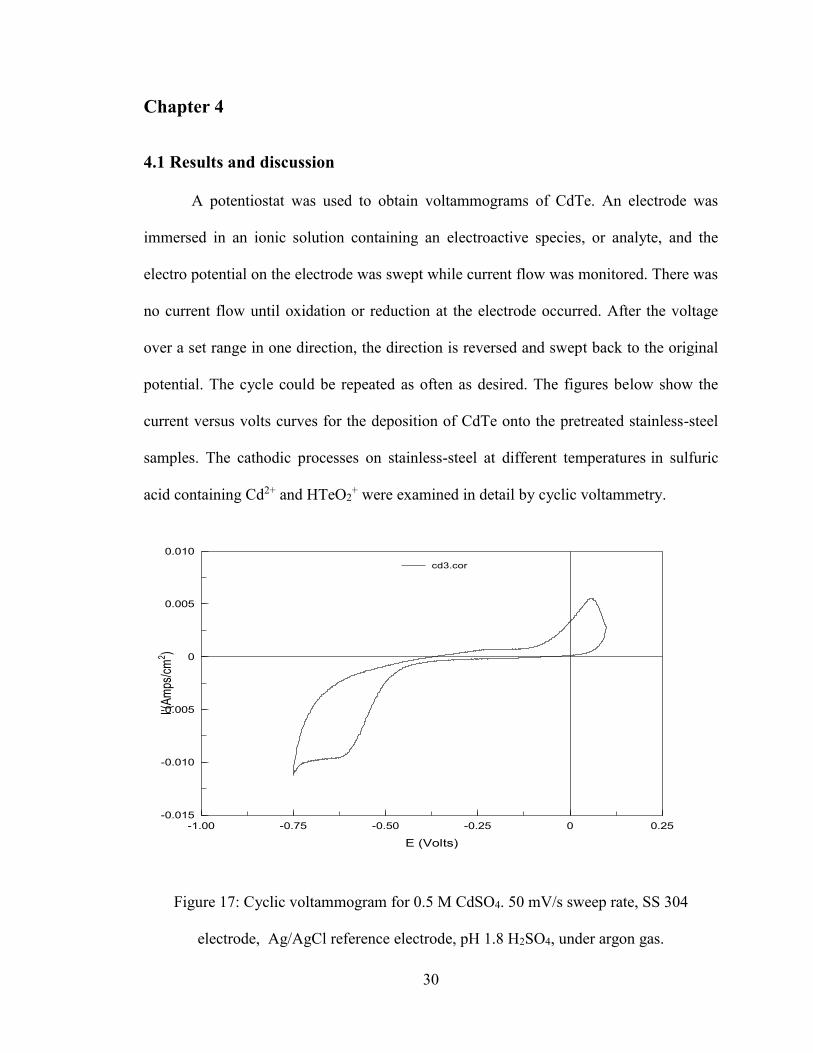
4.1 Results and discussion
A potentiostat was used to obtain voltammograms of CdTe. An electrode was
immersed in an ionic solution containing an electroactive species, or analyte, and the
electro potential on the electrode was swept while current flow was monitored. There was
no current flow until oxidation or reduction at the electrode occurred. After the voltage
over a set range in one direction, the direction is reversed and swept back to the original
potential. The cycle could be repeated as often as desired. The figures below show the
current versus volts curves for the deposition of CdTe onto the pretreated stainless-steel
samples. The cathodic processes on stainless-steel at different temperatures in sulfuric
acid containing Cd2+ and HTeO2+ were examined in detail by cyclic voltammetry.
Figure 17: Cyclic voltammogram for 0.5 M CdSO4. 50 mV/s sweep rate, SS 304
electrode, Ag/AgCl reference electrode, pH 1.8 H2SO4, under argon gas.
-1.00 -0.75 -0.50 -0.25 0 0.25-0.015
-0.010
-0.005
0
0.005
0.010
E (Volts)
I (Am
ps/cm
2 )
cd3.cor
31
For initial characterization of Cd electrodeposition was performed to identify Faradaic
activity by applying a voltage of -0.75 V. the ionic liquid was purged with argon and the
voltammetric experiments were performed using a 273 PAR potentiostat driven by
CorrWare. With a negative voltage limit equal to -0.5 V, the onset of a cathodic was
observed (Figure 17). Thus, it was discovered that the supposed cathodic solvent limit
probed in the figure above was the onset of a voltammetric wave with peak at -0.5 V and
not more than -0.75 V.
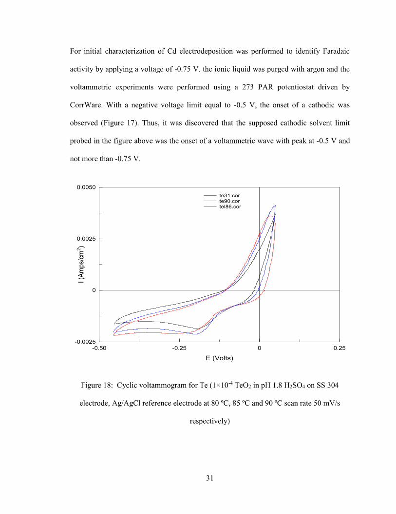
Figure 18: Cyclic voltammogram for Te (1×10⁻⁴ TeO2 in pH 1.8 H2SO4 on SS 304
electrode, Ag/AgCl reference electrode at 80 ºC, 85 ºC and 90 ºC scan rate 50 mV/s
respectively)
-0.50 -0.25 0 0.25-0.0025
0
0.0025
0.0050
E (Volts)
I (Am
ps/c
m2 )
te31.corte90.cortel86.cor
32
Cyclic voltammetry was performed to show temperature effect on the
electrodeposition of tellurium. With a negative voltage limit equal to -0.45 V, the onset of
a cathodic reduction as observed above (Figure 17) started at voltage of about -0.2 V.
Thus, it was discovered that the supposed cathodic solvent limit probed in the figure
above was the onset of a voltammetric wave where we expect tellurium reduction.
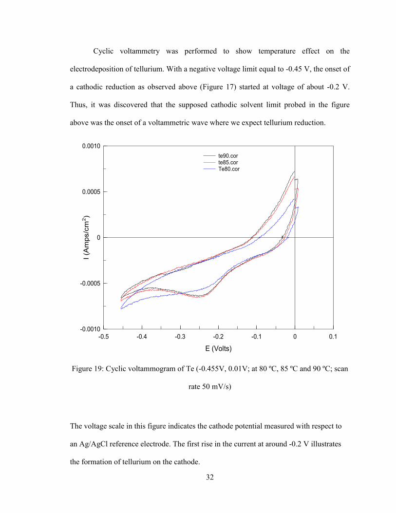
Figure 19: Cyclic voltammogram of Te (-0.455V, 0.01V; at 80 ºC, 85 ºC and 90 ºC; scan
rate 50 mV/s)
The voltage scale in this figure indicates the cathode potential measured with respect to
an Ag/AgCl reference electrode. The first rise in the current at around -0.2 V illustrates
the formation of tellurium on the cathode.
-0.5 -0.4 -0.3 -0.2 -0.1 0 0.1-0.0010
-0.0005
0
0.0005
0.0010
E (Volts)
I (A
mps
/cm
2 )
te90.corte85.corTe80.cor

33
Figure 20: Temperature dependence cyclic voltammogram of CdTe deposition on bare
SS 304, 0.5 M CdSO4, 1×10⁻⁴ TeO2 in pH 1.8 H2SO4 (-0.455V, 0.01V; at 80 ºC, 85 ºC
and 90 ºC; scan rate 50 mV/s)
In order to determine the electrodeposition mechanism and the codeposition
potential for CdTe precursor, cyclic voltammetry measurements were performed on bare
stainless steel substrate. It was observed in the Figure 20 above that by sweeping
voltammogram to the cathodic limit on a bare stainless steel substrate started a wave that
showed up at -0.25 V.
This indicated that CdTe deposition took place for cathode potentials between -
0.2 V and -0.5 V. The temperature was varied as seen in the three cycles above. It was
-0.5 -0.4 -0.3 -0.2 -0.1 0 0.1-0.0015
-0.0010
-0.0005
0
0.0005
E (Volts)
I (A
mps
/cm
2 )
cdte90.corcdte85.corcdte80.cor

34
observed that increase in temperature resulted in increase of currents too. From the waves
observed it was noted that electrodeposition of CdTe on a bare stainless steel substrate
does not yield a good result of reduction. A light thin film of grey deposition was
observed on the substrate.
Figure 21: Cyclic voltammogram of CdTe deposition onto a Te/stainless steel 304
substrate 0.5 M CdSO4, 1×10⁻⁴ M TeO2, pH 1.8 H2SO4, Ar atmosphere’ Ag/AgCl
reference electrode at (80 ºC, 85 ºC and 90 ºC; scan rate 50 mV/s ).
It was observed in the Figure 21 above that the onset of cathodic reduction is
slightly lower than the previous one. Stirring and heating was done as well. The
difference seen is a result of depositing of CdTe on a Te/SS 304 substrate. This
voltammogram gave a reversible wave. The temperature too was varied as previous and
35
still reversible waves were obtained. It was noted that cadmium undergoes underpotential
deposition (UPD) as shown in Figure 21 above. UPD is a surface-limited phenomenon
that results in a limited deposition of atoms at a potential positive of its normal Eº. CdTe
was codeposited, in that both elements were deposited at a constant potential from the
same solution. It is noted that cadmium has a strong preference to be to deposited onto a
tellurium layer as opposed to a bare stainless steel substrate. For this case it is observed
that cadmium UPD peak shifted towards a more positive potential as compared to that of
a bare substrate. Hence in conclusion it shows that the interaction of CdTe/Te/SS 304 and
CdTe/SS 304 is not the same.
Figure 22: Cyclic voltammogram for sweep rate dependence of the photoelectrolysis on
SS 304 in darkness, Ag/AgCl ref. electrode
-0.5 -0.4 -0.3 -0.2 -0.1 0 0.1-0.0005
0
0.0005
0.0010
E (Volts)
I (A
mps
/cm
2 )
[email protected]@[email protected]@dark200.cor
36
Figures 22 pH 1.8 H2SO4 was used as control. A flat baseline of about 0.25 MmAa for
electrodeposition of other substances
Figure 23: Sweep rate dependence for cyclic voltammogram of CdTe film on Te/SS 304
in the light using xenon lamp.
Sweeping the potential at different rates resulted in an increase of current as the
sweep rates were increased. Each curve in the figure above has the same form and it was
observed that the total current increases with increasing sweep rate. It was noted that the
linear sweep voltammogram took longer to record as the sweep rate was decreased.

37
4.1 Electrodeposition trials
The oxygen evolution reaction, which is oxidation of water, is one of the
important reactions that occur at the anode. It is coupled with other important reactions
such as hydrogen evolution in water splitting. The factors such as mechanism of electrode
reaction, kinetics, thermodynamics, effective surface area, conductivity and chemical and
mechanical stability were put into consideration for an overall performance.
It was first necessary to deposit a thin underlayer of Te. The potentiostat was set
to sweep negative from 0.001 V at 50 mV/s and hold at -0.45 V for 480 s for Te and 600
s for CdTe. Stirring and heating was performed while argon gas was bubbled in the cell
for purging. The current verses time profiles from Te deposition are shown below. We
were able to observe dark grey deposition on the substrate.
Figure 24: Electrodeposition of Te at 80º C, for 480 s
0 100 200 300 400 500-0.0020
-0.0015
-0.0010
-0.0005
0
Time (Sec)
I (A
mps
/cm
2 )
TeO2oct17.cor
38
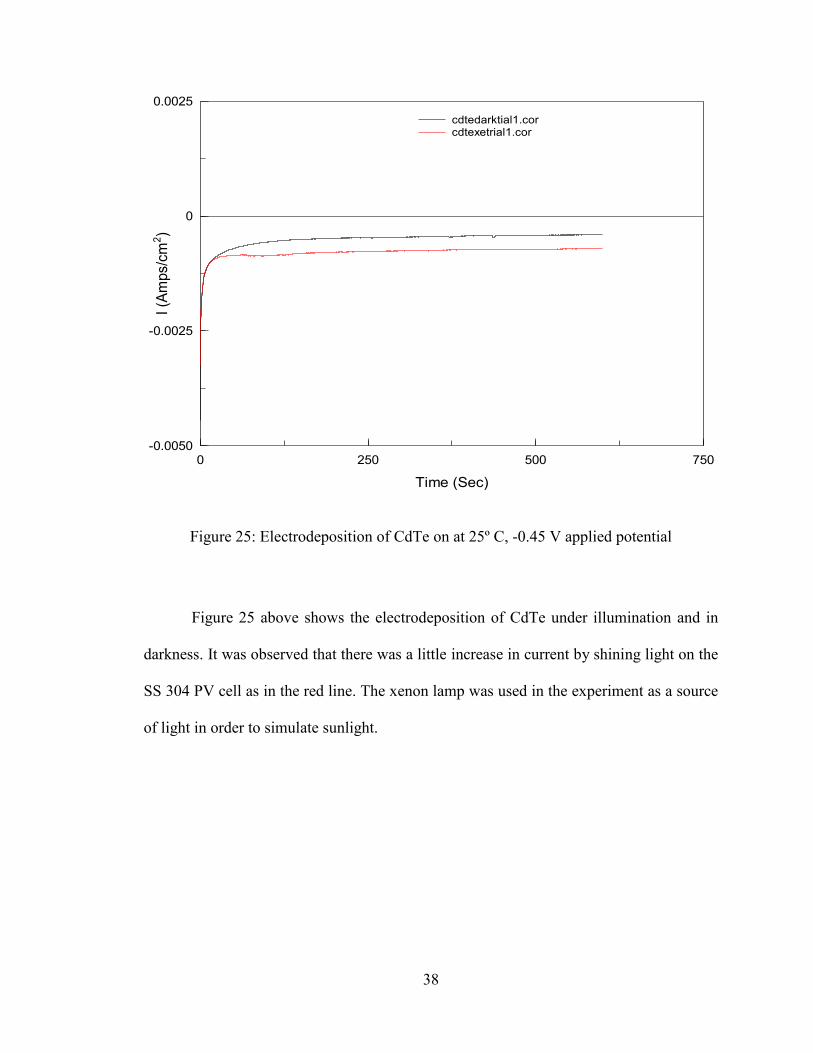
Figure 25: Electrodeposition of CdTe on at 25º C, -0.45 V applied potential
Figure 25 above shows the electrodeposition of CdTe under illumination and in
darkness. It was observed that there was a little increase in current by shining light on the
SS 304 PV cell as in the red line. The xenon lamp was used in the experiment as a source
of light in order to simulate sunlight.
0 250 500 750-0.0050
-0.0025
0
0.0025
Time (Sec)
I (Am
ps/c
m2 )
cdtedarktial1.corcdtexetrial1.cor

39
Figure 26: Electrodeposition of CdTe at 80º C, -0.45 V
In Figure 26 above, to allow for longer cathodic electrolysis times, a sweep-and-hold was
performed. The working electrode was swept from 0 to -0.45 V at 50 mV/s. At that point,
argon purging was started. The experiment was stopped at 480 s or 8 minutes in tellurium
deposition, and 600 s in other trials. The chronoamperometric data is as shown in the
Figure 26 above. For longer cathodic electrolysis times in order to deposit CdTe, time
was extended to 7200 s.
0 250 500 750-0.004
-0.003
-0.002
-0.001
0
Time (Sec)
I (A
mps
/cm
2 )
cdtexetrial1.cor
40
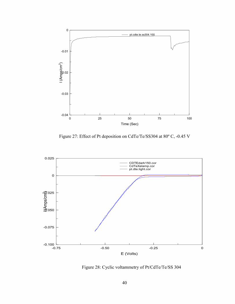
Figure 27: Effect of Pt deposition on CdTe/Te/SS304 at 80º C, -0.45 V
Figure 28: Cyclic voltammetry of Pt/CdTe/Te/SS 304
0 25 50 75 100-0.04
-0.03
-0.02
-0.01
0
Time (Sec)
I (Am
ps/c
m2 )
pt.cdte.te.ss304.100
-0.75 -0.50 -0.25 0-0.100
-0.075
-0.050
-0.025
0
0.025
E (Volts)
I (Am
ps/cm
2 )
CDTEdark150.corCdTeXelamp.corpt.dte.light.cor
41
The effect of platinum on electrodeposited CdTe was tested with just some few
seconds remaining before electrolysis was stopped as seen in Figure 27 above. It was
observed that there was an increase of bubbles of hydrogen gas. This was done by
sprinkling little amount of chloroplatinic acid into the electrolyte. This is so because
platinization of the CdTe photovoltaic cell makes its kinetics of H2 gas evolution
increase. It was noted that there was an increase in current due to platinum activation, as
seen in the hydrogen peak displayed in Figure 28. Performing photoelectrochemistry both
in the dark and light did not show any change in current as seen in Figure 28 above. It
was concluded that platinization activated the surface of the electrodes.
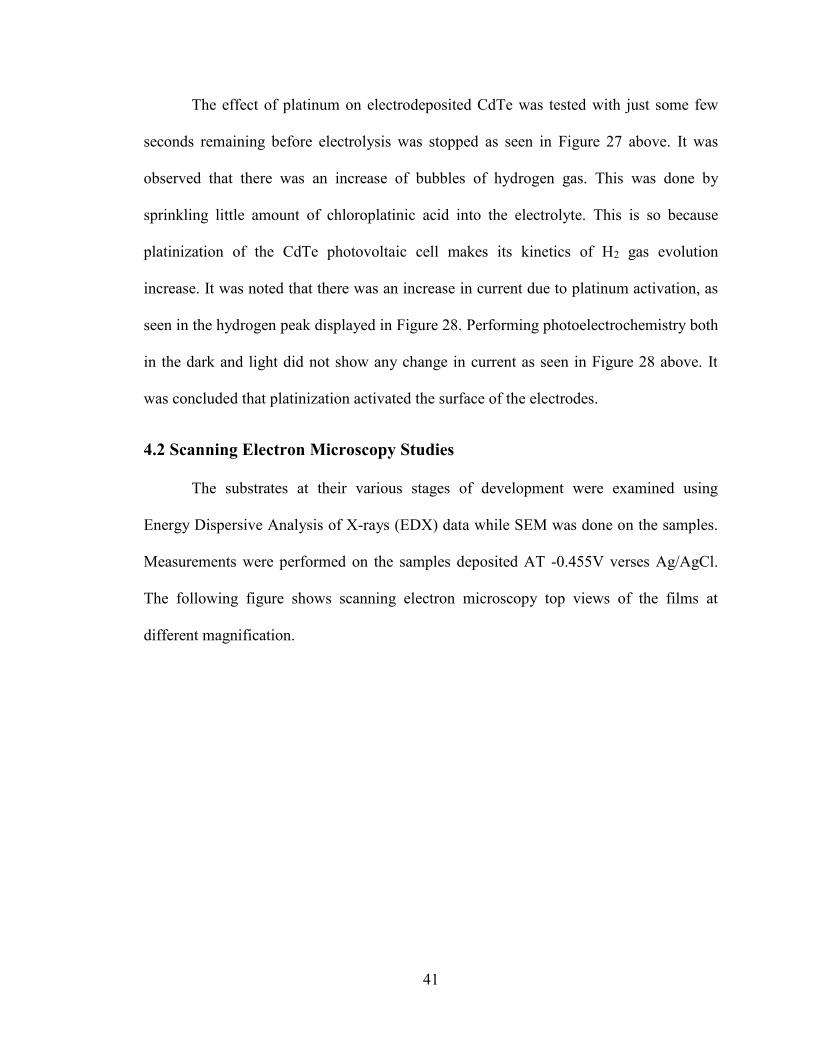
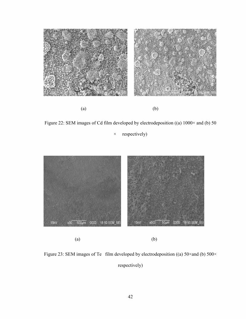
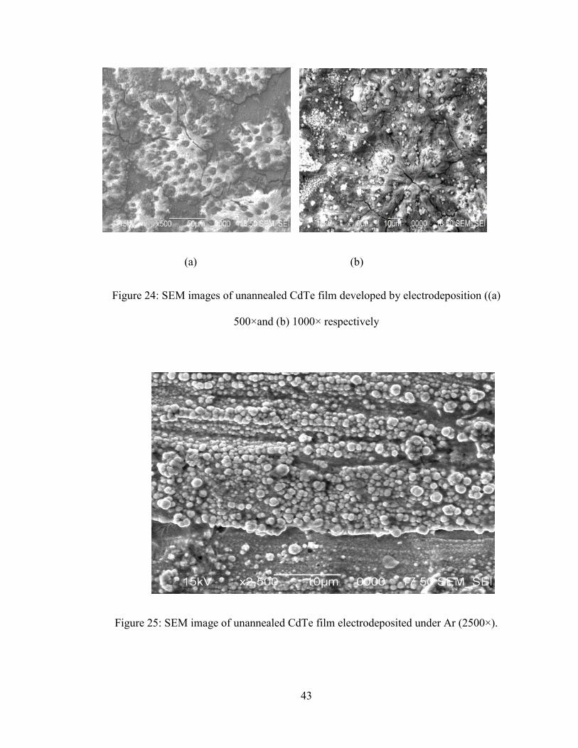
4.2 Scanning Electron Microscopy Studies
The substrates at their various stages of development were examined using
Energy Dispersive Analysis of X-rays (EDX) data while SEM was done on the samples.
Measurements were performed on the samples deposited AT -0.455V verses Ag/AgCl.
The following figure shows scanning electron microscopy top views of the films at
different magnification.
42
(a) (b)
Figure 22: SEM images of Cd film developed by electrodeposition ((a) 1000× and (b) 50
× respectively)
(a) (b)
Figure 23: SEM images of Te film developed by electrodeposition ((a) 50×and (b) 500×
respectively)
43
(a) (b)
Figure 24: SEM images of unannealed CdTe film developed by electrodeposition ((a)
500×and (b) 1000× respectively
Figure 25: SEM image of unannealed CdTe film electrodeposited under Ar (2500×).
44
Figure 26: SEM images of annealed CdTe film at 350oC (3500×, 3000× and 1400×
respectively)
SEM images at different magnifications are shown in the figures above from various spot
areas of the sample to show the film quality in different regions. As seen above some of
the SEM images show cracks on the surface. The cracks can arise from incomplete
coalescence of the CdTe grains during deposition or be due to defects in the underlying
surface or may have been developed during annealing process. The films were allowed to
cool to room temperature to avoid building up of stress in the films.
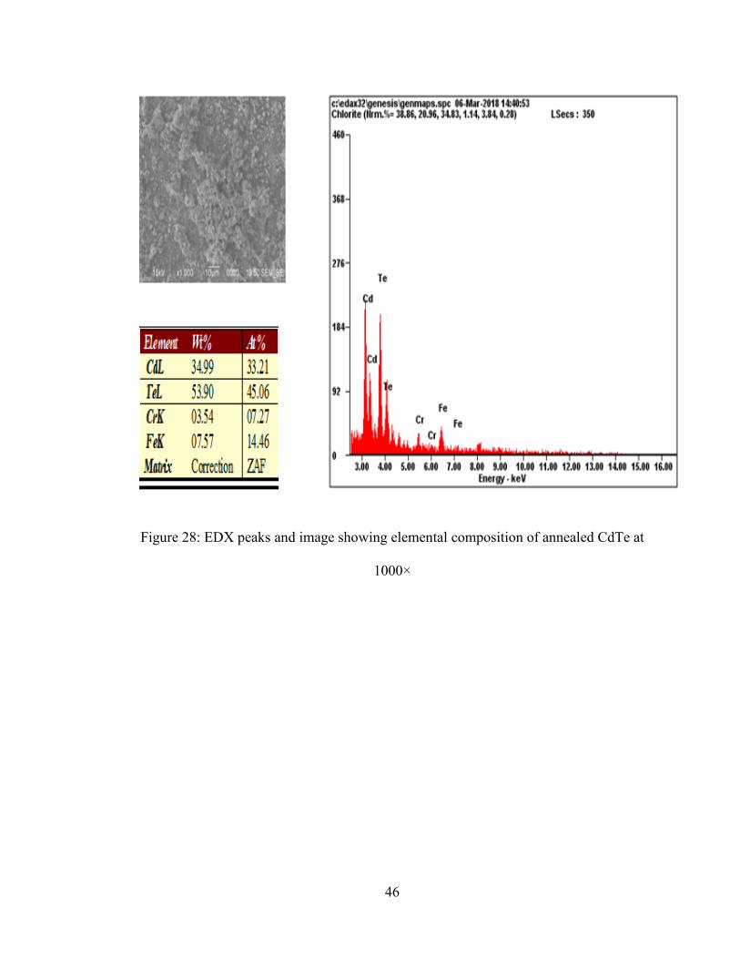
Below is the EDX data showing elemental composition of the sample. The spectra
of unannealed sample shows the present of Cd and Te while in the annealed sample it is
observed that there is addition of chromium and Iron.16 These additional elements found
45
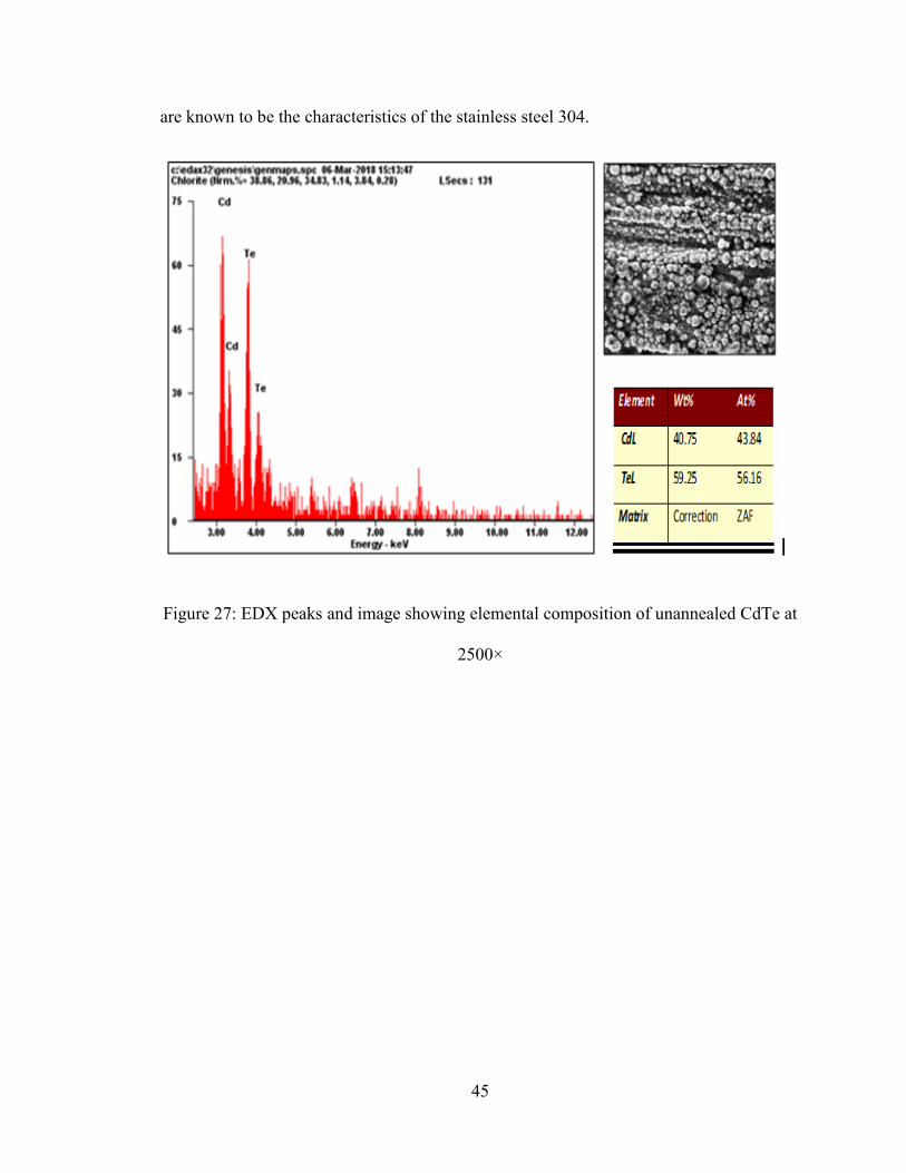
are known to be the characteristics of the stainless steel 304.
Figure 27: EDX peaks and image showing elemental composition of unannealed CdTe at
2500×
46
Figure 28: EDX peaks and image showing elemental composition of annealed CdTe at
1000×
47
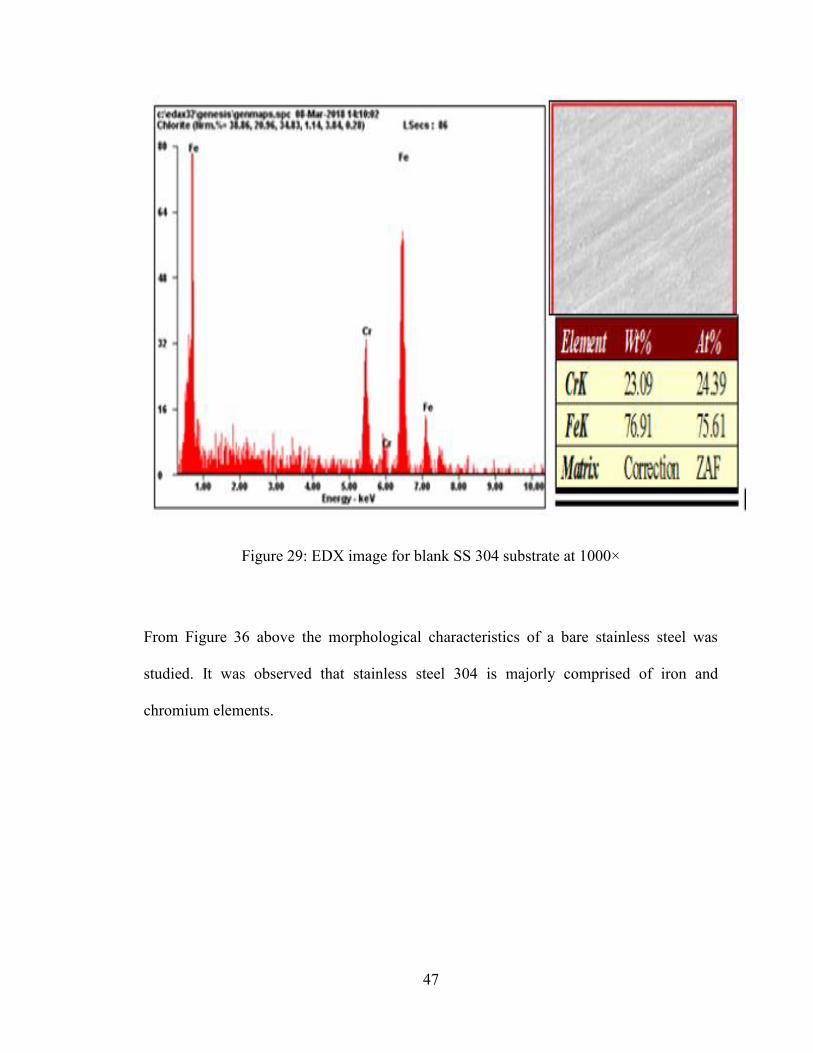
Figure 29: EDX image for blank SS 304 substrate at 1000×
From Figure 36 above the morphological characteristics of a bare stainless steel was
studied. It was observed that stainless steel 304 is majorly comprised of iron and
chromium elements.
48
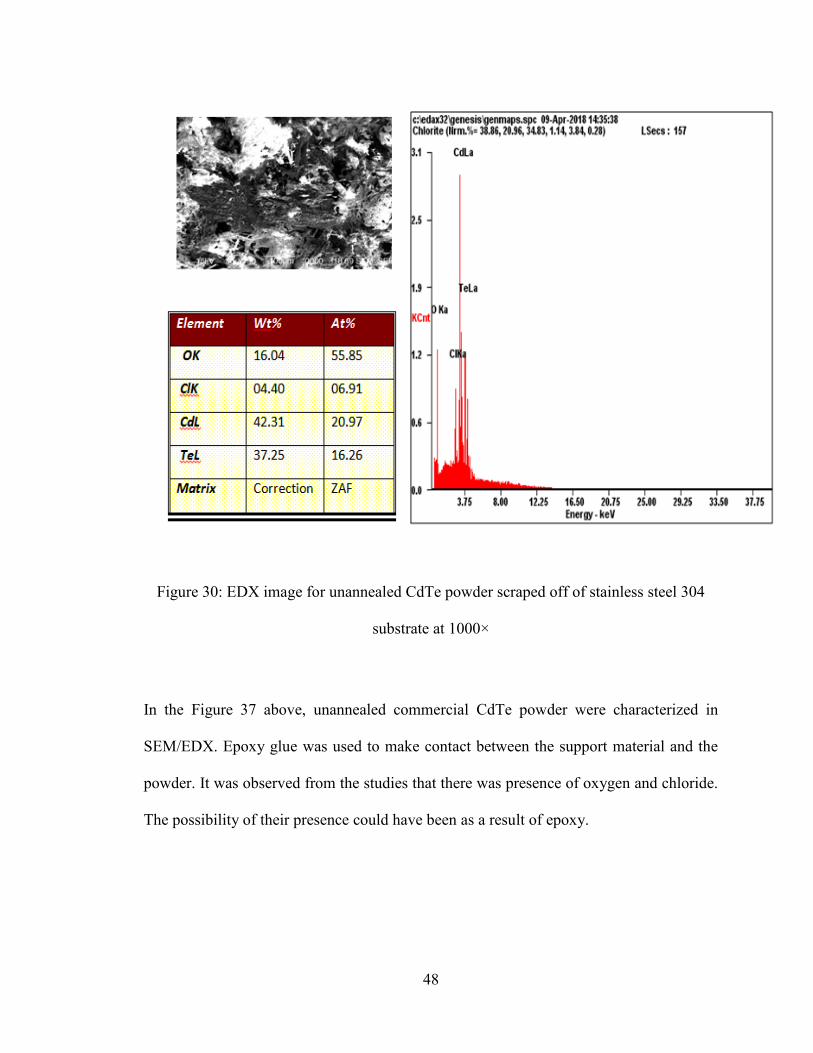
Figure 30: EDX image for unannealed CdTe powder scraped off of stainless steel 304
substrate at 1000×
In the Figure 37 above, unannealed commercial CdTe powder were characterized in
SEM/EDX. Epoxy glue was used to make contact between the support material and the
powder. It was observed from the studies that there was presence of oxygen and chloride.
The possibility of their presence could have been as a result of epoxy.
49
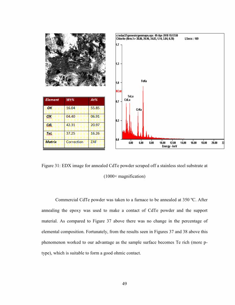
Figure 31: EDX image for annealed CdTe powder scraped off a stainless steel substrate at
(1000× magnification)
Commercial CdTe powder was taken to a furnace to be annealed at 350 ºC. After
annealing the epoxy was used to make a contact of CdTe powder and the support
material. As compared to Figure 37 above there was no change in the percentage of
elemental composition. Fortunately, from the results seen in Figures 37 and 38 above this
phenomenon worked to our advantage as the sample surface becomes Te rich (more p-
type), which is suitable to form a good ohmic contact.

50
Figure 32: PXRD image for CdTe deposited on SS 304
51
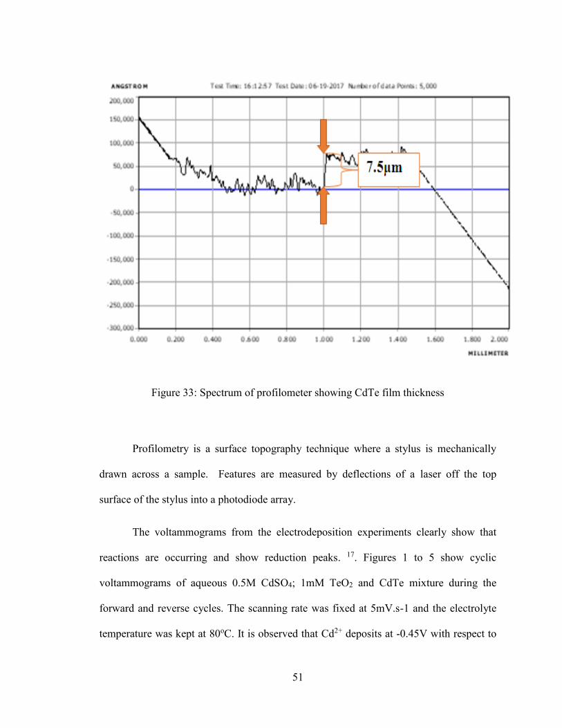
Figure 33: Spectrum of profilometer showing CdTe film thickness
Profilometry is a surface topography technique where a stylus is mechanically
drawn across a sample. Features are measured by deflections of a laser off the top
surface of the stylus into a photodiode array.
The voltammograms from the electrodeposition experiments clearly show that
reactions are occurring and show reduction peaks. 17. Figures 1 to 5 show cyclic
voltammograms of aqueous 0.5M CdSO4; 1mM TeO2 and CdTe mixture during the
forward and reverse cycles. The scanning rate was fixed at 5mV.s-1 and the electrolyte
temperature was kept at 80oC. It is observed that Cd2+ deposits at -0.45V with respect to
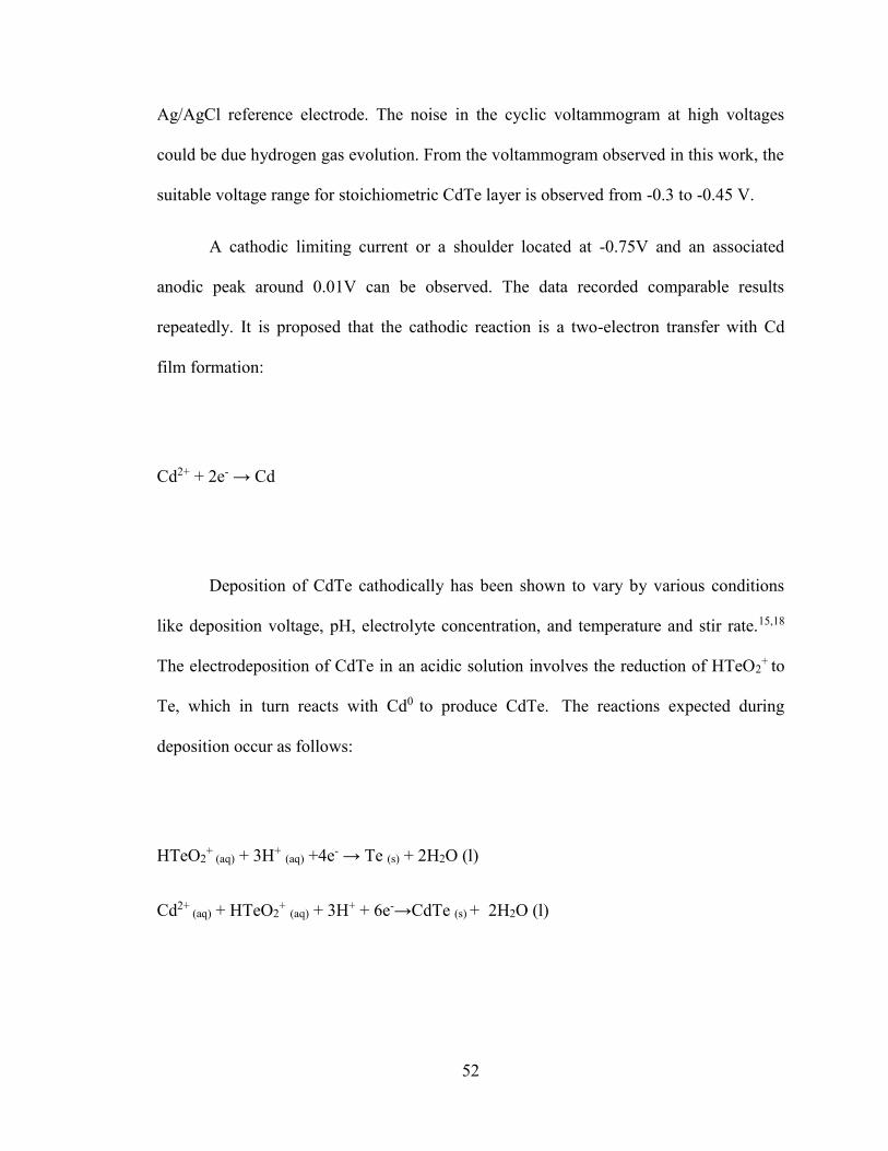
52
Ag/AgCl reference electrode. The noise in the cyclic voltammogram at high voltages
could be due hydrogen gas evolution. From the voltammogram observed in this work, the
suitable voltage range for stoichiometric CdTe layer is observed from -0.3 to -0.45 V.
A cathodic limiting current or a shoulder located at -0.75V and an associated
anodic peak around 0.01V can be observed. The data recorded comparable results
repeatedly. It is proposed that the cathodic reaction is a two-electron transfer with Cd
film formation:
Cd2+ + 2e- → Cd
Deposition of CdTe cathodically has been shown to vary by various conditions
like deposition voltage, pH, electrolyte concentration, and temperature and stir rate.15,18
The electrodeposition of CdTe in an acidic solution involves the reduction of HTeO2+ to
Te, which in turn reacts with Cd0 to produce CdTe. The reactions expected during
deposition occur as follows:
HTeO2+
(aq) + 3H+ (aq) +4e- → Te (s) + 2H2O (l)
Cd2+ (aq) + HTeO2
+ (aq) + 3H+ + 6e-→CdTe (s) + 2H2O (l)

53
From the SEM images it was observed that annealing temperature of 350 ͦC which
enhanced nucleation led to formation of large grains18. By treating with CdCl2 the CdTe
layers grown in this work showed a compact grain growth without gaps. This suggests
that CdCl2 treated CdTe produced from chloride precursor has a better quality as seen in
the SEM images19,20.
The thickness of the electrodeposited CdTe layer on the SS 304 was calculated
experimentally by using a profilometer. The highest reading that was seen in the
profilometry was 75000 Armstrong as shown in the Figure 40 above. From the
measurements made an approximate of 7.5 micrometers of film thickness was obtained.
4.3 Powder X-Ray Diffraction (PXRD)
The X-ray diffraction studies were carried out on as-deposited CdTe layers and
typical results are shown in Figure 35 below. In this study, CdTe thin films were
electrodeposited at a voltage of 450 mV vs Ag/AgCl. According to Figure, the graph
shows the presence of the noticeable peak of CdTe at 2θ = 24.15° corresponding to the
(111) cubic phase. However, the pattern displays six diffraction peaks values at 47.2,
63.1, 72 and 77.5, which correspond to the diffraction lines produced by the (311), (331),
(422) and (511) crystalline planes of cubic CdTe, respectively. The large peaks shown
correspond to iron.
CdTe samples were annealed under an ambience of argon. For CdCl2 presoaking
is well known that its treatment usually improves the crystallinity of CdTe up to a certain
temperature. 21

54
4.4 Film thickness/profilometry
The film thickness was calculated as per the formula;
For Te, the deposition current is at most 1 mA. Therefore,
μm=(i.t.fw)/(nFQA)
=[current(C/s)(time(s)(FW(g/mol)]/ [F(coul/eq)(4 eq/mol)(density, g/cm3)(A,cm2)]
=[(1E-3)(8 min)(60 s/min)(127.6 g/mol)(1E-4 μm/cm)] ÷
[(96485C/eq)(4 eq/mol)(6.25g/cm3)(2cm2)]
=0.127 μm; or 127 nm.
Calculating for film thickness CdTe resulted in about 8 μm as shown in calculations
below.
=[current(C/s)(time(s)(FW(g/mol)]/ [F(coul/eq)(eq/mol)(density, g/cm3)(A,cm2)]
=[(1E-3)(120 mins)(60 s/min)(240 g/mol)(1E-4μm/cm)] ÷
[(96485 C/eq)(2 eq/mol)(5.85 g/cm) (2cm2)]
=7.6 μm.

55
This is so impressive as far as thin film thickness is necessary in making CdTe
photovoltaic cell. The results from the profilometer as seen in Figure 40 above shows a
film thickness of approximately 0.75 μm
In conclusion, we have obtained information from XRD and SEM
characterization techniques indicating the growth of a new film on the substrate and the
formation of CdTe.
Chapter 5
5.1 Conclusion and future work
In this work it was demonstrated that the electrodeposition of CdTe on SS-304 is
feasible. Thin films of CdTe were grown by applying a potential of -0.45 V verses
Ag/AgCl for 120 min to give a film thickness of approximately 7-10 µm. Structural and
optical properties of these films were investigated by using various characterization
techniques. Powder XRD analysis showed that CdTe films are cubic polycrystalline and
has a preferred orientation in (111) direction. Furthermore, annealing improves
crystallinity in the CdTe films. Energy Dispersive X-ray Spectroscopy (EDS) was used to
acquire detailed imaging information about the morphology and surface texture, as well
as elemental composition of the film.
Thin films of CdTe have been successfully grown through an electrodeposition
method as seen from the SEM images. The visual appearances, surface morphology,

56
elemental and optical properties of CdTe layers were grown on the stainless steel 304
substrates are shown.
It was noted that platinization of the CdTe photovoltaic cell made the kinetics of
H2 gas evolution to increase by nearly two orders of magnitude. The voltammetric results
presented here and other relevant information from the literature lead to the following
conclusions. It is noted that cadmium has a strong preference to be deposited onto a
tellurium layer as opposed to a bare stainless steel substrate. By performing
electrodeposition it was observed that cadmium UPD peak shifted towards a more
negative potential in comparison to that of a bare substrate. Use X-ray photoelectron
spectroscopy to measure elemental composition of Cd and Te. Increasing substrate
temperature can passivate grain boundaries and improve grain integrity effectively, along
with decreased radiative recombination.

57
References
1. Xavier Mathew J. Pantoja Enriquez, Alessandro Romeo and Ayodhya N.
Tiwari. CdTe/CdS Solar cells on flexible substrates. Solar Energy 77 (2004)
831–838.
2. A. Morales-Acevedo / Solar Energy 80 (2006) 675–681
3. Kroger, F.A., Rod, R.L, 1979. Photovoltaic power generating means and
methods. UK patent 1532616, February (1979); Kroger, F.A., Rod, R.L.,
Panicker M.P, R., 1983, US patent 4400244, August (1983).
4. Atef Y. Shenouda, El Sayed M. El Sayed. Electrodeposition, characterization
and photo electrochemical properties of CdSe and CdTe. July 2014.
5. Adolf Goetzberger ChristopherHebling Hans-WernerSchockPhotovoltaic
materials, history, status and outlook. 1 January 2003, Pages 1-46.
6. https://en.wikipedia.org/wiki/Cadmium_telluride_photovoltaics, March 2017.
7. Abdul-Manaf, N.; Salim, H.; Madugu, M.; Olusola, O.; Dharmadasa, I. Electro-
plating and characterisation of CdTe thin films using CdCl2 as the cadmium
source. Energies 2015, 8, 10883–10903.
8. Allen J. Bard and Marye Anne Fox. Artificial Photosynthesis: Solar Splitting of
Water to Hydrogen and Oxygen. Acc. Chem. Res. 1995,28, 141-145 141.
9. Salim, H.I.; Patel, V.; Abbas, A.; Walls, J.M.; Dharmadasa, I.M.
Electrodeposition of CdTe thin films using nitrate precursor for applications in
solar cells. J. Mater. Sci. Mater. Electron. 2015, 26, 3119–3128.
10. Characterization and annealing of CdTe thin film prepared by vapor transport
deposition Ren. A, Vol. 12, No. 11, November 2015, p. 555 – 567

58
11. Nor A. Abdul-Manaf et al, ‘Electroplating and characterization of CdTe thin
films using CdCl2 as the cadmium source. September 2015.
12. https://serc.carleton.edu/research_education/geochemsheets/techniques/XRD.ht
ml.
13. http://www.bionity.com/en/encyclopedia/Scanning_electron_microscope.html.
14. https://en.wikipedia.org/wiki/X-ray_photoelectron_spectroscopy.
15. http://www.nyarkuscanopies.com/site/r6s6d.php?tr=how-to-measure-surface-
roughness-using-profilometer.
16. Imyhamy M. Dharmadasa et al, ‘Electroplating of CdTe Thin Films from
Cadmium Sulphate Precursor and Comparison of Layers Grown by 3-Electrode
and 2-Electrode Systems.’ Coatings 2017, 7(2), 17.
17. A. J. Bard and L. R. Faulkner, Electrochemical Methods: Fundamentals and
Applications, 2nd ed. Wiley, 2000.
18. Stephen L. N. H. R; Howard D. M; Clovis A. L. Development of a hydrogen
evolving photocatalytic membrane. (2012).
19. Nor A; Hussein I. S; Mohammad L. M; Olajide I. O; Imyhamy M. D. Electro-
Plating and Characterisation of CdTe Thin Films Using CdCl2 as the Cadmium
Source. 2015, 8, 10883-10903.
20. Atapattu H. Y. R; Dharmadasa I. M. Effect of stirring rate of electrolyte on
properties of electrodeposited CdS layers, Journal of Materials Science:
Materials in Electronics (2016).

59
21. Imyhamy M. Dharmadasa, ‘Effects of CdCl2 treatment on deep levels in CdTe
and their implications on thin film solar cells: A comprehensive
photoluminescence study. April 2015.
22. J Li,Y F Zheng, J B Xu and K Dai. Te-doped cadmium telluride films fabricated
by close spaced sublimation.
23. A. G. Voloshchuk and N. I. Tsipishchuk. Equilibrium Potential–pH Diagram of
the CdTe–H2O System. Vol. 38, No. 11, 2002, pp 1320–1323.
24. Xinjian Yi Li and Liping Cai. Study on surface oxidative characterization of
LPE HgCdTe epilayer by Xray photoelectron spectroscopy. July 1999.
25. Alan L. Fahrenbruch. Ohmic contacts and doping of CdTe. July 3 1986
26. Irvine, S.J.C. Barrioz, V., Stafford, A., Durose, K.,Thin Solid Films 480–481
(2005) 76-81.
Related Documents


