Electrically-tunable hole g-factor of an optically-active quantum dot for fast spin rotations Jonathan H. Prechtel, 1, * Franziska Maier, 1 Julien Houel, 2 Andreas V. Kuhlmann, 1 Arne Ludwig, 3 Andreas D. Wieck, 3 Daniel Loss, 1 and Richard J. Warburton 1 1 Department of Physics, University of Basel, Klingelbergstrasse 82, CH-4056 Basel, Switzerland 2 Institut Lumiere Matiere, CNRS UMR5306, Universite Lyon 1, 69622 Villeurbanne, Cedex, France 3 Lehrstuhl f¨ ur Angewandte Festk¨orperphysik, Ruhr-Universit¨ at Bochum, Universit¨ atsstr. 150 , D-44780 Bochum, Germany (Dated: December 16, 2014) We report a large g-factor tunability of a single hole spin in an InGaAs quantum dot via an electric field. The magnetic field lies in the in-plane direction x, the direction required for a coherent hole spin. The electrical field lies along the growth direction z and is changed over a large range, 100 kV/cm. Both electron and hole g-factors are determined by high resolution laser spectroscopy with resonance fluorescence detection. This, along with the low electrical-noise environment, gives very high quality experimental results. The hole g-factor g x h depends linearly on the electric field Fz , dg x h /dFz = (8.3 ± 1.2) · 10 -4 cm/kV, whereas the electron g-factor g x e is independent of electric field, dg x e /dFz = (0.1 ± 0.3) · 10 -4 cm/kV (results averaged over a number of quantum dots). The dependence of g x h on Fz is well reproduced by a 4 × 4k·p model demonstrating that the electric field sensitivity arises from a combination of soft hole confining potential, an In concentration gradient and a strong dependence of material parameters on In concentration. The electric field sensitivity of the hole spin can be exploited for electrically-driven hole spin rotations via the g-tensor modulation technique and based on these results, a hole spin coupling as large as ∼ 1 GHz is expected to be envisaged. I. INTRODUCTION A single electron spin in a self-assembled quantum dot (QD) is a promising candidate for a solid-state qubit [1]. In particular, the large optical dipole enables the elec- tron spin to be initialized [2, 3], manipulated [4, 5] and read-out [6, 7] using fast optical techniques. However, the coupling of the electron spin to the nuclear spin bath of the QD via the hyperfine interaction leads to rapid spin dephasing [1, 8, 9]. A hole spin represents an alterna- tive [1, 3, 10, 11]. For a heavy-hole spin, the coefficient describing the hyperfine interaction is about one tenth that of the electron spin [12–14], and, owing to the spin ± 3 2 Bloch states, highly anisotropic such that dephasing via the nuclear spins can be suppressed with an in-plane magnetic field [12, 15]. Hole spin dephasing times T * 2 in InGaAs QDs in excess of 100 ns have been measured in small in-plane magnetic fields [10, 16] (although they ap- pear to be smaller at high magnetic fields [11, 17]) and the decoherence time T 2 is in the microsecond regime [10, 11]. The possibilities for manipulating the hole spin in a self-assembled quantum dot electrically have been explored theoretically [18] but not yet experimentally. We demonstrate here that the hole g-factor in a quan- tum dot is very sensitive to an electric field F (along the growth direction, z) when the magnetic field B is applied in-plane, the magnetic field direction required to gener- ate a coherent hole spin. On the one hand, the sensitivity to electric field implies that charge noise results in hole * [email protected]; http://nano-photonics.unibas.ch/ spin dephasing [16, 17]. However, with quiet electrical devices, for instance the ones used here, this limitation can be overcome. On the other hand, the result opens a powerful way to fast electrical control of the hole spin by the g-tensor modulation technique [19, 20]: the x- and z- dependencies are different. The predicted hole spin cou- pling via ac electric field modulation of the g-tensor with a SiGe quantum dot is ∼ 100 MHz [21]. Even larger couplings are predicted based on the results presented here. Recently there have been theoretical [22–24] as well as experimental [25, 26] studies concerning the g-factor tensor and its tunability for InGaAs QDs. In this pa- per we augment the measurement methods for deter- mining the g-factor by using resonant laser spectroscopy with resonance fluorescence (RF) detection [27, 28]. The method has higher resolution than the detection of pho- toluminescence following non-resonant excitation. Fur- thermore, non-resonant excitation introduces not only electrical noise [27, 29] and hole spin dephasing [16] but also creates space charge which screens the applied elec- tric field. These problems are resolved with purely reso- nant excitation. We are able to combine our high resolu- tion resonance fluorescence experiment with a k·p theory to support our experimental results. The k·p analysis demonstrates that the origin of the large dependence of g x h on F z arises from the soft hole confinement potential (allowing the “center of gravity” of the hole spin wave function to shift in a vertical electric field), an indium concentration gradient (the effective hole “composition” depends on electric field), and a strong dependence of the material parameters (notably the Luttinger parameter κ) on indium concentration. arXiv:1412.4238v1 [cond-mat.mes-hall] 13 Dec 2014

Welcome message from author
This document is posted to help you gain knowledge. Please leave a comment to let me know what you think about it! Share it to your friends and learn new things together.
Transcript
Electrically-tunable hole g-factor of an optically-active quantum dot for fast spinrotations
Jonathan H. Prechtel,1, ∗ Franziska Maier,1 Julien Houel,2 Andreas V. Kuhlmann,1
Arne Ludwig,3 Andreas D. Wieck,3 Daniel Loss,1 and Richard J. Warburton1
1Department of Physics, University of Basel, Klingelbergstrasse 82, CH-4056 Basel, Switzerland2Institut Lumiere Matiere, CNRS UMR5306, Universite Lyon 1, 69622 Villeurbanne, Cedex, France
3Lehrstuhl fur Angewandte Festkorperphysik, Ruhr-Universitat Bochum,Universitatsstr. 150 , D-44780 Bochum, Germany
(Dated: December 16, 2014)
We report a large g-factor tunability of a single hole spin in an InGaAs quantum dot via an electricfield. The magnetic field lies in the in-plane direction x, the direction required for a coherent holespin. The electrical field lies along the growth direction z and is changed over a large range, 100kV/cm. Both electron and hole g-factors are determined by high resolution laser spectroscopy withresonance fluorescence detection. This, along with the low electrical-noise environment, gives veryhigh quality experimental results. The hole g-factor gxh depends linearly on the electric field Fz,dgxh/dFz = (8.3 ± 1.2) · 10−4 cm/kV, whereas the electron g-factor gxe is independent of electricfield, dgxe /dFz = (0.1 ± 0.3) · 10−4 cm/kV (results averaged over a number of quantum dots). Thedependence of gxh on Fz is well reproduced by a 4×4 k·p model demonstrating that the electric fieldsensitivity arises from a combination of soft hole confining potential, an In concentration gradientand a strong dependence of material parameters on In concentration. The electric field sensitivity ofthe hole spin can be exploited for electrically-driven hole spin rotations via the g-tensor modulationtechnique and based on these results, a hole spin coupling as large as ∼ 1 GHz is expected to beenvisaged.
I. INTRODUCTION
A single electron spin in a self-assembled quantum dot(QD) is a promising candidate for a solid-state qubit [1].In particular, the large optical dipole enables the elec-tron spin to be initialized [2, 3], manipulated [4, 5] andread-out [6, 7] using fast optical techniques. However, thecoupling of the electron spin to the nuclear spin bath ofthe QD via the hyperfine interaction leads to rapid spindephasing [1, 8, 9]. A hole spin represents an alterna-tive [1, 3, 10, 11]. For a heavy-hole spin, the coefficientdescribing the hyperfine interaction is about one tenththat of the electron spin [12–14], and, owing to the spin± 3
2 Bloch states, highly anisotropic such that dephasingvia the nuclear spins can be suppressed with an in-planemagnetic field [12, 15]. Hole spin dephasing times T ∗2 inInGaAs QDs in excess of 100 ns have been measured insmall in-plane magnetic fields [10, 16] (although they ap-pear to be smaller at high magnetic fields [11, 17]) andthe decoherence time T2 is in the microsecond regime[10, 11]. The possibilities for manipulating the hole spinin a self-assembled quantum dot electrically have beenexplored theoretically [18] but not yet experimentally.
We demonstrate here that the hole g-factor in a quan-tum dot is very sensitive to an electric field F (along thegrowth direction, z) when the magnetic field B is appliedin-plane, the magnetic field direction required to gener-ate a coherent hole spin. On the one hand, the sensitivityto electric field implies that charge noise results in hole
∗ [email protected]; http://nano-photonics.unibas.ch/
spin dephasing [16, 17]. However, with quiet electricaldevices, for instance the ones used here, this limitationcan be overcome. On the other hand, the result opens apowerful way to fast electrical control of the hole spin bythe g-tensor modulation technique [19, 20]: the x- and z-dependencies are different. The predicted hole spin cou-pling via ac electric field modulation of the g-tensor witha SiGe quantum dot is ∼ 100 MHz [21]. Even largercouplings are predicted based on the results presentedhere.
Recently there have been theoretical [22–24] as wellas experimental [25, 26] studies concerning the g-factortensor and its tunability for InGaAs QDs. In this pa-per we augment the measurement methods for deter-mining the g-factor by using resonant laser spectroscopywith resonance fluorescence (RF) detection [27, 28]. Themethod has higher resolution than the detection of pho-toluminescence following non-resonant excitation. Fur-thermore, non-resonant excitation introduces not onlyelectrical noise [27, 29] and hole spin dephasing [16] butalso creates space charge which screens the applied elec-tric field. These problems are resolved with purely reso-nant excitation. We are able to combine our high resolu-tion resonance fluorescence experiment with a k·p theoryto support our experimental results. The k·p analysisdemonstrates that the origin of the large dependence ofgxh on Fz arises from the soft hole confinement potential(allowing the “center of gravity” of the hole spin wavefunction to shift in a vertical electric field), an indiumconcentration gradient (the effective hole “composition”depends on electric field), and a strong dependence of thematerial parameters (notably the Luttinger parameter κ)on indium concentration.
arX
iv:1
412.
4238
v1 [
cond
-mat
.mes
-hal
l] 1
3 D
ec 2
014
2
This paper is organized as follows: In Sec. II wepresent the experimental setup, the sample design andthe measurement technique. The data analysis and theresulting g-factor tunability are discussed in Sec. III.In Sec. IV the experimental results are compared withthe theoretical model. For future spin manipulationexperiments the realistic Rabi frequencies are estimatedin Sec. V. Followed by Sec. VI with conclusions and finalremarks. The derivation of the theory is described inthe appendix.
II. EXPERIMENT
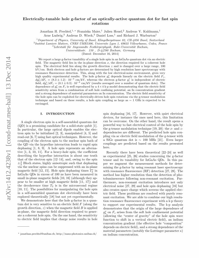
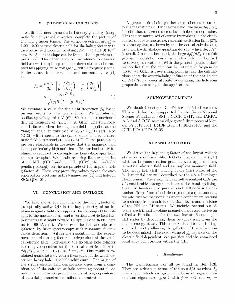
The quantum dots are embedded in the intrinsic re-gion of a p-i-n device. The intrinsic region consists of alayer of self-assembled InGaAs quantum dots located be-tween two highly opaque blocking barriers, in each casean AlAs/GaAs short-period superlattice (16 periods ofAlAs/GaAs 3 nm/1 nm). An electric field Fz of morethan 120 kV/cm can be applied to the QDs [30]. Anetch as deep as the n+ layer is followed by annealingNi/Ge/Au in order to contact the n+ GaAs; 60 nm ofAu deposited directly onto the surface without anneal-ing makes a reasonable contact to the p+ GaAs. Then+ layer is earthed and the electric field is controlled byapplying voltage V to the top Au layer, Fig. 1(a). A split-coil magnet inside a He bath cryostat (4.2 K) provides amagnetic field of 3.00 T in the in-plane direction.
Our experimental scheme involves measuring the fre-quencies of the optical resonances on single QDs withhigh resolution laser spectroscopy. We drive the op-tical transitions with a coherent continuous wave laser(linewidth 1 MHz), collecting the (anti-bunched) reso-nance fluorescence (RF). The RF is separated from re-flected and scattered laser light by a polarization-baseddark-field technique [28]. RF detection is carried outwith a charge-coupled device (CCD) at the output of agrating-based spectrometer (resolution ∼ 40 µeV). Tun-ing is carried out by sweeping the transitions through theconstant frequency laser, exploiting the dc Stark shift(dependence of QD optical frequency on vertical elec-tric field). The typical linewidths are ∼ 5 µeV and inthe spectra presented here, we can determine the peakpositions with a resolution of ±0.2 µeV. We study thenegatively charged exciton, the X1−. This is advanta-geous with respect to the neutral exciton, X0, in that itexhibits no additional fine-structure splitting due to theelectron-hole exchange interaction [31]: the trion spec-trum gives direct access to the electron and hole Zeemanenergies, and hence g-factors. The device does not op-erate in the Coulomb blockade regime where the chargeis precisely controlled. However, we find that X1− dom-inates the optical spectrum in the presence of a smallamount of non resonant laser light (PNR = 0.75 nW).The in-plane magnetic field along x creates a “double”λ-system: the spin-split ground states are both coupled
0.18 0.20 0.22 0.24 0.26 0.28
944.1
944.2
944.3
Voltage (V)
Wav
elen
gth
(nm
)
1.3132
1.3131
1.3130
Ene
rgy
(eV)
(b)
(c) Bin plane = 3T
1 2 3 4
πx 1
∆Eh
∆Ee
X,
X,
X
X
(d)πx 4
πy 2
πy 3
i - GaAs capping layer
n+ - GaAs
SILV
Bx
AlAs/GaAs SPS(30x)
i - GaAsAlAs/GaAs SPS(16x)
AlAs/GaAs SPS(16x)i - GaAs
GaAs substrate
p+ - GaAs
QD
(a)
πyπx
Microscope axiss
Bx
F
p
d
FIG. 1. (a) Layer sequence of the device. On top of the sub-strate a short-period superlattice (SPS) of AlAs/GaAs pe-riods is grown, followed by an n+-doped layer, an intrinsicregion with a second SPS, the quantum dot layer and a thirdSPS, completed with a p+ doped layer on top. On the sam-ple surface a semi-transparent electrode is fabricated, with ahemispherical solid-immersion lens (SIL) positioned on top.(b) Contour plot of the resonance fluorescence (RF) signalas a function of the applied voltage. 1-4 label the four tran-sitions of the charged exciton X1− in an in-plane magneticfield. The transitions are indicated in (c). The color scale isa linear representation of the CCD camera output from back-ground counts (white) to maximum counts 1,200 cts/s (red).(c) The quantum states of a single electron spin in an in-planemagnetic field. ↑,↓ indicate an electron spin, ⇑,⇓ a hole spin.(d) Schematic of the sample orientation in the microscope andof the applied fields.
to the spin-split optically-excited states. The “vertical”transitions in Fig. 1(c) are linearly-polarized along x; the“diagonal” transitions are linearly-polarized along y. xcorresponds to the [100] crystal direction. The laser ispolarized along the “microscope axis” (s/p) and this cor-responds closely to π/4 with respect to the x-axis suchthat the Rabi couplings of all four transitions are similar.
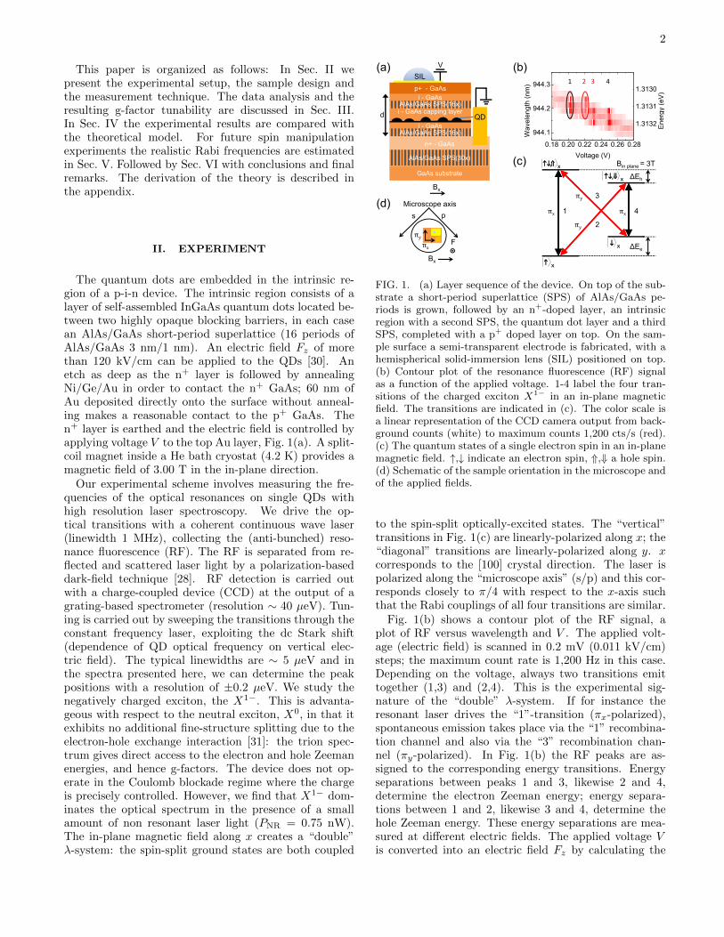
Fig. 1(b) shows a contour plot of the RF signal, aplot of RF versus wavelength and V . The applied volt-age (electric field) is scanned in 0.2 mV (0.011 kV/cm)steps; the maximum count rate is 1,200 Hz in this case.Depending on the voltage, always two transitions emittogether (1,3) and (2,4). This is the experimental sig-nature of the “double” λ-system. If for instance theresonant laser drives the “1”-transition (πx-polarized),spontaneous emission takes place via the “1” recombina-tion channel and also via the “3” recombination chan-nel (πy-polarized). In Fig. 1(b) the RF peaks are as-signed to the corresponding energy transitions. Energyseparations between peaks 1 and 3, likewise 2 and 4,determine the electron Zeeman energy; energy separa-tions between 1 and 2, likewise 3 and 4, determine thehole Zeeman energy. These energy separations are mea-sured at different electric fields. The applied voltage Vis converted into an electric field Fz by calculating the
3
1.20 1.25 1.30 1.350
5001000150020002500
RF
(cou
nts)
0.18 0.20 0.22 0.24 0.26
-0.24 -0.22 -0.200
5001000150020002500
RF
(cou
nts)
Voltage (V)-1.02 -1.00 -0.98
Voltage (V)
ELres = 1.3113 eV, 1.3088 eV
1.3123 eVELres = 1.3138 eV,(a) (b)
(c) (d)
4
(e)
321
20 40 60 80 100 120 140
1.309
1.310
1.311
1.312
1.313
1.314
Ene
rgy
(eV
)
Fz (kV/cm)
1.0 0.5 0.0 -0.5 -1.0Voltage (V)
116 120 124Fz (kV/cm)
28 32 36Fz(kV/cm)
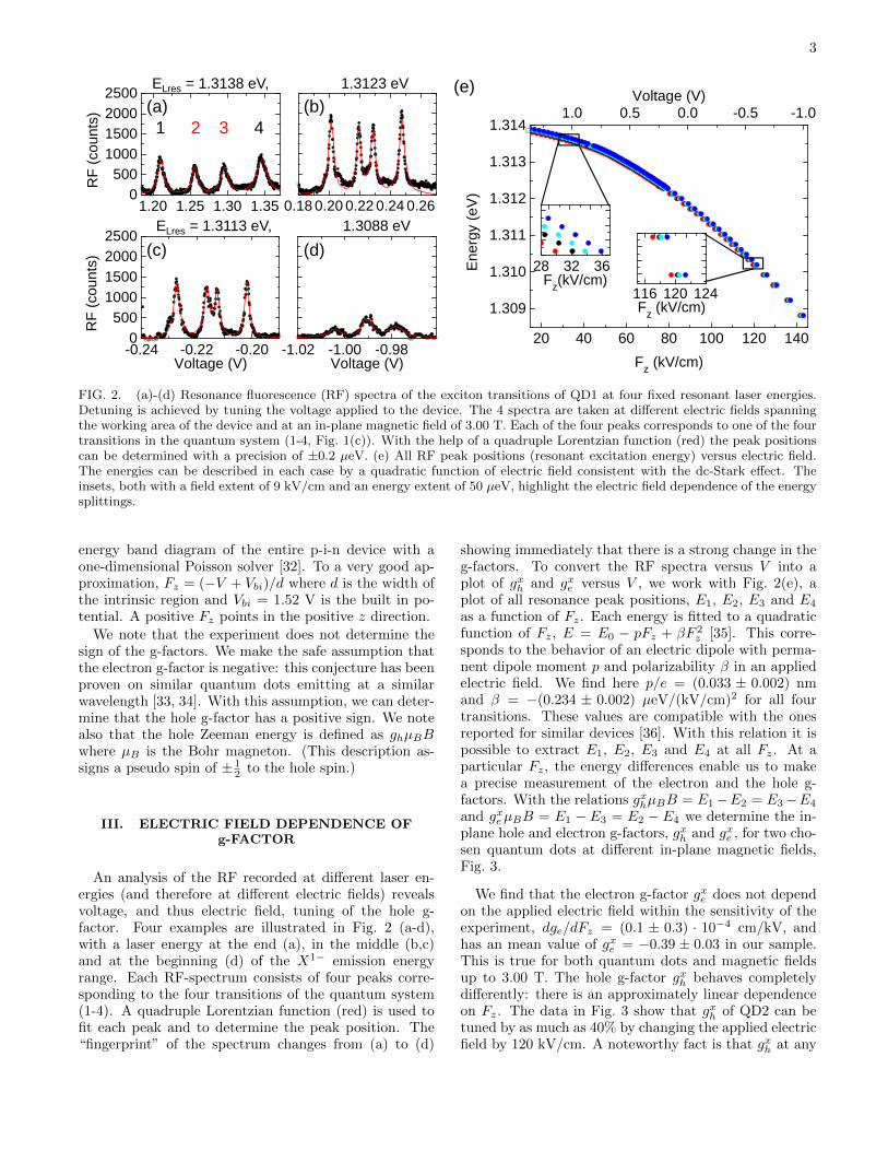
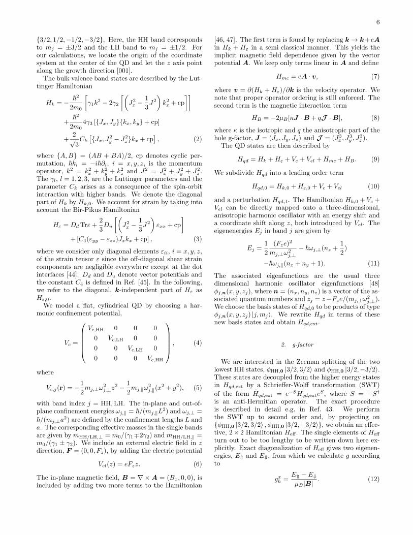
FIG. 2. (a)-(d) Resonance fluorescence (RF) spectra of the exciton transitions of QD1 at four fixed resonant laser energies.Detuning is achieved by tuning the voltage applied to the device. The 4 spectra are taken at different electric fields spanningthe working area of the device and at an in-plane magnetic field of 3.00 T. Each of the four peaks corresponds to one of the fourtransitions in the quantum system (1-4, Fig. 1(c)). With the help of a quadruple Lorentzian function (red) the peak positionscan be determined with a precision of ±0.2 µeV. (e) All RF peak positions (resonant excitation energy) versus electric field.The energies can be described in each case by a quadratic function of electric field consistent with the dc-Stark effect. Theinsets, both with a field extent of 9 kV/cm and an energy extent of 50 µeV, highlight the electric field dependence of the energysplittings.
energy band diagram of the entire p-i-n device with aone-dimensional Poisson solver [32]. To a very good ap-proximation, Fz = (−V + Vbi)/d where d is the width ofthe intrinsic region and Vbi = 1.52 V is the built in po-tential. A positive Fz points in the positive z direction.
We note that the experiment does not determine thesign of the g-factors. We make the safe assumption thatthe electron g-factor is negative: this conjecture has beenproven on similar quantum dots emitting at a similarwavelength [33, 34]. With this assumption, we can deter-mine that the hole g-factor has a positive sign. We notealso that the hole Zeeman energy is defined as ghµBBwhere µB is the Bohr magneton. (This description as-signs a pseudo spin of ± 1
2 to the hole spin.)
III. ELECTRIC FIELD DEPENDENCE OFg-FACTOR
An analysis of the RF recorded at different laser en-ergies (and therefore at different electric fields) revealsvoltage, and thus electric field, tuning of the hole g-factor. Four examples are illustrated in Fig. 2 (a-d),with a laser energy at the end (a), in the middle (b,c)and at the beginning (d) of the X1− emission energyrange. Each RF-spectrum consists of four peaks corre-sponding to the four transitions of the quantum system(1-4). A quadruple Lorentzian function (red) is used tofit each peak and to determine the peak position. The“fingerprint” of the spectrum changes from (a) to (d)
showing immediately that there is a strong change in theg-factors. To convert the RF spectra versus V into aplot of gxh and gxe versus V , we work with Fig. 2(e), aplot of all resonance peak positions, E1, E2, E3 and E4
as a function of Fz. Each energy is fitted to a quadraticfunction of Fz, E = E0 − pFz + βF 2
z [35]. This corre-sponds to the behavior of an electric dipole with perma-nent dipole moment p and polarizability β in an appliedelectric field. We find here p/e = (0.033 ± 0.002) nmand β = −(0.234 ± 0.002) µeV/(kV/cm)2 for all fourtransitions. These values are compatible with the onesreported for similar devices [36]. With this relation it ispossible to extract E1, E2, E3 and E4 at all Fz. At aparticular Fz, the energy differences enable us to makea precise measurement of the electron and the hole g-factors. With the relations gxhµBB = E1−E2 = E3−E4
and gxeµBB = E1 − E3 = E2 − E4 we determine the in-plane hole and electron g-factors, gxh and gxe , for two cho-sen quantum dots at different in-plane magnetic fields,Fig. 3.
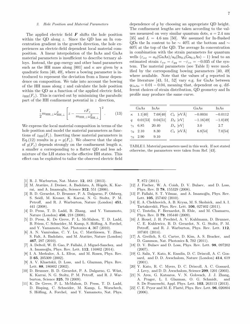
We find that the electron g-factor gxe does not dependon the applied electric field within the sensitivity of theexperiment, dge/dFz = (0.1 ± 0.3) · 10−4 cm/kV, andhas an mean value of gxe = −0.39 ± 0.03 in our sample.This is true for both quantum dots and magnetic fieldsup to 3.00 T. The hole g-factor gxh behaves completelydifferently: there is an approximately linear dependenceon Fz. The data in Fig. 3 show that gxh of QD2 can betuned by as much as 40% by changing the applied electricfield by 120 kV/cm. A noteworthy fact is that gxh at any
4
20 40 60 80 100 120 1400.0
0.1
0.2
0.3
0.4
0.5g-
fact
or
Fz (kV/cm)
QD1
QD2
QD2
|g||e|
g||h
QD1
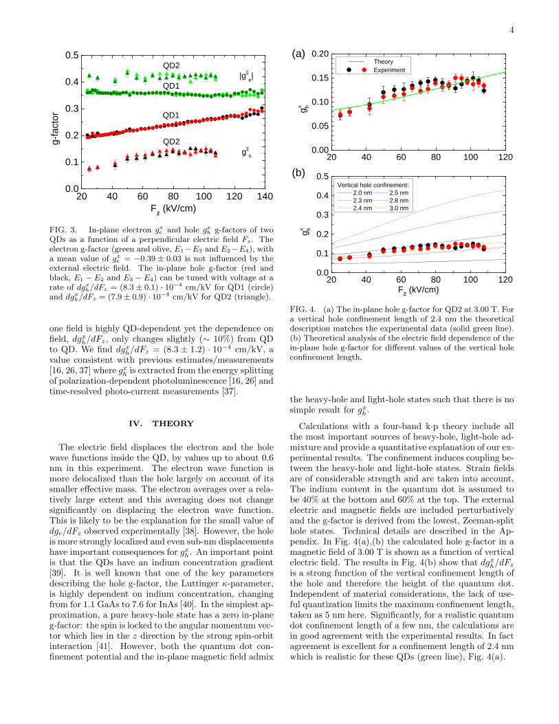
FIG. 3. In-plane electron gxe and hole gxh g-factors of twoQDs as a function of a perpendicular electric field Fz. Theelectron g-factor (green and olive, E1−E3 and E2−E4), witha mean value of gxe = −0.39 ± 0.03 is not influenced by theexternal electric field. The in-plane hole g-factor (red andblack, E1 − E2 and E3 − E4) can be tuned with voltage at arate of dgxh/dFz = (8.3 ± 0.1) · 10−4 cm/kV for QD1 (circle)and dgxh/dFz = (7.9± 0.9) · 10−4 cm/kV for QD2 (triangle).
one field is highly QD-dependent yet the dependence onfield, dgxh/dFz, only changes slightly (∼ 10%) from QDto QD. We find dgxh/dFz = (8.3 ± 1.2) · 10−4 cm/kV, avalue consistent with previous estimates/measurements[16, 26, 37] where gxh is extracted from the energy splittingof polarization-dependent photoluminescence [16, 26] andtime-resolved photo-current measurements [37].
IV. THEORY
The electric field displaces the electron and the holewave functions inside the QD, by values up to about 0.6nm in this experiment. The electron wave function ismore delocalized than the hole largely on account of itssmaller effective mass. The electron averages over a rela-tively large extent and this averaging does not changesignificantly on displacing the electron wave function.This is likely to be the explanation for the small value ofdge/dFz observed experimentally [38]. However, the holeis more strongly localized and even sub-nm displacementshave important consequences for gxh. An important pointis that the QDs have an indium concentration gradient[39]. It is well known that one of the key parametersdescribing the hole g-factor, the Luttinger κ-parameter,is highly dependent on indium concentration, changingfrom for 1.1 GaAs to 7.6 for InAs [40]. In the simplest ap-proximation, a pure heavy-hole state has a zero in-planeg-factor: the spin is locked to the angular momentum vec-tor which lies in the z direction by the strong spin-orbitinteraction [41]. However, both the quantum dot con-finement potential and the in-plane magnetic field admix
(a)
(b)20 40 60 80 100 120
0.00
0.05
0.10
0.15
0.20
Theory Experiment
gx h
20 40 60 80 100 1200.0
0.1
0.2
0.3
0.4
0.5
Vertical hole confinement: 2.0 nm 2.5 nm 2.3 nm 2.8 nm 2.4 nm 3.0 nm
gx h
Fz (kV/cm)
az=2.4nm (Warb PRB 02 2.6nm (el 3.4nm)) Lxy=4.6nm ( hole 3nm (el 5nm) Brian APL 07)εxx= ‐0.035 (In conc med x= 0.5) In 0.4‐0.6 (justified Arne: pure InAs after annealing!)
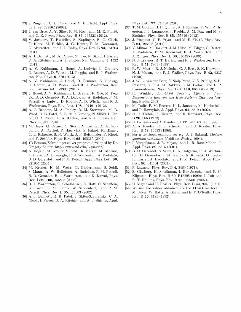
FIG. 4. (a) The in-plane hole g-factor for QD2 at 3.00 T. Fora vertical hole confinement length of 2.4 nm the theoreticaldescription matches the experimental data (solid green line).(b) Theoretical analysis of the electric field dependence of thein-plane hole g-factor for different values of the vertical holeconfinement length.
the heavy-hole and light-hole states such that there is nosimple result for gxh.
Calculations with a four-band k·p theory include allthe most important sources of heavy-hole, light-hole ad-mixture and provide a quantitative explanation of our ex-perimental results. The confinement induces coupling be-tween the heavy-hole and light-hole states. Strain fieldsare of considerable strength and are taken into account.The indium content in the quantum dot is assumed tobe 40% at the bottom and 60% at the top. The externalelectric and magnetic fields are included perturbativelyand the g-factor is derived from the lowest, Zeeman-splithole states. Technical details are described in the Ap-pendix. In Fig. 4(a),(b) the calculated hole g-factor in amagnetic field of 3.00 T is shown as a function of verticalelectric field. The results in Fig. 4(b) show that dgxh/dFz
is a strong function of the vertical confinement length ofthe hole and therefore the height of the quantum dot.Independent of material considerations, the lack of use-ful quantization limits the maximum confinement length,taken as 5 nm here. Significantly, for a realistic quantumdot confinement length of a few nm, the calculations arein good agreement with the experimental results. In factagreement is excellent for a confinement length of 2.4 nmwhich is realistic for these QDs (green line), Fig. 4(a).
5
V. g-TENSOR MODULATION
Additional measurements in Faraday geometry (mag-netic field in growth direction) complete the picture ofthe hole g-factor tensor. The values we extract are gzh =1.22± 0.02 at zero electric field for the hole g-factor withan electric field dependence of dgzh/dFz = (4.1±1.0)·10−3
cm/kV. A similar slope can be found also in previous re-ports [25]. The dependency of the g-tensor on electricfield allows the spin-up and spin-down states to be cou-pled by applying an ac voltage Vac with a frequency equalto the Larmor frequency. The resulting coupling fR [21]is,
fR =µBVac
2h
[1
g‖
(∂g‖
∂Vg
)− 1
g⊥
(∂g⊥∂Vg
)]×
g‖g⊥B‖B⊥√(g‖B‖
)2+(g⊥B⊥
)2 . (1)
We estimate a value for the Rabi frequency fR basedon our results for the hole g-factor. We consider anoscillating voltage of 1 V (67 kV/cm) and a maximumdriving frequency of fLarmor= 20 GHz. The spin rota-tion is fastest when the magnetic field is applied at the“magic” angle, in this case at 20.7◦ (QD1) and 14.5◦
(QD2) with respect to the (x, y) plane. The total mag-netic field corresponds to 3.2 (4.6) T. These parametersare very reasonable in the sense that the magnetic fieldis not particularly high and that it lies predominantly in-plane, as required to decouple the heavy-hole spin fromthe nuclear spins. We obtain resulting Rabi frequenciesof 350 MHz (QD1) and 1.1 GHz (QD2), the result de-pending strongly on the magnitude of the in-plane holeg-factor gxh. These very promising values exceed the onesreported for electrons in InSb nanowires [42] and holes inSiGe QDs [21].
VI. CONCLUSION AND OUTLOOK
We have shown the tunability of the hole g-factor ofan optically active QD in the key geometry of an in-plane magnetic field (to suppress the coupling of the holespin to the nuclear spins) and a vertical electric field (ex-perimentally straightforward to apply large fields, hereup to 100 kV/cm). We derived the hole and electrong-factors by laser spectroscopy with resonance fluores-cence detection. Within the resolution of the experi-ment, the electron g-factor is independent of the verti-cal electric field. Conversely, the in-plane hole g-factoris strongly dependent on the vertical electric field withdgxh/dFz = (8.3 ± 1.2) · 10−4 cm/kV. This result is ex-plained quantitatively with a theoretical model which de-scribes heavy-hole light-hole admixture. The origin ofthe strong electric field dependence arises from a com-bination of the softness of hole confining potential, anindium concentration gradient and a strong dependenceof material parameters on indium concentration.
A quantum dot hole spin becomes coherent in an in-plane magnetic field. On the one hand, the large dgxh/dFz
implies that charge noise results in hole spin dephasing.This can be minimized of course by working in the clean-material, low-temperature, resonant-excitation limit [27].Another option, as shown by the theoretical calculations,is to work with shallow quantum dots for which dgxh/dFz
is small. On the other hand, the large dgxh/dFz is useful:g-tensor modulation via an ac electric field can be usedto drive spin rotations. With the present quantum dotswe predict that the spin can be rotated at frequenciesup to ∼ 1 GHz. An overriding point is that the calcula-tions show the overwhelming influence of the dot heighton dgxh/dFz, a powerful route to designing the hole spinproperties according to the application.
ACKNOWLEDGMENTS
We thank Christoph Kloeffel for helpful discussions.This work has been supported by the Swiss NationalScience Foundation (SNF), NCCR QSIT, and IARPA.A.L. and A.D.W. acknowledge gratefully support of Mer-cur Pr-2013-0001, BMBF-Q.com-H 16KIS0109, and theDFH/UFA CDFA-05-06.
APPENDIX: THEORY
We derive the in-plane g-factor of the lowest valencestates in a self-assembled InGaAs quantum dot (QD)with an In concentration gradient with applied fields,a vertical electric field and an in-plane magnetic field.The heavy-hole (HH) and light-hole (LH) states of thebulk material are well described by the 4 × 4 LuttingerHamiltonian. The strain fields in self-assembled QDs areof considerable strength and affect the band splitting.Strain is therefore incorporated via the Bir-Pikus Hamil-tonian. To go from a bulk description to a quantum dot,we add three-dimensional harmonic confinement leadingto a change from bands to quantized levels and a mixingof the HH and LH states. We include external out-of-plane electric and in-plane magnetic fields and derive aneffective Hamiltonian for the two lowest, Zeeman-splitHH states by decoupling them perturbatively from thehigher energy states. This effective Hamiltonian is diag-onalized exactly allowing the g-factor of this subsystemto be determined. The exact value of gxh depends on theelectric field-dependent hole position and the associatedlocal alloy composition within the QD.
1. Hamiltonian
The Hamiltonians can all be found in Ref. [43].They are written in terms of the spin-3/2 matrices Ji,i = x, y, z, which are given in a basis of angular mo-mentum eigenstates |j,mj〉 with j = 3/2 and mj =
6
{3/2, 1/2,−1/2,−3/2}. Here, the HH band correspondsto mj = ±3/2 and the LH band to mj = ±1/2. Forour calculations, we locate the origin of the coordinatesystem at the center of the QD and let the z axis pointalong the growth direction [001].
The bulk valence band states are described by the Lut-tinger Hamiltonian
Hk = − ~2
2m0
[γ1k
2 − 2γ2
[(J2x −
1
3J2
)k2x + cp
]]+
~2
2m04γ3 [{Jx, Jy}{kx, ky}+ cp]
+2√3Ck
[{Jx, J2
y − J2z }kx + cp
], (2)
where {A,B} = (AB + BA)/2, cp denotes cyclic per-mutation, ~ki = −i~∂i, i = x, y, z, is the momentumoperator, k2 = k2
x + k2y + k2
z and J2 = J2x + J2
y + J2z .
The γl, l = 1, 2, 3, are the Luttinger parameters and theparameter Ck arises as a consequence of the spin-orbitinteraction with higher bands. We denote the diagonalpart of Hk by Hk,0. We account for strain by taking intoaccount the Bir-Pikus Hamiltonian
Hε = Dd Trε+2
3Du
[(J2x −
1
3J2
)εxx + cp
]+ [C4(εyy − εzz)Jxkx + cp] , (3)
where we consider only diagonal elements εii, i = x, y, z,of the strain tensor ε since the off-diagonal shear straincomponents are negligible everywhere except at the dotinterfaces [44]. Dd and Du denote vector potentials andthe constant C4 is defined in Ref. [45]. In the following,we refer to the diagonal, k-independent part of Hε asHε,0.
We model a flat, cylindrical QD by choosing a har-monic confinement potential,
Vc =
Vc,HH 0 0 0
0 Vc,LH 0 0
0 0 Vc,LH 0
0 0 0 Vc,HH
, (4)
where
Vc,j(r) = −1
2mj,⊥ω
2j,⊥z
2 − 1
2mj,‖ω
2j,‖(x
2 + y2), (5)
with band index j = HH,LH. The in-plane and out-of-plane confinement energies ωj,‖ = ~/(mj,‖L
2) and ωj,⊥ =
~/(mj,⊥a2) are defined by the confinement lengths L and
a. The corresponding effective masses in the single bandsare given by mHH/LH,⊥ = m0/(γ1∓2γ2) and mHH/LH,‖ =m0/(γ1 ± γ2). We include an external electric field in zdirection, F = (0, 0, Fz), by adding the electric potential
Vel(z) = eFzz. (6)
The in-plane magnetic field, B = ∇×A = (Bx, 0, 0), isincluded by adding two more terms to the Hamiltonian
[46, 47]. The first term is found by replacing k→ k+eAin Hk + Hε in a semi-classical manner. This yields theimplicit magnetic field dependence given by the vectorpotential A. We keep only terms linear in A and define
Hmc = eA · v, (7)
where v = ∂(Hk + Hε)/∂k is the velocity operator. Wenote that proper operator ordering is still enforced. Thesecond term is the magnetic interaction term
HB = −2µB [κJ ·B + qJ ·B], (8)
where κ is the isotropic and q the anisotropic part of thehole g-factor, J = (Jx, Jy, Jz) and J = (J3
x , J3y , J
3z ).
The QD states are then described by
Hqd = Hk +Hε + Vc + Vel +Hmc +HB . (9)
We subdivide Hqd into a leading order term
Hqd,0 = Hk,0 +Hε,0 + Vc + Vel (10)
and a perturbation Hqd,1. The Hamiltonian Hk,0 + Vc +Vel can be directly mapped onto a three-dimensional,anisotropic harmonic oscillator with an energy shift anda coordinate shift along z, both introduced by Vel. Theeigenenergies Ej in band j are given by
Ej =1
2
(Fze)2
mj,⊥ω2j,⊥− ~ωj,⊥(nz +
1
2)
−~ωj,‖(nx + ny + 1). (11)
The associated eigenfunctions are the usual threedimensional harmonic oscillator eigenfunctions [48]φj,n(x, y, zj), where n = (nx, ny, nz) is a vector of the as-sociated quantum numbers and zj = z−Fze/(mj,⊥ω
2j,⊥).
We choose the basis states of Hqd,0 to be products of typeφj,n(x, y, zj) |j,mj〉. We rewrite Hqd in terms of thesenew basis states and obtain Hqd,ext.
2. g-factor
We are interested in the Zeeman splitting of the twolowest HH states, φHH,0 |3/2, 3/2〉 and φHH,0 |3/2,−3/2〉.These states are decoupled from the higher energy statesin Hqd,ext by a Schrieffer-Wolff transformation (SWT)
of the form Hqd,ext = e−SHqd,exteS , where S = −S†
is an anti-Hermitian operator. The exact procedureis described in detail e.g. in Ref. 43. We performthe SWT up to second order and, by projecting on{φHH,0 |3/2, 3/2〉 , φHH,0 |3/2,−3/2〉}, we obtain an effec-tive, 2× 2 Hamiltonian Heff. The single elements of Heff
turn out to be too lengthy to be written down here ex-plicitly. Exact diagonalization of Heff gives two eigenen-ergies, E⇑ and E⇓, from which we calculate g accordingto
gxh =E⇑ − E⇓µB |B|
. (12)
7
3. Hole Position and Material Parameters
The applied electric field F shifts the hole positionwithin the QD along z. Since the QD has an In con-centration gradient in the growth direction, the hole ex-periences an electric-field dependent local material com-position. A linear interpolation of the InAs and GaAsmaterial parameters is insufficient to describe ternary al-loys. Instead, the gap energy and other band parameterssuch as the HH mass along [001] and κ are given by aquadratic form [40, 49], where a bowing parameter is in-troduced to represent the deviation from a linear depen-dence on composition. We take into account the bowingof the HH mass along z and calculate the hole positionwithin the QD as a function of the applied electric field,zHH(Fz). This is carried out by minimizing the parabolicpart of the HH confinement potential in z direction,
1
2mHH,⊥ω
2HH,⊥
[z − eFz
mHH,⊥ω2HH,⊥
]2
. (13)
We express the local material composition in terms of thehole position and model the material parameters as func-tions of zHH(Fz). Inserting these material parameters inEq.(12) results in g = g(Fz). We observe that the slopeof g(Fz) depends strongly on the confinement length a,a smaller a corresponding to a flatter QD and less ad-mixture of the LH states to the effective HH states. Thiseffect can be exploited to tailor the observed electric field
dependence of g by choosing an appropriate QD height.The confinement lengths are taken according to the val-ues measured on very similar quantum dots, a = 2.4 nm[35] and L = 4.6 nm [50]. We assumed for In-flushedQDs the In content to be ∼ 40% at the bottom and ∼60% at the top of the QD. The average In concentrationin combination with the strain parameters for quantumwells (εxx = a0(GaAs)/a0(In0.5Ga0.5As) − 1) lead to anestimated strain εxx = εyy = −εzz = −0.035 of the sys-tem. The material parameters (see Table I) were mod-ified by the corresponding bowing parameters [40, 49]where available. Note that the values of q reported inthe literature [43, 51, 52] vary e.g. for GaAs betweenqGaAs = 0.01 − 0.04, meaning that, dependent on q, dif-ferent choices of strain distribution, QD geometry and Inprofile may produce the same curve.
GaAs InAs GaAs InAs
κ 1.1[40] 7.68[40] Ck [eVA] −0.0034 −0.0112
q 0.01[53] 0.04[51] Dd [eV] −1.16[49] −1.0[49]
γ1 6.85 20.40 Du [eV] 3.0 2.7
γ2 2.10 8.30 C4 [eVA] 6.8[54] 7.0[54]
γ3 2.90 9.10
TABLE I. Material parameters used in this work. If not statedotherwise, the parameters were taken from Ref. [43].
[1] R. J. Warburton, Nat. Mater. 12, 483 (2013).[2] M. Atature, J. Dreiser, A. Badolato, A. Hogele, K. Kar-
rai, and A. Imamoglu, Science 312, 551 (2006).[3] B. D. Gerardot, D. Brunner, P. A. Dalgarno, P. Ohberg,
S. Seidl, M. Kroner, K. Karrai, N. G. Stoltz, P. M.Petroff, and R. J. Warburton, Nature (London) 451,441 (2008).
[4] D. Press, T. D. Ladd, B. Zhang, and Y. Yamamoto,Nature (London) 456, 218 (2008).
[5] D. Press, K. De Greve, P. L. McMahon, T. D. Ladd,B. Friess, C. Schneider, M. Kamp, S. Hofling, A. Forchel,and Y. Yamamoto, Nat. Photonics 4, 367 (2010).
[6] A. N. Vamivakas, C. Y. Lu, C. Matthiesen, Y. Zhao,S. Falt, A. Badolato, and M. Atature, Nature (London)467, 297 (2010).
[7] A. Delteil, W. B. Gao, P. Fallahi, J. Miguel-Sanchez, andA. Imamoglu, Phys. Rev. Lett. 112, 116802 (2014).
[8] I. A. Merkulov, A. L. Efros, and M. Rosen, Phys. Rev.B 65, 205309 (2002).
[9] A. V. Khaetskii, D. Loss, and L. Glazman, Phys. Rev.Lett. 88, 186802 (2002).
[10] D. Brunner, B. D. Gerardot, P. A. Dalgarno, G. Wust,K. Karrai, N. G. Stoltz, P. M. Petroff, and R. J. War-burton, Science 325, 70 (2009).
[11] K. De Greve, P. L. McMahon, D. Press, T. D. Ladd,D. Bisping, C. Schneider, M. Kamp, L. Worschech,S. Hofling, A. Forchel, and Y. Yamamoto, Nat. Phys.
7, 872 (2011).[12] J. Fischer, W. A. Coish, D. V. Bulaev, and D. Loss,
Phys. Rev. B 78, 155329 (2008).[13] P. Fallahi, S. T. Yilmaz, and A. Imamoglu, Phys. Rev.
Lett. 105, 257402 (2010).[14] E. A. Chekhovich, A. B. Krysa, M. S. Skolnick, and A. I.
Tartakovskii, Phys. Rev. Lett. 106, 027402 (2011).[15] C. Testelin, F. Bernardot, B. Eble, and M. Chamarro,
Phys. Rev. B 79, 195440 (2009).[16] J. Houel, J. H. Prechtel, A. V. Kuhlmann, D. Brunner,
C. E. Kuklewicz, B. D. Gerardot, N. G. Stoltz, P. M.Petroff, and R. J. Warburton, Phys. Rev. Lett. 112,107401 (2014).
[17] A. Greilich, S. G. Carter, D. Kim, A. S. Bracker, andD. Gammon, Nat. Photonics 5, 702 (2011).
[18] D. V. Bulaev and D. Loss, Phys. Rev. Lett. 98, 097202(2007).
[19] G. Salis, Y. Kato, K. Ensslin, D. C. Driscoll, A. C. Gos-sard, and D. D. Awschalom, Nature (London) 414, 619(2001).
[20] Y. Kato, R. C. Myers, D. C. Driscoll, A. C. Gossard,J. Levy, and D. D. Awschalom, Science 299, 1201 (2003).
[21] N. Ares, G. Katsaros, V. N. Golovach, J. J. Zhang,A. Prager, L. I. Glazman, O. G. Schmidt, andS. De Franceschi, Appl. Phys. Lett. 103, 263113 (2013).
[22] C. E. Pryor and M. E. Flatte, Phys. Rev. Lett. 96, 026804(2006).
8
[23] J. Pingenot, C. E. Pryor, and M. E. Flatte, Appl. Phys.Lett. 92, 222502 (2008).
[24] J. van Bree, A. Y. Silov, P. M. Koenraad, M. E. Flatte,and C. E. Pryor, Phys. Rev. B 85, 165323 (2012).
[25] V. Jovanov, T. Eissfeller, S. Kapfinger, E. C. Clark,F. Klotz, M. Bichler, J. G. Keizer, P. M. Koenraad,G. Abstreiter, and J. J. Finley, Phys. Rev. B 83, 161303(2011).
[26] A. J. Bennett, M. A. Pooley, Y. Cao, N. Skold, I. Farrer,D. A. Ritchie, and A. J. Shields, Nat. Commun. 4, 1522(2013).
[27] A. V. Kuhlmann, J. Houel, A. Ludwig, L. Greuter,D. Reuter, A. D. Wieck, , M. Poggio, and R. J. Warbur-ton, Nat. Phys. 9, 570 (2013).
[28] A. V. Kuhlmann, J. Houel, D. Brunner, A. Ludwig,D. Reuter, A. D. Wieck, and R. J. Warburton, Rev.Sci. Instrum. 84, 073905 (2013).
[29] J. Houel, A. V. Kuhlmann, L. Greuter, F. Xue, M. Pog-gio, B. D. Gerardot, P. A. Dalgarno, A. Badolato, P. M.Petroff, A. Ludwig, D. Reuter, A. D. Wieck, and R. J.Warburton, Phys. Rev. Lett. 108, 107401 (2012).
[30] A. J. Bennett, M. A. Pooley, R. M. Stevenson, M. B.Ward, R. B. Patel, A. B. de la Giroday, N. Skold, I. Far-rer, C. A. Nicoll, D. A. Ritchie, and A. J. Shields, Nat.Phys. 6, 947 (2010).
[31] M. Bayer, G. Ortner, O. Stern, A. Kuther, A. A. Gor-bunov, A. Forchel, P. Hawrylak, S. Fafard, K. Hinzer,T. L. Reinecke, S. N. Walck, J. P. Reithmaier, F. Klopf,and F. Schafer, Phys. Rev. B 65, 195315 (2002).
[32] 1D Poisson/Schrodinger solver program developed by Dr.Gregory Snider, http://www.nd.edu/∼gsnider/.
[33] A. Hogele, M. Kroner, S. Seidl, K. Karrai, M. Atature,J. Dreiser, A. Imamoglu, R. J. Warburton, A. Badolato,B. D. Gerardot, and P. M. Petroff, Appl. Phys. Lett. 86,221905 (2005).
[34] M. Kroner, K. M. Weiss, B. Biedermann, S. Seidl,S. Manus, A. W. Holleitner, A. Badolato, P. M. Petroff,B. D. Gerardot, R. J. Warburton, and K. Karrai, Phys.Rev. Lett. 100, 156803 (2008).
[35] R. J. Warburton, C. Schulhauser, D. Haft, C. Schaflein,K. Karrai, J. M. Garcia, W. Schoenfeld, and P. M.Petroff, Phys. Rev. B 65, 113303 (2002).
[36] A. J. Bennett, R. B. Patel, J. Skiba-Szymanska, C. A.Nicoll, I. Farrer, D. A. Ritchie, and A. J. Shields, Appl.
Phys. Lett. 97, 031104 (2010).[37] T. M. Godden, J. H. Quilter, A. J. Ramsay, Y. Wu, P. Br-
ereton, I. J. Luxmoore, J. Puebla, A. M. Fox, and M. S.Skolnick, Phys. Rev. B 85, 155310 (2012).
[38] J. Pingenot, C. E. Pryor, and M. E. Flatte, Phys. Rev.B 84, 195403 (2011).
[39] V. Mlinar, M. Bozkurt, J. M. Ulloa, M. Ediger, G. Bester,A. Badolato, P. M. Koenraad, R. J. Warburton, andA. Zunger, Phys. Rev. B 80, 165425 (2009).
[40] N. J. Traynor, R. T. Harley, and R. J. Warburton, Phys.Rev. B 51, 7361 (1995).
[41] R. W. Martin, R. J. Nicholas, G. J. Rees, S. K. Haywood,N. J. Mason, and P. J. Walker, Phys. Rev. B 42, 9237(1990).
[42] J. W. G. van den Berg, S. Nadj-Perge, V. S. Pribiag, S. R.Plissard, E. P. A. M. Bakkers, S. M. Frolov, and L. P.Kouwenhoven, Phys. Rev. Lett. 110, 066806 (2013).
[43] R. Winkler, Spin-Orbit Coupling Effects in Two-Dimensional Electron and Hole Systems (Springer Ver-lag, Berlin, 2003).
[44] M. Tadic, F. M. Peeters, K. L. Janssens, M. Korkusiski,and P. Hawrylak, J. Appl. Phys. 92, 5819 (2002).
[45] H. R. Trebin, U. Rossler, and R. Ranvaud, Phys. Rev.B 20, 686 (1979).
[46] E. Ivchenko and A. Kiselev, JETP Lett. 67, 43 (1998).[47] A. A. Kiselev, E. L. Ivchenko, and U. Rossler, Phys.
Rev. B 58, 16353 (1998).[48] For a textbook example see e.g. J. J. Sakurai, Modern
quantum mechanics (Addison-Wesley, 1994).[49] I. Vurgaftman, J. R. Meyer, and L. R. Ram-Mohan, J.
Appl. Phys. 89, 5815 (2001).[50] B. D. Gerardot, S. Seidl, P. A. Dalgarno, R. J. Warbur-
ton, D. Granados, J. M. Garcia, K. Kowalik, O. Krebs,K. Karrai, A. Badolato, and P. M. Petroff, Appl. Phys.Lett. 90, 041101 (2007).
[51] P. Lawaetz, Phys. Rev. B 4, 3460 (1971).[52] S. Glasberg, H. Shtrikman, I. Bar-Joseph, and P. C.
Klipstein, Phys. Rev. B 60, R16295 (1999); I. Toft andR. T. Phillips, Phys. Rev. B 76, 033301 (2007).
[53] H. Mayer and U. Rossler, Phys. Rev. B 44, 9048 (1991).[54] We use the values obtained via the LCAO method in
M. Silver, W. Batty, A. Ghiti, and E. P. O’Reilly, Phys.Rev. B 46, 6781 (1992).
Related Documents