1 Electrically driven photonic crystal nanocavity devices Gary Shambat, Bryan Ellis, Jan Petykiewicz, Marie A. Mayer, Arka Majumdar, Tomas Sarmiento, James Harris, Eugene E. Haller, and Jelena Vuˇ ckovi´ c Abstract—Interest in photonic crystal nanocavities is fueled by advances in device performance, particularly in the development of low-threshold laser sources. Effective electrical control of high performance photonic crystal lasers has thus far remained elusive due to the complexities associated with current injection into cav- ities. A fabrication procedure for electrically pumping photonic crystal membrane devices using a lateral p-i-n junction has been developed and is described in this work. We have demonstrated electrically pumped lasing in our junctions with a threshold of 181 nA at 50K - the lowest threshold ever demonstrated in an electrically pumped laser. At room temperature we find that our devices behave as single-mode light-emitting diodes (LEDs), which when directly modulated, have an ultrafast electrical response up to 10 GHz corresponding to less than 1 fJ/bit energy operation - the lowest for any optical transmitter. In addition, we have demonstrated electrical pumping of photonic crystal nanobeam LEDs, and have built fiber taper coupled electro-optic modulators. Fiber-coupled photodetectors based on two-photon absorption are also demonstrated as well as multiply integrated components that can be independently electrically controlled. The presented electrical injection platform is a major step forward in providing practical low power and integrable devices for on-chip photonics. Index Terms—Photonic bandgap materials, cavity resonators, lasers, light-emitting diodes, modulation, electro-optic modula- tion, photodetectors, quantum dots I. I NTRODUCTION P HOTONIC crystal (PC) nanocavities have been the focus of intense research in recent years as these engineered nanostructures have opened the door for novel physics and device applications. A tremendous amount of progress has been made both in optimizing cavity properties such as the quality (Q) factor [1]–[3] and mode volume as well as in de- veloping interesting applications that are intrinsically enabled through a nanoscale dielectric form factor [4]–[6]. Early work in this field showed that localized defect modes can be created by perturbing the periodicity of a photonic lattice, creating highly customizable nanocavities with simple control over mode field patterns, radiation profiles, spectral positioning, and photon lifetime [7], [8]. The first experimental demonstration of a PC cavity laser began a wave of research in active G. Shambat, B. Ellis, J. Petykiewicz, Arka Majumdar, Tomas Sarmiento, James Harris, and J. Vuˇ ckovi´ c are with the Department of Electri- cal Engineering, Stanford University, Stanford, CA 94305 USA (e- mail: [email protected]; [email protected]; [email protected]; [email protected]; [email protected]; [email protected]; [email protected]). M. A. Mayer and E. E. Haller are with the Materials Sciences Division, Lawrence Berkeley National Laboratory, Berkeley, CA 94720 USA (e-mail: [email protected]; [email protected] photonic crystal cavity devices [9]. PC nanocavity lasers have advanced remarkably and now represent the state of the art in low-threshold lasers [10]. In such high Q-factor and small mode-volume cavities the Purcell factor can be quite high, reducing the lasing threshold and increasing the modulation rate [11]. Optically pumped PC nanocavity lasers have been demonstrated to have thresholds of only a few nW, high output powers, and modulation rates exceeding 100 GHz [12]–[14]. Furthermore, they can operate in continuous wave mode at room temperature and can be efficiently coupled to passive waveguides for optoelectronic integrated circuit applications [15], [16]. Although sophisticated PC lasers and active devices have been developed, their corresponding electrical control has lagged tremendously. Because of the challenges associated with electrical pumping of photonic crystal membranes, all of the aforementioned laser demonstrations relied on impractical optical pumping. There has been one previous demonstration of an electrically pumped photonic crystal laser using a vertical p-i-n junction grown within the semiconductor membrane [17]. A current post is used to inject carriers into the cavity region; however the current post limits the quality factor of the cavity, restricts the choice of the cavity design, and requires a complicated fabrication procedure [18]. In addition, a high threshold current of 260 μA was observed, significantly higher than in optically pumped PC devices and even exceeding that of good vertical-cavity surface-emitting lasers (VCSELs) [19]. Other groups have used similar vertical p-i-n designs for electrical pumping of PC LEDs but have not been able to resolve the complications associated with this inefficient injection platform [20], [21]. Due to the limited current spreading ability of the thin conductive layers, most of the electroluminescence (EL) is not coupled to the cavity, wasting electrical power and heating the device. We have therefore devised a new method for electrical control of photonic crystal cavities employing a lateral p-i- n junction (shown schematically in Fig. 1(a) and visualized in the SEM in Fig. 1(b)) [22], [23]. The geometry inherent to 2D photonic crystal membranes lends itself more easily to lateral current injection defined by ion implanted p- and n- type regions. This device architecture has a simple and flexible fabrication procedure with high control over the current flow. In addition, arbitrary PC cavity designs with high Q-factors can be used along with coupling waveguides for efficient light extraction. Moreover, doping is introduced only in desired areas, enabling efficient integration of active and passive devices (as opposed to vertical p-i-n junctions where the doped arXiv:1201.0964v1 [physics.optics] 4 Jan 2012

Welcome message from author
This document is posted to help you gain knowledge. Please leave a comment to let me know what you think about it! Share it to your friends and learn new things together.
Transcript

1
Electrically driven photonic crystal nanocavitydevices
Gary Shambat, Bryan Ellis, Jan Petykiewicz, Marie A. Mayer, Arka Majumdar, Tomas Sarmiento, James Harris,Eugene E. Haller, and Jelena Vuckovic
Abstract—Interest in photonic crystal nanocavities is fueled byadvances in device performance, particularly in the developmentof low-threshold laser sources. Effective electrical control of highperformance photonic crystal lasers has thus far remained elusivedue to the complexities associated with current injection into cav-ities. A fabrication procedure for electrically pumping photoniccrystal membrane devices using a lateral p-i-n junction has beendeveloped and is described in this work. We have demonstratedelectrically pumped lasing in our junctions with a threshold of181 nA at 50K - the lowest threshold ever demonstrated in anelectrically pumped laser. At room temperature we find thatour devices behave as single-mode light-emitting diodes (LEDs),which when directly modulated, have an ultrafast electricalresponse up to 10 GHz corresponding to less than 1 fJ/bit energyoperation - the lowest for any optical transmitter. In addition,we have demonstrated electrical pumping of photonic crystalnanobeam LEDs, and have built fiber taper coupled electro-opticmodulators. Fiber-coupled photodetectors based on two-photonabsorption are also demonstrated as well as multiply integratedcomponents that can be independently electrically controlled. Thepresented electrical injection platform is a major step forward inproviding practical low power and integrable devices for on-chipphotonics.
Index Terms—Photonic bandgap materials, cavity resonators,lasers, light-emitting diodes, modulation, electro-optic modula-tion, photodetectors, quantum dots
I. INTRODUCTION
PHOTONIC crystal (PC) nanocavities have been the focusof intense research in recent years as these engineered
nanostructures have opened the door for novel physics anddevice applications. A tremendous amount of progress hasbeen made both in optimizing cavity properties such as thequality (Q) factor [1]–[3] and mode volume as well as in de-veloping interesting applications that are intrinsically enabledthrough a nanoscale dielectric form factor [4]–[6]. Early workin this field showed that localized defect modes can be createdby perturbing the periodicity of a photonic lattice, creatinghighly customizable nanocavities with simple control overmode field patterns, radiation profiles, spectral positioning, andphoton lifetime [7], [8]. The first experimental demonstrationof a PC cavity laser began a wave of research in active
G. Shambat, B. Ellis, J. Petykiewicz, Arka Majumdar, Tomas Sarmiento,James Harris, and J. Vuckovic are with the Department of Electri-cal Engineering, Stanford University, Stanford, CA 94305 USA (e-mail: [email protected]; [email protected]; [email protected];[email protected]; [email protected]; [email protected];[email protected]).
M. A. Mayer and E. E. Haller are with the Materials Sciences Division,Lawrence Berkeley National Laboratory, Berkeley, CA 94720 USA (e-mail:[email protected]; [email protected]
photonic crystal cavity devices [9]. PC nanocavity lasers haveadvanced remarkably and now represent the state of the artin low-threshold lasers [10]. In such high Q-factor and smallmode-volume cavities the Purcell factor can be quite high,reducing the lasing threshold and increasing the modulationrate [11]. Optically pumped PC nanocavity lasers have beendemonstrated to have thresholds of only a few nW, high outputpowers, and modulation rates exceeding 100 GHz [12]–[14].Furthermore, they can operate in continuous wave mode atroom temperature and can be efficiently coupled to passivewaveguides for optoelectronic integrated circuit applications[15], [16].
Although sophisticated PC lasers and active devices havebeen developed, their corresponding electrical control haslagged tremendously. Because of the challenges associatedwith electrical pumping of photonic crystal membranes, all ofthe aforementioned laser demonstrations relied on impracticaloptical pumping. There has been one previous demonstrationof an electrically pumped photonic crystal laser using a verticalp-i-n junction grown within the semiconductor membrane[17]. A current post is used to inject carriers into the cavityregion; however the current post limits the quality factor of thecavity, restricts the choice of the cavity design, and requiresa complicated fabrication procedure [18]. In addition, a highthreshold current of 260 µA was observed, significantly higherthan in optically pumped PC devices and even exceedingthat of good vertical-cavity surface-emitting lasers (VCSELs)[19]. Other groups have used similar vertical p-i-n designsfor electrical pumping of PC LEDs but have not been ableto resolve the complications associated with this inefficientinjection platform [20], [21]. Due to the limited currentspreading ability of the thin conductive layers, most of theelectroluminescence (EL) is not coupled to the cavity, wastingelectrical power and heating the device.
We have therefore devised a new method for electricalcontrol of photonic crystal cavities employing a lateral p-i-n junction (shown schematically in Fig. 1(a) and visualizedin the SEM in Fig. 1(b)) [22], [23]. The geometry inherentto 2D photonic crystal membranes lends itself more easilyto lateral current injection defined by ion implanted p- and n-type regions. This device architecture has a simple and flexiblefabrication procedure with high control over the current flow.In addition, arbitrary PC cavity designs with high Q-factorscan be used along with coupling waveguides for efficient lightextraction. Moreover, doping is introduced only in desiredareas, enabling efficient integration of active and passivedevices (as opposed to vertical p-i-n junctions where the doped
arX
iv:1
201.
0964
v1 [
phys
ics.
optic
s] 4
Jan
201
2

2
Fig. 1. (a) Schematic of the electrically driven photonic crystal cavity devices.The p-type doping region is indicated in red, and the n-type region in green.The width of the intrinsic region is narrow in the center to direct currentflow to the cavity. The doping profile is tapered to ensure proper electricalinjection. A trench is added to the sides of the cavity to reduce leakage current.(b) Tilted SEM of a fabricated laterally doped structure. A faint outline of thedoping regions is visible.
regions are defined during growth, and in the entire wafer).While the most immediate application of our lateral junction isfor nanocavity lasers and light-emitting diodes, the architectureis suitable for any number of applications needing active,integrable control of photonic crystal cavities. Finally, sucha platform offers an a new degree of freedom for electricalcontrol or tuning beyond that demonstrated in prior devicesmanipulated by electrostatics or local fields [24], [25].
Our paper is organized as follows. Section II goes over thedevice fabrication details and simulated electrical behavior.In section III, we present our electrically driven nanocavitylaser results at cryogenic temperatures. Section IV discussesroom temperature operation and ultrafast modulation of oursingle-mode LED. Section V describes additional applicationsof our lateral junction in nanobeam photonic crystal LEDs andfiber taper-coupled devices such as electro-optic modulators,photodetectors, and multiply integrated components. Finally,section VI summarizes our results and provides future direc-tions for work in this area.
II. FABRICATION AND DESIGN
As mentioned above, our solution to the PC cavity electricalinjection problem is to use a lateral junction formed byion implantation [22]. Lateral current injection (LCI) hasbecome routine for silicon-based electro-optic ring modulatorsin recent years owing to mature device process knowledge[26]. More recently, a lateral junction in Si photonic crystalshas been demonstrated for compact modulators and detectors[27], [28]. On the other hand, far less attention has beenput towards III-V processed lateral junctions. It is possibleto form lateral junctions in III-V materials during molecularbeam epitaxy growth by incorporating appropriate dopantions during multiple regrowth steps. However, this techniqueis very complicated and requires additional electron-beamlithography steps [29]. Alternatively, ion implantation has beenexplored as a method to form LCI edge-emitting GaAs lasersand more recently electroluminescent devices in InGaAsP PCmembranes [30], [31]. We build off of these works and refinea technique to form a lateral junction in GaAs with highprecision and reproducibility.
We first note the choice of III-V membrane and activegain material, here gallium arsenide and indium arsenide self-assembled quantum dots (QDs). Quantum dots are preferedfor the gain medium because they can have exceptionally lowtransparency carrier densities, allowing for reduced thresholdlasing [15]. The low transparency density also allows for re-laxed constraints on the carrier injection levels and correspond-ing doping levels. Furthermore, nonradiative recombination ofthe dots themselves is improved versus similar quantum well(QW) systems [32].
Figure 2 shows a simplified schematic diagram of thelateral junction photonic crystal fabrication procedure. First,alignment marks were defined on the unpatterned wafer usingelectron beam lithography and a thick layer of silicon nitridewas deposited on the sample to serve as a mask for ionimplantation of Si. Electron beam lithography was used topattern the n-type doping region and Si ions were implantedat an energy and dose such that the maximum of the dopingdensity was 6 × 1017 cm−3 and the maximum of the dopantdistribution was near the middle of the membrane. Anothernitride mask was used to define the p-type doping region,formed by Be ions and achieving a doping density of 2.5 ×1019 cm−3. Next, a tensile strained silicon nitride cap wasdeposited to prevent As out-diffusion during the subsequenthigh temperature anneal. The samples were then annealed ina rapid thermal annealer to activate the dopants and removealmost all of the lattice damage caused by the ion implantation.The photonic crystal pattern was defined using electron beamlithography and etched into the membrane. Simultaneous withthe photonic crystal, trenches were etched to the sides ofthe cavity and all the way around each of the contacts; thiswas found to reduce the leakage current to reasonable levels.Finally, metal contacts were deposited in a lift-off process,activated, and the photonic crystal membranes were undercut.For full fabrication details see [23].
Si and Be ions were chosen because they offer the bestcombination of low lattice damage and high activation ef-ficiency. In fact, our p- and n-type region activation carrierconcentrations of 2.5 × 1019 cm−3 and 6 × 1017 cm−3
are close to the highest expected activation values in theliterature for GaAs [33]. In our former study, we used Mgions for the p region; however, we found activation carrierconcentrations were lower at 3 × 1018 cm−3 [22]. Both thephysical layout and activation concentration of our deviceswere found through scanning capacitance microscopy (SCM)[34], as seen in Figure 3. The image shows that we haveexcellent control over the doping layout with an accuracy ofwithin 30 nm determined by our e-beam alignment procedure.By comparing the position of the nitride mask edge to themeasured doping edge, we can determine the distance ofdopant diffusion and therefore control the intrinsic cavityregion width. This parameter is very important for severalreasons. Spatial overlap of the cavity mode profile with theheavily doped regions leads to free carrier absorption (FCA)and degradation of the Q-factor. In terms of realizing the bestintrinsic Q-factor, the p and n regions would ideally be spacedout as far as possible. Counteracting this force is the fact thatcarrier injection into the intrinsic region goes down drastically

3
c)
Ion implantation
Nitride
AlGaAs sacrificial layer
GaAs substrate
d)
e) f ) Contact deposition
AlGaAs sacrificial layer
GaAs substrate
GaAs
InAs QDs
a) b)
Nitride cap
Annealing
Si ions Be ions
Dry etching
EB resist
Undercutting contact
Fig. 2. Schematic illustration of the fabrication process (a) The startingmaterial is a 220 nm thick membrane of GaAs with embedded InAs QDs.(b) Si and Be ions are implanted through a silicon nitride mask patternedby electron beam lithography. (c) The implanted dopants are activated byannealing at 850 C for 30s with a nitride cap which is subsequently removedby dry etching. (d) The photonic crystal pattern is defined in a resist byelectron beam lithography and transferred into the GaAs membrane by dryetching. (e) The AlGaAs sacrificial layer is removed with wet etching. (f) Thep and n contacts are deposited by photolithography and liftoff.
as the doping regions are spaced farther apart, eventuallyto a value below the inversion condition for the QDs. Thishappens because the diffusion length for carriers in GaAswith a high non-radiative recombination rate is extremely short(200 nm for electrons and 40 nm for holes) [35]. Thereforea compromise between FCA and carrier injection must bemade for a set intrinsic region width. Lastly, ion implantationdegrades much of the QD emission even after the lattice isannealed so proper alignment of the intrinsic region with thePC cavity is critical.
Our annealed QDs exhibit a blueshift by about 80 nm anda reduction in room temperature emission by a factor of ten(cryogenic emission strength is unchanged). Previous reportson annealed InAs quantum dots showed similar results withthe likely conclusion that QD sizes undergo a redistributionand the QD core and wetting layer intermix [36]. Both effectsdecrease the QD carrier confinement potential, which hasimplications for room temperature operation, discussed insection IV.
We found that trenches surrounding the metal contact padsare vital in order to ensure current flows through only the
Fig. 3. (a) AFM topography image of the fabricated device without a photoniccrystal. The scale bar is 5 µm. (b) SCM image of the region in (a). The p-sideof the device is in the lower left corner and the n-side in the upper right. Thetrench is etched at the device centre, showing the precision of the alignment ofthe doping regions. ‘SCM data’ is a combination of the phase and amplitudeof capacitance data, where the strength of the signal is directly proportionalto the intensity of doping in the local region under the tip [34]. The scale baris 5 µm.
pcontact
ncontact
a) b)
Fig. 4. (a) Typical I-V curve for a lateral junction fabricated withoutproper isolation trenches. The magnitude of the current is exceptionally highbecause of the large leakage pathway through the entire top GaAs membrane.The shape of the I-V curve does not resemble an ideal diode and is morecharacteristic of linear resistive behavior. (b) Diagram of the leakage current.Yellow squares are metal contacts and black rectangles are trenches. Mostof the current is directed away from the cavity device region as seen by theorange arrows.
cavity region. Due to light background doping of the top GaAsmembrane, current can spread laterally through the entiremembrane, bypassing the cavity and resulting in poor current-voltage characteristics. An example I-V plot of one of our for-mer lateral diode devices fabricated without isolation trenchesis shown in Figure 4. The quasi-linear current response isunrepresentative of a working diode and is more likely theresult of the resistive membrane. The measured current levelis in the mA range, which is orders of magnitude higherthan what is expected and observed from properly functioningdiodes with isolation trenches. As an alternative to the physicalcuts imposed by the isolation trenches, future devices couldpotentially employ hydrogen implantation as a current aperture(as in VCSELs) in order to preserve the mechanical structureof the semiconductor membrane [37].
Two-dimensional finite element Poisson simulations werecarried out to predict the expected electrical behavior of ourdevices. Previous studies of electrical transport through InPphotonic lattices have shown that current flow persists even inthe presence of etched holes [38]. The transport is modified bya geometric fill factor that accounts for the reduced membrane

4
cross section area from the lattice holes and their respectivedepletion zones caused by Fermi level surface pinning. Thoughthe exact nature of surface states requires a detailed analysisof trap energy levels, we approximate traps as acceptor typenear mid-band and obtain good agreement between simulationand experiment. To find the appropriate trap density to use insimulation, we measure the material free carrier lifetime usinga time-resolved photoluminescence setup and obtain a valueof 6 ps (see section IV). This extremely short time of carrierrelaxation is due to the non-radiative recombination frometched hole surfaces. From the non-radiative carrier lifetime,we back out a surface trap density of 5 × 1013 cm−2, andsimulate our device to produce the current density and steadystate electron and hole density plots in Figure 5.
For a bias of 1.2 V, Figure 5(a) shows that the current flow isprimarily through the L3 cavity region while minimal leakagecurrent travels through the wide intrinsic mirrors. A uniquecurrent crowding effect is also visible around the cavity edgeswhich approaches a large value of 10 kA/cm2. The diodeattains microamp level currents when biased near 1 V, andhas a series resistance of roughly 1 kΩ, dominated by theair-hole modified sheet resistance at this doping level (Figure5(b)). Meanwhile the steady state e/h carrier densities saturateat around 1016 cm−3 at the cavity center (Figure 5(c,d)). Theinjection level is far lower than the nearby doping levels dueto the high non-radiative recombination rate. While the abovesimulations were carried out at 300 K, we expect similar de-vice electrical performance at lower temperatures with slightlylower currents and slightly higher carrier injection levels dueto slower non-radiative recombination.
To understand the effect of leakage current through the PCmirrors we also simulate devices having a wide 5 µm intrinsicregion spacing and no taper profile for the doping. We see inFigure 5(b) that a small residual current does flow, but themagnitude is lower by a factor of ten. In Figure 6(a) an IRimage of the EL from a wide intrinsic region device showsthat indeed a small amount of emission is observed and isconcentrated at the edge of the n-type doping region (thisasymmetry in emission is due to the doping asymmetry andwas confirmed via simulation). Even for devices with a normaltapered doping profile and sub-micron cavity intrinsic region,we observe finite leakage from the PC mirror intrinsic regionsections as evidenced by the IR emission at the n-type regionboundary (Figure 6(b)). The magnitude of this emission ismuch smaller compared to the cavity, however, as seen by thebrightness of the signal. Comparing the I-V curves for thesetwo devices we see that the wide intrinsic region device hasa lower current by over an order of magnitude, as predictedby simulation. To avoid this small leakage in future devices,hydrogen implantation could again be used as a final currentaperture, so long as the implantation damage is spaced at leasta few microns away from the cavity.
III. ULTRALOW THRESHOLD LASER
In this section we present results on our electrically pumpedquantum dot PC laser [23]. Our first attempt to produce sucha laser using 900 nm InAs QDs was unsuccessful even at
102
104
103
1011
1019
1015
1012
1020
1016
0 0.2 0.4 0.6 0.8 1 1.210-11
10-9
10-7
10-5
Voltage (V)
Curr
ent (
A)
a) b)
c) d)
Fig. 5. (a) Simulated current density plot (in A/cm2) of the L3 photoniccrystal cavity design with a 400 nm intrinsic region width and a 5 µm outermirror spacing. (b) Simulated I-V plots of the device with a 400 nm intrinsicregion spacing and no holes (green), a 400 nm intrinsic region spacing withholes (red), and a device with only one large 5 µm wide intrinsic region withholes (blue). (c) Calculated eletron density map (in cm−3) for a device witha 400 nm intrinsic region biased at 1.2 V. Inset shows a zoom-in of a holeregion several periods away from the cavity. (d) Calculated hole density map(in cm−3) for a device with a 400 nm intrinsic region biased at 1.2 V. Insetshows a zoom-in of a hole region several periods away from the cavity.
N P
N P
a)
b)
c)
Fig. 6. (a) IR camera image of a room temperature LED (see section IV)with only a wide, 5 µm intrinsic region spacing. The doping is outlined inyellow dashed lines and trenches are shown by black rectangles. The emission,while weak, is still visible at the n-type region boundary. (b) IR camera imageof a similar LED but with a tapered doping profile and with cavity intrinsicregion separation of 400 nm. The EL is much brighter at the cavity comparedto the n-type region boundary due to more efficient electrical injection. (c)Comparison of the I-V curves for the wide intrinsic region LED (blue trace)and the narrow intrinsic region LED (red trace).
cryogenic temperatures [22]. For these shallow confinementQDs, the transparency carrier density is in excess of 1017
cm−3. With previous activated dopant levels in the 1018 range,the injected carrier concentration in the cavity is much lowerthan that needed for inversion and gain as per the discussionin section II. Therefore it is not surprising that stimulatedemission was not observed for our former devices.
For our lasing structure, we use a GaAs membrane withthree layers of high density (300 dots/µm2) InAs QDs with
5
Fig. 7. (a) Optical microscope image of a complete device showing largemetal contact pads along with the connecting wire bonds. The PC diode islocated in the center between the contact pads. (b) SEM image of a fabricatedlaser diode device. The p-side of the device appears on the top of the image,and the n-side on the bottom. The scale bar is 10 µm. (c) SEM image of thephotonic crystal cavity (zoom-in of the central region of (b)). The scale baris 300 nm.
peak emission strength near 1300 nm. These deep confinementQDs have a much lower transparency carrier density of 5 ×1014 cm−3 and should acheive inversion with our electricalscheme. The parameters of the cavity are chosen so that thefundamental cavity mode is at a wavelength of 1174 nm at lowtemperature, within the ground state emission of the quantumdots. Figure 7 shows optical and electron microscope picturesof a fully fabricated device. Figure 8(b) is an I-V plot ofour laser device. From the curve, we observe a dominantexponential current (the red line) corresponding to currentflowing through the cavity along with a leakage component atlow biases. We found that for this set of devices the leakagewas due to an incompletely removed AlGaAs sacrificial layerand subsequent devices did not have this problem (see sectionIV).
Figure 8(a) shows the current in-light out properties of ourlaser at 50K and 150K. We observe a clear lasing threshold fortemperatures below 150 K. We find that the threshold of ourlaser is 181 nA at 50 K and 287 nA at 150 K (corresponding to208 nW and 296 nW of consumed power). To the best of ourknowledge, this is the lowest threshold ever demonstrated inany electrically pumped laser. It is three orders of magnitudebetter than the 260 µA threshold of previous quantum well PCcavity lasers and more than an order of magnitude better thanthe thresholds of metal-clad lasers and micropost lasers [17],[39], [40]. The low thresholds demonstrated in these lasers area result of the optimized lateral current pathway, where chargecan be efficiently delivered to the cavity center. From thecollected power, we estimate the total power radiated by thelaser to be on the order of a few nW well above threshold. Theinset in Figure 8(a) shows the experimental far-field radiationpattern of the cavity above threshold, showing a clear speckle
a) b)
Fig. 8. (a) Experimental current-light characteristics for the laser at 50 K(blue points) and 150 K (green points). The black lines are linear fits tothe above threshold output power of the lasers, which are used to find thethresholds. The inset is a far field radiation pattern of the laser at a currentof 3 µA. (b) I-V plot for the laser device. The initial hump is leakage currentnot flowing through the cavity. The red line shows the current that is flowingthrough the device. Inset shows the lasing spectrum above threshold.
pattern.At low voltages before the diode has fully turned on we
observe leakage current bypassing the cavity through residualAlGaAs material that was not fully etched away. Therefore, ifthe AlGaAs was fully removed for this device, the thresholdcould be significantly lower. To find the potential thresholdreduction, we fit the current voltage characteristics to an idealdiode equation to determine the fraction of current flowingthrough the cavity (as shown in Figure 8(b)). The laserthreshold after this leakage current correction is only 70 nA.
IV. ULTRAFAST SINGLE-MODE LEDRoom temperature operation of our nanocavity light source
reveals interesting physical properties that can be exploitedfor ultrafast modulation [41]. Though our devices do not lase,they exhibit effectively single-mode LED behavior with QDemission coupled to cavity resonances and can be directlymodulated at very high speeds. Devices were fabricated asdescribed previously with the only difference being a longerundercut step to eliminate substrate leakage current. A fabri-cated diode is seen in Figure 9(a) with a corresponding I-V curve and output emission spectrum for a forward biasof 10 µA (Figure 9(b)). The current is slightly greater thanat cryogenic temperatures because of increased non-radiativerecombination current at room temperature. Additionally sub-strate leakage current is no longer observed because of theoptimized undercut step. Bright and clearly defined cavitymodes peak well above the background QD emission with thefundamental mode centered at 1260 nm and having a Q-factorof 1600.
Time resolved lifetime measurements using a Ti:Sapphirelaser as an optical pump were studied to examine the re-combination rates in our system. At room temperature, thenominal QD lifetime is 100-300 ps due to bulk non-radiativerecombination [41]. The quantum dots in our active LEDdevices undergo a rapid thermal annealing step at 850 Cwhich causes the QD ensemble emission to blueshift by 80nm and decrease in intensity by ten-fold. Likely, the QD coresemiconductor intermixes with the wetting layer surroundingsand there is a narrowing of the overall QD ensemble sizesduring the anneal [36]. These effects would induce a shallower

6
a) b)
c)
Fig. 9. (a) Diode current-voltage plot measured for a typical LED device.Leakage current is minimized for this set of room temperature devices. Theinset shows an SEM image of a fabricated device. (b) Spectrum of the cavityfor a forward bias current of 10 µA. The fundamental mode for this deviceis at 1260 nm. (c) Direct modulation results of the room temperature single-mode LED for two different pattern sequences showing ultrafast operation.
confining potential and hence promote a more rapid reemissionof carriers from the quantum dots. For our annealed PCdevices, we measure a QD lifetime of only 10 ps at 1100nm, indicating rapid escape of carriers from our modified QDsand subsequent fast non-radiative recombination from etchedsurfaces [41].
We perform direct electrical modulation studies of our LEDsnext to determine the time-resolved response of our devices.Figure 9(c) shows the single-mode output for two different bitpatterns fed to the diode through a pulse pattern generator.The diode replicates the voltage pulse patterns very well andhas pulse widths of 100 ps, limited by our pattern generator.Fast electrical data is thereby mapped onto the single modecarrier of the nanocavity LED, which can be used as the lightsource for optical interconnect transmission.
Our device is over an order of magnitude faster with threeorders of magnitude lower power consumption (here only2.5 µW) compared to previously shown directly modulatedphotonic crystal single-mode LEDs at cryogenic temperatures[20]. The power consumption for the 10 GHz non-return-to-zero speed diode in Figure 9 is only 2.5 µW, indicating anaverage energy per bit of only 0.25 fJ [41]. Power output forthis particular LED is quite low in the 10s to 100s of pW owingto the fast non-radiative recombination, but is still within therange of detection for advanced photodiode technology [42],[43].
V. ADDITIONAL APPLICATIONS OF LATERAL JUNCTIONACTIVE DEVICES
A. Nanobeam photonic crystal LED
One-dimensional (1D) nanobeam cavities have emerged re-cently as a competing technology to two-dimensional photoniccrystal membrane technology. As light is confined in thesecavities by distributed Bragg reflection in only one dimension,they can have a smaller footprint and higher quality factorsthan their two-dimensional counterparts. Recently researchers
N PI
a)
b) c)
Fig. 10. (a) Tilted SEM image of a nanobeam structure. The n-type dopingis seen as darker grey and the doping regions are outlined in white dashedlines. The beam is deflected down by a small amount likely due to strainfrom the GaAs/AlGaAs interface. (b) EL spectrum for a nanobeam device ata forward bias of 5 µA. The cavity fundamental mode is the sharp peak at1255 nm and the background QD emission is the broad spectrum below. TheQ-factor is found to be 2900. (c) Nanobeam cavity emission taken with anIR camera. An outline of the cavity is seen by the yellow lines and the scalebar is 5 µm. The cavity emission is bright at the center as expected and thereis slight EL scattered out at the nanobeam edges.
have been able to demonstrate high quality factors in 1Dnanobeam cavities in low-index materials such as silicondioxide and silicon nitride [44], [45]. They have also been usedto demonstrate low threshold lasers, optomechanical crystals,and chemical sensors [46]–[48]. We show that in spite of theirnarrow cross sections, nanobeam cavities can be efficientlyelectrically pumped by a lateral p-i-n junction [35].
Figure 10(a) shows SEM images of a fabricated, laterallydoped photonic crystal nanobeam. Figure 10(b) is an electro-luminescence spectrum of a representative nanobeam devicewhen biased to 5 µA. The electroluminescence IR image cor-responding to Figure 10(b) is shown in Figure 10(c). Together,these results demonstrate that the current is efficiently directedby the lateral p-i-n junction to the cavity region. We find that asthe injection current of the cavity is increased a small amountof differential gain is observed, indicating lasing in this cavitydesign is possible. These results represent a promising advancetowards practical active nanobeam device architectures.
B. Fiber-taper coupled electro-optic modulator
We further test the usefulness of our lateral p-i-n structureby demonstrating an electro-optic modulator based out of acavity coupled to a fiber taper waveguide [49]. GaAs has amuch stronger free carrier dispersion than does silicon andhas fast carrier non-recombination at surfaces. Together withthe small mode volume of the cavity of 0.7(λ/n)3, over anorder of magnitude smaller than typical microring resonators

7
a) b)
+Vp-contact
-Vn-contact
Tunable laser
PDOscilloscope
LEDArray
OSA
Fig. 11. (a) Schematic for taper-based modulator experiment with underlyingoptical image of a fiber taper aligned to a cavity. PD is photodiode and OSAis optical spectrum analyzer. The cavity region is outlined in the red box. Thescale bar is 10 µm. (b) 100 MHz modulation of our device, detected using ap-i-n photodetector with an RF amplifier circuit.
[26], these advantages enable ultra-low power operation atpotentially very high speeds. The electrically contacted deviceswere fabricated as discussed above with cavities centered near1500 nm in a passive GaAs membrane. Fiber tapers werefabricated as before having a 1 µm diameter and only a fewdB of loss [50].
Modulation is achieved by first aligning the fiber taper tothe cavity (Figure 11(a)) such that the fundamental moderesonance of the PC cavity appears as a dip in transmissionwhen light is sent through the fiber. Figure 11(b) shows 100MHz operation using a p-i-n detector with an RF amplifiercircuit, proving high speed operation by free carrier dispersion.The ultimate switching speed for an injection based diode isgiven by the carrier lifetime (6 ps), suggesting an ultimatespeed of up to 100 GHz here. We find that our switchingenergy is only 0.6 fJ/bit [49], again confirming the low poweradvantage of our nanocavity.
C. Fiber-coupled photodetector
The fiber-taper coupled to an electrically contacted photoniccrystal can be used to demonstrate a cavity-enhanced two-photon photodetector. Cavities have been previously used toenhance the responsivity of photodetectors in both the linearand two-photon regimes [28], [51]. Conceptually, a cavity canprovide a longer effective path length (for linear absorption)as well as an increased local light intensity (for two-photonabsorption (TPA)). Ordinarily, GaAs will have zero linearabsorption near 1.5 µm due to its larger bandgap; howeverits nonlinear TPA coefficient is 10 cm GW−1, which is overten times greater than the TPA coefficient of silicon [52].Therefore, two-photon absorption and subsequent photodetec-tion may be possible in GaAs without the need for extremelyhigh Q-factor cavities.
We perform measurements on our previously fabricated lat-eral junctions at 1500 nm. As before, the fiber taper is alignedand coupled to the L3 cavity (Figure 12(a)). The transmissioncoupling wavelength is noted and a tunable laser matched tothe cavity resonance is fed into one taper end. Current-voltagetraces are then taken for various input laser powers. We seein Figure 12(b) that the device indeed functions as a two-photon detector with photocurrent increasing proportionally tothe input laser power. By incorporating the taper loss as well
Tunable laser
a) b)
Fig. 12. (a) Schematic for the fiber-coupled photodetector. The taper isaligned as previously and the photocurrent is monitored as a laser is fed intoone end of the fiber. The cavity region is outlined in the red box. The scalebar is 10 µm. (b) Photocurrent IV plots for several input laser powers.
as the power coupling ratio into the cavity, we estimate theresponsivity to be around 10−3 A/W. Photodetection occurseven with our low Q factors of 1000-2000, and is seenonly when the pump laser is within the cavity bandwidth,confirming resonant enhancement. The absolute responsivitycould be further improved by using cavities with higher Q-factors.
D. Interconnected lateral junction devices
We conclude our results by discussing multiply intercon-nected lateral junction devices. Practical devices in future on-chip networks will need to be multiplexed at high density,requiring a minimum footprint for all components: lasers,modulators, and detectors. For high data rates to be possible,wavelength division multiplexing is necessary, requiring manyindependent light channels. A recent study illustrated thisconcept by multiplexing several independent ring resonatormodulators at different wavelengths to one coupled waveguide[53]. In our devices, we are able to reproduce this behaviorwith multiple cavities embedded in the same PC lattice.
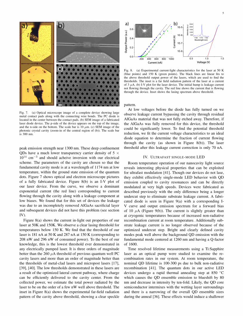
For our structures, we fabricate one large PC lattice withthree uncoupled cavities spaced by six or more lattice periodsin passive GaAs material (Figure 13(a-c)). The number oflinked cavities can be increased further but for the presentdemonstration we use three. The local hole radius and latticeconstant can be tuned so that the cavity modes have identicalor different wavelengths. An example where different wave-lengths are desirable would be for having multiplexed sourcesor modulators for different channels. Identical wavelengthsmight be useful for matching a source with a modulator, asource with a detector, etc. The doping layout is such thatlarge intrinsic regions separate adjacent cavities (Figure 13(c)).This is done so that an applied bias to one set of contacts doesnot produce a crosstalk current flow in a neighboring cavity.Finally, trenches are fabricated to isolate each metal contactpad to eliminate crosstalk (Figure 13(a)).
To couple all three cavities we again use a fiber taperwaveguide that is appropriately placed on all three cavities.When positioned properly, we obtain clear transmission signalsfor each cavity (Figure 13(d)). In this example, the three cavitymodes were fabricated to have unique wavelengths near 1500
8
N N N
P P PI I
a) b)
c) d)
Fig. 13. (a) Tilted SEM picture of a fabricated triple cavity device. Theindependent contact pads are seen along with the isolation trenches. (b) Zoom-in SEM of (a). The doping profile is partially visible. (c) Top-down SEM ofa device with doping regions labeled and delineated by dashed lines. Thescale bar is 2 µm. (d) Transmission spectrum for a fiber taper coupled to aset of three cavities. The fundamental mode was designed to be at a uniquewavelength for each cavity. Independent tuning of each mode is possible.
nm for modulation studies. As a forward bias is applied toa single pair of contact pads, the corresponding cavity modeis seen to shift in accordance to the modulation propertiesdiscussed above. Meanwhile the other two cavity modes areunaffected by the applied bias. This is repeated with theother two cavity modes with the same result. Therefore, in-dependent electrical control without crosstalk can be achievedin a compact platform. Extensions of this design can easilybe made with any number of active components for denseoptoelectronic integration.
VI. DISCUSSION AND OUTLOOK
We have demonstrated a novel platform for the electricalcontrol of active photonic crystal nanocavity devices. In par-ticular, we have achieved efficient electrical injection into 2Dmembranes of GaAs containing quantum dots for laser andLED applications. Our laser operating at 50K has a thresholdof only 181 nA, the lowest of any electrically driven laserever demonstrated. The lasers operate up to 150K beforetransitioning to LEDs due to limited QD gain and high cavityloss.
The principal reason why we do not observe lasing at roomtemperature is that the quality factor of our cavities is too low,and hence the cavity loss is too great compared to the suppliedQD gain. Previous reports on InAs quantum dot lasers showedthat room temperature lasing in this material system is quitechallenging due to the low maximum gain provided by highdensity QDs, quoted as up to 5 cm−1 per layer [15], [54]. Inorder to realize lasing with such low gain media, the cavityloss must be exceptionally small with Q-factors in excess of104. Our devices, on the other hand, have Q factors rangingfrom 1000-2000, limited by several fabrication complexities.
The first is that the doping regions partially overlap withthe cavity mode field, resulting in free carrier absorption. Thisloss is unavoidable since the p and n regions must be closelyspaced in order to ensure proper carrier injection (see SectionII). The second limitation to the Q-factor we believe is dueto some surface roughening of the GaAs membrane caused
by the repeated deposition and etching of the nitride masks.An additional challenge to room temperature lasing is that theInAs QDs are strongly affected by the rapid thermal anneal at850 C. Their emission strength goes down by a factor of ten atroom temperature, likely due to reduced carrier confinement inthe dots (see Section IV). While it may be possible to optimizethe fabrication process to simultaneously increase the Q-factorand maintain the original QD gain, it will not be trivial.
Alternative to the GaAs platform, indium phosphide withembedded quantum wells might prove to be a better materialsystem for achieving room temperature lasing. QWs havesignificantly more gain than do QDs and room temperaturelasing in InP is routinely observed even for low Q cavities[9], [55], [56]. Quantum wells have even been shown tohave increased photoluminescence intensity after rapid thermalannealing [57]. The main challenge with transferring this plat-form to InP is the relatively high transparancy carrier densityneeded for QW inversion (typically around 1018 cm−3 [56]).As mentioned in section II, achieving high carrier densities atthe cavity center is limited by activated doping levels and non-radiative recombination. Implantation in InP should result insimilar activation levels as for GaAs, though the Si (n dopant)would have a higher activation compared to Be (p dopant)[33]. At the same time, non-radiative recombination for InPhas been shown to be over an order of magnitude slower dueto the positioning of surface trap defects within the bandgap[58], [59]. Our preliminary Poisson simulations show that itshould be possible to attain inversion in QWs and lasing atroom temperature in properly designed InP lateral junctions.If this can be done, practical low-threshold lasers with highoutput powers and fast modulation rates could become a truereality for on-chip photonics.
The uniquely modified properties of our quantum dots atroom temperature have allowed us to demonstrate a 10 GHzsingle-mode LED with sub-fJ/bit energy consumption. While atraditional laser is typically the device of choice for an opticalsource, our single-mode LED has all the look and feel of alaser and can be used for practical communications. The cavityallows light to be efficiently channeled into a well-definedmode that can be further extracted with a coupled waveguide.The narrow spectral linewidth also allows for wavelength di-vision multiplexing in densely integrated systems. Low outputpower remains an issue in these types of sources relyingon non-radiative recombination alone. A fast, single-modeLED that is also very efficient by having a large Purcellenhancement would require sophisticated engineering of thematerial system and careful optimization of cavity parameters[60]. We point out, however, that even though our LEDs arelow power, optical interconnect links could be designed aroundsuch transmitters by using sensitive detector technology.
Finally, we have utilized our lateral p-i-n junction to demon-strate LEDs in 1D photonic crystal nanobeams and fiber-coupled modulators and detectors. The former work is an en-couraging result in that electrical injection can be surprisinglyefficient for such small structures. Nanobeams have conductingcross-sectional areas of just a few hundred square nanometers,yet high current densities and carrier injection levels similarto those of 2D membranes are possible.

9
Our electro-optic modulator and two-photon photodetectorpresent alternative functions for the lateral p-i-n structurenot related to light emission. Here we show that a cavitycan be controlled through free carrier dispersion and in theprocess modulate light output through a coupled fiber taper.Cavity-enhanced TPA and photocurrent generation open upanother avenue for electrical PC cavity control. Going forward,integrated components such as the triple cavity for wavelengthdivision multiplexing will be important for full system appli-cations.
In summary, we have developed a technique for bothefficient electrical injection and electrical control of photoniccrystal cavities. Design flexibility is inherent in our platformand numerous parameters can be easily changed to provide acustom need. The extra degree of freedom provided throughelectrical control could lead to new physics and studies on theinteraction between light and matter, as well as in optome-chanics.
ACKNOWLEDGMENT
Gary Shambat and Bryan Ellis were supported by theStanford Graduate Fellowship. Gary Shambat is also supportedby the NSF GRFP. The authors acknowledge the financialsupport of the Interconnect Focus Center, one of the sixresearch centers funded under the Focus Center ResearchProgram, a Semiconductor Research Corporation program. Wealso acknowledge the AFOSR MURI for Complex and RobustOn-chip Nanophotonics (Dr. Gernot Pomrenke), grant numberFA9550-09-1-0704, and the Director, Office of Science, Officeof Basic Energy Sciences, Materials Sciences and EngineeringDivision, of the US Department of Energy under ContractNo. DE-AC02-05CH11231. Work was performed in part atthe Stanford Nanofabrication Facility of NNIN supported bythe National Science Foundation. We also acknowledge KelleyRivoire for assisting in SEM image acquisition.
REFERENCES
[1] J. Vuckovic, M. Loncar, H. Mabuchi, and A. Scherer, “Optimization ofQ-factor in photonic crystal microcavities,” IEEE J. Quantum. Elec., vol.38, pp. 850-856, 2002.
[2] Y. Akahane, T. Asano, B.S. Song, and S. Noda, “High-Q photonicnanocavity in a two-dimensional photonic crystal,” Nature, vol. 425, pp.944-947, 2003.
[3] B.S. Song, S. Noda, T. Asano, and Y. Akahane, “Ultra-high-Q photonicdouble-heterostructure nanocavity,” Nat. Mater., vol. 4, pp. 207-210, 2005.
[4] Y. Tanaka, J. Upham, T. Nagashima, T. Sugiya, T. Asano, and S. Noda,“Dynamic control of the Q factor in a photonic crystal nanocavity,” Nat.Mater., vol. 6, pp. 862-865, 2007.
[5] J. Chan, T. P. M. Alegre, A. H. Safavi-Naeini, J. T. Hill, A. Krausse,S. Groblacher, M. Aspelmeyer, and O. Painter, “Laser cooling of ananomechanical oscillator into its quantum ground state,” Nature, vol.478, pp. 89-92, 2011.
[6] D. Englund, A. Faraon, I. Fushman, N. Stoltz, P. Petroff, and J. Vuckovic,“Controlling cavity reflectivity with a single quantum dot,” Nature, vol.450, pp. 857-861, 2007.
[7] J. S. Foresi, P. R. Villeneuve, J. Ferrera, E. R. Thoen, G. Steinmeyer,S. Fan, J. D. Joannopoulos, L. C. Kimmerling, H. I. Smith, and E. P. Ip-pen, “Photonic-bandgap microcavities in optical waveguides,” Nature, vol.390, pp. 143-145, 1997.
[8] O. Painter, J. Vuckovic, and A. Scherer, “Defect modes of a two-dimensional photonic crystal in an optically thin dielectric slab,” J. Opt.Soc. Am. B, vol. 16, pp. 275-285, 1999.
[9] O. Painter, R. K. Lee, A. Scherer, A. Yariv, J. D. O’Brien, P. D. Dapkus,I. Kim, “Two-dimensional photonic band-gap defect mode laser,” Science,vol. 284, pp. 1819-1821, 1999.
[10] S. Noda, “Photonic crystal lasers - ultimate nanolasers and broad areacoherent lasers,” J. Opt. Soc. Am. B, vol. B 27, pp. B1-B8, 2010.
[11] G. Bjork and Y. Yamamoto, “Analysis of semiconductor microcavitylasers using rate equations,” IEEE J. Quantum Elec., vol. 27, pp. 2386-2396, 1991.
[12] S. Strauf, K. Hennessy, M. T.Rakher, Y. S. Choi, A. Badolato, L.C. An-dreani, E. L. Hu, P. M. Petroff, and D. Bouwmeester, “Self-tuned quantumdot gain in photonic crystal lasers,” Phys. Rev. Lett., vol. 96, pp. 127404,2006.
[13] S. Matsuo, A. Shinya, T. Kakitsuka, K. Nozaki, T. Segawa, T. Sato,Y. Kawaguchi, and M. Notomi, “High-speed ultracompact buried het-erostructure photonic-crystal laser with 13 fJ of energy consumed per bittransmitted,” Nat. Photonics, vol. 4, pp. 648-654, 2010.
[14] H. Altug, D. Englund, and J. Vuckovic, “Ultra-fast photonic crystalnanolasers,” Nat. Physics, vol. 2, pp. 484-488, 2006.
[15] M. Nomura, S. Iwamoto, K. Watanabe, N. Kumagai, Y. Nakata,S. Ishida, and Y. Arakawa, “Room temperature continuous-wave lasing inphotonic crystal nanocavity,” Opt. Express, vol. 14, pp. 6308-6315, 2006.
[16] K. Nozaki, H. Watanabe, and T. Baba, “Photonic crystal nanolaser mono-lithically integrated with passive waveguide for effective light extraction,”Appl. Phys. Lett., vol. 92, pp. 021108, 2008.
[17] H. G. Park, S. H. Kim, S. H. Kwon, Y. G. Ju, J. K. Yang, J. H. Baek,S. B. Kim, and Y. H. Lee, “Electrically driven single-cell photonic crystallaser,” Science, vol. 305, pp. 1444-1447, 2005.
[18] H. G. Park, S. H. Kim, M. K. Seo, Y. G. Ju, S. B. Kim, and Y. H. Lee,“Characteristics of electrically driven two-dimensional photonic crystallaser,” IEEE J. Quantum Elec., vol. 41, pp. 1131-1141, 2005.
[19] M. H. Macdougal, P. D. Dapkus, V. Pudikov, H. Zhao, and G. M. Yang,“Ultralow threshold current vertical-cavity surface-emitting lasers withAlAs oxide-GaAs distributed Bragg reflectors,” IEEE Photon. Technol.Lett., vol. 7, pp. 229-231, 1995.
[20] M. Francardi, L. Balet, A. Gerardino, N. Chauvin, D. Bitauld, L. H. Li,B. Alloing, and A. Fiore, “Enhanced spontaneous emission in a photonic-crystal light-emitting diode,” Appl. Phys. Lett., vol. 93, pp. 143102, 2008.
[21] S. Chakravarty, P. Bhattacharya, J. Topol’ancik, and Z. Wu, “Electricallyinjected quantum dot photonic crystal microcavity light emitters andmicrocavity arrays,” J. Phys. D: Appl. Phys., vol. 40, pp. 2683-2690,2007.
[22] B. Ellis, T. Sarmiento, M. A. Mayer, B. Zhang, J. Harris, E. E. Haller,and J. Vuckovic, “Electrically pumped photonic crystal nanocavity lightsources using a laterally doped p-i-n junction,” Appl. Phys. Lett., vol. 96,pp. 181103, 2010.
[23] B. Ellis, M. A. Mayer, G. Shambat, T. Sarmiento, James S. Harris,E. E. Haller, and J. Vuckovic, “Ultralow-threshold electrically pumpedquantum dot photonic-crystal nanocavity laser,” Nat. Photonics, vol. 5,pp. 297-300, 2011.
[24] I. W. Frank, P. B. Deotare, M. W. McCutcheon, and M. Loncar,“Programmable photonic crystal nanobeam cavities,” Opt. Express, vol.18, pp. 8705-8712, 2010.
[25] A. Faraon, A. Majumdar, H. Kim, P. Petroff, and J. Vuckovic, “Fastelectrical control of a quantum dot strongly coupled to a photonic crystalcavity,” Phys. Rev. Lett., vol. 104, pp. 047402, 2010.
[26] Q. Xu, B. Schmidt, S. Pradhan, and M. Lipson, “Micrometre-scalesilicon electro-optic modulator,” Nature, vol. 435, pp. 325-327, 2005.
[27] T. Tanabe, K. Nishiguchi, E. Kuramochi, and M. Notomi, “Low powerand fast electro-optic silicon modulator with lateral p-i-n embeddedphotonic crystal nanocavity,” Opt. Express, vol. 17, pp. 22505-22503,2009.
[28] T. Tanabe, H. Sumikura, H. Taniyama, A. Shinya, and M. Notomi, “All-silicon sub-Gb/s telecom detector with low dark current and high quantumefficiency on chip,” Appl. Phys. Lett., vol. 96, pp. 101103, 2010.
[29] H. Watanabe and T. Baba, “Active/passive-integrated photonic crystalslab micro-laser,” Elec. Lett., vol. 42, pp. 695-696, 2006.
[30] A. Tager, R. Gaska, I. Avrutzky, M. Fay, H. Chik, A. SpringThorpe,S. Eicher, J. M. Xu, and M. Shur, “Ion-implanted GaAs-InGaAs lateralcurrent injection laser,” IEEE J. Sel. Top. Quant., vol. 5, pp. 664-672,1999.
[31] C. M. Long, A. V. Giannopoulos, and K. D. Choquette, “Modifiedspontaneous emission from laterally injected photonic crystal emitter,”Elec. Lett., vol. 45, pp. 227-228, 2009.
[32] D. Englund, H. Altug, and J. Vuckovic, “Low-threshold surface-passivated photonic crystal nanocavity laser,” Appl. Phys. Lett., vol. 91,071124, 2007.

10
[33] M. V. Rao, “Ion implantation in III-V compound semiconductors,” Nucl.Instrum. Meth. B., vol. 79, 645-647, 1993.
[34] C. C. Williams, “Two-dimensional dopant profiling by scanning capac-itance microscopy,” Ann. Rev. Mater. Sci., vol. 29, 471-504, 1999.
[35] G. Shambat, B. Ellis, M. A. Mayer, J. Petykiewicz, T. Sarmiento,James S. Harris, E. E. Haller, and J. Vuckovic, “Nanobeam photoniccrystal cavity light-emitting diodes,” Appl. Phys. Lett., vol. 99, 071105,2011.
[36] S. Malik, C. Roberts, R. Murray, and M. Pate, “Tuning self-assembledInAs quantum dots by rapid thermal annealing,” Appl. Phys. Lett., vol.71, 1987-1989, 1997.
[37] Y. H. Lee, B. Tell, K. Brown-Goebeler, J. L. Jewell, and J. V. Hove,“Top-surface-emitting GaAs four-quantum-well lasers emitting at 0.85µm,” Elec. Lett., vol. 26, 710-711, 1990.
[38] A. Berrier, M. Mulot, G. Malm, M. Ostling, and S. Anand, “Carriertransport through a dry-etched InP-based two-dimensional photonic crys-tal,” J. Appl. Phys., vol. 101, 123101, 2007.
[39] M. T. Hill, Y. S. Oei, B. Smalbrugge, Y. Zhu, T. de Vries, P. J. van Veld-hoven, F. W. M. van Otten, T. J. Eijkemans, J. P. Turkiewicz,H. de Waardt, E. J. Geluk, S. H. Kwon, Y. H. Lee, R. Notzel, andM. K. Smith, “Lasing in metallic-coated nanocavities,” Nat. Photonics,vol. 1, pp. 589-594, 2007.
[40] S. Reitzenstein, T. Heindel, C. Kistner, A. Rahimi-Iman, C. Schneider,S. Hofling, and A. Forchel, “Low threshold electrically pumped quantumdot-micropillar lasers,” Appl. Phys. Lett., vol. 93, 061104, 2008.
[41] G. Shambat, B. Ellis, A. Majumdar, J. Petykiewicz, M. A. Mayer,T. Sarmiento, James S. Harris, E. E. Haller, and J. Vuckovic, “Ultrafastdirect modulation of a single-mode photonic crystal nanocavity light-emitting diode,” Nat. Comm., vol. 2, 539, 2011.
[42] S. Assefa, F. Xia, and Y. A. Vlasov, “Reinventing germanium avalanchephotodetector for nanophotonic on-chip optical interconnects,” Nature,vol. 464, 80-85, 2010.
[43] O. Hayden, R. Agarwal, and C. M. Lieber, “Nanoscale avalanchephotodiodes for highly sensitive and spatially resolved photon detection,”Nat. Mater., vol. 5, 352-356, 2006.
[44] Y. Gong and J. Vuckovic, “Photonic crystal cavities in silicon dioxide,”Appl. Phys. Lett., vol. 96, 031107, 2010.
[45] Y. Gong, M. Makarova, S. Yerci, R. Li, M. J. Steven, B. Baek,S. W. Nam, L. Dal Negro, and J. Vuckovic, “Observation of transparencyof erbium-doped silicon nitride in photonic crystal nanobeam cavities,”Opt. Express, vol. 18, 12176-12184, 2010.
[46] Y. Zhang, M. Khan, Y. Huang, J. H. Ryou, P. B. Deotare, R. Dupuis,and M. Loncar, “Photonic crystal nanobeam lasers,” Appl. Phys. Lett.,vol. 97, 051104, 2010.
[47] M. Eichenfield, J. Chan, R. Camacho, K. J. Vahala, and O. Painter,“Optomechanical crystals,” Nature, vol. 462, 78-82, 2009.
[48] B. Wang, M. A. Dundar, R. Notzel, F. Karouta, S. He, andR. W. van der Heijden, “Photonic crystal slot nanobeam slow lightwaveguides for refractive index sensing,” Appl. Phys. Lett., vol. 97,151105, 2010.
[49] G. Shambat, B. Ellis, M. A. Mayer, A. Majumdar, E. E. Haller, andJ. Vuckovic, “Ultra-low power fiber-coupled gallium arsenide photoniccrystal cavity electro-optic modulator,” Opt. Express, vol. 19, 7530-7536,2011.
[50] G. Shambat, Y. Gong, J. Lu, S. Yerci, R. Li, L. Dal Negro, andJ. Vuckovic, “Coupled fiber taper extraction of 1.53 µm photolumines-cence from erbium doped silicon nitride photonic crystal cavities,” Opt.Express, vol. 18, 5964-5973, 2010.
[51] K. Kishino, M. S. Unlu, J. I. Chyi, J. Reed, L. Arsenault, and H. Morkoc,“Resonant cavity-enhanced (RCE) photodetectors,” IEEE J. QuantumElec., vol. 27, 2025-2034, 1991.
[52] K. Nozaki, T. Tanabe, A. Shinya, S. Matsuo, T. Sato, H. Taniyama,and M. Notomi, “Sub-femtojoule all-optical switching using a photonic-crystal nanocavity,” Nat. Photonics, vol. 4, 477-483, 2010.
[53] S. Manipatruni, L. Chen, and M. Lipson, “Ultra high bandwidth WDMusing silicon microring modulators,” Opt. Express, vol. 18, 16858-16867,2010.
[54] K. Srinivasan, M. Borselli, T. J. Johnson, P. E. Barclay, and O. Painter,“Optical loss and lasing characteristics of high-quality-factor AlGaAsmicrodisk resonators with embedded quantum dots,” Appl. Phys. Lett.,vol. 86, 151106, 2005.
[55] M. Loncar, T. Yoshie, A. Schere, P. Gogna, and Y. Qiu, “Low thresholdphotonic crystal laser,” Appl. Phys. Lett., vol. 81, pp. 2680, 2002.
[56] H. Altug and J. Vuckovic, “Photonic crystal nanocavity array laser,” Opt.Express, vol. 13, 8819-8828, 2005.
[57] C. Y. Lee, M. C. Wu, Y. D. Tian, W. H. Wang, W. J. Ho, and T. T. Shi,“Effects of rapid thermal annealing on InAsP/InP strained multiquantumwell laser diodes grown by metal organic chemical vapour deposition,”Elec. Lett., vol. 36, 1026-1028, 2000.
[58] D. D. Nolte, “Surface recombination, free-carrier saturation, and dan-gling bonds in InP and GaAs,” Solid State Electron., vol. 33, 295-298,1990.
[59] J. F. Holzman, P. Strasser, R. Wuest, F. Robin, D. Erni, and H. Jackel,“Ultrafast carrier dynamics in InP photonic crystals,” Nanotechnology,vol. 16, 949-952, 2005.
[60] E. K. Lau, A. Lakhani, R. S. Tucker, and M. C. Wu, “Enhanced modu-lation bandwidth of nanocavity light emitting devices,” Opt. Express, vol.17, 7790-7999, 2009.
Related Documents