Electrical Properties and Interfacial Characteristics of RuO 2 Õ HfAlO x Õ SiON Õ Si and RuO 2 Õ LaAlO 3 Õ SiON Õ Si Capacitors V. Edon, a,f,z Z. Li, a M.-C. Hugon, a C. Krug, b K. P. Bastos, b L. Miotti, b I. J. R. Baumvol, c C. Cardinaud, c O. Durand, d,g and C. Eypert e a Laboratoire de Physique des Gaz et des Plasmas, Université Paris-Sud, UMR8578, F-91405 Orsay, France b Universidade de Caxias do Sul, CCET, 95070-580, Caxias do Sul, Brazil and Instituto de Física, UFRGS, Porto Alegre, Brazil c Laboratoire des Plasmas et des Couches Minces, Institut des Matériaux Jean Rouxel, Université de Nantes, UMR 6502, F-44322, Nantes, France d Laboratoire d’Analyses Physiques Avancées, Thales Research & Technology, F-91767 Palaiseau, France e Thin Film Division, HORIBA Jobin Yvon S.A.S., F-91380 Chilly-Mazarin, France Electrical and structural properties of metal-oxide-semiconductor capacitors having as dielectric nanoscopic LaAlO 3 or HfAlO x films deposited on nitrided or nonnitrided Si substrates were investigated. The electrical superiority of RuO 2 /HfAlO x /SiON/Si stacks was evidenced by a dielectric constant of 19 and a leakage current density of 67 mA/cm 2 at a gate voltage of -1 V, for a capacitance equivalent to silicon oxide thickness of 1.1 nm. Morphology, composition, and structure of the stacks were accessed by X-ray diffraction and reflectometry, spectroscopic ellipsometry, X-ray photoelectron spectroscopy, and narrow resonant nuclear reaction profiling with isotopic substitution. In spite of presenting crystalline phases associated with HfO 2 , the HfAlO x dielectric layers led to a smoother and thinner interfacial layer, improved by the thermal nitridation of the Si substrate prior to high- deposition. This SiON-like interlayer thickness is self-limited even after postdeposition annealing owing to the formation of an effective diffusion barrier by the strong N–Si–N and N–Si–O–N bonds, which is also effective in preventing substrate oxidation. © 2008 The Electrochemical Society. DOI: 10.1149/1.2952529 All rights reserved. Manuscript submitted February 29, 2008; revised manuscript received June 2, 2008. Published July 15, 2008. Hafnium-based high- gate dielectrics are incorporated 1 into Si- based metal-oxide-semiconductor field-effect transistor MOSFET fabrication technology. The first commercial advanced processors have been available for a few months, the gate dielectric consisting most probably of amorphous HfSiON compound ultrathin films, 2 which have the required combination of electrical characteristics as required by design rules, as well as integrity and structural and chemical stability. However, the magnitude of the reported 3 dielec- tric constants for these films indicate that they are only sufficient for this and, eventually, the next generation of ultra-large-scale inte- grated devices; whereas for forthcoming device generations, an al- ternative, higher dielectric constant material will have to be used. In particular, several potential candidates, such as binary and ternary oxides, have been investigated. Among them, lanthanum and hafnium aluminates LaAlO 3 and HfAlO x , respectively have been considered in view of their good thermal stability on Si. 4-9 Other relevant properties for device purposes, such as dielectric constant, crystallization temperature, optical bandgap, valence, and conduc- tion band offsets, depend on the Al /La or Al /Hf ratios in these thin-film compositions. 10,11 In particular, in order to guarantee an amorphous structure and a satisfactory thermal stability on Si of HfAlO x thin films, it has been reported 12 that nearly 30% of Al 2 O 3 is required. Studies 7,13 have also pointed out the effect on film prop- erties of the interfacial layer formed between dielectric material and substrate. Intermixing between oxide and Si has been reported, 5 fol- lowing deposition or postdeposition annealing. This interlayer is usually composed of a La or Hf–Al–O–Si compound, which often decreases the dielectric constant of the metal-oxide-semiconductor MOS capacitors as well as the capacitance equivalent to silicon oxide thickness EOT. 14 A convenient solution 15 is provided by thermal nitridation of the substrate in ammonia NH 3 , a self-limited thermal growth process that forms a few monolayers of silicon ox- ynitride SiON on Si before high- deposition. This subnanometric interfacial layer inhibits atomic transport and chemical reaction, re- ducing the above-mentioned deleterious effects. This paper reports on a comparative investigation of electrical characteristics of LaAlO 3 and HfAlO x dielectric materials deposited on Si or on thermally grown SiON/Si, correlated with composition and structural properties as established by several different analyti- cal methods such as X-ray diffraction XRD and X-ray reflectom- etry XRR, far UV spectroscopic ellipsometry, X-ray photoelectron spectroscopy XPS, isotopic substitution, and narrow resonant nuclear reaction profiling. Experimental Lanthanum and hafnium aluminates were deposited by radio-frequency magnetron sputtering, from LaAlO 3 and HfO 2 0.3 Al 2 O 3 0.7 ceramic targets. Power density and gas pressure were fixed at 1 W/cm 2 and 5 Pa, respectively. Si 001 substrates were chemically cleaned followed by HF-last. The composition of the films was determined by Rutherford backscattering spectrometry and nuclear reaction analysis. Some of the Si substrates were ther- mally nitrided at 700°C for 30 s in 10 mbar of NH 3 , or in 10 mbar of NH 3 isotopically enriched in the 15 N isotope 15 NH 3 . This is a self-limited growth process 16,17 that leads to the formation of an 0.4 nm thick SiON film, resistant to the critical dopant activation thermal processing step of fabrication technology, usually performed at 1000°C for 10 s. In order to produce MOS structures, a RuO 2 electrode was deposited by reactive magnetron sputtering from a Ru target in Ar /O 2 plasma. Samples were analyzed before and after postdeposition annealing PDA in O 2 at 600°C for 30 min. Capacitance-voltage C-V at 1 MHz and current-voltage I-V char- acteristics were determined for 3 10 -3 cm 2 capacitors. Morphol- ogy of thicker films 60–120 nm deposited in identical conditions was investigated by XRD analysis, using an Inel CPS-120 curved detector, equipped with a Ge 220-crystal incident-beam monochro- mator. The incident beam angle was kept at 8° with respect to the sample surface. XRR was performed using a Bruker-AXS D8- Discover goniometer working with Cu K radiation selected by means of a graphite scattered-beam monochromator. Fast Fourier transform of the XRR curves 18 led to the absolute determination of the individual layer thicknesses, whereas numeric simulation has been used for estimation of interfacial roughness. Far UV spectro- scopic ellipsometry FUV-SE measurements were performed using a UVISEL device from HORIBA Jobin Yvon. The composition of the stacks was determined in the spectral range of 190–850 nm, f Present address: IEMN, Antenne USTL, F-59655 Villeneuve d’Ascq, France. g Present address: LENS/FOTON, INSA, 20 av. des Buttes de Coësmes F-35043 Rennes. z E-mail: [email protected] Journal of The Electrochemical Society, 155 9 H661-H668 2008 0013-4651/2008/1559/H661/8/$23.00 © The Electrochemical Society H661 Downloaded 21 Jul 2008 to 134.206.35.217. Redistribution subject to ECS license or copyright; see http://www.ecsdl.org/terms_use.jsp

Welcome message from author
This document is posted to help you gain knowledge. Please leave a comment to let me know what you think about it! Share it to your friends and learn new things together.
Transcript

Journal of The Electrochemical Society, 155 �9� H661-H668 �2008� H661
Electrical Properties and Interfacial Characteristics ofRuO2ÕHfAlOxÕSiONÕSi and RuO2ÕLaAlO3ÕSiONÕSi CapacitorsV. Edon,a,f,z Z. Li,a M.-C. Hugon,a C. Krug,b K. P. Bastos,b L. Miotti,b
I. J. R. Baumvol,c C. Cardinaud,c O. Durand,d,g and C. Eyperte
aLaboratoire de Physique des Gaz et des Plasmas, Université Paris-Sud, UMR8578, F-91405 Orsay,FrancebUniversidade de Caxias do Sul, CCET, 95070-580, Caxias do Sul, Brazil and Instituto de Física, UFRGS,Porto Alegre, BrazilcLaboratoire des Plasmas et des Couches Minces, Institut des Matériaux Jean Rouxel, Université deNantes, UMR 6502, F-44322, Nantes, FrancedLaboratoire d’Analyses Physiques Avancées, Thales Research & Technology, F-91767 Palaiseau, FranceeThin Film Division, HORIBA Jobin Yvon S.A.S., F-91380 Chilly-Mazarin, France
Electrical and structural properties of metal-oxide-semiconductor capacitors having as dielectric nanoscopic LaAlO3 or HfAlOxfilms deposited on nitrided or nonnitrided Si substrates were investigated. The electrical superiority of RuO2/HfAlOx/SiON/Sistacks was evidenced by a dielectric constant of 19 and a leakage current density of 67 mA/cm2 at a gate voltage of −1 V, for acapacitance equivalent to silicon oxide thickness of 1.1 nm. Morphology, composition, and structure of the stacks were accessedby X-ray diffraction and reflectometry, spectroscopic ellipsometry, X-ray photoelectron spectroscopy, and narrow resonant nuclearreaction profiling with isotopic substitution. In spite of presenting crystalline phases associated with HfO2, the HfAlOx dielectriclayers led to a smoother and thinner interfacial layer, improved by the thermal nitridation of the Si substrate prior to high-�deposition. This SiON-like interlayer thickness is self-limited even after postdeposition annealing owing to the formation of aneffective diffusion barrier by the strong N–Si–N and N–Si–O–N bonds, which is also effective in preventing substrate oxidation.© 2008 The Electrochemical Society. �DOI: 10.1149/1.2952529� All rights reserved.
Manuscript submitted February 29, 2008; revised manuscript received June 2, 2008. Published July 15, 2008.
0013-4651/2008/155�9�/H661/8/$23.00 © The Electrochemical Society
Hafnium-based high-� gate dielectrics are incorporated1 into Si-based metal-oxide-semiconductor field-effect transistor �MOSFET�fabrication technology. The first commercial advanced processorshave been available for a few months, the gate dielectric consistingmost probably of amorphous HfSiON compound ultrathin films,2
which have the required combination of electrical characteristics asrequired by design rules, as well as integrity and structural andchemical stability. However, the magnitude of the reported3 dielec-tric constants for these films indicate that they are only sufficient forthis and, eventually, the next generation of ultra-large-scale inte-grated devices; whereas for forthcoming device generations, an al-ternative, higher dielectric constant material will have to be used. Inparticular, several potential candidates, such as binary and ternaryoxides, have been investigated. Among them, lanthanum andhafnium aluminates �LaAlO3 and HfAlOx, respectively� have beenconsidered in view of their good thermal stability on Si.4-9 Otherrelevant properties for device purposes, such as dielectric constant,crystallization temperature, optical bandgap, valence, and conduc-tion band offsets, depend on the Al/La or Al/Hf ratios in thesethin-film compositions.10,11 In particular, in order to guarantee anamorphous structure and a satisfactory thermal stability on Si ofHfAlOx thin films, it has been reported12 that nearly 30% of Al2O3is required. Studies7,13 have also pointed out the effect on film prop-erties of the interfacial layer formed between dielectric material andsubstrate. Intermixing between oxide and Si has been reported,5 fol-lowing deposition or postdeposition annealing. This interlayer isusually composed of a La�or Hf�–Al–O–Si compound, which oftendecreases the dielectric constant of the metal-oxide-semiconductor�MOS� capacitors as well as the capacitance equivalent to siliconoxide thickness �EOT�.14 A convenient solution15 is provided bythermal nitridation of the substrate in ammonia �NH3�, a self-limitedthermal growth process that forms a few monolayers of silicon ox-ynitride �SiON� on Si before high-� deposition. This subnanometricinterfacial layer inhibits atomic transport and chemical reaction, re-ducing the above-mentioned deleterious effects.
f Present address: IEMN, Antenne USTL, F-59655 Villeneuve d’Ascq, France.g Present address: LENS/FOTON, INSA, 20 av. des Buttes de Coësmes F-35043
Rennes.z E-mail: [email protected]
Downloaded 21 Jul 2008 to 134.206.35.217. Redistribution subject to E
This paper reports on a comparative investigation of electricalcharacteristics of LaAlO3 and HfAlOx dielectric materials depositedon Si or on thermally grown SiON/Si, correlated with compositionand structural properties as established by several different analyti-cal methods such as X-ray diffraction �XRD� and X-ray reflectom-etry �XRR�, far UV spectroscopic ellipsometry, X-ray photoelectronspectroscopy �XPS�, isotopic substitution, and narrow resonantnuclear reaction profiling.
Experimental
Lanthanum and hafnium aluminates were deposited byradio-frequency magnetron sputtering, from LaAlO3 and�HfO2�0.3�Al2O3�0.7 ceramic targets. Power density and gas pressurewere fixed at 1 W/cm2 and 5 Pa, respectively. Si�001� substrateswere chemically cleaned followed by HF-last. The composition ofthe films was determined by Rutherford backscattering spectrometryand nuclear reaction analysis. Some of the Si substrates were ther-mally nitrided at 700°C for 30 s in 10 mbar of NH3, or in 10 mbarof NH3 isotopically enriched in the 15N isotope � 15NH3�. This is aself-limited growth process16,17 that leads to the formation of an�0.4 nm thick SiON film, resistant to the critical dopant activationthermal processing step of fabrication technology, usually performedat 1000°C for 10 s. In order to produce MOS structures, a RuO2electrode was deposited by reactive magnetron sputtering from a Rutarget in Ar/O2 plasma. Samples were analyzed before and afterpostdeposition annealing �PDA� in O2 at 600°C for 30 min.Capacitance-voltage �C-V� at 1 MHz and current-voltage �I-V� char-acteristics were determined for 3 � 10−3 cm2 capacitors. Morphol-ogy of thicker films �60–120 nm� deposited in identical conditionswas investigated by XRD analysis, using an Inel CPS-120 curveddetector, equipped with a Ge �220�-crystal incident-beam monochro-mator. The incident beam angle was kept at 8° with respect to thesample surface. XRR was performed using a Bruker-AXS D8-Discover goniometer working with Cu K� radiation selected bymeans of a graphite scattered-beam monochromator. Fast Fouriertransform of the XRR curves18 led to the absolute determination ofthe individual layer thicknesses, whereas numeric simulation hasbeen used for estimation of interfacial roughness. Far UV spectro-scopic ellipsometry �FUV-SE� measurements were performed usinga UVISEL device from HORIBA Jobin Yvon. The composition ofthe stacks was determined in the spectral range of 190–850 nm,
CS license or copyright; see http://www.ecsdl.org/terms_use.jsp

H662 Journal of The Electrochemical Society, 155 �9� H661-H668 �2008�H662
using the thicknesses extracted from XRR analysis as inputs. XPSwas performed on a Kratos Axis-Ultra spectrometer using the Al K�line �h� = 1486.6 eV�. For the LaAlO3 films, the Si 2s core levelwas chosen because the Si 2p overlaps with the La 4f. Nitrogen andoxygen profiles were determined with subnanometric depth reso-lution by narrow resonant nuclear reaction profiling �NRP�,19,20 us-ing the 15N�p,���12C and 18O�p,���15N nuclear reactions.
Results and Discussion
Electrical properties of films deposited on Si.— Figure 1 showsthe C-V characteristics for capacitors made with 4 nm LaAlO3 �Fig.1a� and HfAlOx �Fig. 1b� films before and after annealing in O2 at600°C. In both cases, PDA strongly reduces the flatband voltageshift and hysteresis, these effects being more pronounced forRuO2/HfAlOx/Si MOS structures. Similar effects have been ob-served on thicker films �not shown here�. The corresponding EOT vsfilm thicknesses as determined from the C-V characteristics afterPDA are given on the insets. Calculated dielectric constants arefound to be 13 and 12, respectively, whereas EOT are close to2.5 nm for 4 nm thick films. RuO2/LaAlO3/Si samples have a �value slightly larger than that of RuO2/HfAlOx/Si owing to thelarger capacitance in accumulation regime. However, these � valuesare far from the targeted values, namely, those close to the bulkdielectric constants �25 for LaAlO3 and 20 for HfAlOx�. The muchlower � values have been attributed21 to the lower density of theoxide amorphous phases, as compared to the crystalline one. The
Figure 1. C-V characteristics at 1 MHz for �a� RuO2/LaAlO3�4 nm�/Si and�b� RuO2/HfAlOx�4 nm�/Si capacitors, as-deposited or annealed in O2 at600°C. Theoretical curves are obtained assuming a work function of 5 eVfor RuO2. In the insets are given the corresponding EOT � film thicknesses.
Downloaded 21 Jul 2008 to 134.206.35.217. Redistribution subject to E
capacitance equivalent interface thicknesses �EIT� are determined as1.3 and 1.1 nm for RuO2/LaAlO3/Si and RuO2/HfAlOx/Si, respec-tively, which can be associated to the formation of interfacial layersduring film deposition or PDA.9
In order to obtain the electrical characteristics quoted in the pre-vious paragraph, we used a reconstruction model to extract the in-trinsic capacitance from the measured nonideal C-V data owing tothe presence of an interlayer with lower dielectric constant than thehigh-� LaAlO3 and HfAlOx films. It was found22 that an interlayerof different �lower, in particular� dielectric constant causes a fre-quency dispersion of the C-V data. After correction using the modelformula, one can recover the actual C-V plots, free from any fre-quency dispersion effect and give the actual capacitance figures atall frequencies. Thus, by applying this correction, we could avoidany effect of series association of capacitors due to the differentcapacitances of the dielectric layers. The details of the used recon-struction model are far beyond the scope of the present work but canbe found in Ref. 22.
I-V characteristics are given in Fig. 2, for capacitors made with4 nm LaAlO3 �Fig. 2a� and HfAlOx �Fig. 2b� films deposited on Si,before and after PDA. RuO2/LaAlO3/Si structures show a decreaseof three decades for gate current density measured at −1 V afterPDA, whereas the current density obtained from RuO2/HfAlOx/Sicapacitors is two orders of magnitude higher after PDA in the sameconditions. In the case of LaAlO3, the decrease may be a result of alower density of defects in the dielectric layer and/or in thedielectric/Si interface, in agreement with previous observationsmade from C-V characteristics.23 For RuO /HfAlO /Si capacitor
Figure 2. I-V characteristics for �a� RuO2/LaAlO3�4 nm�/Si and �b�RuO2/HfAlOx�4 nm�/Si capacitors, as-deposited or annealed in O2 at 600°C.
2 x
CS license or copyright; see http://www.ecsdl.org/terms_use.jsp

H663Journal of The Electrochemical Society, 155 �9� H661-H668 �2008� H663
samples, the increase on leakage current density observed after an-nealing seems inconsistent with the smaller amount of charge trapsin the dielectric or in the oxide/Si interface, observed on C-V mea-surements. In this case, the reason for the observed increase in cur-rent density must be some other characteristic of the dielectric,whose investigation will be described below.
XRD analysis of films deposited on Si.— XRD analysis was un-dertaken in order to elucidate the discrepancies in gate current den-sities after PDA of capacitors made with the two different materialsas described at the end of the previous paragraph. Diffractogramsare shown in Fig. 3, for 60 nm LaAlO3 �Fig. 3a� and 120 nmHfAlOx �Fig. 3b� films as-deposited or submitted to PDA in O2 at600°C. LaAlO3 samples remain amorphous even after annealing, inagreement with previous studies,4,5 showing that LaAlO3 crystal-lizes above 800°C. The considerably low leakage currents obtainedfrom RuO2/LaAlO3/Si structures seem to be due to the absence ofgrain boundaries in the amorphous dielectric layer. Both as-deposited and annealed HfAlOx samples show tetragonal-monoclinic phase for 2� near 60–62°, associated with HfO2.24 In-deed, HfO2 films are well known for having a low crystallizationtemperature.25 Consequently, the easy electronic transport throughgrain boundaries can explain the large gate current density observedhere on I-V characteristics of RuO2/HfAlOx/Si structures.
Electrical properties of films deposited on Si or SiON.— Figure4 shows C-V characteristics for capacitors made with nitrided sub-
Figure 3. XRD spectra for �a� LaAlO3/Si and �b� HfAlOx/Si samples, as-deposited or annealed in O2 at 600°C.
Downloaded 21 Jul 2008 to 134.206.35.217. Redistribution subject to E
strates and their non-nitrided counterparts, where 4 nm LaAlO3�Fig. 4a� and HfAlOx �Fig. 4b� dielectric layers have been depositedand submitted to PDA in O2 at 600°C. Concerning fixed chargeslocated in the dielectric film layer, substrate nitridation does notimply degradation of electrical quality of thin films, because theflatband voltage shifts are almost the same as for the non-nitridedsubstrates. However, for RuO2/LaAlO3/SiON/Si structures, theelectronic interface state density �Dit� is larger than for its hafnium-based counterpart �6 � 1013 vs 4.5 � 1011 eV−1 cm−2�. For the lat-ter, the experimental data fall very close to the theoretical curve,where Dit is equal to 8.7 � 1011 eV−1 cm−2, and in agreement withpreviously reported values.26
Corresponding EOT � thicknesses for both dielectric materialsare given in Fig. 5. The characteristics of RuO2/LaAlO3/SiON/Siand RuO2/HfAlOx/SiON/Si capacitors are distinctly superior, be-cause the values of the dielectric constants are 25 and 19, respec-tively, essentially reaching the bulk material figures. A significantdecrease of EOT is also noted, the obtained figures being 1.2 and1.1 nm for 4 nm LaAlO3 and HfAlOx dielectric layers, respectively.EIT are estimated as 0.5 and 0.4 nm, namely equivalent to the initialnitrided interlayer thicknesses before annealing in O2, thus confirm-ing the inertness and antidiffusion capability of the SiON interlayer.
Figure 4. C-V characteristics at 1 MHz for �a� RuO2/LaAlO3�4 nm�/Si andRuO2/LaAlO3�4 nm�/SiON/Si capacitors, and �b� RuO2/HfAlOx�4 nm�/Siand RuO2/HfAlOx�4 nm�/SiON/Si ones, annealed in O2 at 600°C. Theoret-ical curves are obtained assuming a work function of 5 eV for RuO2.
CS license or copyright; see http://www.ecsdl.org/terms_use.jsp

H664 Journal of The Electrochemical Society, 155 �9� H661-H668 �2008�H664
Leakage current densities measured in accumulation at −1 V as afunction of EOT after PDA, for nitrided and non-nitrided substratesare given in Fig. 6a �LaAlO3� and 6b �HfAlOx�. The I-V measure-ments were looped many times from −1 to −6 V and no hysteresiswas observed. In the case of RuO2/LaAlO3/SiON/Si structures, ni-tridation has a dramatic effect on gate current density. It increasesexponentially with the decrease of EOT, becoming up to six ordersof magnitude higher than for non-nitrided structures in the lowerEOT range. For RuO2/HfAlOx/SiON/Si capacitors, although thegate current density also increases exponentially with the decreaseof EOT for capacitors made with non-nitrided substrates, for thosemade with nitrided substrates the current density remains approxi-mately constant with decreasing thickness in the lower EOT range.The measured value of 67 mA/cm2 at −1 V for a 1.1 nm EOT inRuO2/HfAlOx/SiON/Si is comparable to the best results found inthe literature.
The degradation in leakage current observed for RuO2/LaAlO3/SiON/Si capacitors is somehow difficult to understand. Inprinciple, because the dielectric film remains amorphous, the expla-nation should be an increase of electrically active defects locatedeither in the dielectric layer or in the dielectric/SiON/Si interface.Both would be consistent with the determined C-V characteristics.For the RuO2/HfAlOx/SiON/Si, the SiON interlayer seems to havean outstanding effect on stopping electronic migration through thecapacitor dielectric, which satisfactorily compensates the deleteriouseffect of crystallization.
Figure 5. EOT vs film thicknesses after annealing in O2 at 600°C, extractedfrom C-V characteristics for �a� RuO2/LaAlO3/Si and RuO2/LaAlO3/SiON/Si capacitors and �b� RuO2/HfAlOx/Si and RuO2/HfAlOx/SiON/Si.
Downloaded 21 Jul 2008 to 134.206.35.217. Redistribution subject to E
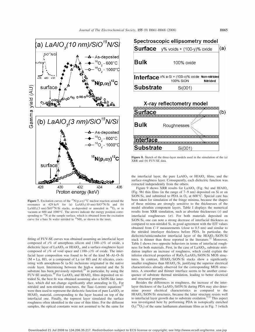
Interfacial structure of films deposited on Si or SiON.— Anotherpossible factor determining the different behaviors of leakage cur-rent after PDA is the stability of the nitrided dielectric/silicon inter-faces. In the case of hafnium aluminates, this has been addressedbefore,9 showing that N incorporated in the near-interface region isnot lost even after 1000°C annealing in O2. The case of theLaAlO3/SiON/Si structures was investigated here by performing ni-tridation in 15NH3 and determining the 15N profiles by narrow reso-nant nuclear reaction profiling using the 15N�p,���12C nuclear re-action. The excitation curves of this reaction near the resonance at429 keV ��R = 120 eV� for LaAlO3�10 nm�/SiO15N/Si andLaAlO3�3 nm�/SiO15N/Si are shown in Fig. 7. One notes the 15Npeak concentrations at the interfaces of the as-deposited samples andthe appreciable loss of 15N after PDA at 600°C, especially from theLaAlO3�3 nm�/SiO15N/Si structures. Thus, the N loss account fromthe interface, which is more pronounced for the thinner films, mayindeed be another possible explanation for the degradation in leak-age current of La-based dielectrics. For completeness, Fig. 7 alsoshows the excitation curves after PDA at 1000°C, 10 s. Althoughthe visibly more pronounced loss of 15N from the near-interfaceregion, there is still 15N remaining in this region, which can accountfor the improvement on MOSFET device electrical characteristics.
A three-layer model depicted in Fig. 8 was adopted for the inter-pretation of XRR results �Fig. 8a� and for FUV-SE results �Fig.8b�.27,28 The interpretation of XRR results takes into account theinterfacial roughness as well as the absolute thickness and density ofthe films. For LaAlO and HfAlO films deposited on Si, the best
Figure 6. Gate current density measured at a voltage of −1 V in accumula-tion vs EOT after annealing in O2 at 600°C for �a� RuO2/LaAlO3/Si andRuO2/LaAlO3/SiON/Si capacitors, and �b� RuO2/HfAlOx/Si andRuO2/HfAlOx/SiON/Si.
3 x
CS license or copyright; see http://www.ecsdl.org/terms_use.jsp
H665Journal of The Electrochemical Society, 155 �9� H661-H668 �2008� H665
fitting of FUV-SE curves was obtained assuming an interfacial layercomposed of x% of amorphous silicon and �100–x�% of oxide, adielectric layer of LaAlO3 or HfAlOx, and a surface-roughness layercomposed of y% of void space and �100–y�% of oxide. The inter-facial layer composition was found to be of the kind M–Al–O–Si�M = La, Hf�, or a compound of La �or Hf� and Al silicates, coex-isting with amorphous-Si �a-Si� inclusions originated in the nativeoxide layer. Intermixing between the high-� material and the Sisubstrate has been previously reported,29 in particular, by using theFUV-SE analysis.30 For LaAlO3 and HfAlOx films deposited on ni-trided Si, the best fit was obtained assuming also a SiON-like inter-face, which did not change significantly after annealing in O2. Fornitrided and non-nitrided structures, the Tauc–Lorentz equations31
were then used to represent the dielectric function of pure LaAlO3 orHfAlOx material, corresponding to the layer located on top of theinterfacial one. Finally, the topmost layer simulated the surfaceroughness often identified in the case of thin films. For the differentsamples, the optical constants were not assumed to be the same for
Figure 7. Excitation curves of the 15N�p,���12C nuclear reaction around theresonance at 429 keV for �a� LaAlO3�10 nm�/SiO15N/Si and �b�LaAlO3�3 nm�/SiO15N/Si stacks, as-deposited or annealed in 18O2 or invacuum at 600 and 1000°C. The arrows indicate the energy position corre-sponding to 15N at the sample surface, which is obtained from the excitationcurve for a bare Si wafer nitrided in 15NH3 as shown in the inset.
Downloaded 21 Jul 2008 to 134.206.35.217. Redistribution subject to E
the interfacial layer, the pure LaAlO3 or HfAlOx films, and thesurface-roughness layer. Consequently, each dielectric function wasextracted independently from the others.
Figure 9 shows XRR results for LaAlO3 �Fig. 9a� and HfAlOx�Fig. 9b� thin films �in the range of 7–9 nm� deposited on Si or onSiON/Si, and submitted to PDA in O2 at 600°C. Special care hasbeen taken for simulation of the fringe minima, because the shapesof these minima are strongly sensitive to the thicknesses of themodel ultrathin component layers. Table I displays the numericalresults from XRR simulation, such as absolute thicknesses �t� andinterfacial roughnesses ���. For both materials deposited onSiON/Si, one can note a strong decrease of interfacial thickness ascompared to non-nitrided Si, in good agreement with the EIT valuesobtained from C-V measurements �close to 0.5 nm� and similar tothe nitrided interlayer thickness before PDA. In particular, thedielectric/semiconductor interfacial layer of the HfAlOx/SiON/Sistack is thinner than those reported in the literature.32 Moreover,Table I shows two opposite behaviors in terms of interfacial rough-ness for both materials. First, in the case of LaAlO3, substrate nitri-dation implies an increase of roughness, which could explain theinferior electrical properties of RuO2/LaAlO3/SiON/Si MOS struc-tures. In contrast, HfAlOx/SiON/Si stacks show a significantlysmaller roughness than HfAlOx/Si, justifying the superior electricalcharacteristics already observed for the corresponding MOS struc-tures. A smoother and thinner interface seems to be another conse-quence of substrate thermal nitridation, leading to better electricaland structural properties.
Besides the differences in roughness, the increase of the inter-layer thickness of the LaAlO3/SiON/Si during PDA may also deter-mine poorer electrical characteristics as compared to theHfAlOx/SiON/Si structures, because the latter structure resists wellto interfacial layer growth due to substrate oxidation.9,32 This aspectwas investigated here by performing PDA in isotopically enrichedO � 18O � of the same lanthanum aluminate films as in Fig. 7 �which
Figure 8. Sketch of the three-layer models used in the simulation of the �a�XRR and �b� FUV-SE data.
2 2
CS license or copyright; see http://www.ecsdl.org/terms_use.jsp

H666 Journal of The Electrochemical Society, 155 �9� H661-H668 �2008�H666
were deposited by sputtering from LaAl16O3 target�, and determin-ing the 18O profiles by NRP using the 18O�p,��15N nuclear reaction.The excitation curves of this reaction near the narrow ��R= 100 eV� resonance at 151 keV for the LaAlO3�10 nm�/SiO15N/Siand LaAlO3�3 nm�/SiO15N/Si structures before and after PDA in18O2 are given in Fig. 10. One can see that the nitridation of thesubstrate before film deposition inhibits completely incorporation ofoxygen from the gas phase beyond the dielectric-silicon interfaceand thus visible oxidation of the substrate during PDA is prevented.Therefore, interfacial layer growth cannot explain the better electri-cal properties of hafnium aluminates as compared to lanthanum alu-minates.
Figure 9. Experimental �symbols� and simulated �lines� XRR curves for �a�LaAlO3/Si and LaAlO3/SiON/Si stacks �bulk layer nominal thickness of8 nm� and �b� HfAlOx/Si and HfAlOx/SiON/S stacks �bulk layer nominalthickness of 7 nm�, annealed in O2 at 600°C.
Table I. Characteristic parameters extracted from simulation of theFig. 8. t stands for thickness and � for roughness, both in nanometerslayers, respectively.
Surface
t�FUV-SE�
t�XRR�
% voids�FUV-SE�
��XRR� �
LaAlO3/Si 2.3 0.7 54.7 0.1LaAlO3/SiON/Si 4.0 0.1 56.6 0.4HfAlOx/Si 1.7 0.5 56.3 0.4HfAlO /SiON/Si 1.0 0.4 51.0 0.4
xDownloaded 21 Jul 2008 to 134.206.35.217. Redistribution subject to E
Real and imaginary parts of dielectric functions for both materi-als deposited on nitrided or non-nitrided substrates, as obtained byFUV-SE are displayed in Fig. 11a �LaAlO3� and 11b �HfAlOx�samples. The extracted optical bandgaps are 5.6 and 5.4 eV, respec-tively, in agreement with the values previously reported33,34 in theranges of 5.5–5.8 and 5.5–6.3 eV. For both kinds of films deposited
E and XRR data, on the basis of the three-layer models depicted in. Nominal thicknesses were 8 and 7 nm for LaAlO3 and HfAlOx bulk
Bulk Interface
SE�t
�XRR��
�XRR�t
�FUV-SE�t
�XRR�% a-Si
�FUV-SE��
�XRR�
8.4 0.1 1.4 1.1 3.4 0.18.8 0.2 0.7 0.5 - 0.36.7 0.4 0.7 0.4 54.9 0.46.9 0.5 0.5 0.1 - 0.0
Figure 10. Excitation curves of the 18O�p,��15N nuclear reaction around theresonance at 151 keV for �a� LaAlO3�10 nm�/SiO15N/Si and �b�LaAlO3�3 nm�/SiO15N/Si stacks, as-deposited or annealed in 18O2 at 600and 1000°C. The arrows indicate the energy position corresponding to 18O atthe interface.
FUV-S±0.1
tFUV-
8.29.07.27.4
CS license or copyright; see http://www.ecsdl.org/terms_use.jsp

H667Journal of The Electrochemical Society, 155 �9� H661-H668 �2008� H667
on SiON/Si, one can note a decrease of optical bandgaps, compat-ible with the lower value associated to Si3N4 as compared to SiO2.35
FUV-SE results shown in Table I are consistent with XRR measure-ments, because the interfacial thickness decreases after depositionon nitrided Si for both dielectric materials. In addition, the initialinterfacial layer thicknesses �in the range of 0.4–0.5 nm� are notsubstantially modified by annealing in O2. One also notes that forfilms deposited directly on Si, the percentage of a-Si originated inthe native oxide layer is greater for HfAlOx than for LaAlO3. Thismeans that intermixing occurring between high-� dielectric layerand Si could be smaller in the case of HfAlOx/Si. Thus, the superiorelectrical characteristics of the RuO2/HfAlOx/SiON/Si capacitors ascompared to non-nitrided structures may be due to the very stable,subnanometric, SiO2-like interface promoted by substrate nitrida-tion, preceding high-� film deposition. XPS analyses, described be-low, confirm the main facts discussed here.
The chemical compositions of the near-interface regions wereaccessed by XPS. Figure 12 shows Si photoelectron regions afterPDA for nitrided or non-nitrided substrates on which 4 nm thickLaAlO3 �Fig. 12a� and HfAlOx �Fig. 12b� films were deposited. TheSi 2s photoelectron regions in Fig. 12a show a component at150.8 eV that can be assigned to Si–Si bonds, whereas the compo-nents at 152 and 153 eV correspond to SiOxNy and SiOx bonds,respectively.36 Si 2p photoelectron regions for HfAlOx show a char-acteristic doublet component at 99.1 and 99.8 eV assigned to Si–Sibonds. Different components in the range of 101–102.2 eV corre-spond to Si bonded to nitrogen and oxygen, as in SiOx,
37 SiNx,38 or
in SiOxNy.39,40 For both film materials, one can observe that PDA
implies a decrease of Si–Si bonds with respect to Si–O and Si–O–N
Figure 11. Dielectric functions as determined by FUV-SE for �a� LaAlO3/Siand LaAlO3/SiON/Si stacks �bulk layer nominal thickness of 8 nm� and �b�HfAlOx/Si and HfAlOx/SiON/Si stacks �bulk layer nominal thickness of7 nm� annealed in O2 at 600°C.
Downloaded 21 Jul 2008 to 134.206.35.217. Redistribution subject to E
bonds. The changes in Si–Si and Si–O bonds observed on annealedsamples are in agreement with the intermixing process betweenhigh-� layers and Si substrates induced by heating. This effect islarger for LaAlO3/Si samples as previously evidenced by FUV-SEanalysis. The increase of Si–O bonds during PDA in O2 at 600°Cmay correspond to oxygen incorporation into the oxygen-deficientLaAlO3 and HfAlOx oxides or into the SiON interlayer or, alterna-tively, to substrate oxidation. Because substrate oxidation is ruledout in the present as well as in previous7,41 investigations, it seemsthat O-incorporation into the interlayer and bulk oxides are respon-sible for the observed effects. N 1s photoelectron spectra are shownin Fig. 13 for LaAlO3/SiON/Si stacks, confirming the formation ofN–O bonds after PDA in O2, besides the N–Si bonds seen in theas-deposited stacks.
Concerning the EOT given in Fig. 5, we can attribute the higherdielectric constant of the LaAlO3 and HfAlOx films deposited onSiON/Si as compared to those deposited on bare Si to at least twodifferent causes. First, the SiON subnanometric interlayer acts as adiffusion barrier for oxygen during postdeposition annealing in O2.This will favor oxygen migration and incorporation in the high-�film layer while inhibiting its arrival to the dielectric/Si interface.Consequently, the completion of the high-� dielectric oxide stoichi-ometry is promoted, increasing its dielectric constant. Concomi-tantly, the diffusion barrier to oxygen prevents the formation of alow-� SiO layer at the interface by reaction between oxygen from
Figure 12. �a� Si 1s region of the XPS spectra from LaAlO3�4 nm�/Si andLaAlO3�4 nm�/SiON/Si stacks and �b� Si 2p region from HfAlOx�4 nm�/Siand HfAlOx�4 nm�/SiON/Si stacks, as-deposited or annealed in O2 at600°C.
2
CS license or copyright; see http://www.ecsdl.org/terms_use.jsp

H668 Journal of The Electrochemical Society, 155 �9� H661-H668 �2008�H668
the migrating front and Si from the substrate, which would lead to alowering of the overall dielectric constant. Second, as suggested bythe nitrogen profiles of Fig. 7, during postdeposition annealing afraction of the nitrogen atoms can migrate into the high-� dielectricfilms. This will increase the dielectric constant of the high-� dielec-tric by increasing the electronic and lattice �ionic� polarizations,especially if one considers that LaAlO3 and HfAlOx are oxygen-deficient oxides.42
Conclusions
In this work, we investigated the potential use of lanthanum andhafnium aluminate layers deposited on nitrided or non-nitrided Si asgate dielectrics. The best electrical results were obtained forRuO2/HfAlOx/SiON/Si capacitors, namely, a dielectric constant of19 and a leakage current density of 67 mA/cm2 at −1 V, whichcorresponds to a capacitance equivalent to SiO2 thickness of only1.1 nm for a 4 nm film thickness. Substrate thermal nitridation pre-viously to high-� deposition strongly restricts migration of oxygenand metallic species from the dielectric film into the Si substrate.XRR, FUV-SE, and XPS analysis revealed that thermal nitridationpreviously to high-� deposition also implies a smoother and thinnerinterfacial layer. When deposited on such subnanometric SiON in-terlayer, the electrical characteristics of MOS capacitors made upwith HfAlOx films were clearly superior to those made with LaAlO3.This superiority was shown here to be possibly due to a largerN-loss from the near-interface region in LaAlO3 films, as well as toa larger intermixing between LaAlO3 films and the Si substrate.
Acknowledgment
The authors acknowledge CAPES-COFECUB scientific coopera-tion program.
Centre National de Recherche Scientifique assisted in meeting the publi-cation costs of this article.
Figure 13. N 1s region of the XPS spectra for LaAlO3�3 nm�/SiON/Sistacks, as-deposited or annealed in 18O2 at 600 and 1000°C.
Downloaded 21 Jul 2008 to 134.206.35.217. Redistribution subject to E
References1. International Technology Roadmap for Semiconductors �ITRS� http://
www.itrs.net/.2. Intel Corporation http://www.intel.com/3. M. Houssa, High-� Dielectrics, Institute of Physics, London �2004�.4. P. Sivasubramani, M. J. Kim, B. E. Gnade, R. M. Wallace, L. F. Edge, D. G.
Schlom, H. S. Craft, and J.-P. Maria, Appl. Phys. Lett., 86, 201901 �2005�.5. X.-B. Lu, Z.-G. Liu, Y.-P. Wang, Y. Yang, X.-P. Wang, H.-W. Zhou, and B.-Y.
Nguyen, J. Appl. Phys., 94, 1229 �2003�.6. L. Miotti, C. Radtke, F. Tatsch, V. Edon, M. C. Hugon, and I. J. R. Baumvol,
Electrochem. Solid-State Lett., 9, F49 �2006�.7. L. Miotti, C. Driemeier, F. Tatsch, C. Radtke, and I. J. R. Baumvol, Appl. Phys.
Lett., 89, 012904-1 �2006�.8. L. Miotti, R. P. Pezzi, M. Copel, C. Krug, and I. J. R. Baumvol, Appl. Phys. Lett.,
90, 052913 �2007�.9. V. Edon, Z. Li, M.-C. Hugon, B. Agius, C. Krug, I. J. R. Baumvol, O. Durand, and
C. Eypert, Appl. Phys. Lett., 90, 122905 �2007�.10. R. J. Potter, P. A. Marshall, P. R. Chalker, S. Taylor, A. C. Jones, T. C. Q. Noakes,
and P. Bailey, Appl. Phys. Lett., 84, 4119 �2004�.11. M.-H. Cho, H. S. Chang, Y. J. Cho, D. W. Moon, K.-H. Min, R. Sinclair, S. K.
Kang, D.-H. Ko, J. H. Lee, J. H. Gu, et al., Appl. Phys. Lett., 84, 571 �2004�.12. M. S. Joo, B. J. Cho, C. C. Yeo, N. Wu, H. Y. Yu, C. X. Zhu, M. F. Li, D. L.
Kwong, and N. Balasubramanian, Jpn. J. Appl. Phys., Part 2, 42, L220 �2003�.13. K. P. Bastos, J. Morais, L. Miotti, G. V. Soares, R. P. Pezzi, R. C. G. da Silva, H.
Boudinov, I. J. R. Baumvol, R. I. Hedge, H.-H. Tseng, et al., J. Electrochem. Soc.,151, F153 �2004�.
14. V. Edon, M. C. Hugon, B. Agius, C. Cohen, C. Cardinaud, and C. Eypert, ThinSolid Films, 515, 7782 �2007�.
15. M. Kundu, N. Miyata, Y. Morita, T. Horikawa, T. Nabatame, M. Ichikawa, and A.Toriumi, Appl. Phys. Lett., 84, 5326 �2004�.
16. G. Amsel and D. Samuel, Phys. Chem. Solids, 23, 1707 �1962�.17. I. J. R. Baumvol, F. C. Stedile, J.-J. Ganem, S. Rigo, and I. Trimaille, Nucl.
Instrum. Methods Phys. Res. B, 99, 462 �1995�.18. O. Durand, Thin Solid Films, 450, 51 �2004�.19. I. Vickridge and G. Amsel, Nucl. Instrum. Methods Phys. Res. B, 45, 6 �1990�.20. I. J. R. Baumvol, Surf. Sci. Rep., 36, 1 �1999�.21. T. Busani and R. A. B. Devine, J. Appl. Phys., 96, 6642 �2004�.22. K. S. K. Kwa, S. Chattopadhyay, N. D. Jankovic, S. H. Olsen, L. S. Driscoll, and
A. G. O’Neill, Semicond. Sci. Technol., 18, 82 �2003�.23. K. Ohmori, P. Ahmet, M. Yoshitake, T. Chikyow, K. Shiraishi, K. Yamabe, H.
Watanabe, Y. Akasaka, Y. Nara, K.-S. Chang, et al., J. Appl. Phys., 101, 084118�2007�.
24. M. Modreanu, J. Sancho-Parramon, D. O’Connell, J. Justice, O. Durand, and B.Servet, Mater. Sci. Eng., B, 118, 127 �2005�.
25. G. D. Wilk and R. M. Wallace, Appl. Phys. Lett., 74, 2854 �1999�.26. Y. G. Fedorenko, V. V. Afanas’ev, and A. Stesmans, Microelectron. Eng., 80, 66
�2005�.27. V. P. Holy and T. U. Baumbach, High-Resolution X-ray Scattering from Thin Films
and Multilayers, Vol. 149, Springer, Berlin �1999�.28. J. A. Woollam, Wiley Encylopedia of Electrical and Electronics Engineering,
Supplement 1, J. G. Webster, Editor, John Wiley & Sons, Hoboken, NJ �2000�.29. P. Sivasubramani, P. Zhao, M. J. Kim, B. E. Gnade, R. M. Wallace, L. F. Edge, D.
G. Schlom, G. N. Parsons, and V. Misra, AIP Conf. Proc., 788, 156 �2005�.30. Z. Song, B. R. Rogers, and N. D. Theodore, J. Vac. Sci. Technol. A, 22, 711 �2004�.31. G. E. Jellison, Jr. and F. A. Modine, Appl. Phys. Lett., 69, 371 �1996�.32. C. Wiemer, M. Fanciulli, B. Crivelli, G. Pavia, and M. Alessandri, Appl. Phys.
Lett., 83, 5271 �2003�.33. S.-G. Lim, S. Kriventsov, T. N. Jackson, J. H. Haeni, D. G. Schlom, A. M. Bal-
bashov, R. Uecker, P. Reiche, J. L. Freeouf, and G. Lucovsky, J. Appl. Phys., 91,4500 �2002�.
34. N. V. Nguyen, S. Sayan, I. Levin, J. R. Ehrstein, I. J. R. Baumvol, C. Driemeier, C.Krug, L. Wielunski, R. Y. Hung, and A. Diebold, J. Vac. Sci. Technol. A, 23, 1706�2005�.
35. E. D. Palik, Handbook of Optical Constants of Solids, Academic Press, New York�1985�.
36. T. Bekkay, E. Sacher, and A. Yelon, Surf. Sci., 217, L377 �1989�.37. G. Hollinger, Appl. Surf. Sci., 8, 318 �1981�.38. G. M. Ingo and N. Zacchetti, High. Temp. Sci., 28, 137 �1990�.39. J. Finster, E.-D. Klinkenberg, and J. Heeg, Vacuum, 41, 1586 �1990�.40. H. Du, R. E. Tressler, K. E. Spear, and C. G. Pantano, J. Electrochem. Soc., 136,
1527 �1989�.41. C. Driemeier, R. M. Wallace, and I. J. R. Baumvol, J. Appl. Phys., 102, 024112
�2007�.42. H. Momida, T. Hamada, T. Yamamoto, T. Uda, N. Umezawa, T. Chikyow, K.
Shiraishi, and T. Ohno, Appl. Phys. Lett., 88, 112903 �2006�.
CS license or copyright; see http://www.ecsdl.org/terms_use.jsp
Related Documents