Available online at www.sciencedirect.com Journal of the European Ceramic Society 31 (2011) 2023–2030 Electrical discharge machining of B 4 C–TiB 2 composites Olivier Malek a,b,∗ , Jef Vleugels b , Kim Vanmeensel b , Shuigen Huang b , Junhu Liu c , Sven Van den Berghe c , Amit Datye d , Kuang-Hsi Wu e , Bert Lauwers a a K.U. Leuven, Department of Mechanical Engineering, Celestijnenlaan 300B, B-3001 Leuven, Belgium b K.U. Leuven, Department of Metallurgy and Materials Engineering, Kasteelpark Arenberg 44, B-3001 Leuven, Belgium c SCK-CEN, Boeretang 200, B-2400 Mol, Belgium d Department of Materials Science and Engineering, University of Tennessee, Knoxville, TN 37996, USA e Department of Mechanical and Materials Engineering, Florida International University, Miami, FL 33174, USA Received 4 February 2011; received in revised form 6 April 2011; accepted 17 April 2011 Available online 13 May 2011 Abstract The interrelationships between the microstructure and electrical discharge machining (EDM) behaviour of B 4 C–TiB 2 composites with respectively 30, 40 and 60 vol.% TiB 2 are investigated. Special attention was given to the influence of the grain size on the EDM behaviour by producing composites with an ultrafine TiB 2 phase using in situ synthesis during PECS. The experimental work revealed that 40vol.% of TiB 2 results in an optimal material removal rate while the surface roughness for rough cut EDM decreases with increasing TiB 2 content. The finer microstructure of the ultrafine composite shows higher MRR’s and lower R a values than the commercial powder based composites. The major material removal mechanism for the PECS based composites was melting. The 3 point bending strength of all composites after grinding, EDM rough cut and EDM finish cut was not statistically different and about 800MPa. The EDM recast layer was analysed by X-ray photoelectron spectroscopy. © 2011 Elsevier Ltd. All rights reserved. Keywords: Composites; Electrical conductivity; Thermal conductivity; Borides; Electrical discharge machining 1. Introduction Ceramic materials such as boron carbide, silicon carbide and cubic boron nitride are becoming increasingly popular for wear applications due to their extreme hardness, low specific grav- ity and stability at high temperatures. 1–3 However, because of their high electrical resistance and hardness, they are particularly difficult to machine using either electrical discharge machining (EDM) or conventional grinding with diamond tooling. Tool stresses, tool wear and the inability to create complex shapes renders diamond grinding less suitable for machining of for example B 4 C ceramics. TiB 2 is added to a B 4 C matrix to enhance the fracture toughness and strength. 4,5 A fracture toughness of up to 6 MPa m 1/2 is reported for 40 vol.% TiB 2 ceramics pro- duced by subsequently pressureless sintering at 2175 ◦ C for 2 h and HIP at 2050 ◦ C for 30 min at 200 MPa with free carbon ∗ Corresponding author at: Department MTM, Kasteelpark Arenberg 44 – bus 2450, B-3001 Leuven, Belgium. Tel.: +32 16321534. E-mail address: [email protected] (O. Malek). addition, which was co-responsible for the toughening effect. 4,5 B 4 C–TiB 2 composites with 20–80 vol.% TiB 2 can also be den- sified using pulsed electric current sintering (PECS) revealing an increasing fracture toughness and decreasing hardness with increasing TiB 2 content. 6 A fracture toughness of 4 MPa m 1/2 , in combination with a Vickers hardness of 3200 kg/mm 2 and a three point bending strength of 800 MPa are reported for 40 vol.% TiB 2 composites PECS at 2000 ◦ C for 4 min under an applied pressure of 60 MPa. 6 Besides influencing the mechanical properties, the addition of highly electrically conductive TiB 2 (10.3 × 10 6 S/m 7 ) particles allows increasing the conductivity of the semi-conductor B 4 C (2.04 × 10 2 S/m 7 ) matrix, allowing the application of electrical discharge machining (EDM). EDM offers an increased geomet- rical machining flexibility compared to classical diamond tool grinding. The goal of this paper is to assess the interrelation- ships between microstructure, mechanical properties and EDM behaviour of B 4 C–TiB 2 composites by investigating the machin- ing behaviour and surface quality of commercially available powder based PECS B 4 C composites with 30, 40 and 60 vol.% 0955-2219/$ – see front matter © 2011 Elsevier Ltd. All rights reserved. doi:10.1016/j.jeurceramsoc.2011.04.024

Welcome message from author
This document is posted to help you gain knowledge. Please leave a comment to let me know what you think about it! Share it to your friends and learn new things together.
Transcript
A
T3coomfi©
K
1
caitd(sretuda
2
0d
Available online at www.sciencedirect.com
Journal of the European Ceramic Society 31 (2011) 2023–2030
Electrical discharge machining of B4C–TiB2 composites
Olivier Malek a,b,∗, Jef Vleugels b, Kim Vanmeensel b, Shuigen Huang b, Junhu Liu c,Sven Van den Berghe c, Amit Datye d, Kuang-Hsi Wu e, Bert Lauwers a
a K.U. Leuven, Department of Mechanical Engineering, Celestijnenlaan 300B, B-3001 Leuven, Belgiumb K.U. Leuven, Department of Metallurgy and Materials Engineering, Kasteelpark Arenberg 44, B-3001 Leuven, Belgium
c SCK-CEN, Boeretang 200, B-2400 Mol, Belgiumd Department of Materials Science and Engineering, University of Tennessee, Knoxville, TN 37996, USA
e Department of Mechanical and Materials Engineering, Florida International University, Miami, FL 33174, USA
Received 4 February 2011; received in revised form 6 April 2011; accepted 17 April 2011Available online 13 May 2011
bstract
he interrelationships between the microstructure and electrical discharge machining (EDM) behaviour of B4C–TiB2 composites with respectively0, 40 and 60 vol.% TiB2 are investigated. Special attention was given to the influence of the grain size on the EDM behaviour by producingomposites with an ultrafine TiB2 phase using in situ synthesis during PECS. The experimental work revealed that 40 vol.% of TiB2 results in anptimal material removal rate while the surface roughness for rough cut EDM decreases with increasing TiB2 content. The finer microstructure
f the ultrafine composite shows higher MRR’s and lower Ra values than the commercial powder based composites. The major material removalechanism for the PECS based composites was melting. The 3 point bending strength of all composites after grinding, EDM rough cut and EDMnish cut was not statistically different and about 800 MPa. The EDM recast layer was analysed by X-ray photoelectron spectroscopy.2011 Elsevier Ltd. All rights reserved.; Elec
aBsaicpTp
ha(
eywords: Composites; Electrical conductivity; Thermal conductivity; Borides
. Introduction
Ceramic materials such as boron carbide, silicon carbide andubic boron nitride are becoming increasingly popular for wearpplications due to their extreme hardness, low specific grav-ty and stability at high temperatures.1–3 However, because ofheir high electrical resistance and hardness, they are particularlyifficult to machine using either electrical discharge machiningEDM) or conventional grinding with diamond tooling. Tooltresses, tool wear and the inability to create complex shapesenders diamond grinding less suitable for machining of forxample B4C ceramics. TiB2 is added to a B4C matrix to enhancehe fracture toughness and strength.4,5 A fracture toughness of
1/2
p to 6 MPa m is reported for 40 vol.% TiB2 ceramics pro-uced by subsequently pressureless sintering at 2175 ◦C for 2 hnd HIP at 2050 ◦C for 30 min at 200 MPa with free carbon∗ Corresponding author at: Department MTM, Kasteelpark Arenberg 44 – bus450, B-3001 Leuven, Belgium. Tel.: +32 16321534.
E-mail address: [email protected] (O. Malek).
drg
sbip
955-2219/$ – see front matter © 2011 Elsevier Ltd. All rights reserved.oi:10.1016/j.jeurceramsoc.2011.04.024
trical discharge machining
ddition, which was co-responsible for the toughening effect.4,5
4C–TiB2 composites with 20–80 vol.% TiB2 can also be den-ified using pulsed electric current sintering (PECS) revealingn increasing fracture toughness and decreasing hardness withncreasing TiB2 content.6 A fracture toughness of 4 MPa m1/2, inombination with a Vickers hardness of 3200 kg/mm2 and a threeoint bending strength of 800 MPa are reported for 40 vol.%iB2 composites PECS at 2000 ◦C for 4 min under an appliedressure of 60 MPa.6
Besides influencing the mechanical properties, the addition ofighly electrically conductive TiB2 (10.3 × 10⁶ S/m7) particlesllows increasing the conductivity of the semi-conductor B4C2.04 × 102 S/m7) matrix, allowing the application of electricalischarge machining (EDM). EDM offers an increased geomet-ical machining flexibility compared to classical diamond toolrinding.
The goal of this paper is to assess the interrelation-
hips between microstructure, mechanical properties and EDMehaviour of B4C–TiB2 composites by investigating the machin-ng behaviour and surface quality of commercially availableowder based PECS B4C composites with 30, 40 and 60 vol.%
2 ean Ceramic Society 31 (2011) 2023–2030
Ttspr
2
HS3iTsMe6df
tGctto4htaipdiruBEm
wocfTstbfLiFbGss
Cla
a(bw4w1isudd
Erwtsaatwcr0r(
3
3
024 O. Malek et al. / Journal of the Europ
iB2. To assess the influence of the microstructural parame-ers, an in situ PECS synthesised 30 vol.% TiB2 composite withubstantially finer grain size and a commercially available hotressed 40 vol.% TiB2 composite were used as reference mate-ials.
. Experimental procedure
B4C–TiB2 composites were prepared from B4C (gradeD20, H.C. Starck, d50 = 0.5 �m) and TiB2 (grade F, H.C.tarck, d50 = 2.5–3.5 �m) powders. B4C composites with0 vol.% in situ synthesised TiB2 (labelled as 30 vol.% TiB2n situ) were made by the reaction of the same B4C powder,iO2 (Grade A-HR, Huntsman Tioxide Europe Ltd., crystalize = 0.17 �m) and carbon black (Grade 4, Degussa, Germany).
ore information on the in situ PECS synthesis is providedlsewhere.8 Composite grades with 30, 30 in situ, 40 and0 vol.% TiB2, respectively, were prepared by low energy multi-irectional mixing (Turbula T2A, WAB, Switzerland) in ethanolor 24 h using ZrO2 milling balls (φ = 5 mm).
After mixing, the suspension was dried in a rotating evapora-or at 65 ◦C. PECS (Type HP D 25/1, FCT Systeme, Rauenstein,ermany) was performed in a vacuum of 4 Pa. A pulsed electric
urrent was applied with a pulse duration of 10 ms and pauseime of 5 ms throughout all the experiments. The powder mix-ure was poured into a cylindrical graphite die with an inner anduter diameter of 40 and 76 mm, respectively, and sintered formin at 2000 ◦C, under a maximum pressure of 60 MPa, with aeating and initial cooling rate of 200 ◦C/min. During PECS,he minimum pressure of 7 MPa was applied during heatingnd the initial 1 min of the dwell period at 2000 ◦C and wasncreased to 60 MPa within 1 min at 2000 ◦C. The maximumressure was retained until the completion of an additional 4 minwell time. The influence of the PECS parameters on the phys-cal and mechanical properties of the B4C–TiB2 composites iseported elsewhere.6 Details on the equipment, die/punch set-p and temperature control are provided in [9]. Hot pressed4C with 40 vol.% TiB2 and 2 wt% free carbon (BT-VR44,SK Ceramics, Germany) was used as a commercial referenceaterial and labelled as BT 60/40.The PECS ceramics were ground with a diamond grinding
heel (type D46SW-50-X2, Technodiamant, The Netherlands)n a Jung grinding machine (JF415DS, Jung, Germany) to aonstant thickness of 4.5 mm. All EDM experiments were per-ormed on a Wire-EDM machine (Robofil 240cc, Charmillesechnologies S.A.) using a soft brass wire electrode (tensiletrength of 500 N/mm2, φ = 250 �m) and de-ionised water (elec-rical conductivity of 5 �S/cm). Roughness measurements haveeen performed on a Form Talysurf-120L (Taylor–Hobson) sur-ace profiler over a length of 8 mm (Cutoff lengths Lc = 0.8 mm,s = 0.0025 mm). The microstructure of the EDM surface was
nvestigated by scanning electron microscopy (SEM, XL30-EG, FEI, The Netherlands). Phase identification was conducted
y a θ–θ X-ray diffractometer (XRD, Seifert, Ahrensburg,ermany) using Cu K� radiation (40 kV, 40 mA). The flexuraltrength (sample dimensions 26 mm × 4 mm × 3 mm) was mea-ured on a 3-point bending test set-up (INSTRON 4467, Instron
toe4
Fig. 1. Electrical conductivity of the B4C–TiB2 composites.
orp., USA) with a span of 20 mm. A load cell of 5 kN and aoading rate of 0.1 mm/s were used. The reported strength datare the average and standard deviation of 7 bending bars.
The electrical resistance of the samples was measuredccording to the 4-point contact method using a ResistomatModel 2302, Burster Präzisionsmesstechnik GmbH, Gerns-ach, Germany). Thermal diffusivity and specific heat capacityas measured using a laser flash technique on a Netzsch LFA-57 instrument on 10 mm × 10 mm × 2–4 mm samples in argonith a ramp rate of 100 ◦C/min from room temperature to000 ◦C. For improved sensitivity at high temperatures, anndium antimonide detector was used. The samples were mea-ured relative to a graphite standard and the data were evaluatedsing Cowan–Fit non-linear regression software. The thermaliffusivity was measured in the direction parallel to the sinteringirection, referred to as the “in-plane” direction.
XPS measurements were performed with an upgradedSCALAB 220i-XL spectrometer, using monochromatic Al K�
adiation with a typical spot size of about 500 �m. The anodeas operated at 15 kV and 150 W. The base pressure is better
han 10−10 mbar. Depth profiling was carried out by etching theample surface using a 3 kV Ar+ ion beam. A current of 1 �And raster size of 2 mm were used at a chamber pressure ofbout 8 × 10⁻⁸ mbar during etching. At such sputtering condi-ions, sputtering of a Ag layer with known thickness on a Siafer resulted in a rate of 3 nm/min. The survey spectra were
ollected with 100 eV pass energy and 1 eV step size. The highesolution spectra were collected with 20 eV pass energy and.05 eV step size. The data acquisition and processing were car-ied out using the Avantage Data Spectrum Processing PackageThermo VG Scientific, U.K.).
. Results
.1. Electrical and thermal conductivity
The measured room temperature electrical conductivity of
he investigated composites is shown in Fig. 1. The formationf a percolating network of TiB2 particles in a B4C matrix wasstablished when the TiB2 content was increased from 20 to0 vol.%,6 motivating the minimum amount of 30 vol.% TiB2
O. Malek et al. / Journal of the European Ceramic Society 31 (2011) 2023–2030 2025
Fig. 2. Backscattered electron micrographs of polished 40 vol.% TiB2 PECS (a) and commercial BT 60/40 (b) grades and fractured 30 vol.% TiB2 PECS (c) andT
tn83twT
tegc(Ftwti
otPbBep
rero
itfmcbrttqiquently the increase in phonon umklapp scattering lowers thethermal conductivity.12 The B4C starting powder used in thiswork has a carbon content of 22 wt% and a B/C ratio of 3.7,
iB2 in situ (d) grades. B4C = dark, TiB2 = bright.
hat was used in the present work. Due to this percolating TiB2etwork, the electrical conductivity rises from 6.73 × 10³ to.12 × 105 S/m when increasing the TiB2 content from 20 to0 vol.%,6 enabling EDM. A similarly drastic electrical resis-ivity decrease, due to the formation of a percolating network,as also observed for ZrO2 composites with micrometer sizediN particle additives.10
Assuming an electrical resistivity threshold of 0.3–1 S/m,11
he composites containing 30 vol.% TiB2 should be suitable forlectrical discharge machining. Backscattered electron micro-raphs (atomic number contrast) of the 30 and 40 vol.% TiB2omposites are compared with those of the in situ synthesised30 vol.% TiB2) and commercial (40 vol.% TiB2) ceramics inig. 2. The bright TiB2 phase can be clearly differentiated from
he dark B4C phase, whereas no other phases could be identifiedithin the resolution limit of the SEM. The average TiB2 par-
icle size, as measured from 200 grains by means of the linearntercept method is 0.95, 1.20, 0.35 and 3.00 �m, respectively.6
This TiB2 particle size difference has a substantial impactn the electrical conductivity, as shown in Fig. 1. The elec-rical conductivity of the in situ 30 vol.% TiB2 synthesizedECS grade nearly doubled compared to the commercial powderased composite. Due to the larger grain size of the commercialT ceramic, containing 40 vol.% TiB2, compared to the PECSquivalent, the electrical conductivity of the 40 vol.% TiB2 com-osite decreased from 8.3 × 10⁵ to 6.7 × 10⁵ S/m.
The thermal conductivity of the ceramics is also of greatelevance to the material removal mechanisms. Since melting,
vaporation, spalling (thermal shock) and oxidation/chemicaleactions are temperature dependent phenomena, the extentf the thermally influenced zone in the material stronglynfluences the cutting speed, surface quality and MRM. Thehermal conductivity of the investigated ceramics is shown asunction of temperature in Fig. 3. It should be noted that ther-al transport through TiB2 is mainly performed by electron
arriers, due to its high electrical conductivity, whereas it isy means of phonon transport in covalent B4C.12 Both mate-ials show a decrease in thermal conductivity with increasingemperature.12,13 For TiB2, this is due to the fact that an increasedemperature hinders the thermal flow of electrons and conse-uently lowers the thermal conductivity. In the case of B4C, anncreased temperature increases the phonon density and conse-
Fig. 3. Thermal conductivity of B4C–TiB2 composites.
2026 O. Malek et al. / Journal of the European Ceramic Society 31 (2011) 2023–2030
Table 1Wire-electrical discharge machining generator settings for the different cutting regimes.
Cut Regime Pulse risetime [�s]
Pulse rise time forabnormal pulses [�s]
Pulse intervaltime [�s]
Generatormode
Open circuitvoltage [V]
Offset [mm]
Rough E501 0.4 0.20 14.0 M 7 80 0.212E502 0.1 0.10 6.0 M 37 120 0.163E503 0.05 0.05 8.0 M 37 100 0.142
Finish E504 0.4 0.05 3.0 M 32 120 0.133
ast4
t(cec
cpoaebThg3stlc
ThidimbduptitP
3
s
pfiascE
oFapBtttsamatats
iwtfIBbcoAarotcaTf
E505 0.4 0.05E506 0.4 0.05
s specified by the supplier. According to Werheit,14 this super-toichiometric carbon content results in a considerably higherhermal conductivity compared to stoichiometric B4C, namely5 W/mK compared to 15 W/mK.12
The thermal conductivity of the 60 vol.% TiB2 PECS grade ishe highest, due to the large quantity of highly conductive TiB295 W/mK13) in the composite. It is expected that the thermalonductivity will decrease with decreasing TiB2 content. How-ver, the 30 vol.% TiB2 PECS grade shows a higher thermalonductivity than the 40 vol.% TiB2 grade.
The reason for this is the amount of grain boundaries in theomposite which play an important role in the thermal trans-ort by means of both electrons and phonons. A higher amountf grain boundaries lead to more scattering and consequentlylower thermal conductivity.15,16 Using values from Huang
t al.6,8 the average overall grain size of the commercial powderased PECS grades can be calculated for 30,40 and 60 vol.%iB2 PECS grades to be 1.6, 1.4 and 1.3 �m, respectively. Theigher amount of grain boundaries in the 40 vol.% TiB2 PECSrade, as proven by the lower average grain size compared to the0 vol.% TiB2 PECS grade, leads to more phonon and electroncattering and a lower thermal conductivity, see Fig. 3. Whilehe average grain size of the 60 vol.% TiB2 PECS grade is evenower, the large volumetric quantity of TiB2 insures high thermalonductivity by means of electron movement.
The larger grain sized hot pressed commercial 40 vol.%iB2 BT 60/40 ceramic on the other hand has a significantlyigher thermal conductivity than the PECS equivalent. The rank-ng in thermal conductivity can be completely attributed to aecreasing thermal conductivity with decreasing grain size, i.e.ncreasing amount of grain boundaries. In addition, highly ther-
al conductive carbon (119–165 W/mK) present at the grainoundaries or triple pockets5 enhances the overall thermal con-uctivity of the commercial BT 60/40 composite. Despite theltrafine TiB2 grain size, the PECS 30 vol.% in situ TiB2 com-osite also shows a slightly higher thermal conductivity. Whilehe calculated average grain size is very low (0.9 �m8), the vastlymproved conducting network allows a similar thermal conduc-ivity to be achieved compared to its commercial powder basedECS grade.
.2. EDM and material removal mechanisms
Wire electrical discharge machining (W-EDM) mainly con-ists of an initial rough cut, in which the cutting speed is of
l
g
0.6 M 30 120 0.1300.6 M 26 200 0.126
rimary importance, followed by several consecutive low energynishing cuts to remove the damaged top layer in order to realisesmoother surface with fewer defects. The machine technology
ettings used in this work are summarised in Table 1. The roughut is labelled as E501 while the finishing cuts are labelled as502–E506.
SEM micrographs of the rough cut composites with 60 vol.%f TiB2 indicate the major MRM to be melting, as shown inig. 4a and b. Composites with 30 and 40 vol.% of TiB2 showsimilar behaviour. A resolidified recast layer of 3–4 �m is
resent on top of the heat affected zone. The rounded edges of the4C and TiB2 grains in contact with the recast layer indicate that
his material was molten during the EDM process, which is fur-her supported by the disappearance of clear grain boundaries inhe recast layer. Thermal shock damage is clearly visible as sub-urface cracks running along the grain boundaries. The cracksre present in the heat affected zone and are due to the ther-al expansion (CTE) mismatch between B4C (5 × 10⁻⁶ ◦C−1)
nd TiB2 (7.2 × 10⁻⁶ ◦C−1) during cooling. The cracks relievehe thermal stresses during cooling, preventing spalling. Fig. 4and b clearly reveal the absence of spalling, i.e. delamina-ion of the recast layer, and grain fallout due to thermaltresses.
In contrast with the PECS material, which has melt-ng/evaporation as MRM, the main material removal mechanismhen EDM in the hot pressed BT 60/40 grade is spalling or
hermal shock, as shown in Fig. 4e and f. The reason for this dif-erence is the presence of free carbon in the BT 60/40 ceramic.t was proven by Sigl et al. that the free carbon addition to4C–TiB2 composites is not present as carbon particulates,ut as a segregation between the TiB2 and B4C grains.5 Thisarbon segregation provides an interface which is nearly tworders of magnitude weaker than ordinary grain boundaries.lthough this weaker grain interface promotes microcracking
nd enhances the fracture toughness, it also enhances mate-ial removal by spalling off the recast layer together with theuter crystal layer during EDM. The grain interfaces in thehermally influenced surface layer are not strong enough toope with the thermal expansion differences between the TiB2nd B4C grains during quenching, resulting in grain fall out.he EDM surface, shown in Fig. 4e and f, reveals a typical
racture surface appearance instead of a uniform molten recast
ayer.The resistance to thermal shock, R, or the maximal thermalradient a material can withstand can be expressed as a function

O. Malek et al. / Journal of the European Ceramic Society 31 (2011) 2023–2030 2027
F d b) ac
oe
R
aca(Ti
itTcitcmce
scsremoval mechanisms. A direct link between the thermalconductivity and the MRR in the PECS grades based processedfrom the commercial powders is observed.
ig. 4. Surface views and polished cross-sections of rough (E501 regime) (a anommercial BT 60/40 (e and f).
f the fracture strength,σf, Poisson ratio, ν, coefficient of thermalxpansion, α, and Young’s modulus, E, as17:
= σf (1 − ν)
αE(1)
While the Poisson ratio, the thermal expansion coefficientnd the Young’s modulus of the PECS and BT (60/40) gradean be assumed to be comparable, the strength is not, with onlystrength of 400 MPa due to the weaker grain interface in the BT
60/40) composite compared to ∼800 MPa for all other grades.his leads to a decreased thermal shock resistance of 50%, which
s clearly reflected as a change in MRM.The recorded MRR’s for the E501 rough cut are summarised
n Fig. 5, revealing that the MRR increases considerably forhe commercial powder based composites when increasing theiB2 content from 30 to 40 vol.%. A further increase in TiB2ontent to 60 vol.%, however, lowers the MRR again. Due to thencreased thermal conductivity of the 60 vol.% TiB2 composite,he heat is dissipated deeper into the composite, away from the
utting surface. This is detrimental for the melting/evaporationaterial removal process, which is primary active in theseomposite grades, requiring the heat induced by the sparkrosion process to be localised. A lower thermal conductivity,
nd finish cut (E506) (c and d) 60 vol.% TiB2 composites and rough cut (E501)
uch as is the case for the 40 vol.% TiB2 PECS grade, thereforeoncentrates the heat at the surface and increases the cuttingpeed when melting and/or evaporation are the main material
Fig. 5. Rough cut E501 regime material removal rate (MRR).

2028 O. Malek et al. / Journal of the European C
F(
tiipdwitdc≥
htstdot
3
aceci(u
3teifWlrht
oto3tBTcrnmgl
iFocdtmnEpP
XpTtt
stToTpeiiCtTim(eolmtTcut E501 Ti 2p spectra closely, as shown in Fig. 7e. However,
ig. 6. Ra surface roughness after rough cutting (E501) and finishing passesE502–E506).
When decreasing the TiB2 grain size, as for the in situ syn-hesized 30 vol.% TiB2 PECS ceramic, the thermal conductivityncreases slightly while the electrical conductivity substantiallyncreases (see Figs. 1 and 3). This results in a higher MRR com-ared to the commercial powder based 30 vol.% TiB2 equivalentue to the fact that a more stable EDM process is achievedhile the melting and evaporation process is only marginally
nfluenced by the small difference in thermal conductivity. Athese low electrical conductivities, doubling the electrical con-uctivity has a profound impact on the MRR, while the electricalonductivity is already sufficiently high enough at TiB2 contents40 vol.% to insure stable EDM.Because of a different primary MRM, the BT 60/40 ceramic
as a much higher MRR than the equivalent PECS grade. Whilehe material initially melts in both grades, the grain interfacetrength of the BT 60/40 grade is insufficient to cope with theensile stresses in the heat affected zone generated during coolown after spark erosion. Due to these tensile stresses, spallingccurs allowing to remove more material in a shorter period ofime compared to the melting/evaporation MRM.
.3. Surface quality
The EDM finishing cuts effectively remove the recast layernd part of the heat affected zone, lowering the surface roughnessonsiderably as illustrated in Figs. 4c, d and 6. An increasinglectrical conductivity which accompanies an increased TiB2ontent is beneficial for the stability of the EDM process result-ng in a lower surface roughness in the E501 rough cut regimesee Fig. 6). This trend is also observed throughout the consec-tive finishing regimes.
The higher electrical conductivity of the in situ PECS0 vol.% TiB2 grade is translated into a Ra decrease from 1.8o 1.6 �m when compared to the commercial powder basedquivalent. Although the thermal conductivity has a profoundmpact on the MRR, it does not appear to influence the sur-ace roughness since the MRM of all PECS grades is melting.
hen progressing towards the finishing cuts, the electrical insu-ating B C grain size becomes a determining factor to the surface
4oughness. The lower energy levels decrease the depth of theeat-affected zone to the order of the grain size, creating a limito which the roughness can be decreased. The average grain sizeapl
eramic Society 31 (2011) 2023–2030
f the TiB2 and B4C phase is related to the composition.6 Due tohe grain boundary pinning effect of the matrix phase, the sizef the secondary phase is limited. At lower TiB2 contents of0 vol.%, the B4C grain size becomes significantly larger thanhat of the highly conductive TiB2 phase, ranging from 2 �m
4C grains at 30 vol.% TiB2 to 1 �m B4C grains at 60 vol.%iB2 respectively. In the E506 finishing cut, the larger electri-al insulating B4C grains will cause a less stable EDM materialemoval mechanism and consequently a higher surface rough-ess. The finishing cut Ra of the 30 vol.% TiB2 composite waseasured to be 0.51 and 0.39 �m for the PECS and in situ PECS
rade due to the smaller TiB2 as well as B4C grain size in theatter, as shown in Fig. 2.
The surface roughness of the BT 60/40 hot pressed grades considerably higher in all finishing cuts, as summarised inig. 6. This is caused by the difference in MRM, i.e. grain fall-ut instead of melting/evaporation. The surface roughness thatan be obtained is limited by the grain size of the material. Thisifference in MRM warrants a different EDM technology set. Inhis case, the last three finishing regimes (E504–E506) introduce
ore surface defects than they remove. A different EDM tech-ology set with mainly a higher wire offset allowed to achieve a506 surface roughness Ra of 0.36 �m18 for the BT 60/40 com-osite, which is comparable to the roughness obtained for theECS grades.
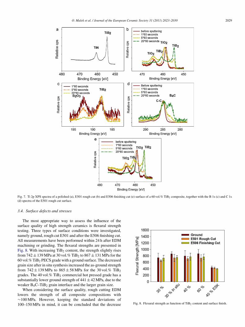
In order to assess the composition of the surface layer,-ray photoelectron spectroscopy (XPS) measurements wereerformed on polished, E501 and E506 surfaces of the 60 vol.%iB2 composite, as summarised in Fig. 7. The Ti 2p spectra of
he polished surface before sputtering, shown in Fig. 7a, revealswo peaks associated with TiB2 at 454.2 and 458 eV.19
The Ti 2p spectra of the E501 rough cutting surface, pre-ented in Fig. 7b, show the presence of TiO2 (459.3 eV) on theop surface. When sputtering deeper into the surface layer, theiB2 peaks from the bulk material start to appear. After 20 minf sputtering, only the bulk material composition is detected.he B 1s spectra (Fig. 7c) show a similar behaviour, with aeak of B2O3 (197.60 eV) which decreases in intensity andventually disappears after 20 min of sputtering. The TiB2 peakn the B 1s spectra (Fig. 7c) slightly increases during sputter-ng and is maximum when the bulk material is reached. In the
1s spectra of Fig. 7d, two peaks can be distinguished. Ini-ially before sputtering, only C–C bonds (284.6 eV) are visible.hese carbon bonds represent an amount of amorphous carbon
n the top layer, introduced by the vacuum system of the XPSeasurement setup. After sputtering, a peak related to B4C
282.8 eV) becomes visible. It is clear that while melting andvaporation are the primary MRM’s in the PECS grades, somexidation takes place as well and the oxides form the recastayer which is visible in the SEM micrographs in Fig. 4. XPSeasurements also showed the presence of substantial quanti-
ies of brass wire deposits in the form of ZnO and Cu2O. Thei 2p spectra of a finished E506 surface resemble the rough
TiB2 peak is already visible before sputtering and the oxideeaks decrease more rapidly, indicating a much thinner recastayer.
O. Malek et al. / Journal of the European Ceramic Society 31 (2011) 2023–2030 2029
F ing cut (e) surface of a 60 vol.% TiB2 composite, together with the B 1s (c) and C 1s(
3
stnAmFf6gfgsw
l∼1
ig. 7. Ti 2p XPS spectra of a polished (a), E501 rough cut (b) and E506 finishd) spectra of the E501 rough cut surface.
.4. Surface defects and stresses
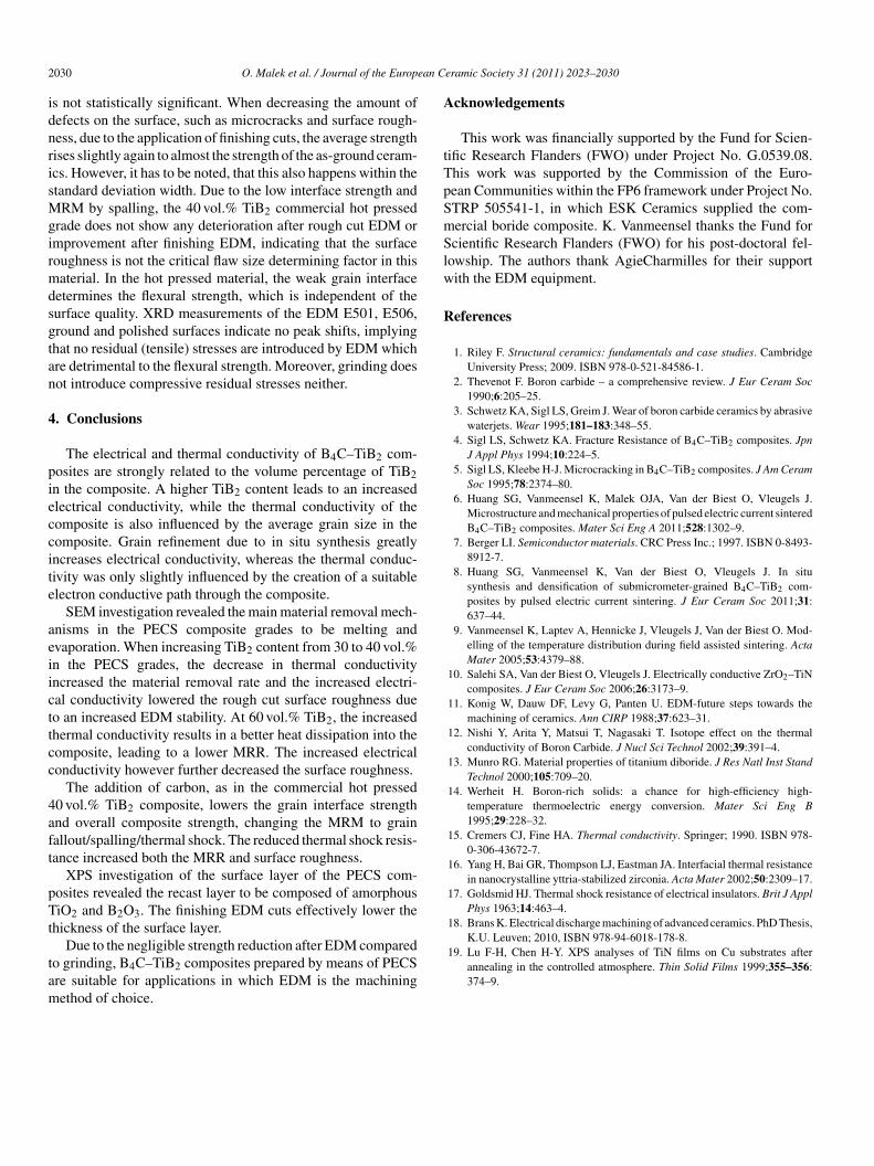
The most appropriate way to assess the influence of theurface quality of high strength ceramics is flexural strengthesting. Three types of surface conditions were investigated,amely ground, rough cut E501 and after the E506 finishing cut.ll measurements have been performed within 24 h after EDMachining or grinding. The flexural strengths are presented inig. 8. With increasing TiB2 content, the strength slightly risesrom 742 ± 139 MPa at 30 vol.% TiB2 to 867 ± 131 MPa for the0 vol.% TiB2 PECS grade with a ground surface. The decreasedrain size after in situ synthesis increased the as-ground strengthrom 742 ± 139 MPa to 865 ± 58 MPa for the 30 vol.% TiB2rades. The 40 vol.% TiB2 commercial hot pressed grade has aubstantially lower ground strength of 441 ± 42 MPa, due to theeaker B4C–TiB2 grain interface and the larger grain size.
When considering the surface quality, rough cutting EDMowers the strength of all composite compositions with100 MPa. However, keeping the standard deviations of
00–150 MPa in mind, it can be concluded that the decrease Fig. 8. Flexural strength as function of TiB2 content and surface finish.
2 ean C
idnrisMgirmdsgtan
4
pieccite
aeiicttcc
4aft
pTt
tam
A
tTpSmSlw
R
K.U. Leuven; 2010, ISBN 978-94-6018-178-8.
030 O. Malek et al. / Journal of the Europ
s not statistically significant. When decreasing the amount ofefects on the surface, such as microcracks and surface rough-ess, due to the application of finishing cuts, the average strengthises slightly again to almost the strength of the as-ground ceram-cs. However, it has to be noted, that this also happens within thetandard deviation width. Due to the low interface strength and
RM by spalling, the 40 vol.% TiB2 commercial hot pressedrade does not show any deterioration after rough cut EDM ormprovement after finishing EDM, indicating that the surfaceoughness is not the critical flaw size determining factor in thisaterial. In the hot pressed material, the weak grain interface
etermines the flexural strength, which is independent of theurface quality. XRD measurements of the EDM E501, E506,round and polished surfaces indicate no peak shifts, implyinghat no residual (tensile) stresses are introduced by EDM whichre detrimental to the flexural strength. Moreover, grinding doesot introduce compressive residual stresses neither.
. Conclusions
The electrical and thermal conductivity of B4C–TiB2 com-osites are strongly related to the volume percentage of TiB2n the composite. A higher TiB2 content leads to an increasedlectrical conductivity, while the thermal conductivity of theomposite is also influenced by the average grain size in theomposite. Grain refinement due to in situ synthesis greatlyncreases electrical conductivity, whereas the thermal conduc-ivity was only slightly influenced by the creation of a suitablelectron conductive path through the composite.
SEM investigation revealed the main material removal mech-nisms in the PECS composite grades to be melting andvaporation. When increasing TiB2 content from 30 to 40 vol.%n the PECS grades, the decrease in thermal conductivityncreased the material removal rate and the increased electri-al conductivity lowered the rough cut surface roughness dueo an increased EDM stability. At 60 vol.% TiB2, the increasedhermal conductivity results in a better heat dissipation into theomposite, leading to a lower MRR. The increased electricalonductivity however further decreased the surface roughness.
The addition of carbon, as in the commercial hot pressed0 vol.% TiB2 composite, lowers the grain interface strengthnd overall composite strength, changing the MRM to grainallout/spalling/thermal shock. The reduced thermal shock resis-ance increased both the MRR and surface roughness.
XPS investigation of the surface layer of the PECS com-osites revealed the recast layer to be composed of amorphousiO2 and B2O3. The finishing EDM cuts effectively lower the
hickness of the surface layer.
Due to the negligible strength reduction after EDM comparedo grinding, B4C–TiB2 composites prepared by means of PECSre suitable for applications in which EDM is the machiningethod of choice.
eramic Society 31 (2011) 2023–2030
cknowledgements
This work was financially supported by the Fund for Scien-ific Research Flanders (FWO) under Project No. G.0539.08.his work was supported by the Commission of the Euro-ean Communities within the FP6 framework under Project No.TRP 505541-1, in which ESK Ceramics supplied the com-ercial boride composite. K. Vanmeensel thanks the Fund forcientific Research Flanders (FWO) for his post-doctoral fel-
owship. The authors thank AgieCharmilles for their supportith the EDM equipment.
eferences
1. Riley F. Structural ceramics: fundamentals and case studies. CambridgeUniversity Press; 2009. ISBN 978-0-521-84586-1.
2. Thevenot F. Boron carbide – a comprehensive review. J Eur Ceram Soc1990;6:205–25.
3. Schwetz KA, Sigl LS, Greim J. Wear of boron carbide ceramics by abrasivewaterjets. Wear 1995;181–183:348–55.
4. Sigl LS, Schwetz KA. Fracture Resistance of B4C–TiB2 composites. JpnJ Appl Phys 1994;10:224–5.
5. Sigl LS, Kleebe H-J. Microcracking in B4C–TiB2 composites. J Am CeramSoc 1995;78:2374–80.
6. Huang SG, Vanmeensel K, Malek OJA, Van der Biest O, Vleugels J.Microstructure and mechanical properties of pulsed electric current sinteredB4C–TiB2 composites. Mater Sci Eng A 2011;528:1302–9.
7. Berger LI. Semiconductor materials. CRC Press Inc.; 1997. ISBN 0-8493-8912-7.
8. Huang SG, Vanmeensel K, Van der Biest O, Vleugels J. In situsynthesis and densification of submicrometer-grained B4C–TiB2 com-posites by pulsed electric current sintering. J Eur Ceram Soc 2011;31:637–44.
9. Vanmeensel K, Laptev A, Hennicke J, Vleugels J, Van der Biest O. Mod-elling of the temperature distribution during field assisted sintering. ActaMater 2005;53:4379–88.
10. Salehi SA, Van der Biest O, Vleugels J. Electrically conductive ZrO2–TiNcomposites. J Eur Ceram Soc 2006;26:3173–9.
11. Konig W, Dauw DF, Levy G, Panten U. EDM-future steps towards themachining of ceramics. Ann CIRP 1988;37:623–31.
12. Nishi Y, Arita Y, Matsui T, Nagasaki T. Isotope effect on the thermalconductivity of Boron Carbide. J Nucl Sci Technol 2002;39:391–4.
13. Munro RG. Material properties of titanium diboride. J Res Natl Inst StandTechnol 2000;105:709–20.
14. Werheit H. Boron-rich solids: a chance for high-efficiency high-temperature thermoelectric energy conversion. Mater Sci Eng B1995;29:228–32.
15. Cremers CJ, Fine HA. Thermal conductivity. Springer; 1990. ISBN 978-0-306-43672-7.
16. Yang H, Bai GR, Thompson LJ, Eastman JA. Interfacial thermal resistancein nanocrystalline yttria-stabilized zirconia. Acta Mater 2002;50:2309–17.
17. Goldsmid HJ. Thermal shock resistance of electrical insulators. Brit J ApplPhys 1963;14:463–4.
18. Brans K. Electrical discharge machining of advanced ceramics. PhD Thesis,
19. Lu F-H, Chen H-Y. XPS analyses of TiN films on Cu substrates afterannealing in the controlled atmosphere. Thin Solid Films 1999;355–356:374–9.
Related Documents