ELEC 321 Introduction to Semiconductor Materials and Devices

Welcome message from author
This document is posted to help you gain knowledge. Please leave a comment to let me know what you think about it! Share it to your friends and learn new things together.
Transcript
ELEC 321
Introduction to SemiconductorMaterials and Devices
INTRODUCTION
• The Information Age requires faster, more accurate and less expensive information as the main foundation of new technologies.
• Solid State Electronic and Optoelectronic Devices are designed to receive, process and transmit information, and are the main building blocks to construct the Information Highway.
• Advances could not have been accomplished without semiconductorspresent in all electronic and optoelectronic devices
• The purpose of this course is to provide a good understanding ofphysical properties of semiconductor materials and microelectronic devices which is essential for future electrical engineers

Conductivities in Materials
• Superconductors• Conductors• Semiconductors• Insulators
Why Semiconductors?
• Semiconductors are used in Design and Structures of almost all Solid State Electronics and Optoelectronics Devices.
• These are possible by controlling the electron behavior in solids.
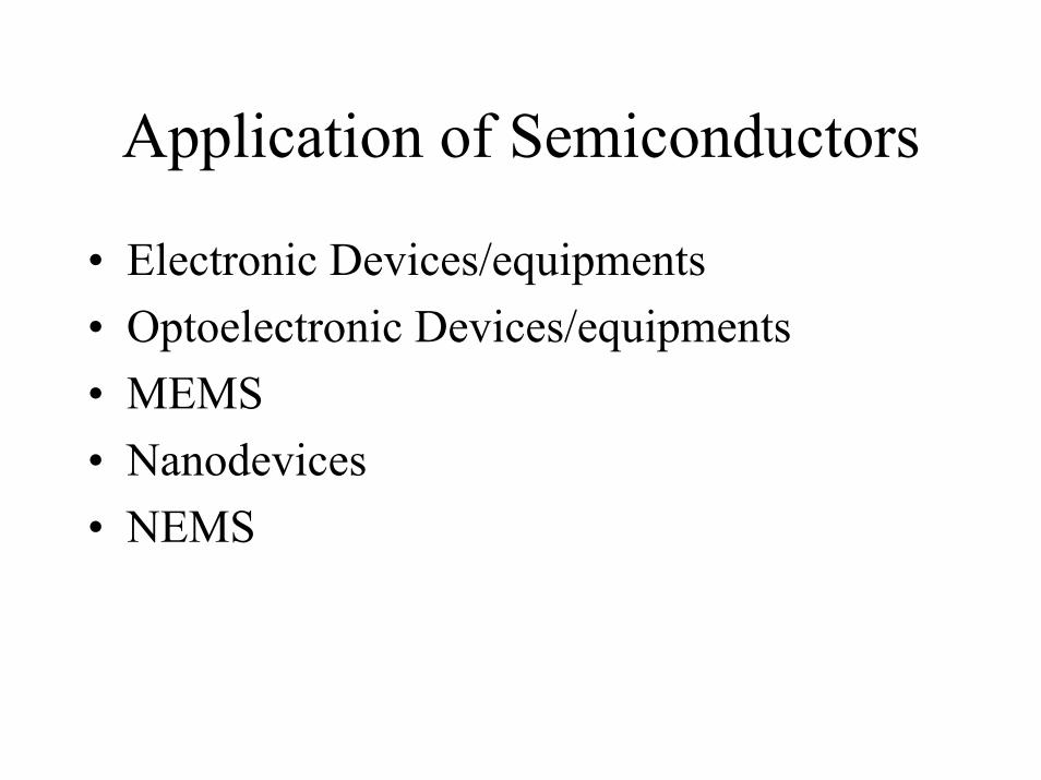
Application of Semiconductors
• Electronic Devices/equipments• Optoelectronic Devices/equipments• MEMS• Nanodevices• NEMS

Classification of Devices
• Combination of Electrics and Mechanics form Micro/Nano-Electro-Mechanical Systems (MEMS/NEMS)
• Combination of Optics, Electrics and Mechanics form Micro/Nano-Opto-Electro-Mechanical Systems (MOEMS/NOEMS)
Optical Electronics
Mechanical
MEMS
MOEMS
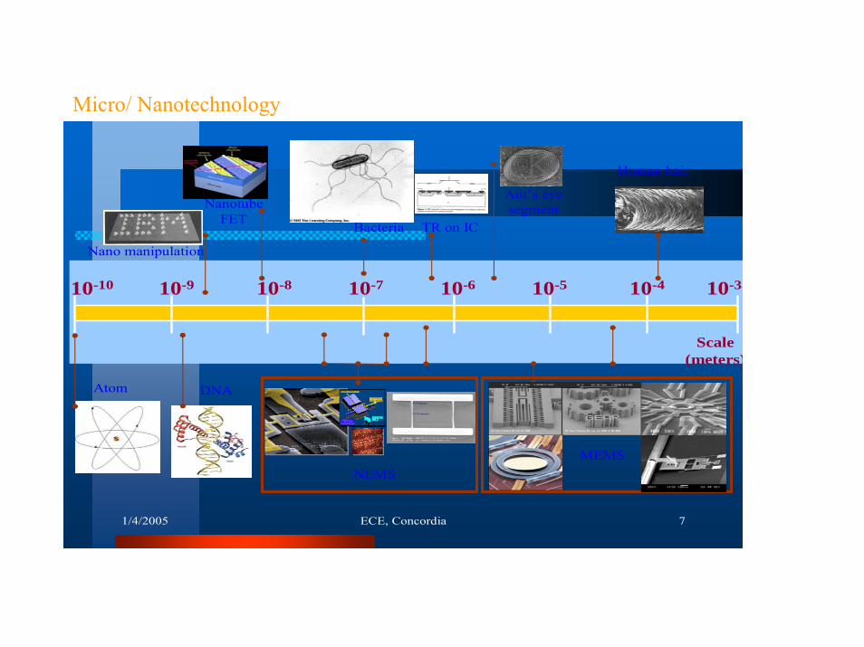
Micro/ Nanotechnology
1/4/2005 ECE, Concordia 7
10-10 10-9 10-8 10-7 10-6 10-5 10-4 10-3
Scale (meters)
Atom DNA
NEMS
Nano manipulation
NanotubeFET
TR on ICBacteria
Human hair
Ant’s eye segment
MEMS
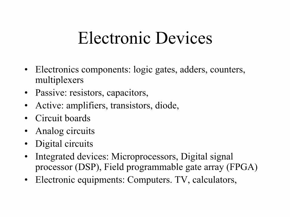
Electronic Devices• Electronics components: logic gates, adders, counters,
multiplexers• Passive: resistors, capacitors, • Active: amplifiers, transistors, diode,• Circuit boards • Analog circuits• Digital circuits• Integrated devices: Microprocessors, Digital signal
processor (DSP), Field programmable gate array (FPGA)• Electronic equipments: Computers. TV, calculators,

Microelectronic ComponentsDiodes
Transistors
Capacitors
Memories
Amplifiers
Switches
Analog & Digital IC

Microelectronics

Schematic illustration of the the structure of a double heterojunction stripecontact laser diode
Oxide insulator
Stripe electrode
SubstrateElectrode
Active region where J > Jth.(Emission region)
p-GaAs (Contacting layer)
n-GaAs (Substrate)
p-GaAs (Active layer)
Currentpaths
L
W
Cleaved reflecting surfaceEllipticallaserbeam
p-AlxGa1-xAs (Confining layer)
n-AlxGa1-xAs (Confining layer) 12 3
Cleaved reflecting surface
Substrate
© 1999 S.O. Kasap, Optoelectronics (Prentice Hall)
Optical Sources; Laser, LED
Switches
Photodiodes
Photodetectors
Solar Cells
Optoelectronic Devices
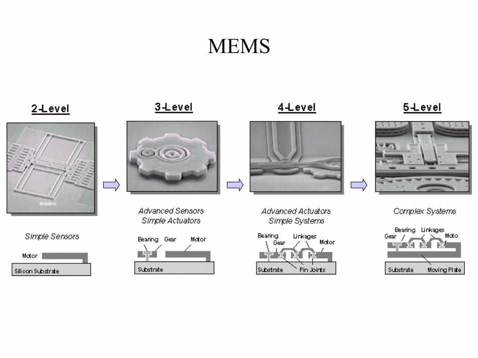
MEMS

MEMS
Hinged positionable mirror
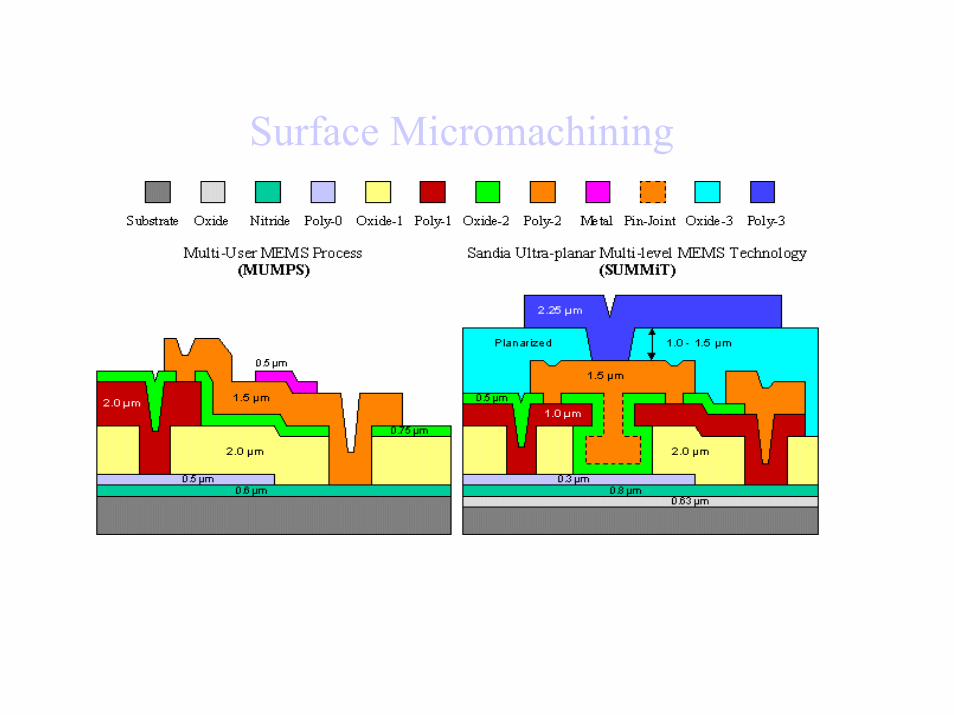
Surface Micromachining
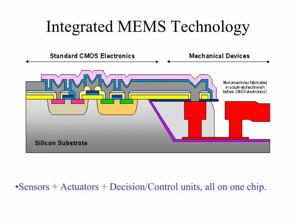
Integrated MEMS Technology
•Sensors + Actuators + Decision/Control units, all on one chip.
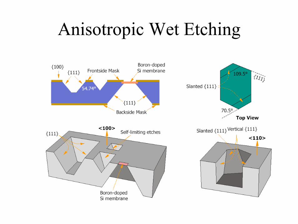
Anisotropic Wet Etching
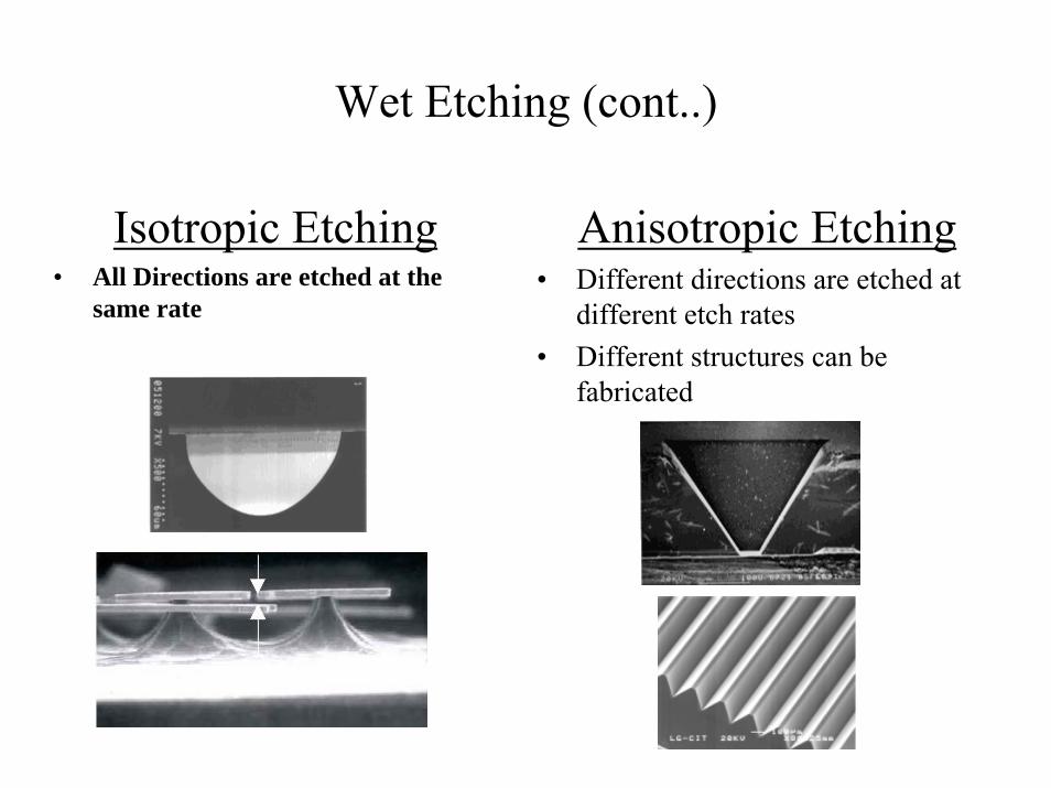
Wet Etching (cont..)
Isotropic Etching• All Directions are etched at the
same rate
Anisotropic Etching• Different directions are etched at
different etch rates• Different structures can be
fabricated

• Anisotropic etching of silicon is one of the key technologies for the fabrication of MEMS/microsystems.
• 3D geometric shapes limited by flat surfaces are formed in the bulk of silicon. Examples: cavities, grooves, and channels.
MEMS heater showing an active free standing membrane released by anisotropic etching.
ConnectionsMembrane
Heater
Cavity
fiber optic
clip SiN
cavity
Fiber optics alignment in grooves of silicon
Better control of the technique is necessary to achieve more complex structures.
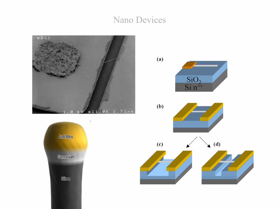
Nano Devices

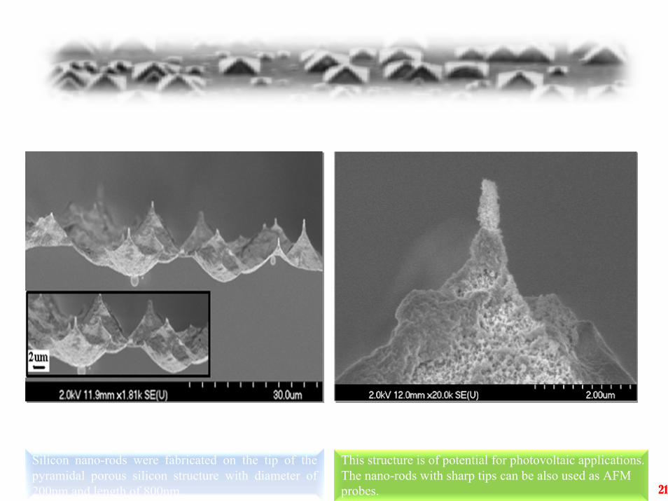
The mentioned textured silicon was electrochemically etched using the same anodization conditions as sampl#7 (I=85mA, t=30min (all conditions are kept constant)).
Silicon nano-rods were fabricated on the tip of the pyramidal porous silicon structure with diameter of 200nm and length of 800nm.
Figure 22-a: Cross section of pyramidal PS fabricated on Si surface of high-concentration hillocks-sample#10.
Figure 22-b: Cross section of one pyramid from sample#10. This image is representing a silicon nano-rod.
This structure is of potential for photovoltaic applications. The nano-rods with sharp tips can be also used as AFM probes. 21

Semiconductor NanoparticlesSemiconductor NanowiresQuantum Dots
• They have potential applications in a number of areas:
• Healthcare and Life Science• Information and Communication Technologies,
Energy applications, solar cells.• Fine Chemicals.• Sensors (chemical, biological, mechanical,…)

Type of Semiconductors
• Simple Semiconductors• Compound Semiconductors• Direct Band gap• Indirect Band gap
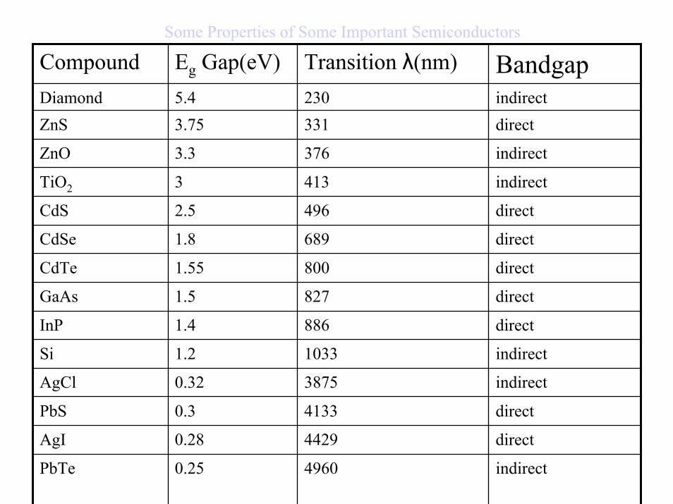
Some Properties of Some Important Semiconductors
Compound Eg Gap(eV) Transition λ(nm) BandgapDiamond 5.4 230 indirectZnS 3.75 331 direct
ZnO 3.3 376 indirect
TiO2 3 413 indirect
CdS 2.5 496 direct
CdSe 1.8 689 direct
CdTe 1.55 800 direct
GaAs 1.5 827 direct
InP 1.4 886 direct
Si 1.2 1033 indirect
AgCl 0.32 3875 indirect
PbS 0.3 4133 direct
AgI 0.28 4429 direct
PbTe 0.25 4960 indirect

Required Knowledge and Background
• In order to understand the behaviour of electrons in solid state materials and how to control them, we need to study the materials structures, and the physics that describe the states of electrons in semiconductors. For this we will go through,
• An introduction to Crystal Structures• An introduction to Quantum Mechanics• A touch of Statistical Physics• Electrons in Solid State Materials• Carrier Transport in Semiconductors• Semiconductors in Equilibrium/Non-Equilibrium States• Basis Structure of pn Junctions (which is the foundation of
almost all electronic and optoelectronic devices).

Silicon Production
• Produced silicon at this stage is 98% pure and is called Metallurgical Grade Silicon (MGS).
• For electronic purposes very high pure silicon - Electronic Grade Silicon (EGS) is needed.
• To obtain EGS from MGS the following reactions are used:
)()()()()( 180016002 gasCOgasSiOliquidSisolidSiOsolidSiC C ++⎯⎯⎯⎯ →⎯+ °−
heatHgasSiHClgasHClsolidSi C ++⎯⎯ →⎯+ °23
300 )()(3)(
)(6)(2)(2)(2 23 gasHClsolidSigasHgasSiHCl +→+
The above process is called chemical vapour deposition (CVD) and the produced Si is polycrystalline and 99.999% pure.

Silicon Wafer
• Type– n-type (e.g.,As,P, Bi
doping)– P-type (B, Ga, In doping)
• Orientation
– {100}, {111},…
Crystals
• An IDEAL CRYSTAL is constructed by infinite repetition of identical structure units in space.
• A LATTICE represents a set of points in space that form a periodic structure, where each point sees the same environment. A building block of atoms called the BASIS is then attached to each lattice point yielding the crystal structure.
LATTICE + BASIS = CRYSTAL STRUCTURE• Identical structure units that have small volume are called UNIT CELL• The smallest unit cell is called PRIMITIVE CELL and the cell that is
most convenient to study crystal structures is called CONVENTIONAL UNIT CELL.
• Unit cells contain all the structural and physical properties of the crystal and ARE NOT unique entities.
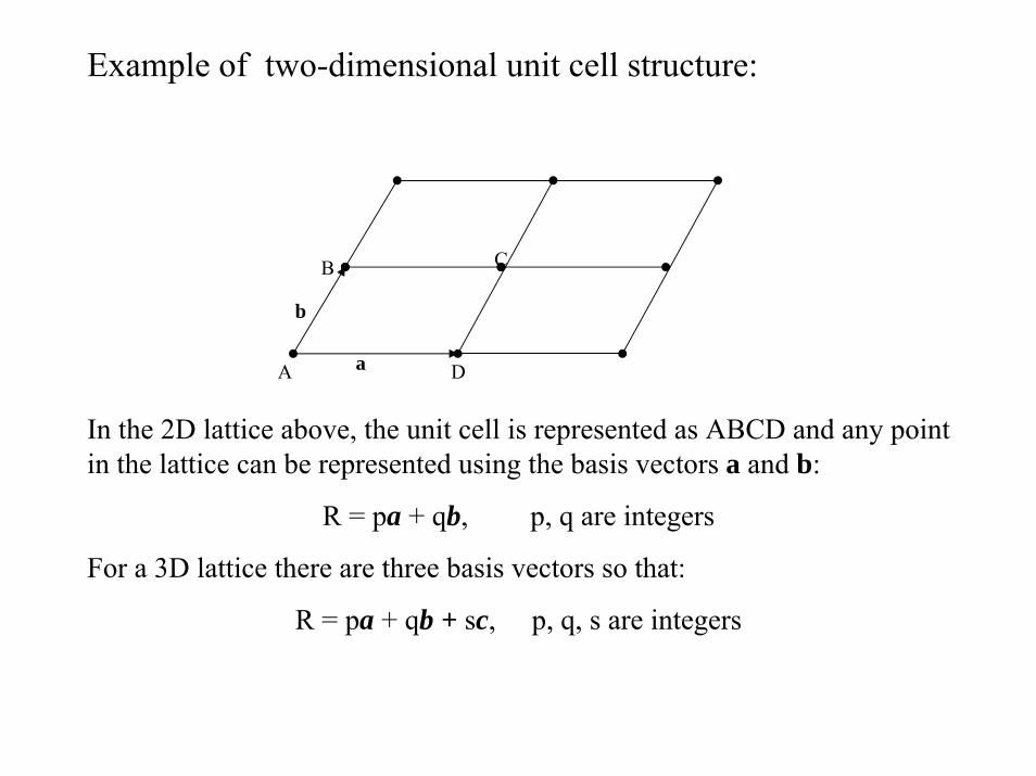
Example of two-dimensional unit cell structure:
A D
CB
a
b
In the 2D lattice above, the unit cell is represented as ABCD and any point in the lattice can be represented using the basis vectors a and b:
R = pa + qb, p, q are integers
For a 3D lattice there are three basis vectors so that:
R = pa + qb + sc, p, q, s are integers
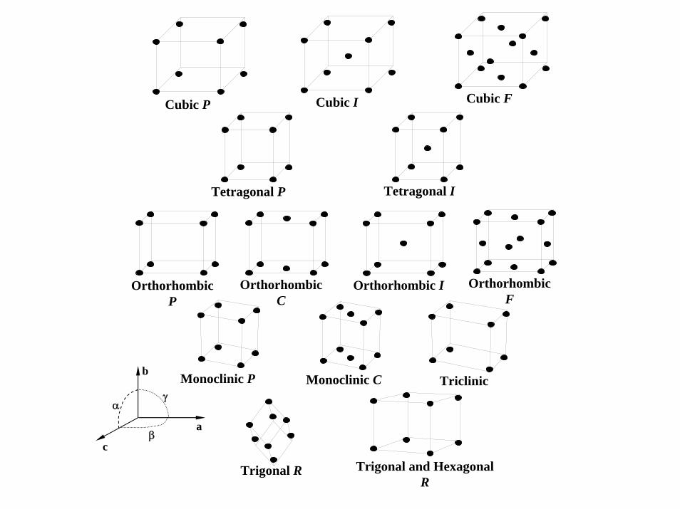
Cubic P Cubic I Cubic F
Tetragonal P Tetragonal I
Orthorhombic P
Orthorhombic C
Orthorhombic I Orthorhombic F
Monoclinic P Monoclinic C Triclinic
Trigonal R Trigonal and Hexagonal R
a
c
b
γ
β
α
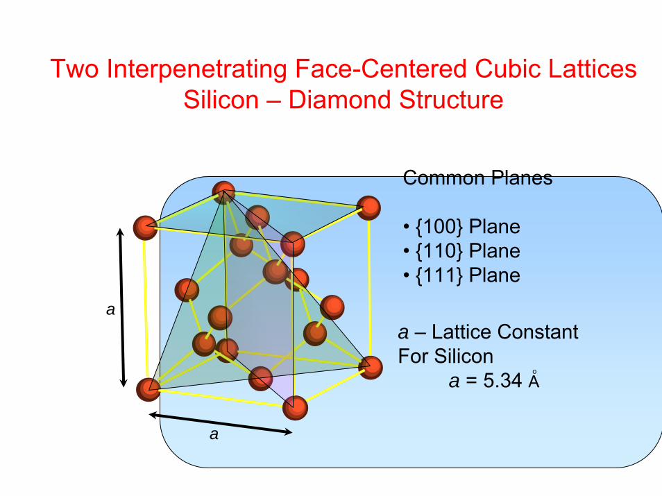
Common Planes
• {100} Plane• {110} Plane• {111} Plane
a
aa – Lattice ConstantFor Silicon
a = 5.34 Ao
Two Interpenetrating Face-Centered Cubic LatticesSilicon – Diamond Structure

Principles of Quantum Mechanics
The principle of Energy Quanta:• Experiments which showed inconsistency between
experimental results and classical theories.– Thermal Radiation– Hydrogen Atoms– Photoelectric Effect
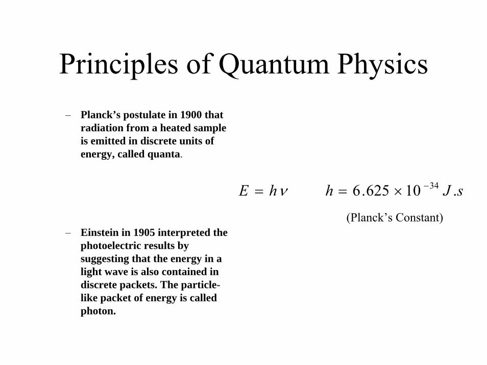
Principles of Quantum Physics– Planck’s postulate in 1900 that
radiation from a heated sample is emitted in discrete units of energy, called quanta.
– Einstein in 1905 interpreted the photoelectric results by suggesting that the energy in a light wave is also contained in discrete packets. The particle-like packet of energy is called photon.
(Planck’s Constant)
sJhhE .10625.6 34−×== ν
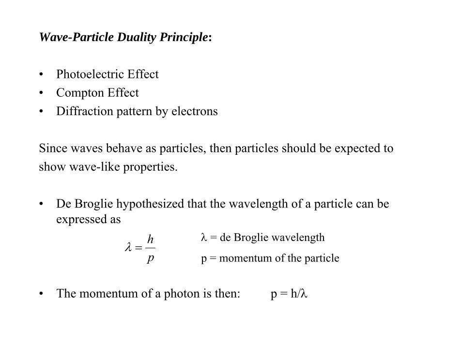
Wave-Particle Duality Principle:
• Photoelectric Effect• Compton Effect• Diffraction pattern by electrons
Since waves behave as particles, then particles should be expected toshow wave-like properties.
• De Broglie hypothesized that the wavelength of a particle can beexpressed as
• The momentum of a photon is then: p = h/λ
ph
=λλ = de Broglie wavelength
p = momentum of the particle

The Uncertainty Principle (Heisenberg)
• It is impossible to simultaneously describe with absolute accuracy the position (energy) and momentum (instant of time) of a particle.
• ħ is very small so this principle only applies to very small particles
Quantum Mechanics does not predict a deterministic course of events, but rather the probabilities of various alternative possible events.
sJhxp .10054.12
34−×==≥ΔΔπ
hh
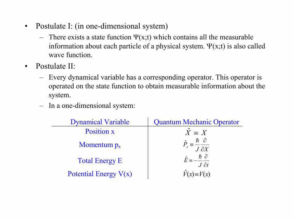
• Postulate I: (in one-dimensional system)– There exists a state function Ψ(x;t) which contains all the measurable
information about each particle of a physical system. Ψ(x;t) is also called wave function.
• Postulate II:– Every dynamical variable has a corresponding operator. This operator is
operated on the state function to obtain measurable information about the system.
– In a one-dimensional system:
Dynamical Variable Quantum Mechanic OperatorPosition x XX ≡ˆ
Momentum px XJPx ∂
∂≡hˆ
Total Energy E tJE
∂∂
−≡hˆ
Potential Energy V(x) )()(ˆ xVxV ≡
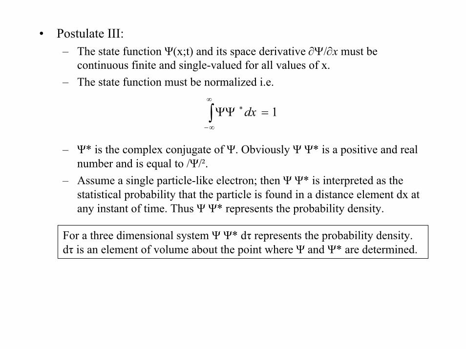
• Postulate III:– The state function Ψ(x;t) and its space derivative ∂Ψ/∂x must be
continuous finite and single-valued for all values of x.– The state function must be normalized i.e.
– Ψ* is the complex conjugate of Ψ. Obviously Ψ Ψ* is a positive and real number and is equal to /Ψ/².
– Assume a single particle-like electron; then Ψ Ψ* is interpreted as the statistical probability that the particle is found in a distance element dx at any instant of time. Thus Ψ Ψ* represents the probability density.
1=ΨΨ∫∞
∞−
∗dx
For a three dimensional system Ψ Ψ* dτ represents the probability density. dτ is an element of volume about the point where Ψ and Ψ* are determined.

• The average value ⟨Q⟩ of any variable corresponding to the state function Ψ is given by expectation value:
• ⟨Q⟩ is the expected value of many observations.
• Once the state function corresponding to any particle was found, it was possible to calculate the average position, energy and momentum of the particle within the limit of the uncertainty principle.
∫∞
∞−
∗ ΨΨ= τdQQ ˆ

Principles of QM
• Schrodinger Wave Equation• Physical meaning and its application• Some examples: infinite potential well,
potential step function, potential barrier…• Tunneling Effect

Quantum Well
2
222
2manEn
h π=
222
4
2)4( n
qmE
o
on
hπε
−=
0/2/3
0100
11 arqa
−⎟⎟⎠
⎞⎜⎜⎝
⎛=
πψ
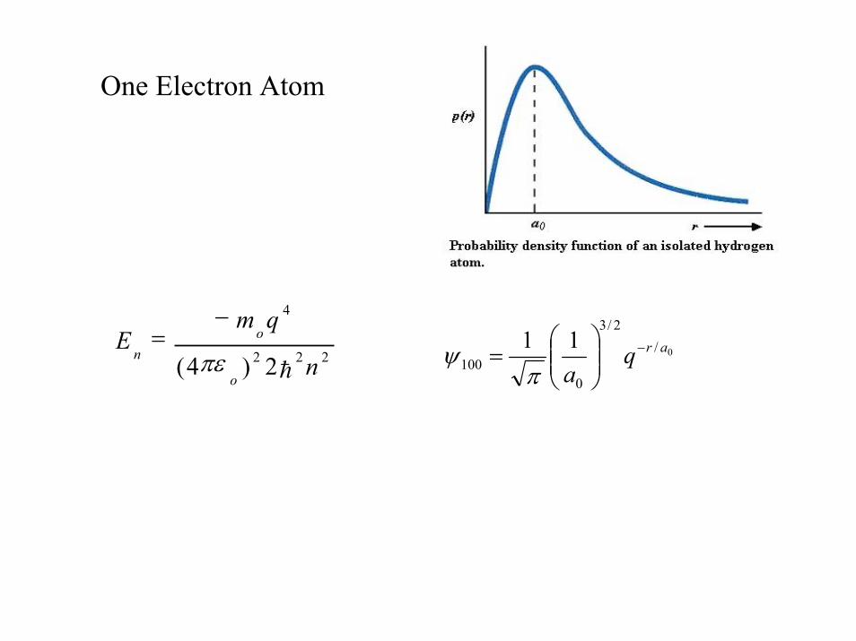
One Electron Atom
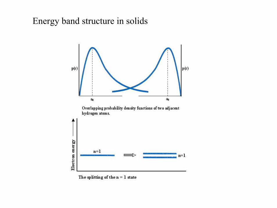
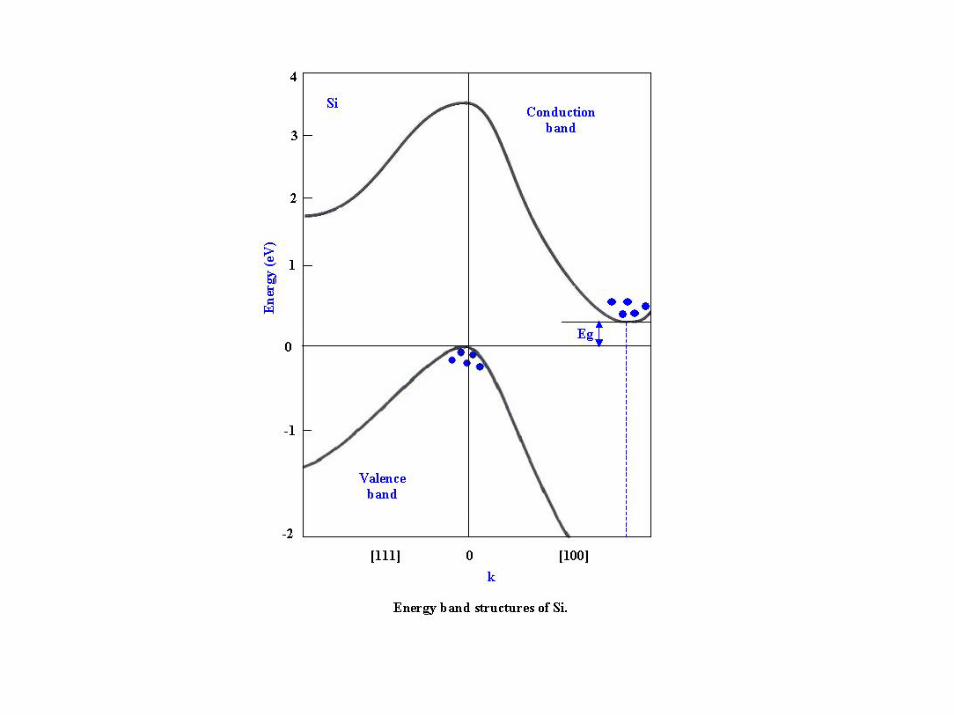
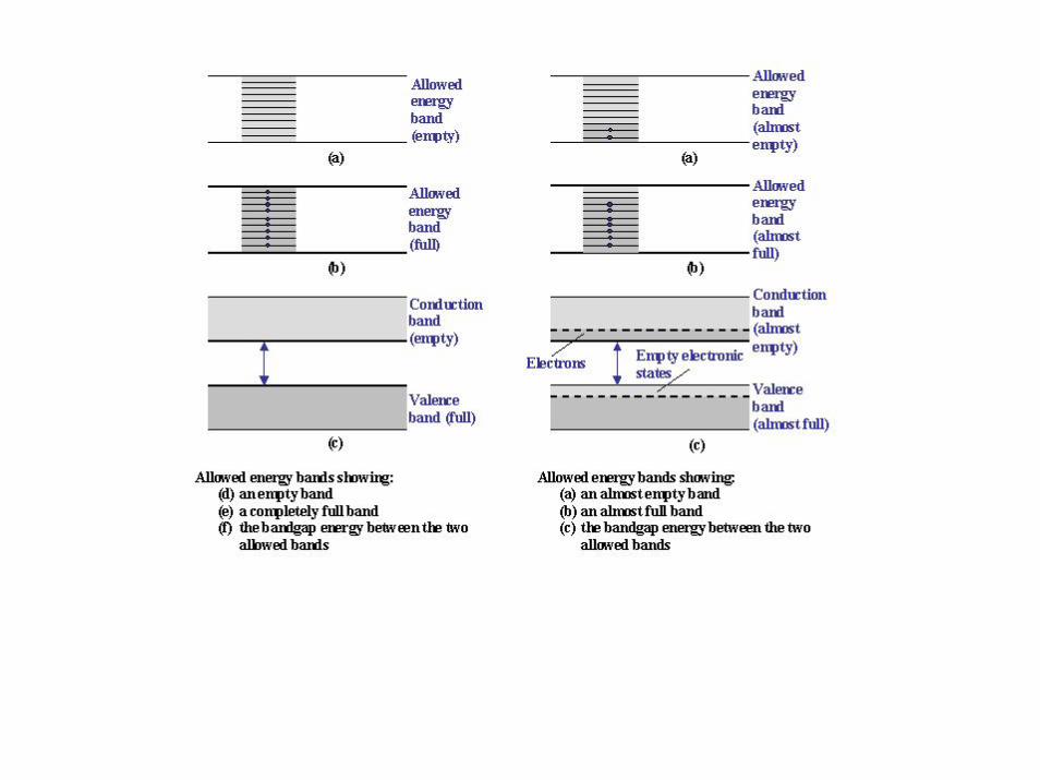
Energy band structure in solids

1s
2s
2p
1s
2s
2p
1s
2s
2p
1s
2s
2p
1s
The potential wells due to the interactions between 2 atoms (in one molecule). Some
electrons are shared between the atoms. Due to the interactions between electrons-
electrons, nucleons-nucleons, and electrons-nucleons, the energy levels split, creating 1s,
2s, 2p,… doublets.
The potential experienced by an electron due to the coulombinteractions around an atom. 1s, 2s, 2p,… are the energy
levels that the electron can occupy.
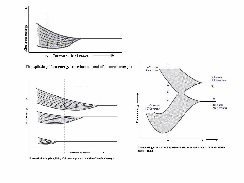
Larger molecules, larger splitting.
In Solid with n≈ 1023 atoms, the sublevels are extremely close to each other. They coalesce and form an energy band. 1s, 2s, 2p… energy bands.

Periodical Potential
r
r
Non-Periodical Potential
r
r
)(rV
2)(rΨ
)(rV
2)(rΨ
jkrerur ⋅=Ψ )()(
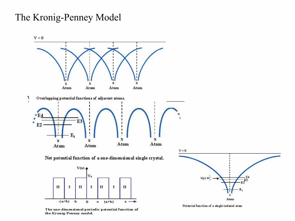
The Kronig-Penney Model


The Concepts of:
1) Effective Mass
*2
2
2
11mdk
Ed=
h
2) Negative Mass
3) Positive charge
4) Holes

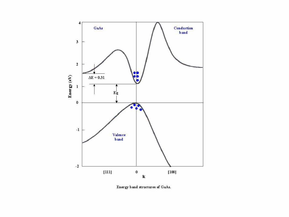
Atomic Bonding in Semiconductors
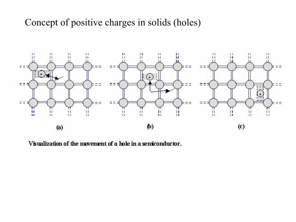
Concept of positive charges in solids (holes)

EEhm
Eg
EEhmEg
vp
v
cn
c
−=
−=
3
2/3*
3
2/3*
)2(4)(
)2(4)(
π
π
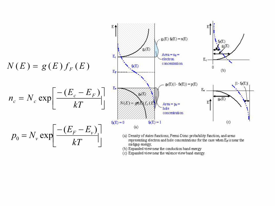
Density of State.
Electrons Distribution.
⎟⎠⎞
⎜⎝⎛ −
+=
kTEE
EfF
F
exp1
1)(
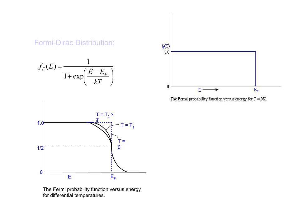
Fermi-Dirac Distribution:
E EF
0
1/2
1.0
T = 0
T = T1
T = T2 > T1
The Fermi probability function versus energy for differential temperatures.
nn
⎥⎦⎤
⎢⎣⎡ −−
=kT
EENp vFv
)(exp0
⎥⎦⎤
⎢⎣⎡ −−
=kT
EENn Fccc
)(exp)()()( EfEgEN F=
)()()( EfEgEN F=
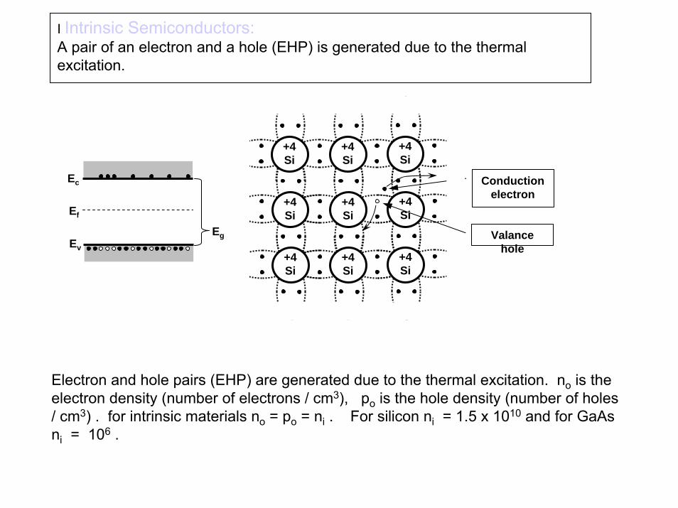
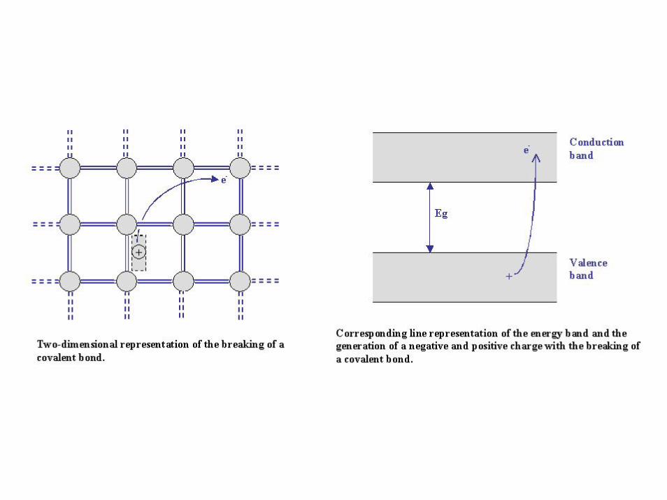
I Intrinsic Semiconductors:A pair of an electron and a hole (EHP) is generated due to the thermal excitation.
Conduction electron+4
Si+4Si
+4Si
+4Si
+4Si
+4Si
+4Si
+4Si
+4Si
Eg
Ec
Ev
Ef
Valance hole
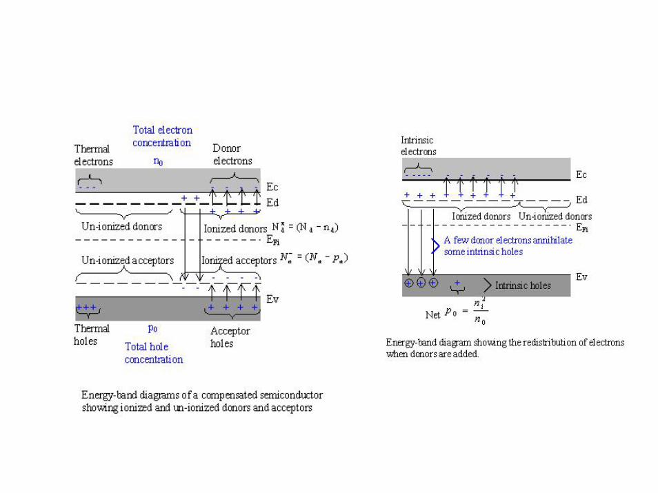
Electron and hole pairs (EHP) are generated due to the thermal excitation. no is the electron density (number of electrons / cm3), po is the hole density (number of holes / cm3) . for intrinsic materials no = po = ni . For silicon ni = 1.5 x 10¹⁰ and for GaAsni = 106 .
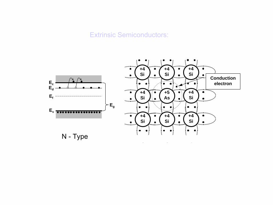
Extrinsic Semiconductors:
+5As
+4Si
+4Si
+4Si
+4Si
+4Si
+4Si
+4Si
+4Si
Eg
Ec
Ev
Ef
Ed
Conduction electron
N - Type
+3Al
+4Si
+4Si
+4Si
+4Si
+4Si
+4Si
+4Si
+4Si
Eg
Ec
Ev
Ef
Valence hole
Ea
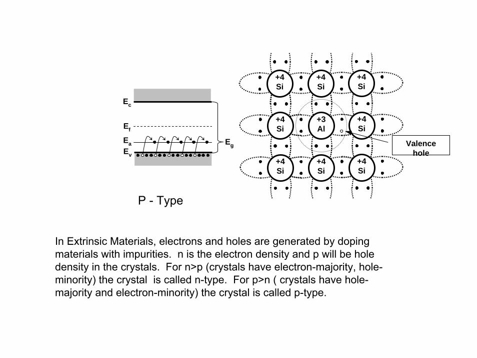
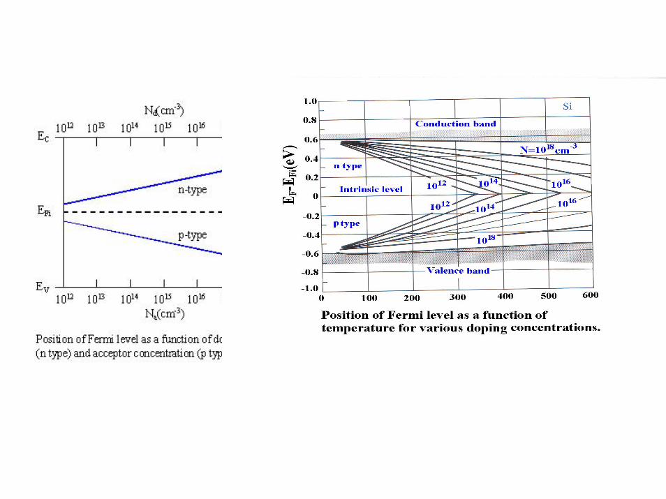
In Extrinsic Materials, electrons and holes are generated by doping materials with impurities. n is the electron density and p will be hole density in the crystals. For n>p (crystals have electron-majority, hole-minority) the crystal is called n-type. For p>n ( crystals have hole-majority and electron-minority) the crystal is called p-type.
P - Type

⎥⎦⎤
⎢⎣⎡ −−
=kT
EEnp FiFi
)(exp0 ⎥⎦⎤
⎢⎣⎡ −
=kT
EEnn FiFi
)(exp0
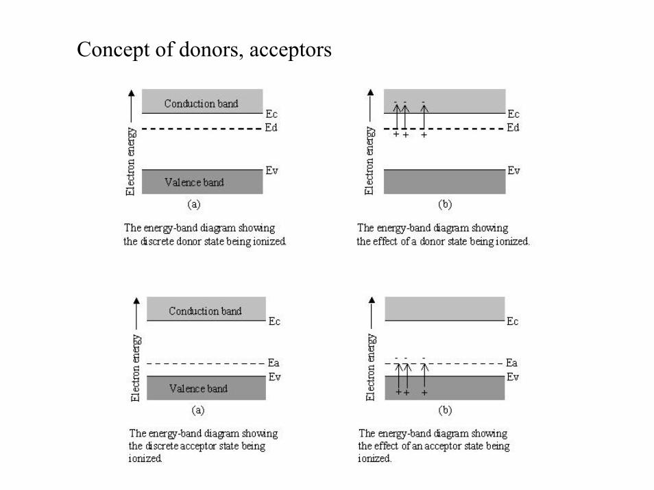
Concept of donors, acceptors


Carrier Transport:
Current in Semiconductors: (Drift, Diffusion, Carriers Recommendation, Carriers Generation)
Drift Current:
EpnqJ pndrf )( μμ +=

Diffusion current:
dxdpqDJ
dxdnqDJ
ppdif
nndif
−=
=
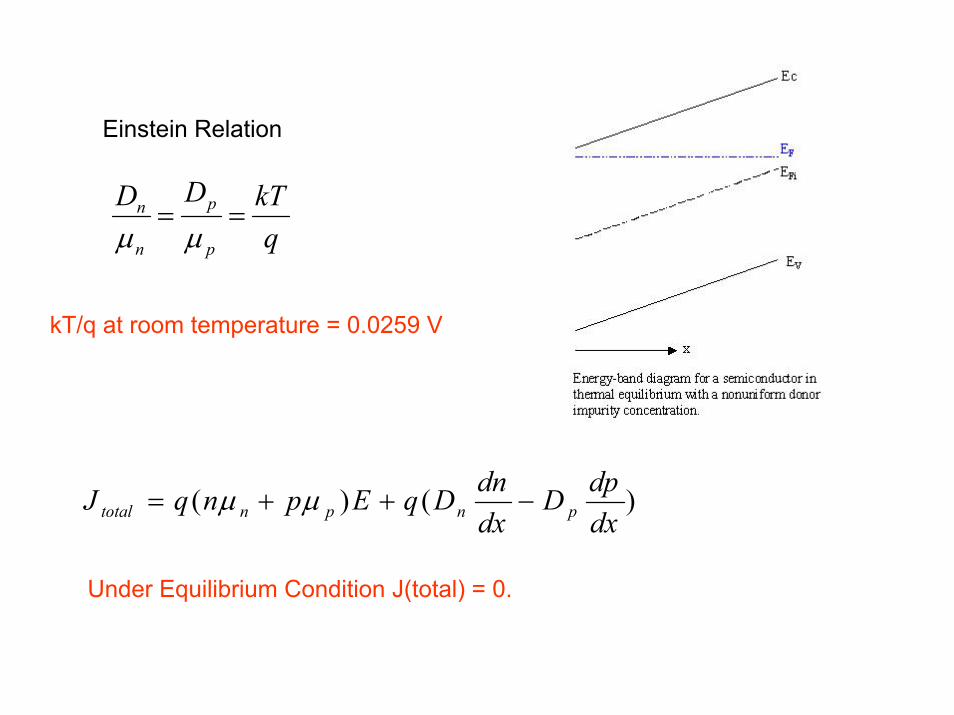
)()(dxdpD
dxdnDqEpnqJ pnpntotal −++= μμ
Under Equilibrium Condition J(total) = 0.
qkTDD
p
p
n
n ==μμ
Einstein Relation
kT/q at room temperature = 0.0259 V
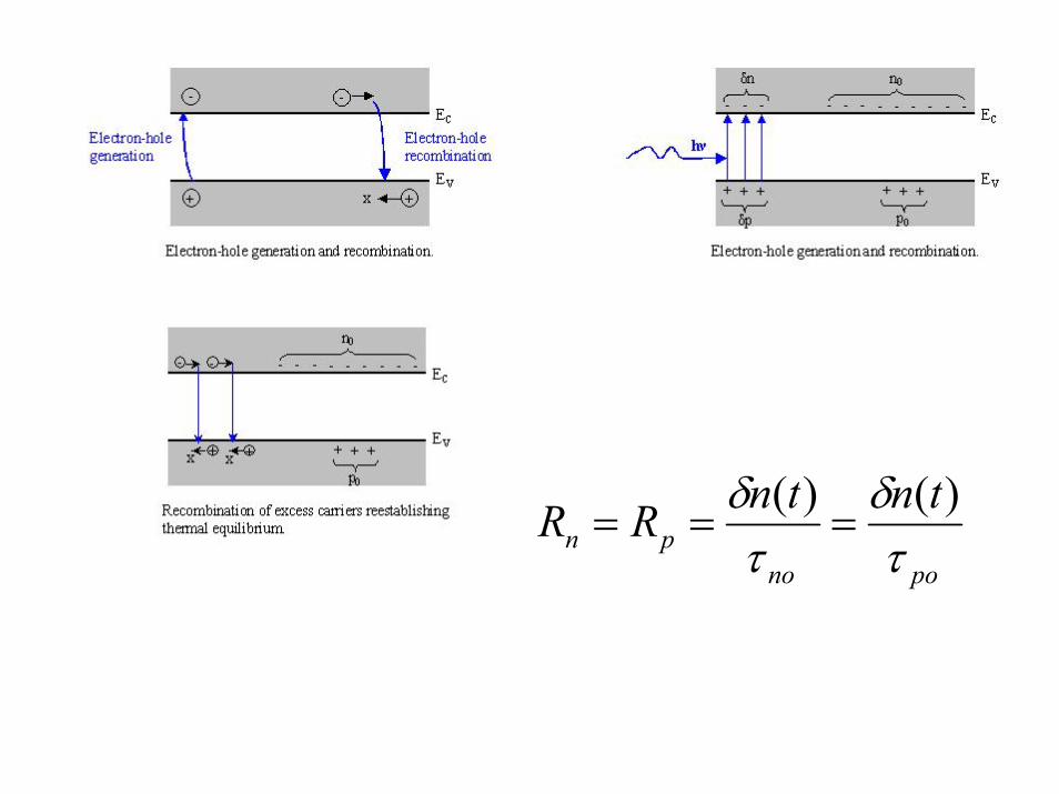
ponopn
tntnRRτδ
τδ )()(
===

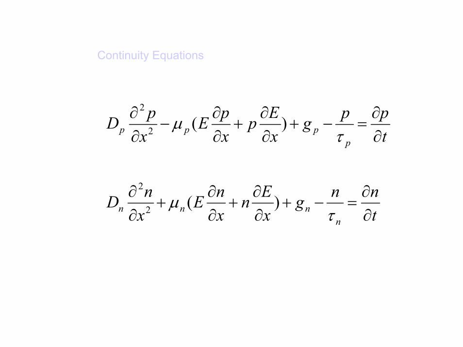
tnng
xEn
xnE
xnD
tppg
xEp
xpE
xpD
nnnn
pppp
∂∂
=−+∂∂
+∂∂
+∂∂
∂∂
=−+∂∂
+∂∂
−∂∂
τμ
τμ
)(
)(
2
2
2
2
Continuity Equations

Surface Effects
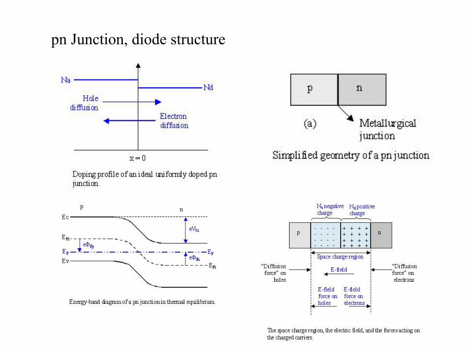
pn Junction, diode structure

pn junction under biased conditions
Related Documents