Assoc. Prof. Dr. Mohamed Ragaa Balboul ELCT 705 : Semiconductor Technology Lecture 04: Crystal Growth and Wafer Fabrication (CZ Crystal Growth) Department of Electronic and Electrical Engineering

Welcome message from author
This document is posted to help you gain knowledge. Please leave a comment to let me know what you think about it! Share it to your friends and learn new things together.
Transcript

Assoc. Prof. Dr. Mohamed Ragaa Balboul
ELCT 705 :Semiconductor Technology
Lecture 04: Crystal Growth and Wafer Fabrication (CZ Crystal Growth)
Department of Electronic and Electrical Engineering
Types of Solids
The three general types of solids are
Amorphous Polycrystalline Single-Crystal
Order only within a few atomic or molecular
dimensions.
High degree of order over many atomic or
molecular dimensions.
High degree of order throughout the entire volume of the material.

Atomic hard sphere model
Unit CellUnit cell is the smallest unit of volume that permits identical cells to be stacked together to fill all space.
By repeating the pattern of the unit cell over and over in all directions, the entire crystal lattice can be constructed.
CRYSTAL FACES

Unit CellThe vectors and define a unit cell, which can generate the entire lattice by repeated translations. once the unit cell is defined, the rest of the structure is defined as well.Unit cell parameters (a, b, c, α, β, γ ) are chosen to best represent the highest possible symmetry of the lattice.
Lattice is an imaginary pattern
Lattice points
Putting points
at corners
b
c
a
αβγa
b
c

The 14 Bravais Lattices Where Can I Put the Lattice Points? There is a limited number of possibilities !
The French scientist Auguste Bravais, demonstrated that only these 14 types of unit cells are compatible with the orderly arrangements of atoms found in crystals.
Name # Bravaislattice
Conditions
Triclinic 1 a ≠ b≠ c α ≠ β ≠ γ≠ 90o
Monoclinic 2 a ≠ b ≠ c α=β=90° ≠ γ
Orthorombic 4 a ≠ b ≠ c α=β=γ=90°
Hexagonal 1 a = b ≠ c α=β=90° γ=120 °
Rhombohedral 1 a = b = c α=β=γ ≠ 90°
Tetragonal 2 a = b ≠ c α=β=γ=90°
Cubic 3 a = b= c α=β=γ=90°

Cubic SystemThe three crystal structures which determine some of the basic characteristics of these crystals.
>90% of elemental metals crystallize upon solidification into 3 densely packed crystal structures:
Simple Cubic Body-Centered Cubic Face-Centered Cubic
Lat
tice
con
stan
t

Atomic Packing Factor (APF)
Unit cell contains: 8 x 1/8 =1 atom/unit cell
APF for a simple cubic structure = 0.52
a 3
35.0
3
41
a
a
APF
volume
unit cell
atoms
unit cell
Ra 2
APF = (volume of atoms in unit cell*/ volume of unit cell)*assume hard spheres the volume of one atoms is (4/3) r3
maximum packing efficiency for equal-sized spheres
atoms
volume
Lat
tice
con
stan
t

Atomic Packing Factor (APF)Unit cell contains: (6 x ½ )+ (8 x 1/8) = 4 atoms/unit cell
APF for a Face-centered cubic = 0.74
2/4Ra
volume
unit cell
atoms
unit cell
atoms
volume
3
3
4/23
44
a
a
APF
maximum packing efficiency for equal-sized spheres
atoms
volume
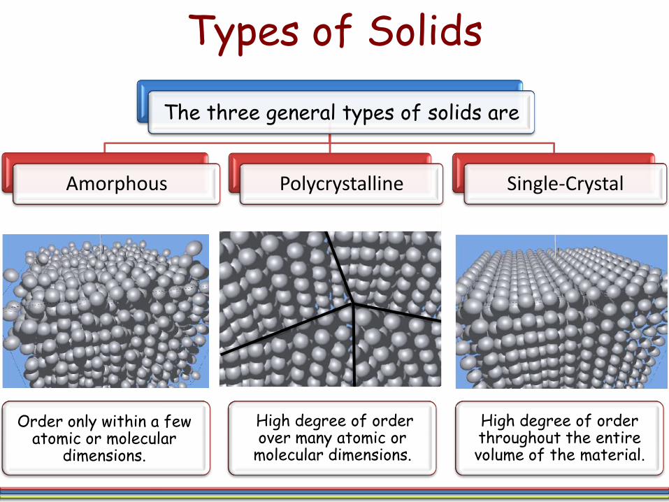
Miller IndicesMiller indices : A shorthand notation to describe certain crystallographic directions and planes in a material. Denoted by brackets. A negative number is represented by a bar over the number.
[hkl] for the direction of a crystal such as [l00] for the x axis.
(hkl) for a plane that intercepts the x axis on the negative side of the origin.
{hkl}for planes of equivalent symmetry such as {l00} for (100), (010), and (001) in cubic symmetry.
hkl for a full set of equivalent directions.
(100)(111)
[100]
[111]

How to Get Miller Indices
Z
y
x
3a
1a
2a
1. Find the intercepts x, y, z of the plane with the three basis axes in terms of the lattice constant
2. Take reciprocals of these number and reduce to the smallest three integers having the same ratio
3. Enclose the result in parentheses (hkl) as Miller indices.
1. Intercepts are 2, 1, 3
2. Reciprocals , ,
3. Clear the fractions (×6) , ,
4. Reduce to lowest term 3, 6, 2
5. Millers are (362)
2
1
1
1
3
1
2
6
1
6
3
6

Inter-planner SpacingThe inter-planar spacing, d (normal distance between two consecutive parallel planes) for a cubic structure is given by
222)(
lkh
ad hkl

Silicon Crystal StructureSilicon has a diamond cubic lattice structure.
This structure is most easily visualized as twomerged FCC lattices with the origin of the second lattice offset from the first by a/4 in all three directions.
Bulk properties in the silicon are generally isotropic (independent of direction) because of the cubic symmetry of the silicon crystal.
(111) Planes in silicon have the largest number of silicon atoms per cm2 comparing with (100) planes.
(111) Planes oxidize faster than (100) since the oxidation rate is proportional to the number of silicon atoms available for reaction.
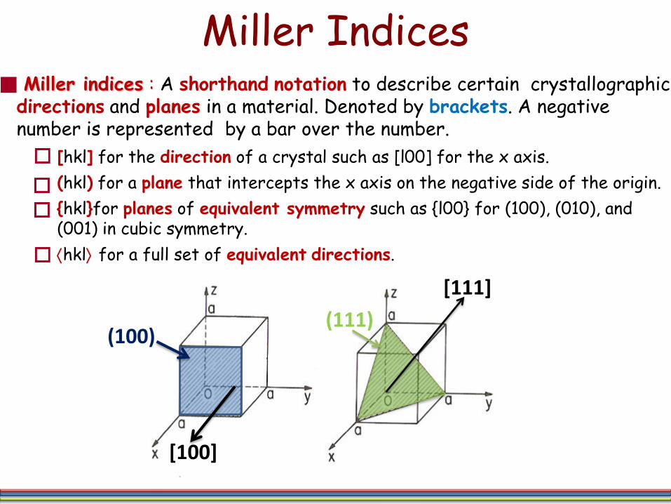
Defects in CrystalsThere are several types of defects such as point defects, line defects , area defects, and volume defects (depending on their dimensionality).
Point defects:
The first is simply a missing silicon lattice atom or vacancy (V).The second is an extra silicon atom (I)
1. An atom sitting unbounded in one of the available sites between silicon atom (interstitial).
2. Two atoms sharing one lattice site, a defect usually referred to as an interstitialcy.
In general, the concentrations of these defect increases as temperature increases.

Defects in CrystalsDislocations
One-dimensional defects in crystals are known as dislocations.
The top part of the crystal contains an extraplane of atom, which terminates at a dislocation.
The dislocation itself is a linear defect in the direction into the depth of the crystals.
Wafers are normally dislocation free, but such defects can be generated during the high temperature steps, particularly if thin films present on the wafer surface generate high stresses.
Dislocations are active defects in crystals, that is they can move when subjected to stresses.

Wafer Fabrication

Raw Materials and PurificationQuartz
Chemically quartzite is SiO2.
The first step is to convert the quartzite to Metallurgical Grade Silicon or MGS; quartzite + carbon source is heated to 2000 oC.
2C (solid) + SiO2 (solid) Si(liquid) + 2CO (gas)
The MGS grade silicon is 98 % pure.
The second step is to convert the MGS to Electronic Grade Silicon (EGS), usually by grinding the MGS to a fine powder and then reacting it with gaseous HCl(Hydrochloric acid) at elevated temperature; the product is SiHCl compounds.
2SiHCl3 (gas) + 2H2 (gas) 2Si(solid) + 6HCl (gas)
This is accomplished in large CVD reactor. The EGSis ultrapure polycrystalline silicon.

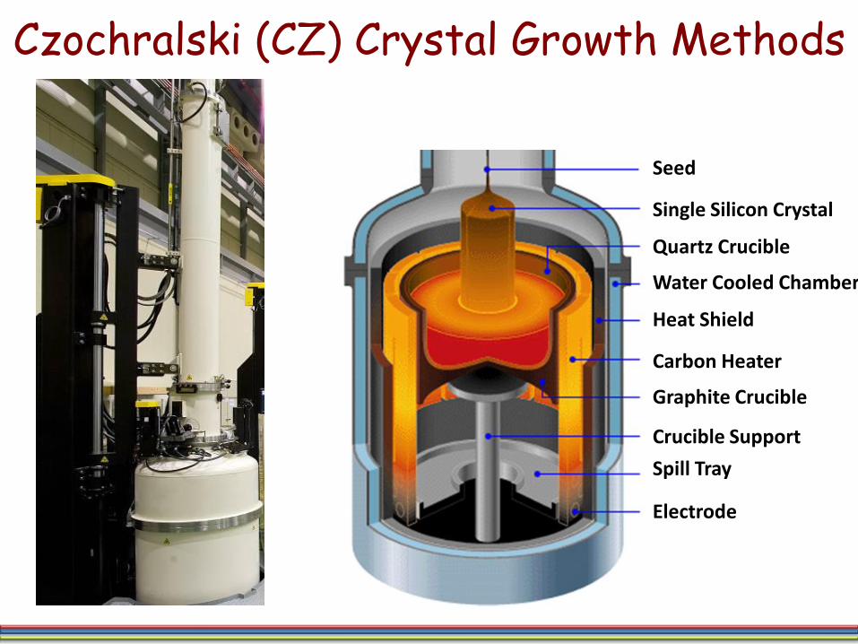
Czochralski (CZ) Crystal growth
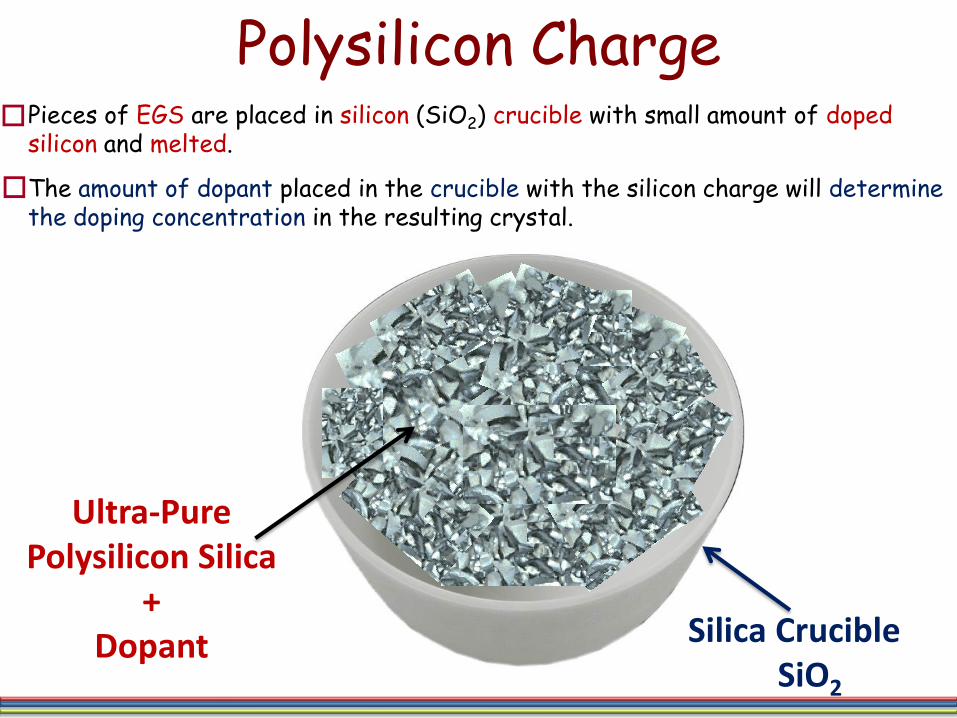
Polysilicon Charge
Silica CrucibleSiO2
Ultra-Pure Polysilicon Silica
+Dopant
Pieces of EGS are placed in silicon (SiO2) crucible with small amount of dopedsilicon and melted.
The amount of dopant placed in the crucible with the silicon charge will determine the doping concentration in the resulting crystal.

Seed Dipping to the MeltThe melt temperature is stabilized at just above the silicon melting point (1417 oC).
A single-crystal seed is then lowered into the melt.
The crystal orientation of this seed will determine the orientation of the resulting wafers.

Shoulder GrowthThe seed is then slowly pulled out of the melt.
Silicon atoms from the melt bond to the atoms in the seed, lattice plane by lattice plane, forming a single crystal as the seed is pulled upwards.
The diameter of the resulting crystal is controlled by the rate of pulling.

Start of Body GrowthDuring CZ crystal growth, the seed and the crucible are normally rotated in opposite directions to promote mixing in the liquid and more uniform growth.
This also has the effect of increasing the corrosion of the crucible by melt; silicon and oxygen being incorporated into melt.
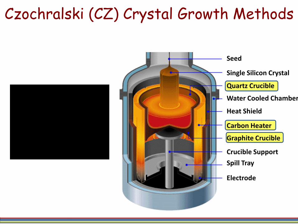
Czochralski (CZ) Crystal Growth Methods
Seed
Single Silicon Crystal
Quartz Crucible
Water Cooled Chamber
Heat Shield
Carbon Heater
Graphite Crucible
Crucible Support
Spill Tray
Electrode
Czochralski (CZ) Crystal Growth Methods
Seed
Single Silicon Crystal
Quartz Crucible
Water Cooled Chamber
Heat Shield
Carbon Heater
Graphite Crucible
Crucible Support
Spill Tray
Electrode

Wafer Preparation and Specification
The process begins with shaping the grown crystal to uniform diameter.
The crystal is normally grown slightly oversized and then trimmed to the final diameter.
The next step is the actual sawing of the ingot into individual wafer (Slicing).
This is usually accomplished with a rotating diamond-tipped blade that cuts on its inside edge.
200 mm diameter wafers today are usually about 725 mm thick in their final finished form.
The final step is to produce a mirror finish on one surface. A two step process is used, chemical etching, followed by chemical mechanical polishing.
The process removes the surface layers containing damage from the various mechanical operations performed earlier.
This step producing a surface which is defect free and with mirror finish.

Czochralski (CZ) Crystal Growth
The relationship between the pull rate and the crystal diameter.
Freezing occurs between isotherms (constant temperature) X1 (liquid) and X2 (Solid).
During the freezing process , heat is released to allow the silicon to transform from the liquid to solid state (the heat of fusion).
Freezing zone

Heat BalanceThis heat must be removed from the freezing interface, a process that occurs primarily by heat conduction up the solid crystal .
Heat balance: latent heat of crystallization + heat conducted from melt to crystal = heat conducted away. Thus we may write
2
2
1
1
Adx
dTkA
dx
dTk
dt
dmL SL
L = Latent heat of fusion
KL = Thermal conductivity of liquid
KS= Thermal conductivity of solid
A1 and A2 are the cross-section areas.
= Amount of silicon freezing per unit timedt
dm
= Thermal gradient at isotherm x1
1dx
dT
= Thermal gradient at isotherm x2
2dx
dT
The middle term, which will neglected, represents any additional heat that may flow from the liquid to the solid because of the temperature gradients.
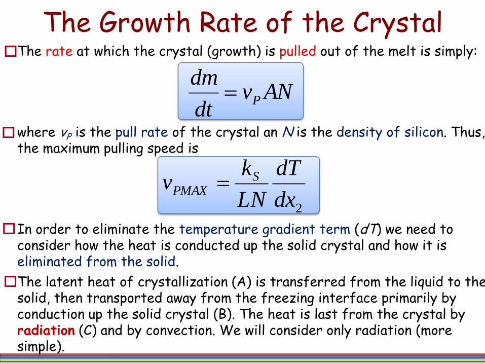
The Growth Rate of the CrystalThe rate at which the crystal (growth) is pulled out of the melt is simply:
where vP is the pull rate of the crystal an N is the density of silicon. Thus, the maximum pulling speed is
In order to eliminate the temperature gradient term (dT) we need to consider how the heat is conducted up the solid crystal and how it is eliminated from the solid.
The latent heat of crystallization (A) is transferred from the liquid to the solid, then transported away from the freezing interface primarily by conduction up the solid crystal (B). The heat is last from the crystal by radiation (C) and by convection. We will consider only radiation (more simple).
ANvdt
dmP
2dx
dT
LN
kv S
PMAX

Heat Losses due to RadiationThe Stefan-Boltzmann law describes heat loss due to radiation (C):
The 2rdx represents the radiating surface area, s is the S-B constantand e is the emissivity of the silicon (temperature dependent).
The heat conducted up the crystal (B) is given by
where the r2 term is the cross sectional area of the crystal conducting the heat and dT/dx is the temperature gradient.
Differentiating, we have
))(2( 4TrdxdQ se
dx
dTrkQ s )( 2
2
222
2
22 )()()(
dx
Tdrk
dx
dk
dx
dTr
dx
Tdrk
dx
dQs
sS

Heat Losses due to RadiationSubstituting in the S-B law (the differential equation describing the temperature profile up the solid crystal
The thermal conductivity of silicon Ks = kM (TM/T), where kM is the thermal conductivity at the melting temperature TM, we find that
This differential equation has a solution given by:
02 4
2
2
Trkdx
Td
S
se
02 5
2
2
TrTkdx
Td
MM
se
2/1
4/1
2
3
1
8
3
se
seMM
MM
rTkx
rTkT
Maximum Crystal Pull Rate
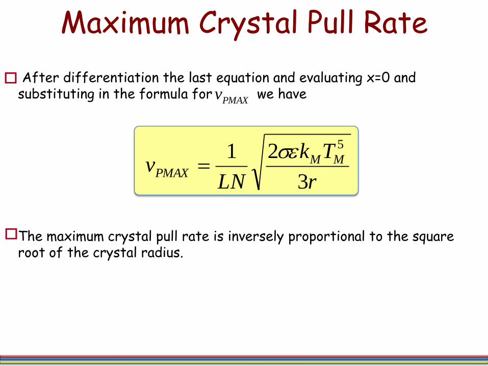
After differentiation the last equation and evaluating x=0 and substituting in the formula for we have
The maximum crystal pull rate is inversely proportional to the square root of the crystal radius.
r
Tk
LNv MM
PMAX3
21 5se
PMAXv
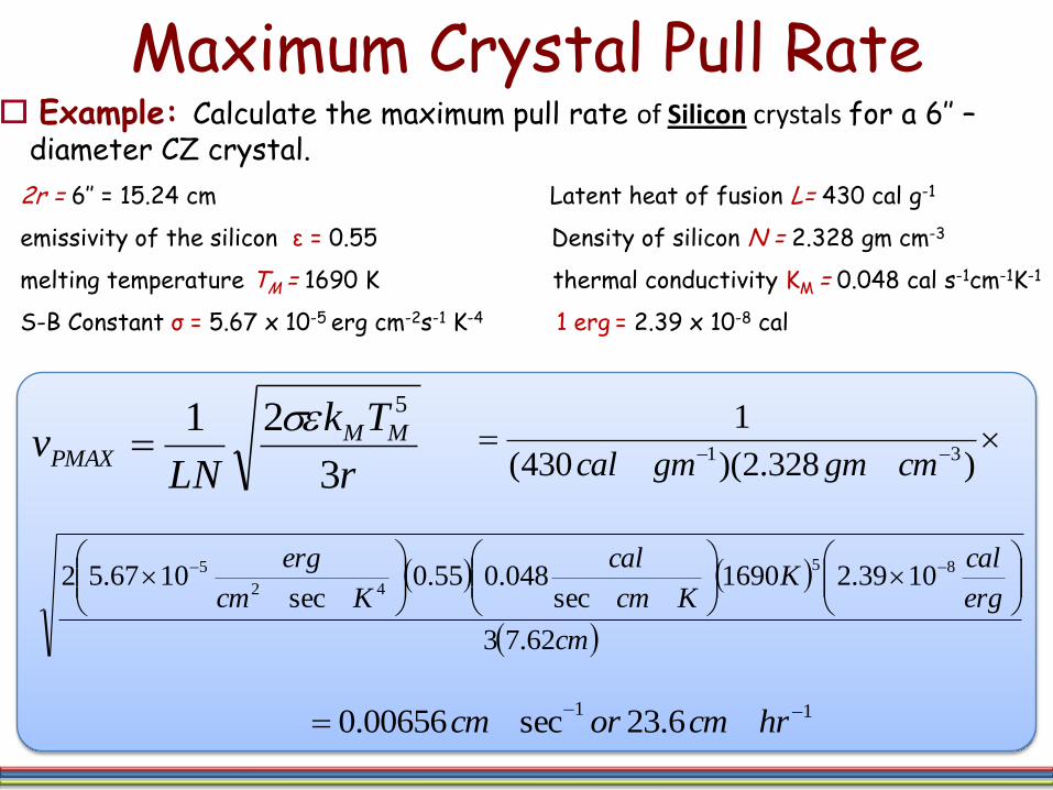
Maximum Crystal Pull RateExample: Calculate the maximum pull rate of Silicon crystals for a 6’’ –
diameter CZ crystal.
2r = 6’’ = 15.24 cm Latent heat of fusion L= 430 cal g-1
emissivity of the silicon ε = 0.55 Density of silicon N = 2.328 gm cm-3
melting temperature TM = 1690 K thermal conductivity KM = 0.048 cal s-1cm-1K-1
S-B Constant σ = 5.67 x 10⁻⁵ erg cm-2s-1 K-4 1 erg = 2.39 x 10⁻⁸ cal
r
Tk
LNv MM
PMAX3
21 5se
)328.2)(430(
131 cmgmgmcal
116.23sec00656.0
hrcmorcm
cm
erg
calK
Kcm
cal
Kcm
erg
62.73
1039.21690sec
048.055.0sec
1067.52 85
42
5
Related Documents