Welcome message from author
This document is posted to help you gain knowledge. Please leave a comment to let me know what you think about it! Share it to your friends and learn new things together.
Transcript
mtl
Elastic laser light scattering by GaAs surfaces
Valeriy A. Sterligov, Yuri V. Subbota, Yuri M. Shirshov, Lidia P. Pochekaylova,Eugene F. Venger, Raisa V. Konakova, and Igor Yu. Ilyin
Angle-resolved scattering ~ARS! intensities were measured in the backscattering hemisphere for the~1 0 0! and ~1 1 1! faces of GaAs single crystals. Three epitaxial layers were deposited onto the GaAs~1 0 0! single-crystalline wafers. The laser elastic light scattering shows the presence of a regularsurface microrelief whose orientation corresponds to the crystallographic axes in the surface plane. Westudied the statistical properties of this microrelief and determined the parameters that characterize thesurface. We propose to use the ARS ratio for two wavelengths ~in our case, 632.8 and 441.6 nm! todetermine the topographical properties of scattering and to study crystal surface defects. © 1999Optical Society of America
OCIS codes: 290.5820, 120.6660, 290.5820, 290.5870, 290.5880, 240.0240.
l
dtscjlsii
wpwamscB
1. Introduction
Elastic light scattering has been used for many yearsto evaluate the quality of polished surfaces.1,2
Among numerous examples of these applications wecan mention the monitoring of crystal structure re-laxation in molecular films by studying the change inangle-resolved light scattering ~ARS! with time.3 Atpresent, elastic light scattering is used for in situ
onitoring of molecular-beam epitaxy growth, oxida-ion, and structural relaxation of III–V crystalayers.4–9 The results of elastic light-scattering
measurements were used in the research reported inRef. 4 to find growth conditions that lead to surfacereconstruction. The authors of Ref. 4 also claimedthat elastic light scattering is more sensitive to sur-face morphology changes than high-energy electrondiffraction, which they also used. The authors ofRefs. 5–8 reported using sample rotation during filmgrowth to measure the azimuthal dependence of thescattered light intensity, using a fixed photodetector.The analysis of these data enabled the authors ofRefs. 5 and 6 to draw some conclusions concerningthe changes in surface topography that one can ob-tain by varying the composition of the growing film.
The authors are with the Institute of Semiconductor Physics,National Academy of Sciences of Ukraine, Prospect Nauki 45,252650 Kiev 28, Ukraine. The e-mail address for V. A. Sterligovis [email protected].
Received 9 April 1998; revised manuscript received 15 October1998.
0003-6935y99y122666-11$15.00y0© 1999 Optical Society of America
2666 APPLIED OPTICS y Vol. 38, No. 12 y 20 April 1999
For films grown upon GaAs ~1 0 0! wafers, a corre-ation was found8 between the light-scattering inten-
sity and the density of a-type misfit dislocations@where the linear-type dislocations were orientedalong the ~0 1 1# ! direction#. The dislocation densitywas found by transmission electron microscopy.The threshold sensitivity for the dislocation densitywas 104 cm22. A light-scattering signal caused byb-type misfit dislocations @oriented along the ~0 1 1!
irection# was also observed. From the optical scat-ering, a critical value for the film thickness of theemiconductor was found. For thicknesses that ex-eeded this value, the misfit dislocation densityumped drastically. The authors of Ref. 8 consideredight-scattering measurements a useful tool for ob-erving both stress relaxation and dislocation growthn the near-surface region of a crystal as well as forllustrating the mechanisms of film growth.
In the research cited above, the ARS dependenceas measured either in the azimuthal plane or in theolar plane. When measurements of the distributionithin the total backscattering hemisphere are made,dditional valuable information is obtained, whichakes it possible to characterize complicated surface
tructure in more detail. Such a method could bealled hemispheric elastic light scattering ~HELS!.y use of HELS,10 information was obtained about the
atomic structure of Si single-crystal surfaces of differ-ent crystallographic orientations. In this paper wepresent the results of HELS measurements made attwo wavelengths ~632.8 and 441.6 nm! on single-crystal GaAs wafers of ~1 0 0! and ~1 1 1! orientations;the ~1 0 0!-oriented wafers were covered with threeepitaxial surface layers. These measurements en-
r
d
fp
2 2 1y2
k
1
abled us to determine the rms roughness of the surfaceand well as its autocorrelation length.
The objectives of our investigation were to study thesurface topography of GaAs crystal surfaces by use ofARS and scattering maps and to use ARS to studysubsurface crystal defects. The results of our studyare important because they demonstrate that one canfind new features of the elastic interaction betweenlight and a crystal by measuring at more than onewavelength. The surface conditions affect the param-eters of GaAs-based field effect transistors and micro-wave integrated circuits that have low noise factors.The presence of point defects and bulk dislocations, aswell as the epilayer surface roughness, results inchanges in many parameters of GaAs wafers, such assurface11 and bulk12 conductivity, Hall mobility,12 fieldeffect transistor threshold voltage,13 leakage cur-ent,12,14 and drain-to-source saturation current.15
2. Theory
A. Vector Scattering Theory
Using the experimental arrangement described inSubsection 3.C, we measured the scattered-light in-tensity Is as a function of azimuthal angle w and polarangle u. We normalized the results to incident lightintensity I0 and photodetector aperture solid angledVs ~Ref. 1! to obtain the bidirectional reflectancedistribution function ~BRDF!:
BRDF~u, w! 51
I0 cos u
dIs
dVs. (1)
The total integrated scattering ~TIS! was calculatedfrom the following relation ~see, for example, Ref. 1!:
TIS 51R * dIs
dVsdVs, (2)
where R is the reflection coefficient.The experimental results were obtained for u $ 4°.
To obtain the missing values for u 5 0° and u 5 2° weused extrapolation, assuming that dIsydu is constantin this region. The rms surface roughness d wascalculated from the TIS value from the relation d 5~ly4p!=TIS, where l is the wavelength of the inci-
ent and scattered light.To characterize the statistical properties of the sur-
ace scattering we calculated the dependence of theower spectral density ~PSD!, g~k! as a function of
wave vector k of the scattered light from the measureddata. According to vector scattering theory,16,17 g~k!is given by g~k! 5 BRDF ~u, w!yOF. Here OF is anoptical factor that depends on the relative permittivityof the material ε, the parameters of the incident light,and the scattering angle. In the case of linearly po-larized, normally incident light, the OF is given by18
OF 5~vyc!4
p2 cos2 uu1 2 εu2
u1 1 Îεu2 Fuq9u2 cos2 w
uq9 1 qεu2
1~vyc!2 sin2 w
uq 1 q9u2 G , (3)
where q 5 ~vyc! cos u, q9 5 @ε~vyc! 2 k # ,5 ~vyc! sin u, and v is the frequency. We used
ε 5 25.869 1 10.250i ~l 5 441.6 nm! and ε 5 14.907 1.5115i ~l 5 632.8 nm! for GaAs. These are litera-
ture values for GaAs, as obtained from Ref. 19. Fi-nally, we used g~k! to determine the autocorrelationfunction for the surface microrelief.1,2,6
B. Surface Statistics
Measured values of PSD g~k! from Subsection 2.Acan often be represented by one of the following mod-els:
Exponential20: g~k! 52pd2s2
@1 1 ~ukus!2#3y2 , (4)
Gaussian20: g~k! 5 pd2s2 exp@2(ukusy2!2#, (5)
ABC model21: g~k! 5A
F1 1 S B2p
ukuD2GCy2 , (6)
In Eqs. ~4! and ~5!, s is the autocorrelation length ofthe surface topography; in Eq. ~6!, parameters A, B,and C are constants. The parameters of the modelfunctions were found by least-squares fitting of themeasured data.
Additional information about the statistical prop-erties of surfaces can thus be obtained from studies ofboth the autocovariance function ~ACF! and the au-tocorrelation function @ACFyACF~0!# as well as fromthe autocorrelation length.
C. Topographic and Nontopographic Scattering
Scattering is defined here to be topographic if thelight is scattered mainly from the sample surface.The contribution from bulk scattering is then as-sumed to be negligible; if such is not the case, one canobserve effects from light interacting with the sub-surface features. These effects may result fromvariations in crystal permittivity caused by the pres-ence of subsurface structural defects, stresses, orother features such as precipitates.
To clarify the scattering mechanism it is useful tocompare the ARS measured at two wavelengths.22
For purely topographic scattering ~light is assumed tobe scattered by a sinusoidal diffraction grating ofamplitude h! the ratio between the diffracted beamintensities measured at two wavelengths has, in theRayleigh approximation, the value
G~h! 5I1~lBLUE!
I1~lRED!5
RBLUE
RRED 3J1S2ph cos ui
lBLUED
J1S2ph cos ui
lREDD4
2
, (7a)
20 April 1999 y Vol. 38, No. 12 y APPLIED OPTICS 2667
u
tfi
tcaTftTon
t2
sh
2
where J1~w! is a Bessel function of the first kind andi is the angle of incidence. For normal incidence,
G~h! 5 const3J1S 2phlBLUE
DJ1S2ph
lREDD 4
2
. (7b)
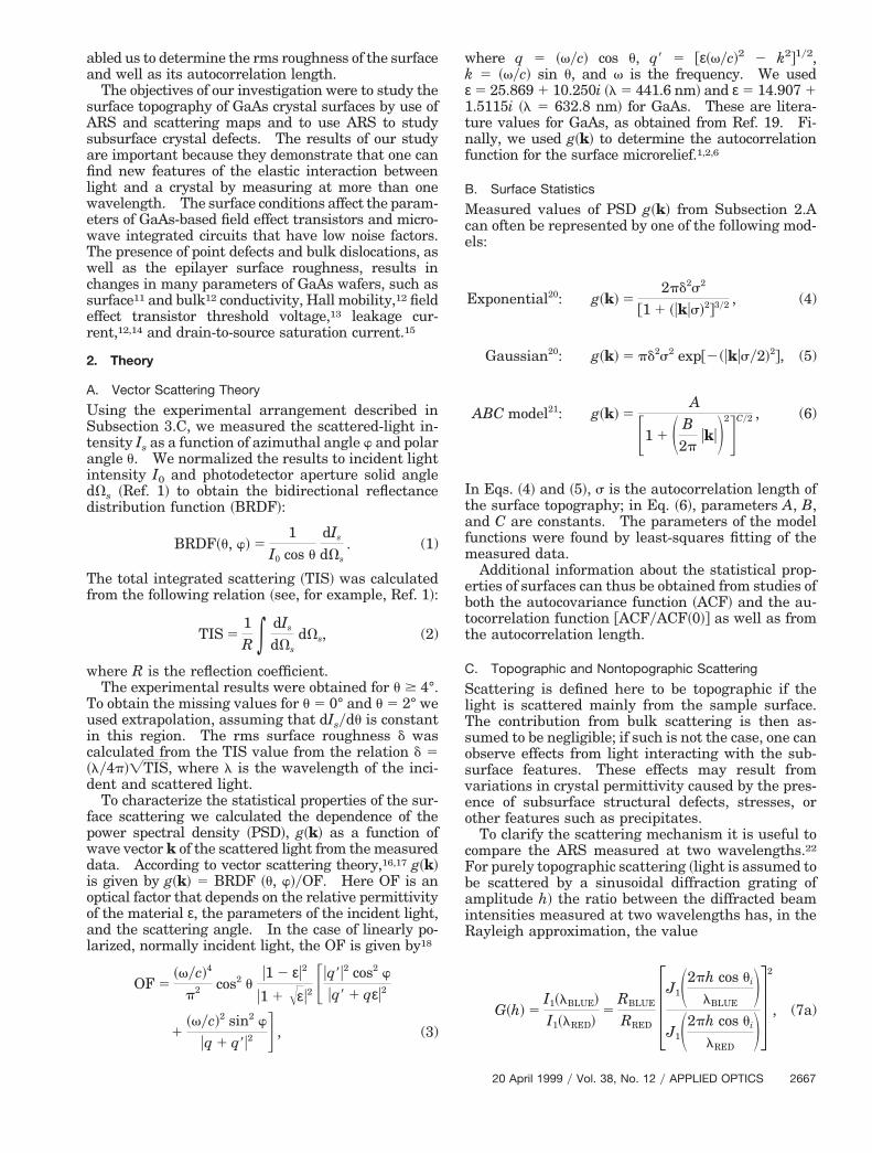
The above ratio is, apart from a constant multipli-cative factor, shown in Fig. 1. One can see that G~h!is independent of h for h values that are #30 nm.Thus, for purely topographic scattering, the ratio be-tween the normalized intensities of light scattered atangles that correspond to the same spatial frequencyf 5 sin uyl remains constant ~up to 30–100 nm!. Ifthis ratio is not constant, the roughness amplitudeexceeds the cited values, the scattering is nontopo-graphic, or both. It should be noted that the aboverange may change when the G~h! dependence is cal-culated exactly.
Real sample surfaces can be represented as a con-tinuous set of diffraction gratings2 that have differentamplitudes, phases, and orientation. For each ofthese gratings one could calculate the value of G byusing the ratio of BRDF values measured for light oftwo wavelengths with the same angle of incidence butfor different directions of scattering that correspondto the same value of spatial frequency. The depen-dence of these ratios on the spatial frequency ~or onthe angle of scattering! will show us how the topo-graphic scattering properties change, so it is reason-able to call this dependence the topographic factor~TF!:
TF~u, w! 5BRDFBLUE~uBLUE, w!
BRDFRED~u, w!,
uBLUE 5 arcsinSlBLUE
lREDsin uD. (8)
The data from TF maps give us information aboutdirections, intensity, and spatial-frequency content of
Fig. 1. Ratio G~h! between the first-order diffraction beam inten-ities for wavelengths of 441.6 and 632.8 nm versus the amplitudeof the sinusoidal relief diffraction grating.
668 APPLIED OPTICS y Vol. 38, No. 12 y 20 April 1999
structures that produce nontopographic scattering.The nontopographic scattering is given by the devia-tion from the calculated values of the TF.
3. Experiment
A. Samples
1. GaAs ~1 1 1! SurfacesWe studied two n-type GaAs wafers oriented alonghe ~1 1 1! direction. The deviation of the surfacesrom this direction was 4 min. The wafers were pol-shed on both sides with the traditional23 polishing
process. The wafer parameters were as follows: di-ameter, 30 mm; thickness, 0.55 6 0.02 mm; charge-carrier concentration, 1–2.6 3 1017 cm23; carriermobility, 3900 cm2yVs. The dislocation density wasin the range 9 3 103 to 1.4 3 104 cm22. The ingotfrom which the wafers were made was doped with Sn.
2. GaAs ~1 0 0! SurfacesWe studied two batches ~20 wafers! of typical indus-trial series-produced GaAs structures. They weremade of alternating sequences of n1–n–n2 epilayersformed by metal-organic vapor–deposited hydrideepitaxy upon semi-insulating GaAs substrates~which are used in manufacturing field-effect transis-tors and microwave integrated circuits that have lownoise factors!. GaAs Czochralski-grown semi-insulating single-crystal ingots doped with Si wereused as host materials for the first batch. GaAsCzochralski-grown, semi-insulating undoped single-crystal ingots were used for the second batch. Thewafers were 60 mm in diameter. The deviation ofthe surfaces from the ~1 0 0! orientation was 3.0° ~0.5°oward the base shear!; the base shear surface coin-ided with that of ~0 1 1! type. The allowable devi-tion of the base shear line was no more than 1°.he dislocation density was less than 105 cm22. Be-
ore building up the epitaxial structure, we treatedhe wafers in a standard sulfuric-acid etchant.hen a sequence of layers was built up by metal-rganic vapor-deposited epitaxy. The first ~buffer!,2, GaAs layer was 1500 nm thick. The charge-
carrier concentration in this layer was 1014 cm23, andhe carrier mobility ~at a temperature of 77 K! was5,000 cm2yVs. The second ~working! layer was of
the n type, and its nominal thickness was 350 nm.The refined values of the thickness and charge-carrier concentration measured for the first batch ofsamples were 338 nm and 1.3 3 1017 cm23, respec-tively. The third ~contact! layer, of the n1 type, was250 nm 6 20% thick, with a charge-carrier concen-tration of 3 3 1018 cm23. The defect concentration ofthe structures corresponded to that of group A ac-cording to the technical specifications.
The surface characteristics of group A must be asfollows: The total length of the scratches and marksshould not exceed 60 mm. The concentration of sur-face defects larger than 300 nm and visible to thenaked eye in fluorescent light should be less than 1cm22. The total area of matte regions and fines ~not
Fwmw
d
H
e
greater than 300 nm and visible to the naked eye!should be less than 0.5 cm2 in spots that are not morethan 2 mm in diameter. We define matte regionsand fines as the surface microrelief or aggregation ofdefects that lead to diffuse scattering of the incidentlight and are clearly visible to the naked eye. Thedislocation density in our structures did not exceed105 cm22. The layers that we studied were suited tothe requirements of GaAs structures with buffer andcontact layers. Because these requirements werenot defined for wafer regions less than 3 mm from theedge, we carried out all the measurements at siteswhose distances exceeded 10 mm from the edge.
B. Maps of Scattered-Light Intensity
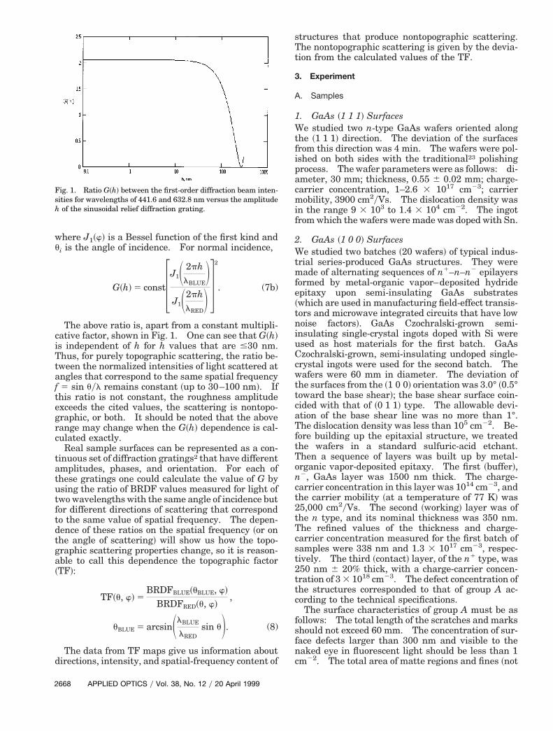
To map the scattered-light intensity from the GaAswafer surfaces we designed a special instrument, ananalyzer of surface defects by laser raster scanning~ADELAR!, a schematic diagram of which is shown in
ig. 2. This is the sixth version of this instrument;e call it ADELAR-6. This instrument was used foreasuring the surface smoothness of semiconductorafers. The beam from a He–Ne laser ~L; wave-
length, 632.8 nm! is reflected by plane mirror M andfocused by an imaging system onto the surface ofsample S. The imaging system consists of a micro-scope objective lens ~MOb, with pinhole D1 at itsfocus! and a beam-expander objective lens ~Ob1!.The cone of light scattered by the sample is focused byobjective lens Ob2 onto diaphragm D2. The cone an-gle, near 60°, and the size of pinhole D2 were fixed.Light passing through D2 is detected by photomulti-plier PM, whose output signal is processed by a com-puter. Scanning of the sample surface isaccomplished by rotation of the sample with steppingmotor SM and translation of stage St, which containsthe sample along a radius. Thus a helical scan pathis obtained. This arrangement allowed us to deter-mine the distribution on the wafer surface of particleswhose effective sizes were more than 300 nm. Theeffective size of a particle is the diameter of a spherethat scatters the same amount of light as the particle.The defects are classified as either point or extended
Fig. 2. Measuring scattered-light-intensity maps. Optical dia-gram of the ADELAR-6 device for monitoring the surface quality.Abbreviations are defined in text.
defects, according to the size of a scattering feature.In the following discussion we consider only extendeddefects, because the vast majority of point defectsresult from surface contamination by either dust orsurface chips and scratches.
A special feature of our optical system is that theincident beam is obliquely incident upon the surface.The ;70° angle of incidence is chosen such that theBrewster angle for the sample lies within the cone oflight focused onto the surface of the sample. Such alayout strongly reduces the specular reflectivity, andthis can increase the ratio between the scattered andthe specularly reflected light intensities.
C. Angle-Resolved Scattering
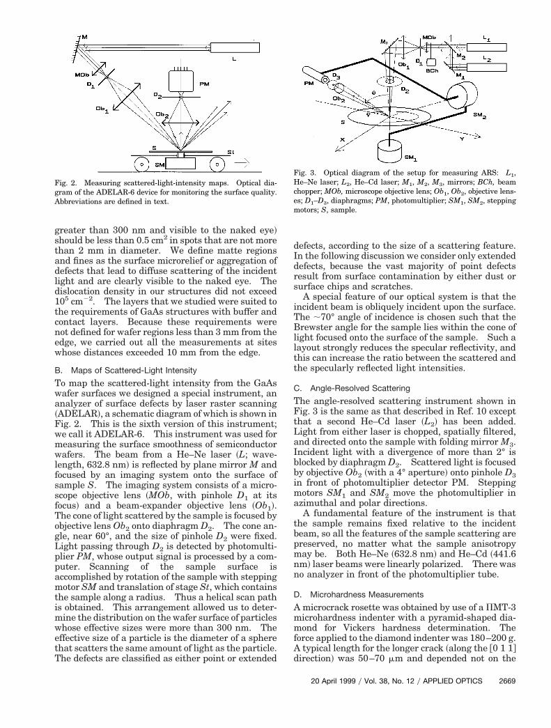
The angle-resolved scattering instrument shown inFig. 3 is the same as that described in Ref. 10 exceptthat a second He–Cd laser ~L2! has been added.Light from either laser is chopped, spatially filtered,and directed onto the sample with folding mirror M3.Incident light with a divergence of more than 2° isblocked by diaphragm D2. Scattered light is focusedby objective Ob2 ~with a 4° aperture! onto pinhole D3in front of photomultiplier detector PM. Steppingmotors SM1 and SM2 move the photomultiplier inazimuthal and polar directions.
A fundamental feature of the instrument is thatthe sample remains fixed relative to the incidentbeam, so all the features of the sample scattering arepreserved, no matter what the sample anisotropymay be. Both He–Ne ~632.8 nm! and He–Cd ~441.6nm! laser beams were linearly polarized. There wasno analyzer in front of the photomultiplier tube.
D. Microhardness Measurements
A microcrack rosette was obtained by use of a PMT-3microhardness indenter with a pyramid-shaped dia-mond for Vickers hardness determination. Theforce applied to the diamond indenter was 180–200 g.A typical length for the longer crack ~along the @0 1 1#
irection! was 50–70 mm and depended not on the
Fig. 3. Optical diagram of the setup for measuring ARS: L1,e–Ne laser; L2, He–Cd laser; M1, M2, M3, mirrors; BCh, beam
chopper; MOb, microscope objective lens; Ob1, Ob2, objective lens-s; D1–D3, diaphragms; PM, photomultiplier; SM1, SM2, stepping
motors; S, sample.
20 April 1999 y Vol. 38, No. 12 y APPLIED OPTICS 2669
a0p
r~ts4mgSfismpm
pstsp
4lsistusprcc
tsatap5
tmot~
Bs
s~
2
orientation of the indenter but on the orientation ofthe crystallographic axes.
4. Results
A. GaAs ~1 1 1! Surfaces
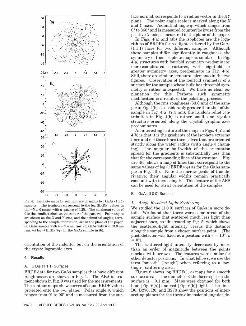
BRDF data for two GaAs samples that have differentroughnesses are shown in Fig. 4. The ARS instru-ment shown in Fig. 3 was used for the measurements.The contour maps show curves of equal BRDF valuesprojected onto the u–w plane. Polar angle u, whichranges from 0° to 90° and is measured from the sur-
Fig. 4. Isophote maps for red light scattering by two GaAs ~1 1 1!samples. The isophotes correspond to the log ~BRDF! values inthe 25 to 0 range, with a spacing of 0.25. The maximum value of0 is the smallest circle at the center of the pattern. Polar anglesare shown on the X and Y axes, and the azimuthal angles, corre-ponding to the sample orientation, are in the plane of the paper.a! GaAs sample with d 5 7.4 nm rms; ~b! GaAs with d 5 53.8 nm
rms, ~c! log ~] BRDFy]w! for the GaAs sample in ~b!.
670 APPLIED OPTICS y Vol. 38, No. 12 y 20 April 1999
face normal, corresponds to a radius vector in the XYplane. The polar angle scale is marked along the Xnd Y axes. Azimuthal angle w, which ranges from° to 360° and is measured counterclockwise from theositive X axis, is measured in the plane of the paper.In Figs. 4~a! and 4~b! the isophotes are the loga-
ithms of BRDF’s for red light scattered by the GaAs1 1 1! faces for two different samples. Althoughhese samples differ significantly in roughness, theymmetry of their isophote maps is similar. In Fig.~a! structures with fourfold symmetry predominate;ore-complicated structures, with eightfold or
reater symmetry axes, predominate in Fig. 4~b!.till, there are similar structural elements in the twogures. Observation of the fourfold symmetry of aurface for the sample whose bulk has threefold sym-etry is rather unexpected. We have no clear ex-
lanation for this. Perhaps such symmetryodification is a result of the polishing process.Although the rms roughness ~53.8 nm! of the sam-
le in Fig. 4~b! is considerably greater than that of theample in Fig. 4~a! ~7.4 nm!, the random relief con-ribution in Fig. 4~b! is rather small, and regulartructure oriented along the crystallographic axesredominates.An interesting feature of the maps in Figs. 4~a! and
~b! is that it is the gradients of the isophote extremaines and not those lines themselves that are orientedtrictly along the wafer radius ~with angle u chang-ng!. The angular half-width of the orientationpread for the gradients is substantially less thanhat for the corresponding lines of the extrema. Fig-re 4~c! shows a map of lines that correspond to theame values of log ~] BRDFy]w! as for the GaAs sam-le in Fig. 4~b!. Note the narrow peaks of this de-ivative; their angular widths remain practicallyonstant with increasing u. This feature of the ARSan be used for strict orientation of the samples.
B. GaAs ~I 0 0! Surfaces
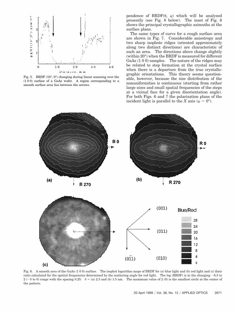
1. Angle-Resolved Light ScatteringWe studied the ~1 0 0! surfaces of GaAs in more de-ail. We found that there were some areas of theample surface that scattered much less light thandjacent ones, as illustrated by Fig. 5, which showshe scattered-light intensity versus the distancelong the sample from a chosen surface point. ~Thehotodetector was fixed at a position with u 5 10°, w
0°!.The scattered-light intensity decreases by more
han an order of magnitude between the pointsarked with arrows. The features were similar for
ther detector positions. In what follows, we use theerm “smooth” ~“rough”! when referring to a low-high-! scattering area.
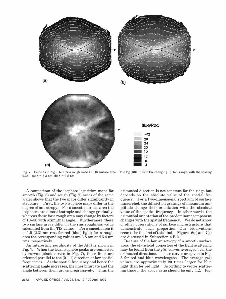
Figure 6 shows log BRDF~u, w! maps for a smoothsurface area. The diameter of the laser spot on thesurface is ;0.1 mm. Maps were obtained for bothblue @Fig. 6~a!# and red @Fig. 6~b!# light. The lines
0, B270, R0, and R270 show the positions of inter-ecting planes for the three-dimensional angular de-
as~GbwganlaFi
pendence of BRDF~u, w! which will be analyzedpresently ~see Fig. 8 below!. The inset of Fig. 6shows the principal crystallographic azimuths at thesurface plane.
The same types of curve for a rough surface areaare shown in Fig. 7. Considerable anisotropy andtwo sharp isophote ridges ~oriented approximatelylong two distinct directions! are characteristic ofuch an area. The directions above change slightlywithin 20°! when the BRDF is measured for differentaAs ~1 0 0! samples. The nature of the ridges maye related to step formation at the crystal surfacehen there is a departure from the true crystallo-raphic orientations. This theory seems question-ble, however, because the size distribution of theonuniformities is continuous ~starting from rather
arge sizes and small spatial frequencies of the stepst a vicinal face for a given disorientation angle!.or both Figs. 6 and 7 the polarization plane of the
ncident light is parallel to the X axis ~w 5 0°!.
thm maps of BRDF for ~a! blue light and ~b! red light and ~c! theirg angle for red light. The log ~BRDF! is in the changing 26.5 toThe maximum value of 2 ~0! is the smallest circle at the center of
Fig. 5. BRDF ~10°, 0°! changing during linear scanning over the~1 0 0! surface of a GaAs wafer. A region corresponding to asmooth surface area lies between the arrows.
Fig. 6. A smooth area of the GaAs ~1 0 0! surface. The isophot logariratio calculated for the spatial frequencies determined by the scatterin2 ~25 to 0! range with the spacing 0.25: d 5 ~a! 2.3 and ~b! 1.5 nm.the pattern.
20 April 1999 y Vol. 38, No. 12 y APPLIED OPTICS 2671
2
A comparison of the isophote logarithm maps forsmooth ~Fig. 6! and rough ~Fig. 7! areas of the samewafer shows that the two maps differ significantly instructure. First, the two isophote maps differ in thedegree of anisotropy. For a smooth surface area theisophotes are almost isotropic and change gradually,whereas those for a rough area may change by factorsof 10–30 with azimuthal angle. Furthermore, thesetwo surface areas differ in the rms roughness valuecalculated from the TIS values. For a smooth area itis 1.5 ~2.3! nm rms for red ~blue! light; for a rougharea the corresponding values are 3.8 nm and 6.4 nmrms, respectively.
An interesting peculiarity of the ARS is shown inFig. 7. When the local isophote peaks are connectedby curves ~black curves in Fig. 7!, these lines areoriented parallel to the ~0 1 1! direction at low spatialfrequencies. As the spatial frequency and hence thescattering angle increases, the lines bifurcate and theangle between them grows progressively. Thus the
Fig. 7. Same as in Fig. 6 but for a rough GaAs ~1 0 0! surface are0.25. ~a! d 5 6.3 nm, ~b! d 5 3.8 nm.
672 APPLIED OPTICS y Vol. 38, No. 12 y 20 April 1999
azimuthal direction is not constant for the ridge butdepends on the absolute value of the spatial fre-quency. For a two-dimensional spectrum of surfacemicrorelief, the diffraction gratings of maximum am-plitude change their orientation with the absolutevalue of the spatial frequency. In other words, theazimuthal orientation of the predominant componentchanges with the spatial frequency. We do not knowof other observations of surface microstructure thatdemonstrate such properties. Our observationsseem to be the first of this kind. Figures 6~c! and 7~c!are discussed in Subsection 4.B.2.
Because of the low anisotropy of a smooth surfacearea, the statistical properties of the light scatteringmay be found from the g~k! curves averaged over theazimuthal directions. These curves are given in Fig.8 for red and blue wavelengths. The average g~k!values are approximately 20 times larger for bluelight than for red light. According to vector scatter-ing theory, the above ratio should be only 4.2. Fig-
he log ~BRDF! is in the changing 26 to 2 range, with the spacing
a. T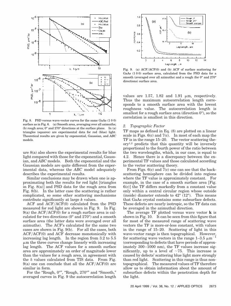
Fcc
To
sd
ure 8~a! also shows the experimental results for bluelight compared with those for the exponential, Gauss-ian, and ABC models. Both the exponential and theGaussian models are quite different from the exper-imental data, whereas the ABC model adequatelydescribes the experimental results.
Similar conclusions may be drawn when one is ap-proximating both the results for red light @trianglesin Fig. 8~a!# and PSD data for the rough area from
ig. 8~b!. In the latter case the scattering is ratheromplicated, so some other scattering mechanismsontribute significantly at large k values.
ACF and ACFyACF~0! calculated from the PSDmeasured for red light are shown in Fig. 9. In Fig.9~a! the ACFyACF~0! for a rough surface area is cal-culated for two directions ~0° and 270°! and a smoothsurface area ~the latter data were averaged over allazimuths!. The ACF’s calculated for the same twocases are shown in Fig. 9~b!. For all the cases, bothACFyACF~0! and ACF decrease monotonically withincreasing lag length. In the region from 3.2 to 5.5mm the three curves change linearly with increasinglag length. The ACF values for a smooth surfacearea are approximately an order of magnitude lowerthan the values for a rough area, in agreement withthe d values calculated from TIS data. From Fig.9~a! one can conclude that all the ACFyACF~0! aresimilar in form.
For the “Rough, 0°”, “Rough, 270°” and “Smooth,”averaged curves in Fig. 9 the autocorrelation length
Fig. 8. PSD versus wave-vector curves for the same GaAs ~1 0 0!surface as in Fig. 6. ~a! Smooth area, averaging over all azimuths;~b! rough area; 0° and 270° directions at the surface plane. In ~a!triangles ~squares! are experimental data for red ~blue! light.Theoretical results are given by exponential, Gaussian, and ABCmodels.
values are 1.57, 1.82 and 1.91 mm, respectively.Thus the maximum autocorrelation length corre-sponds to a smooth surface area with the lowestroughness value. The autocorrelation length issmallest for a rough surface area ~direction 0°!, so thecorrelation is smallest in this direction.
2. Topographic FactorTF maps as defined in Eq. ~8! are plotted on a linearscale in Figs. 6~c! and 7~c!. In most of each map the
F is in the range 15–20. The vector scattering the-ry1,2 predicts that this quantity will be inversely
proportional to the fourth power of the ratio betweenthe two wavelengths, which, in our case, is equal to4.2. Hence there is a discrepancy between the ex-perimental TF values and those calculated accordingto the vector scattering theory.
From Figs. 6~c! and 7~c! one can see that the back-scattering hemisphere can be divided into regionswhere the TF value is approximately constant. Forexample, in the case of a smooth surface area @Fig.6~c!# the TF differs markedly from a constant valueonly within a central circular region whose outside~inside! diameter extends to 42° ~12°!. This meansthat GaAs crystal contains some subsurface defects.These defects are nearly isotropic, so the TF data canbe averaged in the azimuthal direction.
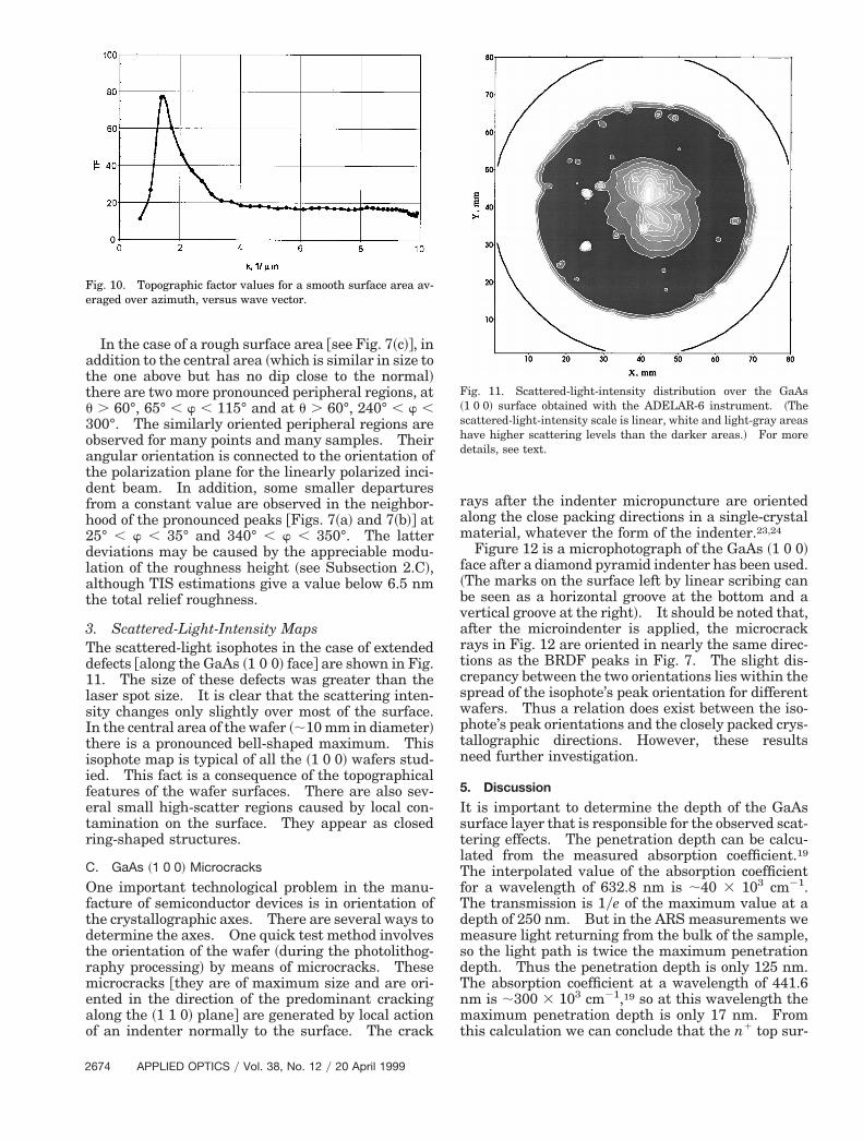
The average TF plotted versus wave vector k isshown in Fig. 10. It can be seen from this figure thatfor most of the measured range of scattering wavevectors the TF is more-or-less constant, with valuesin the range of 15–20. Scattering of light in thiswave-vector range is then topographical. However,for scattering wave vectors in the range 1–3.5 mm21
~corresponding to defects that have periods of approx-imately 300–1000 nm!, the TF values increase sig-nificantly, up to a level of ;75. This increase iscaused by defects’ scattering blue light more stronglythan red light. Scattering in this range is thus non-topographical. The measured values of TF thereforeallow us to obtain information about the amount ofsubsurface defects within the penetration depth forthe light.
Fig. 9. ~a! ACFyACF~0! and ~b! ACF of surface scattering forGaAs ~1 0 0! surface area, calculated from the PSD data for amooth ~averaged over all azimuths! and a rough ~for 0° and 270°irections! surface area.
20 April 1999 y Vol. 38, No. 12 y APPLIED OPTICS 2673
3oatdfh2dlat
3Td1lsItiifetr
eao
f~bvartcswptn
T
2
In the case of a rough surface area @see Fig. 7~c!#, inaddition to the central area ~which is similar in size tothe one above but has no dip close to the normal!there are two more pronounced peripheral regions, atu . 60°, 65° , w , 115° and at u . 60°, 240° , w ,00°. The similarly oriented peripheral regions arebserved for many points and many samples. Theirngular orientation is connected to the orientation ofhe polarization plane for the linearly polarized inci-ent beam. In addition, some smaller departuresrom a constant value are observed in the neighbor-ood of the pronounced peaks @Figs. 7~a! and 7~b!# at5° , w , 35° and 340° , w , 350°. The lattereviations may be caused by the appreciable modu-ation of the roughness height ~see Subsection 2.C!,lthough TIS estimations give a value below 6.5 nmhe total relief roughness.
. Scattered-Light-Intensity Mapshe scattered-light isophotes in the case of extendedefects @along the GaAs ~1 0 0! face# are shown in Fig.1. The size of these defects was greater than theaser spot size. It is clear that the scattering inten-ity changes only slightly over most of the surface.n the central area of the wafer ~;10 mm in diameter!here is a pronounced bell-shaped maximum. Thissophote map is typical of all the ~1 0 0! wafers stud-ed. This fact is a consequence of the topographicaleatures of the wafer surfaces. There are also sev-ral small high-scatter regions caused by local con-amination on the surface. They appear as closeding-shaped structures.
C. GaAs ~1 0 0! Microcracks
One important technological problem in the manu-facture of semiconductor devices is in orientation ofthe crystallographic axes. There are several ways todetermine the axes. One quick test method involvesthe orientation of the wafer ~during the photolithog-raphy processing! by means of microcracks. Thesemicrocracks @they are of maximum size and are ori-nted in the direction of the predominant crackinglong the ~1 1 0! plane# are generated by local actionf an indenter normally to the surface. The crack
Fig. 10. Topographic factor values for a smooth surface area av-eraged over azimuth, versus wave vector.
674 APPLIED OPTICS y Vol. 38, No. 12 y 20 April 1999
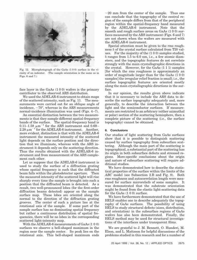
rays after the indenter micropuncture are orientedalong the close packing directions in a single-crystalmaterial, whatever the form of the indenter.23,24
Figure 12 is a microphotograph of the GaAs ~1 0 0!ace after a diamond pyramid indenter has been used.The marks on the surface left by linear scribing cane seen as a horizontal groove at the bottom and aertical groove at the right!. It should be noted that,fter the microindenter is applied, the microcrackays in Fig. 12 are oriented in nearly the same direc-ions as the BRDF peaks in Fig. 7. The slight dis-repancy between the two orientations lies within thepread of the isophote’s peak orientation for differentafers. Thus a relation does exist between the iso-hote’s peak orientations and the closely packed crys-allographic directions. However, these resultseed further investigation.
5. Discussion
It is important to determine the depth of the GaAssurface layer that is responsible for the observed scat-tering effects. The penetration depth can be calcu-lated from the measured absorption coefficient.19
The interpolated value of the absorption coefficientfor a wavelength of 632.8 nm is ;40 3 103 cm21.
he transmission is 1ye of the maximum value at adepth of 250 nm. But in the ARS measurements wemeasure light returning from the bulk of the sample,so the light path is twice the maximum penetrationdepth. Thus the penetration depth is only 125 nm.The absorption coefficient at a wavelength of 441.6nm is ;300 3 103 cm21,19 so at this wavelength themaximum penetration depth is only 17 nm. Fromthis calculation we can conclude that the n1 top sur-
Fig. 11. Scattered-light-intensity distribution over the GaAs~1 0 0! surface obtained with the ADELAR-6 instrument. ~Thescattered-light-intensity scale is linear, white and light-gray areashave higher scattering levels than the darker areas.! For moredetails, see text.
miltsTsm
fat
nudest@ossaf
tsglmoct
HrHawHt
Ep
cF
face layer in the GaAs ~1 0 0! wafers is the primarycontributor to the observed ARS distribution.
We used the ADELAR-6 instrument to obtain mapsof the scattered intensity, such as Fig. 11. The mea-surements were carried out for an oblique angle ofincidence, ;70°, whereas in the ARS measurementsnormal-incidence illumination was used ~Figs. 4–7!.
An essential distinction between the two measure-ments is that they sample different spatial-frequencybands of the surface. The spatial-frequency band is0.11–1.58 mm21 for the ARS instrument and 0.69–2.28 mm21 for the ADELAR-6 instrument. Another,
ore evident, distinction is that with the ADELAR-6nstrument the measured intensity of the scatteredight depends on the surface position and the direc-ion that we illuminate, whereas with the ARS in-trument it depends only on the scattering direction.hus the results obtained with the ADELAR-6 in-trument and from measurement of the ARS comple-ent each other.Let us suppose that the ADELAR-6 instrument is
used to study the surface of a diffraction gratingwhose spatial frequency is such that the diffractedbeam falls within the photodetector aperture. Thenthe measured intensity of the scattered light will risesharply every time the sample is brought into such aposition that the diffracted beam is detected. As aresult, two well-pronounced lobes ~for the first-orderdiffraction beams detected! appear on the samplesurface map. These lobes are oriented along thenormal to the direction of the diffraction gratinggrooves. The center of such a picture lies at therotational axis of the sample. If some part of thesample surface has no dominating spatial frequencybut rather a continuous distribution of spatial fre-quencies, there will be no lobes in the correspondingscattered light-intensity map.
With the ADELAR-6 measurements of GaAs ~1 0 0!surfaces we observe a bell-shaped maximum in theregion near the sample center. Its peak lies on therotational axis. This bell-shaped maximum ends
Fig. 12. Microphotograph of the GaAs ~1 0 0! surface in the vi-inity of an indenter. ~The sample orientation is the same as inigs. 6 and 7.!
;20 mm from the center of the sample. Thus onecan conclude that the topography of the central re-gion of the sample differs from that of the peripheralregion within the spatial-frequency band measuredby the ADELAR-6 instrument. Note that thesmooth and rough surface areas on GaAs ~1 0 0! sur-aces measured by the ARS instrument ~Figs. 6 and 7!re not shown when the wafers are measured withhe ADELAR-6 instrument.
Special attention must be given to the rms rough-ess d of the crystal surface calculated from TIS val-es. For the majority of the ~1 0 0! samples studied,ranges from 1.5 to 6.0 nm, i.e., a few atomic diam-
ters, and the topographic features do not correlatetrongly with the main crystallographic directions inhe crystal. However, for the GaAs ~1 1 1! samplesfor which the rms roughness is approximately anrder of magnitude larger than for the GaAs ~1 0 0!amples# the irregular relief fraction is small; i.e., theurface topographic features are oriented mostlylong the main crystallographic directions in the sur-ace.
In our opinion, the results given above indicatehat it is necessary to include the ARS data to de-cribe the surface topography adequately and, moreenerally, to describe the interaction between theight and the semiconductor surfaces. If measure-
ents are restricted to an arbitrary ~either azimuthalr polar! section of the scattering hemisphere, then aomplete picture of the scattering ~i.e., the surfaceopography! cannot be obtained.
6. Conclusions
Our studies of light scattering from GaAs surfacesshow that it is possible to distinguish scatteringcaused by surface topography from subsurface scat-tering. Although the main part of the scattering istopographical, a substantial part of the scattering hasits origin in both subsurface defects and stressed re-gions. More-specific conclusions about the originand nature of subsurface scattering will require ad-ditional studies.
We have demonstrated how to describe the statis-tical properties of the surface within the limits of theABC model ~see Subsection 2.B and Fig. 8!. Bothrms roughness and autocorrelation length were mea-sured for surface microreliefs of some samples. Itwas demonstrated that the substrate orientationmight be found from the elastic light-scattering datafor the GaAs ~1 0 0! surface.
We have furthermore demonstrated that the use ofELS enables one to describe adequately the topog-
aphy of GaAs surfaces. The possibility of usingELS to study structural defects ~sizes, distribution,nd orientation! in the subsurface regions of GaAsafers has also been demonstrated. Finally, theELS method may be used for structural investiga-
ions of the interfaces under transparent films.
We are grateful to J. M. Bennett, O. Hunderi, M.lson, and L. Mattsson for helpful discussions of theroblems studied in this research and for a number of
20 April 1999 y Vol. 38, No. 12 y APPLIED OPTICS 2675
sistivity, Hall mobility and leakage current variations in un-
2
valuable comments. The research was partiallysupported by grant 06.01.00y002-95 from the StateCommittee for Science and Technologies of Ukraine.
References1. J. M. Bennett and L. Mattsson, Introduction to Surface Rough-
ness and Scattering ~Optical Society of America, Washington,D.C., 1989!.
2. J. C. Stover, Optical Scattering: Measurement and Analysis~SPIE Optical Engineering Press, Bellingham, Wash., 1995!.
3. D. Oelkrug, J. Haiber, R. Lege, H. Stauch, and H.-J. Egelhaaf,“Temporal stability of vapor deposited molecular films as stud-ied by laser light scattering,” in Proceedings of the SeventhInternational Conference on Organized Molecular Films, Nu-mana ~Ancona!, Italy, 10–15 September 1995 ~CINECA, Bolo-gna, 1996!, pp. 173–176.
4. K. Yang, E. Mirabelli, Z.-C. Wu, and L. J. Schowalter, “In situlaser light scattering for monitoring III–V semiconductor filmgrowth by molecular-beam epitaxy,” J. Vac. Sci. Technol. B 11,1011–1013 ~1993!.
5. J. Epler, J. Sochtig, and H. Sigg, “Evolution of surface topog-raphy during metalorganic vapor phase epitaxy of InPyIn-GaAsyInP quantum well heterostructures,” Appl. Phys. Lett.65, 1949–1951 ~1994!.
6. G. W. Smith, A. J. Pidduck, C. R. Whitenhou, J. L. Glasper, andJ. Spowart, “Real time laser light scattering studies of surfacetopography development during GaAs MBE growth,” J. Cryst.Growth 127, 966–972 ~1993!.
7. F. G. Celii, L. A. Filesses, E. A. Beam, and H. Y. Liu, “In situdetection of InGaAs strained layer relaxation by laser lightscattering,” J. Vac. Sci. Technol. A 11, 1796–1802 ~1993!.
8. F. G. Celii, Y. C. Kad, H. Y. Liu, L. A. Filesses, and E. A. Beam,“Laser light scattering detection of InGaAs strained layer re-laxation,” J. Vac. Sci. Technol. B 11, 1014–1017 ~1993!.
9. F. G. Celii, E. A. Beam, H. Y. Liu, and Y. C. Kad, “In situdetection of relaxation in InGaAsyGaAs strained layer super-lattices using laser light scattering,” Appl. Phys. Lett. 62,2705–2707 ~1993!.
10. G. E. Domashev, Yu. M. Shirshov, V. A. Sterligov, Yu. V.Subbota, and S. V. Svechnicov, “Atomic structure display of areal silicon surface under light scattering,” Appl. Opt. 34,2367–2371 ~1995!.
11. R. T. Blunt, S. Clark, and D. J. Stirland, “Dislocation densityand sheet resistance variations across semi-insulating GaAswafers,” IEEE Trans. Electron Devices ED-29, 1039–1045~1982!.
12. T. Matsumura, H. Emori, K. Terashima, and T. Fukuda, “Re-
676 APPLIED OPTICS y Vol. 38, No. 12 y 20 April 1999
doped semi-insulating GaAs crystal grown by LEC method,”Jpn. J. Appl. Phys. 2, Lett. 22, L154–L156 ~1983!.
13. Y. Nanishi, S. Ishida, and T. Honda, eds., “InhomogeneousGaAs FET threshold voltages related to dislocation distribu-tion,” Jpn. J. Appl. Phys. 2, Lett. 21, L335–L337 ~1982!.
14. Y. Matsumoto and H. Watanabe, “Inhomogeneity in semi-insulating GaAs revealed by scanning leakage current mea-surements,” Jpn. J. Appl. Phys. 21, L515–L517 ~1982!.
15. Y. Nanishi, S. Ishida, and S. Miyazawa, “The influence ofdislocation density on the uniformity of electrical properties ofSi implanted, semi-insulating LEC-GaAs,” Jpn. J. Appl. Phys.22, 270–272 ~1983!.
16. J. M. Elson and J. M. Bennett, “Relationship between theangular dependence of scattering and the statistical propertiesof smooth optical surfaces,” J. Opt. Soc. Am. 69, 31–47 ~1979!.
17. J. M. Elson and J. M. Bennett, “Vector scattering theory,” Opt.Eng. 18, 116–124 ~1979!.
18. J. M. Elson, J. P. Rahn, and J. M. Bennett, “Relationship of thetotal integrated scattering from multilayer-coated optics toangle of incidence, polarization, correlation length, and rough-ness cross-correlation properties,” Appl. Opt. 22, 3207–3219~1983!.
19. J. B. Theeten, D. E. Aspnes, and R. P. H. Chang, “A newresonant ellipsometric technique for characterizing the inter-face between GaAs and its plasma-grown oxide,” J. Appl. Phys.49, 6097–6102 ~1978!.
20. J. M. Elson, J. M. Bennett, and J. C. Stover, “Wavelength andangular dependence of light scattering from beryllium: com-parison of theory and experiment,” Appl. Opt. 32, 3362–3376~1993!.
21. E. L. Church and P. Z. Takacs, “The optimal estimation offinish parameters,” in Optical Scatter: Applications, Mea-surement, and Theory, J. C. Stover, ed., Proc. SPIE 1530,71–78 ~1991!.
22. L. Mattsson, J. Ingers, and J. M. Bennett, “Wavelength depen-dence of angle-resolved scattering in the extreme-ultraviolet-visible region,” Appl. Opt. 33, 3523–3532 ~1994!.
23. “Single-crystalline gallium arsenide wafers,” Technical Stan-dard 11-87 (Research and Production Association, ELMA,Moscow, 1987).
24. D. Scannell and D. Smith, “Scribing compound semiconduc-tors: an application primer,” Microelectron. ManufacturingTesting 11, 10–11 ~1988!.
25. O. I. Bochkin, Mechanical Processing of Semiconductor Mate-rials ~Vysshaya Shkola, Moscow, 1983; in Russian!.
Related Documents