MONITORING AND CONTROL OF 3-TIER POWER SUPPLY BY EGBUCHULAM, EKENNA (PG/M.ENG/09/50877) DEPARTMENT OF ELECTRONIC ENGINEERING FACULTY OF ENGINEERING UNIVERSITY ON NIGERIA, NSUKKA AUGUST, 2015

Welcome message from author
This document is posted to help you gain knowledge. Please leave a comment to let me know what you think about it! Share it to your friends and learn new things together.
Transcript
MONITORING AND CONTROL OF 3-TIER POWER SUPPLY
BY
EGBUCHULAM, EKENNA (PG/M.ENG/09/50877)
DEPARTMENT OF ELECTRONIC ENGINEERING FACULTY OF ENGINEERING UNIVERSITY ON NIGERIA,
NSUKKA
AUGUST, 2015
i
TITLE PAGE
MONITORING AND CONTROL OF 3-TIER POWER SUPPLY
BY
EGBUCHULAM, EKENNA (PG/M.ENG/09/50877)
DEPARTMENT OF ELECTRONIC ENGINEERING UNIVERSITY ON NIGERIA, NSUKKA
AUGUST, 2015
ii
APPROVAL PAGE
MONITORING AND CONTROL OF 3-TIER POWER SUPPLY
BY
EGBUCHULAM, EKENNA
(PG/M.ENG/09/50877)
A THESIS SUBMITTED IN PARTIAL FULFILLMENT OF THE REQUIREMENTS FOR THE AWARD OF
MASTER OF ENGINEERING (DIGITAL ELECTRONICS AND COMPUTER OPTION) IN THE
DEPARTMENT OF ELECTRONIC ENGINEERING, UNIVERSITY OF NIGERIA, NSUKKA.
EGBUCHULAM, EKENNA SIGNATURE……………………. Date………………… (STUDENT) PTOF. O. U. OPARAKU SIGNATURE……………………. Date………………… (SUPERVISOR)
EXTERNAL EXAMINER SIGNATURE……………………. Date………………… PROF. C. I. ANI SIGNATURE……………………. Date………………… (HEAD OF DEPARTMENT)
PROF. E. S. OBE SIGNATURE……………………. Date………………… (CHAIRMAN, FACULTY POSTGRADUATE COMMITTEE)
iii
CERTIFICATION
Egbuchulam Ekenna, a Master’s degree postgraduate student in the Department
of Electronic Engineering, University of Nigeria, Nsukka, with registration number
PG/M.ENG/09/50877, has satisfactorily completed the requirements for the
award of a Master of Engineering (M.Eng) in Electronic Engineering.
…………………………………. …………………………………….. PROF. O. U. OPARAKU PROF. C. I. ANI (SUPERVISOR) (HEAD OF DEPARTMENT)
….…….…………………………………….. PROF. C. I. ANI
(CHAIRMAN, FACULTY POSTGRADUATE COMMITTEE )

iv
DECLARATION
I, Egbuchulam Ekenna, a postgraduate student of the Department of Electronic
Engineering, University of Nigeria, Nsukka, declare that the work embodied in this
thesis is original and has not been submitted by me in part or in full for any other
diploma or degree of this University or any other Universities.
………………………………………………… …………………………………….. EGBUCHULAM EKENNA DATE (STUDENT)

v
DEDICATION
I fondly dedicate this work to God Almighty, who made it all happen, and to the
memory of my mum, Mrs. C. B. Egbuchulam, whose concern to see me stand
never failed, till her very last breath.

vi
Acknowledgement
Firstly, I want to give thanks to Almighty God for His sustained guidance, protection and provision throughout the course of this work. This project couldn’t have been completed but for the blessings of God. I wish to appreciate profoundly my supervisor and teacher, Professor O. U. Oparaku, not only for getting me started on this work, but for his endless contribution of ideas and direction all the way through. To Engr. and Engr. Mrs. Kesandu-Uchenyi, who always were a big source of inspiration and motivation, I want to say a big thank you. I also thank and appreciate immensely Engr. V. C. Chijindu, for the useful advice, support and constructive critique he gave during the final stages of this work. I am deeply indebted to my friend and colleague Gabe Akanyak, whose wealth of experience was a useful resource all through this work. My siblings, especially big sister Henn Onuoha, who paid the fees when it mattered most, I thank God for such a blessing as you. And last, but by no means the least, my lovely wife Nkechi, for her understanding and unremitting care while I was on this project.

vii
Abstract
Reliable electricity supply is essential for development. As a result, demand for
electricity has continued to increase globally, occasioned by the fact that
electricity is highly portable and can be transformed from one form to another to
meet needs. In Nigeria and most developing countries, electricity supply from the
public utility is not only insufficient but highly erratic. The effect of this is adverse
on critical and sensitive infrastructure that depend on uninterrupted power
supply. Hence, many domestic, industrial and commercial consumers are
compelled to acquire one form of alternative source of power supply or another.
With this however, when different power schemes are interconnected, there
arises the challenge of switching between the power sources not only smoothly,
but in a manner that optimizes their use. Solving these challenges forms the focus
of this work. This design monitors three independent power sources: Utility Grid
of Power Holding Company of Nigeria (PHCN), solar and generator and engages
them following preset conditions in a microcontroller. A software program in
assembly language drives the microcontroller. Preference is given to the PHCN
line, but in the event of failure or abnormal conditions in the PHCN line, the
system will effect a changeover automatically to the solar source through
contactors, provided the output of the solar source is acceptable, else the system
will initiate the starting of the generator and transfer of load to same. This system
finds application wherever there is unreliable power supply and interconnected
power schemes.

viii
TABLE OF CONTENTS TITLE PAGE i
APPROVAL PAGE ii
CERTIFICATION iii
DECLARATION iv
DEDICATION v
ACKNOWLEDGEMENT vi
ABSTRACT vii
TABLE OF CONTENT viii
CHAPTER ONE INTRODUCTION 1
1.0 Project background 1
1.1 Statement of problem 2
1.2 Project objectives 2
1.3 Significance of project 3
CHAPTER TWO LITERATURE REVIEW 4
2.0 Electricity in Nigeria 4
2.0.1 Nigeria’s Electricity Sector in Retrospect 5
2.0.2 Nigeria’s Power Sector Reform 6 2.0.3 Electricity Power Sector after Privatisation 8 2.0.4 Electricity Production and Consumption in Nigeria 11
2.1 Electricity from Solar 13
2.1.0 Components of a PV system 14
2.1.1 Design Considerations 20
2.1.2 Energy from the PV module 21
2.2 Use of Generators 22
2.3 Transfer Switches 23
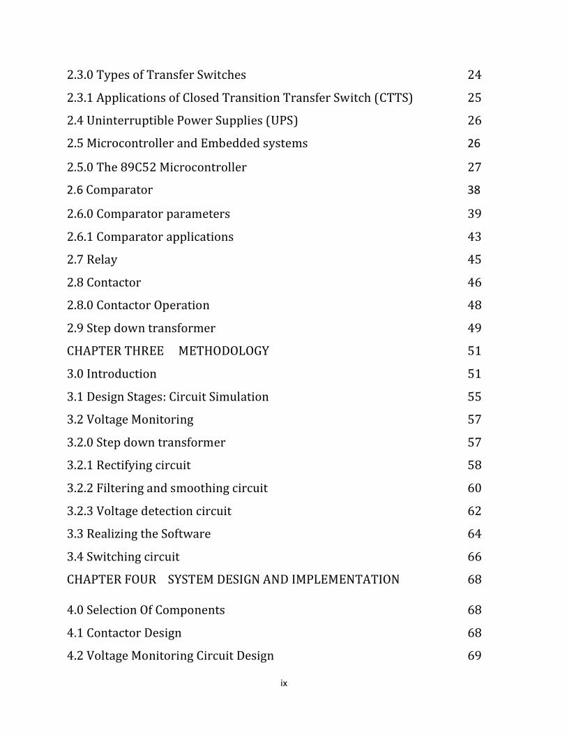
ix
2.3.0 Types of Transfer Switches 24
2.3.1 Applications of Closed Transition Transfer Switch (CTTS) 25
2.4 Uninterruptible Power Supplies (UPS) 26
2.5 Microcontroller and Embedded systems 26
2.5.0 The 89C52 Microcontroller 27
2.6 Comparator 38
2.6.0 Comparator parameters 39
2.6.1 Comparator applications 43
2.7 Relay 45
2.8 Contactor 46
2.8.0 Contactor Operation 48
2.9 Step down transformer 49
CHAPTER THREE METHODOLOGY 51
3.0 Introduction 51
3.1 Design Stages: Circuit Simulation 55
3.2 Voltage Monitoring 57
3.2.0 Step down transformer 57
3.2.1 Rectifying circuit 58
3.2.2 Filtering and smoothing circuit 60
3.2.3 Voltage detection circuit 62
3.3 Realizing the Software 64
3.4 Switching circuit 66
CHAPTER FOUR SYSTEM DESIGN AND IMPLEMENTATION 68
4.0 Selection Of Components 68
4.1 Contactor Design 68
4.2 Voltage Monitoring Circuit Design 69

x
4.3 Circuit Breaker Design 72
4.4 Relay Design 73
4.5 Pilot and Indication Lamps 73
4.6 Conductor Design 73
4.7 Testing and results 74
4.8 Cost analysis 76
CHAPTER FIVE CONCLUSION AND RECOMMENDATION 78
5.0 Conclusion 78
5.1 Recommendation 78
REFERENCES 79
APPENDIX A 83
APPENDIX B 86
APPENDIX C 91
APPENDIX D 103

1
CHAPTER ONE
INTRODUCTION 1.0 Project Background
Electricity is of enormous importance to the society today. It is indispensable to
social and economic development. Modern industrial systems depend on regular
supply of electricity. Quality of life and standard of living today depend much on
electricity. People need energy in one form or the other (heat, light, sound etc)
and electricity is most convenient in that it can be converted with ease from one
form to another.
However, in many developing nations steady availability of electricity is yet to be
realized. In Nigeria, for instance, the supply of electricity from the public utility
(PHCN) is unreliable, marked by incessant outages, and therefore inadequate for
any meaningful advancement in industrial, commercial and domestic activities.
Generators are commonly used in Nigeria but the cost of running diesel or other
fuel for running generators all the time is not feasible for both home and business
concerns. Renewable sources like solar are also used but so far there is yet room
for improvement before solar power can be utilized without some form of
backup. Thus, multi-tier power supply, a system of more than one power source,
has gradually become the norm in our society.
This project “Monitoring and Control of 3-tier Power Supply” provides a way of
monitoring and switching between three different power sources in order to
optimize their use.
2
1.1 Statement of Problem
The demand for energy especially electrical energy is on the increase globally and
power utilities strive to match supply with demand. A lot of large-scale industrial
critical loads suffer from voltage interruptions and sags which can cause a
significant financial loss [1]. In Nigeria the actual generating capacity falls short of
the installed capacity and the country’s peak demand due to problems in the
power systems network [2]. The country requires over 6000 MW of electricity to
meet present demand. Current output is around 3000MW, much of which is not
put to use due to poor power transmission and distribution infrastructure [3]. The
effect is that supply from the national grid has been very low and unsteady over
the years with the result that people have resorted to integrating multiple power
sources as a remedial measure.
The problem is the need to monitor these power sources and switch between
them in a manner that ensures safety of personnel and equipment. There is also a
need to optimize their use by setting the preferred power source as default
through some device.
1.2 Project Objectives
The objectives of this project include:
1. To monitor and control a three tier power supply system.
2. To automate the power changeover process to ensure a smooth transfer of
load for the purpose of safety and convenience.
3. To implement a system of power change over with minimal time wastage.
4. To optimize power use in a system of 3 power sources by setting the most
economical power source as default in the system.

3
1.3 Significance of the Project
Electricity which is an essential tool to development and indeed civilization is a
necessity that should be readily available. As stated earlier the demand for
electricity is on the increase globally. However, the shortfall in supply from the
national grid creates a need which this project seeks to fill.
This project is significant because it seeks to provide a cost effective way of using
multitier power supplies which are common in developing societies like Nigeria. In
addition, it ensures a smooth and safe means of power changeover during
outages through an automated process.
Further it is expected that this work will benefit power system managers, public
policy analysts, policy makers, scholars and the general public.

4
CHAPTER TWO
LITERATURE REVIEW
2.0 Electricity in Nigeria
Electricity generation in Nigeria started in 1896 although it was not until 1929 that
the first utility company, the Nigerian Electricity Supply Company was established
[4].
In the 1950s and 1960s the Nigerian government created the Electricity
Corporation of Nigeria to control all existing diesel/coal fired isolated power
plants across the country and the Niger Dams Authority to develop hydroelectric
power in Nigeria. These two entities were amalgamated into the National Electric
Power Authority (NEPA) in 1972, and in 2004, the need to reform the Electricity
industry necessitated the transformation of NEPA into Power Holding Company of
Nigeria (PHCN).
Electricity generation, transmission and distribution in Nigeria account for less
than one per cent of the Gross Domestic Products (GDP) [5]. Until the recent
unbundling and handover of PHCN to successor companies, PHCN dominated
Nigeria’s electricity sector, supplying most of the electricity consumed in Nigeria,
supplemented with power generated from privately-owned plants. There is still a
high incidence of privately-owned plants usually referred to as ‘captive power
plants’. This in most cases is in response to irregular public power generation and
transmission.

5
2.0.1 Nigeria’s Electricity Sector in Retrospect
Electric Power development in Nigeria started toward the end of 19th century
when the first generating plant of 30KW was installed in the city of Lagos in 1898
[6]. From this date onwards and until 1950, the pattern of electricity development
was in form of individual electricity undertaking set up in various towns
somewhere by Native or Municipal authorities.
In 1946, the Nigerian Government Electricity undertaking was established within
the then Public Works Department (PWD) to take over the responsibility for
electricity in Lagos State.
In 1950 the Government passed the Electricity Corporation of Nigeria Ordinance
No.1 of 1950 to integrate power development and make it effective. This
ordinance brought all the electricity undertakings and the electricity sections of
PWD under control. The Electricity Corporation of Nigeria (ECN) then became the
statutory body responsible for Generation, Transmission, Distribution and Sales of
Electricity to all consumers in Nigeria.
In 1962, the Niger Dams Authority was established by an Act of the Parliament.
The Authority was responsible for the construction and maintenance of Dams and
other works on the river Niger and elsewhere, generating electricity by means of
water, improving navigation and promoting fisheries and irrigation.
The Electricity Corporation of Nigeria (ECN) and the Niger Dams Authority (NDA)
were merged to become National Electric Power Authority (NEPA) by decree
No.24 of 1972. The Authority was to develop, maintain and co-ordinate an
efficient economic system of electricity supply for all parts of the Federation. The

6
Authority generates electricity through two major sources: Hydro and Thermal.
The Hydro Power stations are Kainji Hydro Power station with capacity of
760MW, Jebba Hydro Power station with 578.4MW capacity, Shiroro Hydro
Power Station 600MW. The Thermal Power stations are: Afam Thermal Power
station with 696MW, Lagos thermal power station, Delta IV thermal Power
station with 600MW and Sapele Thermal Power station 1020MW. The existing
power stations in Nigeria are shown in appendix A.
However, the need to reform the Electricity industry necessitated the
transformation of NEPA into Power Holding Company of Nigeria (PHCN) in 2004.
Today, non-availability of spare parts and poor maintenance have been identified
as major problems of PHCN. Also, a poorly-motivated workforce, vandalisation,
theft of cables and other vital equipment, accidental destruction of distribution
lines, illegal connections and resultant over-loading of distribution lines, are
additional major problems of the sector. These have been responsible for
unannounced load shedding, prolonged and intermittent outages which most
consumers of electricity in Nigeria have had to contend with over the years. It is
apparent that the poor performance of the electricity power sector in Nigeria
since inception has been a significant obstacle preventing private investment, the
overall development and economic growth in the country [7].
The Electricity Reform Act of 2005, unbundled PHCN into 11 Distribution
companies, 1 Transmission Company and 6 Generation companies.
2.0.2 Nigeria’s Power sector Reform
Through the Electric Power Sector Act of 2005 (EPSA 2005), the Federal
Government began the unbundling of the power industry for the eventual

7
deregulation and privatisation of the power generation and distribution in Nigeria
in a bid to make it more efficient in meeting existing and prospective
consumption demand [8]. As a result, the Power Holding Company of Nigeria
(PHCN) was established with an intended strategy to privatise core functions of
the power company such as generation and distribution, whilst transmission
operations would be retained by the government.
Prior to the enactment of the Electricity Power Sector Reform Act (EPSRA), 2005,
the Federal Government was responsible for policy formulation, regulation,
operation, and investment in the Nigerian power sector. However, EPSRA Act
became law in 2005, providing legal backing to the power sector reform
programme, leading to the launch of the Power Sector Roadmap by President
Goodluck Jonathan in August 2010 [9].
In order to attract private sector investment and sustain the development of the
power sector to ensure uninterrupted and efficient power supply in the country,
the National Council on Privatization (NCP) defined the objectives for power
sector reform as follows.
1. To promote competition and facilitate more rapid provision of service
throughout the country;
2. To create a new legal and regulatory environment for the sector that
establishes a level playing field, encourages private investment and expertise,

8
and meets social goals;
3. To restructure and privatize the National Electric Power Authority (NEPA); and,
4. To encourage the successors to NEPA to undertake an ambitious investment
program [10].
On November 1, 2013, the assets of Power Holding Company of Nigeria (PHCN)
were physically handed over to their new owners. The Nigerian Electricity
Regulatory Commission (NERC) and the Bureau of Public Enterprises (BPE) were
saddled with the responsibility to monitor the operations of the successor
companies. Currently, NERC is facing challenges in addressing the near failure in
generation as a result of acute shortage in gas supply to most of the thermal
stations. Similarly, the NERC also appears not to have panacea to estimated
billing, one of the issues that have pitched consumers against the distribution
companies. Indeed, the Commission is at crossroads dealing with high ineptitude
in the value chain [11].
2.0.3 Electricity Power Sector after Privatization
The privatization exercise involved the sale of eleven distribution companies
(DISCOS), seven generation companies (GENCOS) and the appointment of
Manitoba Hydro International of Canada to manage the Transmission Company of
Nigeria (TCN).
There has been a period for teething problems, more so as some of the
generation companies, such as Afam, Kaduna and Sapele experienced late
completion of their privatisation. It is expected that it would take some time
before the new private operators would fully take over and begin to make the
much expected difference [12].

9
Meanwhile, the power supply has fallen, while many consumers from across the
country are groaning over new “crazy” bills which no one appears to be available
to explain the rationale for them.
The operational methods of the new owners and operators of the nation’s power
system is quite different from what took place in the telecoms sector, where
competition, promos and avalanches of public enlightenment invaded the media.
Private operation of telecoms took a life of its own from the onset and
established a bridge to the public that helped shape the industry to esteemed
position it has attained today.
The enormous challenges of weak electricity transmission network and low
generation capacity inherited from the defunct government-owned Power
Holding Company of Nigeria (PHCN) is putting the brakes on the investment drive
of new owners of the distribution companies (Discos) [13].
The Discos which are the closest to the customers on the electricity value chain,
have been grappling with revenue collection from customers since the take-over
late last year, when power supply in many parts of the country declined.
Some of the Discos that have already invested in upgrading their power assets, it
was gathered, are now very wary of making further investments pending when
transmission and generation capacities would increase [14].
Also, some of the generation companies (Gencos) which were planning to
increase capacity are being constrained by gas supply shortages. Generation,
which peaked at 4,517 megawatts (MW) in December 2012, is now hovering
between 3,000MW and 3,500MW, no thanks to gas supply shortages.
10
Added to this problem is the issue of revenue collection which would require that
strategies be put in place to optimise. Capacity expansion will be gradual and will
remain subject to considerable risks and delays. While significant demand for
electricity undoubtedly exists, disputes over tariffs, gas shortages and concerns
about the country’s business environment could all weigh on investment.
The challenge of gas supply to power plants and system collapse have continued
to limit generation capacity, with massive investment required to upgrade
dilapidated power generation and transmission facilities, some of which have
become problematic due to their age and years of neglect. There is need for the
new investors to drive the government to do its part particularly in the areas of
gas supplies and transmission. Power that does not reach the consumers does not
translate to money.
Beyond revenue collection, the market is still very unstable. Generation capacity
has not radically improved. Nigeria’s daily electricity generation capacity is
currently fluctuating between 4,400 and 4,500 megawatts [15], and the
transmission network is also weak. Even if generation improves, the transmission
network is not strong enough to evacuate generated power. There is an urgent
need to expand the transmission network.
In what is an acknowledgement of the need to expand the transmission capacity,
the Federal Government in its 2014 budget proposal allocated about N25 billion
to the Transmission Company of Nigeria (TCN), out of the N62 billion to the power
sector.

11
2.0.4 Electricity Production and Consumption in Nigeria
Electricity production is the annual electricity generated expressed in kilowatt
hours. In Nigeria, electricity production has varied from gas-fired to hydroelectric
power to coal-fired stations, with hydroelectric power systems and gas fired
systems taking precedence [16]. Renewable energy penetration in Nigeria is still
at its nascent stage, presently the only renewable energy source supplying the
commercial grid is hydro. Wind and solar have only been deployed in minuscule
amount [17]. The table below highlights Nigeria’s annual electricity production
and consumption expressed in kilowatt-hours from year 2000-2012 as compared
to South Africa.
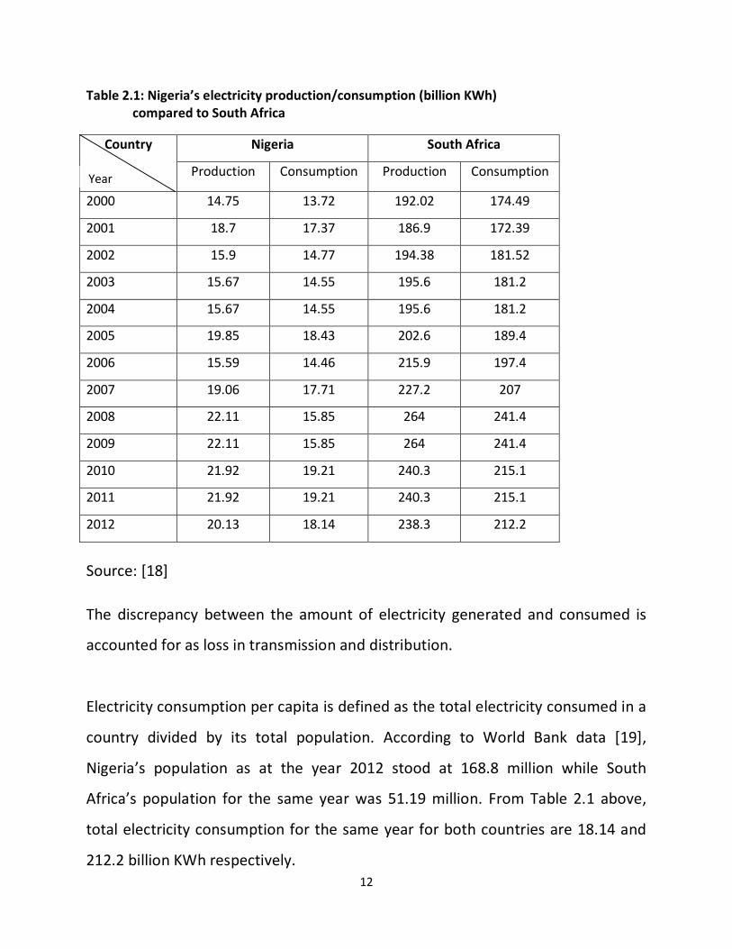
12
Table 2.1: Nigeria’s electricity production/consumption (billion KWh) compared to South Africa
Source: [18] The discrepancy between the amount of electricity generated and consumed is
accounted for as loss in transmission and distribution.
Electricity consumption per capita is defined as the total electricity consumed in a
country divided by its total population. According to World Bank data [19],
Nigeria’s population as at the year 2012 stood at 168.8 million while South
Africa’s population for the same year was 51.19 million. From Table 2.1 above,
total electricity consumption for the same year for both countries are 18.14 and
212.2 billion KWh respectively.
Country
Nigeria South Africa
Production Consumption Production Consumption
2000 14.75 13.72 192.02 174.49
2001 18.7 17.37 186.9 172.39
2002 15.9 14.77 194.38 181.52
2003 15.67 14.55 195.6 181.2
2004 15.67 14.55 195.6 181.2
2005 19.85 18.43 202.6 189.4
2006 15.59 14.46 215.9 197.4
2007 19.06 17.71 227.2 207
2008 22.11 15.85 264 241.4
2009 22.11 15.85 264 241.4
2010 21.92 19.21 240.3 215.1
2011 21.92 19.21 240.3 215.1
2012 20.13 18.14 238.3 212.2
Year

13
Therefore, electricity consumption per capita, for Nigeria and South Africa are
107.5 KWh and 4145.3KWh respectively.
From the above, a South African citizen enjoys 38.6 times more electricity than a
Nigerian. Hence, since availability of electricity in modern times translates to
economic and social development (all other factors considered), it can be argued
that South Africa has 38.6 times more potential to develop than Nigeria.
2.1 Electricity from Solar
In view of the growing demand for environmentally friendly technologies for
electricity generation, coupled with the finite nature and rising cost of fossil fuel
for conventional electricity generation, global attention has shifted to the
harnessing of renewable technologies for electricity generation [20]. Photovoltaic
solar electric generation technology is one of the best means to provide electricity
in a clean manner virtually everywhere around the world. Photovoltaic systems
are modular, producing electricity directly from sunlight and do not give rise to
emissions harmful to health or climate.
Advantages
-Environmentally friendly and pollution free (emission free).
-No use of fuels and water.
-Requires minimum maintenance and low running cost.
-Long lifetime, up to 30 years.
-Modular or “custom made” energy, can be designed for any applications from
low power to a multi-megawatt power plant.
-No restriction on harvesting as far as there is light.
14
Drawbacks
-High initial cost.
-PV cannot operate without light.
-PV generates DC current: energy storage, like batteries, and inverters are
needed.
-Large area needed for large scale applications.
-Cannot always generate stable output with ever-changing weather conditions.
In the generation of energy from solar irradiation, the PV-arrays trap the photons
of solar light and convert the light energy into electrical energy. The energy
obtained from the PV-systems can be utilized in different applications. DC power
is the direct output of PV-arrays and this DC form of power can be directly used
with DC appliances. For AC appliances, this DC power has to be changed into AC
form using power electronic inverters.
2.1.0 Components of a PV system
Photovoltaic (PV) systems consist of solar panels in addition to other hardware
usually referred to as balance of system components. The balance of system
(BOS) encompasses all components of a photovoltaic system other than the
photovoltaic panels. This includes the inverter, battery bank, charge controller,
mounting structures as well as switches, fuses, grounding equipment, combiner
boxes, wires, etc. These components are arranged and interconnected to set up a
working PV system. The system may sometimes include a solar tracking system to
improve the system's overall performance.
15
Solar panels or modules
Solar panels are made up of interconnected solar cells or photovoltaic cells that
convert the energy of light directly into electricity through a phenomenon known
as photovoltaic effect. The solar cells are the building blocks of solar panels,
otherwise known as photovoltaic modules. Each module is rated by its DC output
power under standard test conditions (STC), and typically ranges from 100 to 320
watts. The efficiency of a module determines the area of a module given the same
rated output [21]. For instance, a 16% efficient 230 watt module will have half the
area of an 8% efficient 230 watt module.
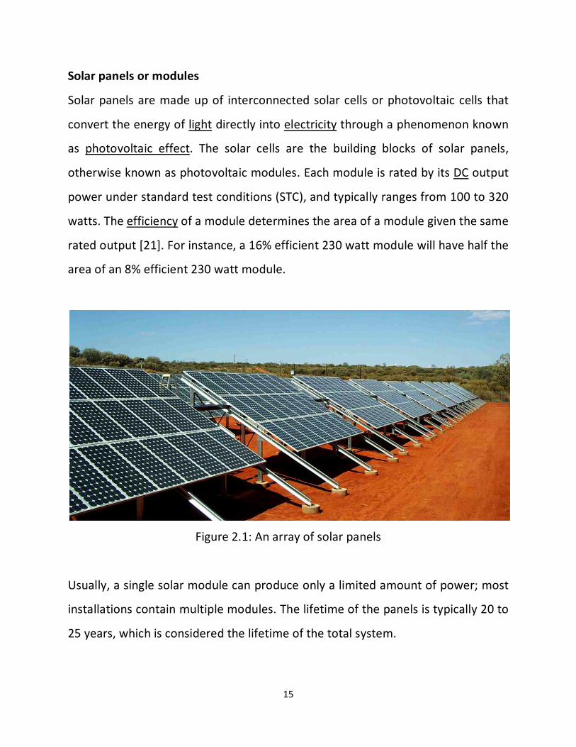
Figure 2.1: An array of solar panels
Usually, a single solar module can produce only a limited amount of power; most
installations contain multiple modules. The lifetime of the panels is typically 20 to
25 years, which is considered the lifetime of the total system.
16
Inverters
The inverter converts the Direct Current (DC) electricity produced by the solar
panels to the Alternating Current (AC) form that is required for the operation of
most electrical appliances. The converted AC can be at any required voltage and
frequency with the use of appropriate transformers, switching, and control
circuits. The inverter performs the opposite function of a rectifier.
In PV systems the inverter also provides a fail-safe link between the solar
generator and the mains electricity network. If there is a problem with the PV
system or (more usually) a fault on the electricity network, the inverter would
make the system safe. There are three types of Inverters, based on the output
waveforms. These are Square wave inverter, Modified Sine wave and Sine wave
inverter. Of these three, the Sine wave inverter has the best output waveform
obtainable from an inverter and is therefore the most suitable for all appliances.
Some of its advantages are as follows:
• Output voltage waveform is pure sine wave with very low harmonic
distortion.
• Inductive loads like microwave ovens and motors run correctly, quieter and
cooler.
• Reduces audible and electrical noise in fans, fluorescent lights, audio
amplifiers, TV, Fax, and answering machines.
• Prevents crashes in computers, unreadable print outs, and glitches and
noise in monitors.
17
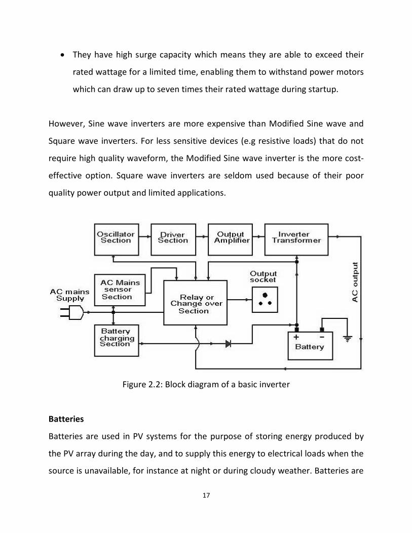
• They have high surge capacity which means they are able to exceed their
rated wattage for a limited time, enabling them to withstand power motors
which can draw up to seven times their rated wattage during startup.
However, Sine wave inverters are more expensive than Modified Sine wave and
Square wave inverters. For less sensitive devices (e.g resistive loads) that do not
require high quality waveform, the Modified Sine wave inverter is the more cost-
effective option. Square wave inverters are seldom used because of their poor
quality power output and limited applications.
Figure 2.2: Block diagram of a basic inverter
Batteries
Batteries are used in PV systems for the purpose of storing energy produced by
the PV array during the day, and to supply this energy to electrical loads when the
source is unavailable, for instance at night or during cloudy weather. Batteries are

18
rated in amp-hours. The amp-hours (AH) indicates how much energy can be
stored in by the battery. Two types of batteries can be used, deep-cycle and
starter batteries. Deep-cycle batteries are more efficient and most commonly
used, but starter batteries are widely available in Nigeria due to their use in cars.
Although not recommended for most PV applications, SLI (Starting, Lighting and
Ignition) batteries may provide up to two years of useful service in small stand-
alone PV systems where the average daily depth of discharge (DOD) is limited. SLI
batteries are designed to produce a high amount of current in a very short time.
Deep cycle batteries on the other hand are designed to produce less current than
an SLI type battery, yet they produce that current for longer periods of time.
Deep cycle batteries can be discharged up to 80 percent DOD without damage
depending on the model. In order to increase battery life, manufacturers
recommend discharging deep-cycle batteries only down to 50 percent in order to
increase battery life. A deep-cycle battery lasts between three and eight years.
Charge Controller
A charge controller is used to maintain the proper charging voltage on the
batteries in order to maximize the battery lifetime. It prevents overcharging and
may protect against overvoltage, which can reduce battery performance or
lifespan and may also pose a safety risk. Further, in order to protect battery life,
some charge controllers have additional features, such as a low voltage
disconnect (LDV), a separate circuit which powers down the load when the
batteries become overly discharged. The two major types of charge controllers in
use are: PWM (Pulse Width Modulation) and MPPT (Maximum Power Point
Tracking) charge controllers.

19
Mounting structures
The principal aim of the mounting structures is to hold the PV modules securely in
place. Arrays are most commonly mounted on roofs or on steel poles set in
concrete. In certain applications, they may be mounted at ground level or on
building walls. On roof-mounted systems, the PV array is typically mounted on
fixed racks, parallel to the roof for aesthetic reasons and stood off several inches
above the roof surface to allow airflow that will keep them as cool as possible. In
addition to cost considerations, a key requirement of mounting structures is that
they should be such that there is easy access to the modules for the maintenance
or repair.
Switches
Switches ensure that the system can be safely shut down and system components
can be removed for maintenance and repair. For grid-connected systems, a switch
ensures that the generating equipment is isolatable from the grid, which is
important for the safety of personnel. In general, a switch is needed for each
source of power or energy storage device in the system
Grounding equipment
Grounding equipment provides a well-defined, low-resistance path from your
system to the ground to protect your system from current surges from lightning
strikes or equipment malfunctions. Grounding also stabilizes voltages and
provides a common reference point. All system components and any exposed
metal, receptacles and frames should be grounded. The grounding harness is
usually located on the roof.

20
Combiner box
Wires from individual PV modules or strings are run to the combiner box, typically
located on the roof. These wires may be single conductor pigtails with connectors
that are pre-wired onto the PV modules. The output of the combiner box is one
larger two-wire conductor in conduit. A combiner box typically includes a safety
fuse or breaker for each string and may include a surge protector.
Surge protection
Surge protectors help to protect your system from power surges that may occur if
the PV system or nearby power lines are struck by lightning. A power surge is an
increase in voltage significantly above the design voltage.
2.1.1 Design Considerations
The design of a photovoltaic system must balance the rate of solar energy
deposition on a given area with the power required by the load. The measure of
total solar irradiance commonly used to assess the input for photovoltaic panels is
daily “peak sun hours”. The number of daily peak sun hours is equal to the value
in kWh of the total amount of direct and diffuse solar radiation incident on a
square meter in a day. As one moves northward through Nigeria, average
irradiance increases, despite Nigeria’s location in the northern hemisphere. This
gradient is explained by the movement of the Guinea trade winds and the
associated geographic variation in intensity and duration of the rainy and dust
storm seasons. (A study by the U.S. National Academies and the Nigerian
Academy of Science (2007) suggests that battery replacement occur during the
rainy season, in order to bolster customers’ interest in their systems when
capacity is at its lowest. In order to maintain optimal system functioning during
21
the opposite season of dusty Harmattan winds, it is important that customers
wipe the dust off their panels daily. Lagos and the rest of the coast in the south of
Nigeria receive between 3.5 and 4.0 peak sun hours at minimum. The northern
region of the country receives between 5.0 and 5.5 peak sun hours at minimum.
2.1.2 Energy from the PV module
The output power generated from the PV module, with respect to the solar
radiation, can be calculated using the following formula [22]:
Ptpv = Spv ηpv Pf ηpc Gt t=0,..,T-1
where Spv is the solar cell array area, ηpv is the module reference efficiency, Pf is
the packing factor ηpc is the power conditioning efficiency, and Gt is the hourly
irradiance.

22
Figure 2.3: Yearly minimum Peak Sun Hours
2.2 Use of Generators
Due to the lack of reliable electricity, many people and companies supplement
the electricity provided by the grid system with their own generators. According
to one approximation, well over 90% businesses have generators. The World Bank
survey of Nigerian firms in the year, 2002 shows that 95.7, 98.2 and 98.2% of
business firms located in the north, east and south of Nigeria respectively owned
private generators. In average, about 97.1% of business firms located in Nigeria
owned and operate private generator.
Generators are used not only by rural households but also by grid connected
households and industries as a more stable supplement to grid power. The rural
Source [14]
23
incidence of diesel generators is difficult to estimate, but 96 to 98% of the grid-
connected firms surveyed reported ownership of private generators [23].
For these systems, the value of the generator’s kVA rating should equal or exceed
the wattage of estimated load. The estimated lifetime of a generator is between
10 and 13 years. When calculating the present value of the lifetime costs of fuel,
one must consider not only the rising cost of petrodiesel due to Nigeria’s limited
refining capacity, but also the disparity in Nigeria’s official, subsidized price of
diesel and the significantly higher price that can be obtained in practice, which
ranges from 1.5 to 4 times the official price.
The actual market price of diesel is likely highest for the most remote regions.
(See Oparaku (2003) for a sensitivity analysis of the life-cycle cost of the entire
system with variation in fuel price).
2.3 Transfer Switches
Transfer (or changeover) switches allow switching from a primary power source
to a secondary or tertiary power source and are employed in some electrical
power distribution systems; most often transfer switches can be seen where
emergency power generators are used to back up from the utility source. The
transfer switching allows safe switching from utility power to emergency
generator power while maintaining isolation of each source from the other. The
switch may be a manual switch, an automatic switch or a combination of manual
and automatic. In a home, for example, during power outages, the power transfer
switch allows isolation of the owner’s critical circuits (e.g. cooling, refrigerator,
lighting) from the utility service, hence allowing for operation of the generator
without back feeding to the utility which can damage utility equipment [24].
24
Standby generation systems in low- and medium-voltage applications connect to
the utility power system in a number of different ways. Typically, an automatic
transfer switch is a part of most power system connections. Automatic transfer
switches (ATS) continually monitor the incoming utility power automatically. Any
anomalies such as voltage drops, brownouts spikes, or surges will cause the
internal circuitry to signal a generator to start. This will then transfer to the
generator when additional switch circuitry determines that the generator has the
proper voltage and frequency. When utility power returns and no anomalies
occur for a certain time, the transfer switch will then transfer load back to the
utility line and initiate the turn off of the generator.
2.3.0 Types of Transfer Switches
1. Open Transition Transfer Switch (OTTS)
An Open Transition Switch is also called a ‘break before make’ transfer switch. A
‘break before make’ transfer switch breaks contacts with one source of power
before it makes contacts with another, and therefore it prevents back feeding
from an emergency generator back into the utility line, for example. One example
is an open transition automatic transfer switch (ATS). During the slip second of
the power transfer the flow of electricity is interrupted.
2. Closed Transition Transfer Switch (CTTS).
A Closed transition transfer switch is also called a ‘make before break’ transfer
switch. In a typical emergency system, there is an inherent momentary
interruption of power to the load when it is transferred from one available source
to another. In most cases this outage is inconsequential, particularly if it is less
than 1/6 of a second. There are some loads however, that are affected by even
25
the slightest loss of power. There are also operational conditions where it may be
desirable to transfer loads with zero interruption of power when condition
permit. For these applications, closed transition transfer switches can be
provided. When transferring loads in this manner, during a test or when re-
transferring to normal after primary power has stabilized, the switch will operate
in a make-before break mode provided both sources are acceptable and
synchronized. Typical parameters determining synchronization are: voltage
difference less than 5%, frequency difference less than 0.2Hz and relative phase
angle between the sources of 5 electrical degrees. Since the maximum frequency
difference is 0.2Hz, the engine will generally be required to be controlled by an
isochronous governor.
It is generally required that the closed transition, or overlap time, be less than 100
milliseconds. If either source is not present or not acceptable (such as when
normal power fails) the switch must operate in a break before make less mode
(standard open transition operation) to ensure no back feeding occurs. Closed
transition transfer makes code-mandated monthly testing less objectionable
because it eliminates the interruptions to critical loads, which occur during
traditional open transition transfer.
2.3.1 Applications of Closed Transition Transfer Switch (CTTS)
Typical load switching application for which closed transition transfer is desirable
includes data processing and electronic load. Certain motor and transformer
loads, curtailment systems, or anywhere load interruptions of even the shortest
duration are objectionable. It should be understood that a CTTS in a system is not
a substitute for a UPS (uninterrupted power supply). In addition to providing line
conditioning, a UPS has a built-in stored energy that provides power for a
26
prescribed period of time in the event of a power failure. A CTTS by itself simply
assures that there will be no momentary loss of power when the load is
transferred from one live power source to another.
2.4 Uninterruptible Power Supplies (UPS)
In today’s mission-critical applications, where the end-use equipment cannot
tolerate even a momentary power outage and, even relatively minor disturbances
in the power system can cause computer systems to re-boot, uninterruptible
power supplies are used to provide continuous, conditioned power to sensitive
loads, thereby preventing operational down-time.
UPS’s use stored energy, usually chemical energy in the form of batteries or
mechanical energy in the form of a rotating flywheel, and use it to “bridge the
gap” from the time the normal source of power (i.e., the utility) fails and the time
the alternate source of power (standby generators, solar) can be brought on-line.
In addition, many UPS systems provide power conditioning, further isolating the
sensitive loads from disturbances on the system. However, the UPS stored energy
source cannot operate indefinitely, and typically requires re-charging from the
system normal or alternate power source.
2.5 Microcontroller and Embedded systems
A microcontroller is a small computer on a single integrated circuit containing a
processor core, memory, and programmable input/output peripherals. It can be
considered as a microcomputer built on a single integrated circuit or chip [25].
Microcontrollers are designed for embedded applications, in contrast to the
microprocessors used in personal computers or other general purpose

27
applications. Modern high-performance embedded processors are capable of a
great deal of computation in addition to I/O tasks [26]. Dramatic advances in
computer and communication technologies have made it economically feasible to
extend the use of embedded systems to more and more critical applications [27].
2.5.0 The 89C52 Microcontroller
The AT89C52 used in this design is a low-power, high-performance CMOS 8-bit
microcomputer with 8K bytes of Flash programmable and erasable read only
memory (PEROM) manufactured by Atmel. It is compatible with the industry-
standard 80C51 and 80C52 instruction set and pinout. The on-chip Flash allows
the program memory to be reprogrammed in-system or by a conventional
nonvolatile memory programmer. By combining a versatile 8-bit CPU with Flash
on a monolithic chip, the Atmel AT89C52 is a powerful microcomputer which
provides a highly-flexible and cost-effective solution to many embedded control
applications.
28
Figure 2.4: Pin designation of AT89C52 microcontroller
The AT89C52 provides the following standard features: 8K bytes of Flash, 256
bytes of RAM, 32 I/O lines, three 16-bit timer/counters, a six-vector two-level
interrupt architecture, a full-duplex serial port, on-chip oscillator, and clock
circuitry. In addition, the AT89C52 is designed with static logic for operation down
to zero frequency and supports two software selectable power saving modes. The
Idle Mode stops the CPU while allowing the RAM, timer/counters, serial port, and
interrupt system to continue functioning. The Power-down mode saves the RAM
contents but freezes the oscillator, disabling all other chip functions until the next
hardware reset.

29
Pin Description
VCC
Supply voltage.
GND
Ground.
Port 0
Port 0 is an 8-bit open drain bi-directional I/O port. As an output port, each pin
can sink eight TTL inputs. When 1s are written to port 0 pins, the pins can be used
as high impedance inputs. Port 0 can also be configured to be the multiplexed low
order address/data bus during accesses to external program and data memory. In
this mode, P0 has internal pull-ups. Port 0 also receives the code bytes during
Flash programming and outputs the code bytes during program verification.
External pull-ups are required during program verification.
Port 1
Port 1 is an 8-bit bi-directional I/O port with internal pull-ups. The Port 1 output
buffers can sink/source four TTL inputs. When 1s are written to Port 1 pins, they
are pulled high by the internal pull-ups and can be used as inputs. As inputs, Port
1 pins that are externally being pulled low will source current (IIL) because of the
internal pull-ups. In addition, P1.0 and P1.1 can be configured to be the
timer/counter 2 external count input (P1.0/T2) and the timer/counter 2 trigger
input (P1.1/T2EX), respectively, as shown in the following table. Port 1 also
receives the low-order address bytes during Flash programming and verification.

30
Port 2
Port 2 is an 8-bit bi-directional I/O port with internal pull-ups. The Port 2 output
buffers can sink/source four TTL inputs. When 1s are written to Port 2 pins, they
are pulled high by the internal pull-ups and can be used as inputs. As inputs, Port
2 pins that are externally being pulled low will source current (IIL) because of the
internal pull-ups. Port 2 emits the high-order address byte during fetches from
external program memory and during accesses to external data memory that use
16-bit addresses (MOVX @ DPTR). In this application, Port 2 uses strong internal
pull-ups when emitting 1s. During accesses to external data memory that use 8-
bit addresses (MOVX @ RI), Port 2 emits the contents of the P2 Special Function
Register. Port 2 also receives the high-order address bits and some control signals
during Flash programming and verification.
Port 3
Port 3 is an 8-bit bi-directional I/O port with internal pull-ups. The Port 3 output
buffers can sink/source four TTL inputs. When 1s are written to Port 3 pins, they
are pulled high by the internal pull-ups and can be used as inputs. As inputs, Port
3 pins that are externally being pulled low will source current (IIL) because of the
pull-ups. Port 3 also serves the functions of various special features of the
AT89C51, as shown in the following table. Port 3 also receives some control
signals for Flash programming and verification. Reset input. A high on this pin for
two machine cycles while the oscillator is running resets the device.
ALE/PROG
Address Latch Enable is an output pulse for latching the low byte of the address
during accesses to external memory. This pin is also the program pulse input
(PROG) during Flash programming. In normal operation, ALE is emitted at a

31
constant rate of 1/6 the oscillator frequency and may be used for external timing
or clocking purposes. Note, however, that one ALE pulse is skipped during each
access to external data memory. If desired, ALE operation can be disabled by
setting bit 0 of SFR location 8EH. With the bit set, ALE is active only during a
MOVX or MOVC instruction. Otherwise, the pin is weakly pulled high. Setting the
ALE-disable bit has no effect if the microcontroller is in external execution mode.
PSEN
Program Store Enable is the read strobe to external program memory. When the
AT89C52 is executing code from external program memory, PSEN is activated
twice each machine cycle, except that two PSEN activations are skipped during
each access to external data memory.
EA/VPP
External Access Enable. EA must be strapped to GND in order to enable the device
to fetch code from external program memory locations starting at 0000H up to
FFFFH. Note, however, that if lock bit 1 is programmed, EA will be internally
latched on reset. EA should be strapped to VCC for internal program executions.
This pin also receives the 12-volt programming enable voltage (VPP) during Flash
programming when 12-volt programming is selected.
XTAL1
Input to the inverting oscillator amplifier and input to the internal clock operating
circuit.
XTAL2
Output from the inverting oscillator amplifier.
32
Special Function Registers
A map of the on-chip memory area called the Special Function Register (SFR)
space is shown in Table 2.2. Note that not all of the addresses are occupied, and
unoccupied addresses may not be implemented on the chip. Read accesses to
these addresses will in general return random data, and write accesses will have
an indeterminate effect. User software should not write 1s to these unlisted
locations, since they may be used in future products to invoke new features. In
that case, the reset or inactive values of the new bits will always be 0.
Table 2.2: AT89C52 SFR Map and Reset Values
33
Timer 2 Registers Control and status bits are contained in registers T2CON (shown
in Table 2.3) and T2MOD (shown in Table 2.5) for Timer 2. The register pair
(RCAP2H, RCAP2L) are the Capture/Reload registers for Timer 2 in 16-bit capture
mode or 16-bit auto-reload mode.
Table 2.3: T2CON – Timer/Counter 2 Control Register
Table 2.4: Timer 2 Operating Modes
Interrupt Registers The individual interrupt enable bits are in the IE register. Two
priorities can be set for each of the six interrupt sources in the IP register.
34
Data Memory
The AT89C52 implements 256 bytes of on-chip RAM. The upper 128 bytes occupy
a parallel address space to the Special Function Registers. That means the upper
128 bytes have the same addresses as the SFR space but are physically separate
from SFR space. When an instruction accesses an internal location above address
7FH, the address mode used in the instruction specifies whether the CPU accesses
the upper 128 bytes of RAM or the SFR space. Instructions that use direct
addressing access SFR space. For example, the following direct addressing
instruction accesses the SFR at location 0A0H (which is P2).
MOV 0A0H, #data
Instructions that use indirect addressing access the upper 128 bytes of RAM. For
example, the following indirect addressing instruction, where R0 contains 0A0H,
accesses the data byte at address 0A0H, rather than P2 (whose address is 0A0H).
MOV @R0, #data
Note that stack operations are examples of indirect addressing, so the upper 128
bytes of data RAM are available as stack space.
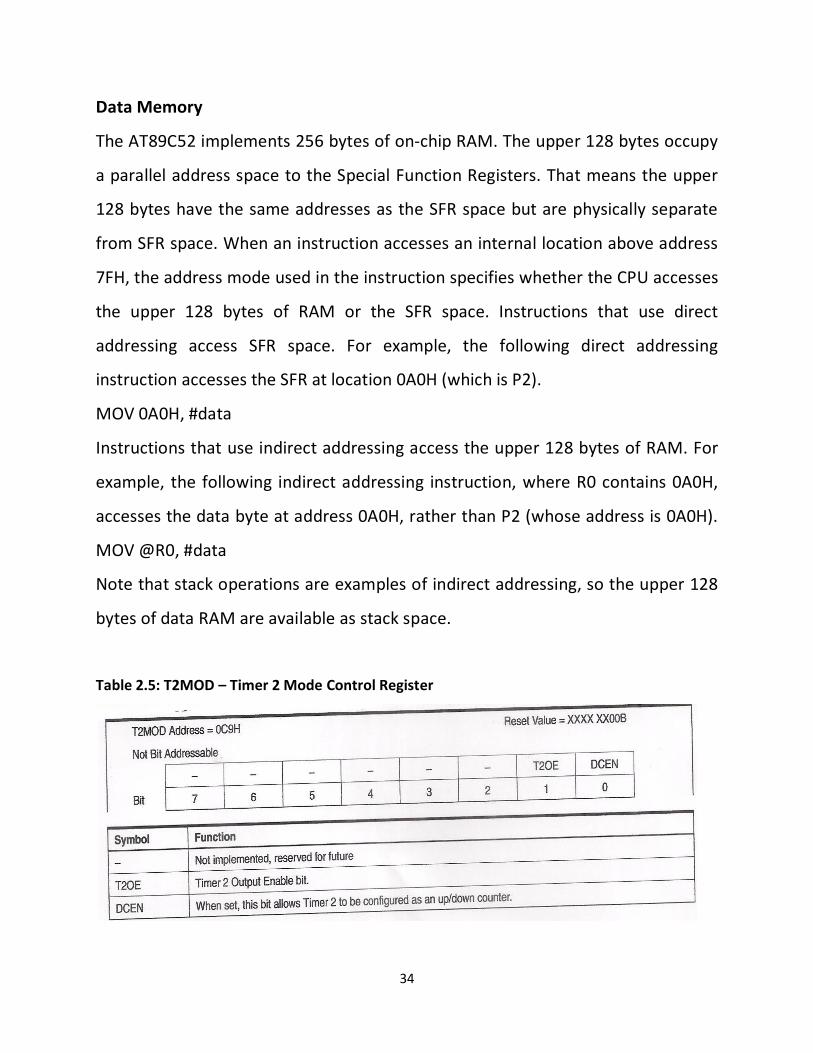
Table 2.5: T2MOD – Timer 2 Mode Control Register
35
Timer 0 and 1
Timer 0 and Timer 1 in the AT89C52 operate the same way as Timer 0 and Timer 1
in the AT89C51.
Timer 2
Timer 2 is a 16-bit Timer/Counter that can operate as either a timer or an event
counter. The type of operation is selected by bit C/T2 in the SFR T2CON (shown in
Table 2.3). Timer 2 has three operating modes: capture, auto-reload (up or down
counting), and baud rate generator. The modes are selected by bits in T2CON, as
shown in Table 2.4. Timer 2 consists of two 8-bit registers, TH2 and TL2. In the
Timer function, the TL2 register is incremented every machine cycle. Since a
machine cycle consists of 12 oscillator periods, the count rate is 1/12 of the
oscillator frequency. In the Counter function, the register is incremented in
response to a 1-to-0 transition at its corresponding external input pin, T2. In this
function, the external input is sampled during S5P2 of every machine cycle. When
the samples show a high in one cycle and a low in the next cycle, the count is
incremented. The new count value appears in the register during S3P1 of the
cycle following the one in which the transition was detected. Since two machine
cycles (24 oscillator periods) are required to recognize a 1-to-0 transition, the
maximum count rate is 1/24 of the oscillator frequency. To ensure that a given
level is sampled at least once before it changes, the level should be held for at
least one full machine cycle.
Capture Mode
In the capture mode, two options are selected by bit EXEN2 in T2CON. If EXEN2 =
0, Timer 2 is a 16-bit timer or counter which upon overflow sets bit TF2 in T2CON.
36
This bit can then be used to generate an interrupt. If EXEN2 = 1, Timer 2 performs
the same operation, but a 1-to-0 transition at external input T2EX also causes the
current value in TH2 and TL2 to be captured into RCAP2H and RCAP2L,
respectively. In addition, the transition at T2EX causes bit EXF2 in T2CON to be
set. The EXF2 bit, like TF2, can generate an interrupt.
Auto-reload (Up or Down Counter)
Timer 2 can be programmed to count up or down when configured in its 16-bit
auto-reload mode. This feature is invoked by the DCEN (Down Counter Enable) bit
located in the SFR T2MOD (see Table 4). Upon reset, the DCEN bit is set to 0 so
that timer 2 will default to count up. When DCEN is set, Timer 2 can count up or
down, depending on the value of the T2EX pin.
Baud Rate Generator
Timer 2 is selected as the baud rate generator by setting TCLK and/or RCLK in
T2CON (Table 2.3). Note that the baud rates for transmit and receive can be
different if Timer 2 is used for the receiver or transmitter and Timer 1 is used for
the other function.
The baud rate generator mode is similar to the auto-reload mode, in that a
rollover in TH2 causes the Timer 2 registers to be reloaded with the 16-bit value in
registers RCAP2H and RCAP2L, which are preset by software. The baud rates in
Modes 1 and 3 are determined by Timer 2’s overflow rate according to the
following equation.
Modes 1 and 3 Baud Rates =Timer 2 Overlow Rate
16
37
The Timer can be configured for either timer or counter operation. In most
applications, it is configured for timer operation (CP/T2 = 0). The timer operation
is different for Timer 2 when it is used as a baud rate generator. Normally, as a
timer, it increments every machine cycle (at 1/12 the oscillator frequency). As a
baud rate generator, however, it increments every state time (at 1/2 the oscillator
frequency). The baud rate formula is given below.
Modes 1 and 3 Baud Rate
=TimeOscillator Frequency
32 x [65536 − (RECAP2H, RECAP2L)]
where (RCAP2H, RCAP2L) is the content of RCAP2H andRCAP2L taken as a 16-bit
unsigned integer. Timer 2 as a baud rate generator is shown in Figure 4. This
figure is valid only if RCLK or TCLK = 1 in T2CON. Note that a rollover in TH2 does
not set TF2 and will not generate an interrupt. Note too, that if EXEN2 is set, a 1-
to-0 transition in T2EX will set EXF2 but will not cause a reload from (RCAP2H,
RCAP2L) to (TH2, TL2). Thus when Timer 2 is in use as a baud rate generator, T2EX
can be used as an extra external interrupt. Note that when Timer 2 is running
(TR2 = 1) as a timer in the baud rate generator mode, TH2 or TL2 should not be
read from or written to. Under these conditions, the Timer is incremented every
state time, and the results of a read or write may not be accurate. The RCAP2
registers may be read but should not be written to, because a write might overlap
a reload and cause write and/or reload errors. The timer should be turned off
(clear TR2) before accessing the Timer 2 or RCAP2 registers.
38
2.6 Comparator
A comparator is similar to an op amp which is arguably the most useful single
device in analog electronic circuitry [28]. It has two inputs, inverting and non-
inverting and an output. But it is specifically designed to compare the voltages
between its two inputs. Therefore it operates in a non-linear fashion.
Comparators generally have more flexible output circuits than op-amps. Whereas
an ordinary op-amp uses a push-pull output stage to swing between the supply
voltages, a comparator chip usually has an open-collector output with grounded
emitter [29]. The comparator operates open-loop, providing a two-state logic
output voltage. These two states represent the sign of the net difference between
the two inputs (including the effects of the comparator input offset voltage).
Therefore, the comparator's output will be a logic "1" if the input signal on the
non-inverting input exceeds the signal on the inverting input (plus the offset
voltage, Vos) and a logic "0" for the opposite case. A comparator is normally used
in applications where some varying signal level is compared to a fixed level
(usually a voltage reference). Since it is, in effect, a 1-bit analog-to-digital
converter (ADC), the comparator is a basic element in all ADCs [30].
Because comparators have only two output states, their outputs are near zero or
near the supply voltage. Bipolar rail-to-rail comparators have a common-emitter
output that produces a small voltage drop between the output and each rail. That
drop is equal to the collector-to-emitter voltage of a saturated transistor. When
output currents are light, output voltages of CMOS rail-to-rail comparators, which
rely on a saturated MOSFET, range closer to the rails than their bipolar
counterparts.
39
On the basis of outputs, comparators can also be classified as open drain or push–
pull. Comparators with an open-drain output stage use an external pull up resistor
to a positive supply that defines the logic high level. Open drain comparators are
more suitable for mixed-voltage system design. Since the output is high
impedance for logic level high, open drain comparators can also be used to
connect multiple comparators on to a single bus. Push pull output does not need
a pull up resistor and can also source current unlike an open drain output.
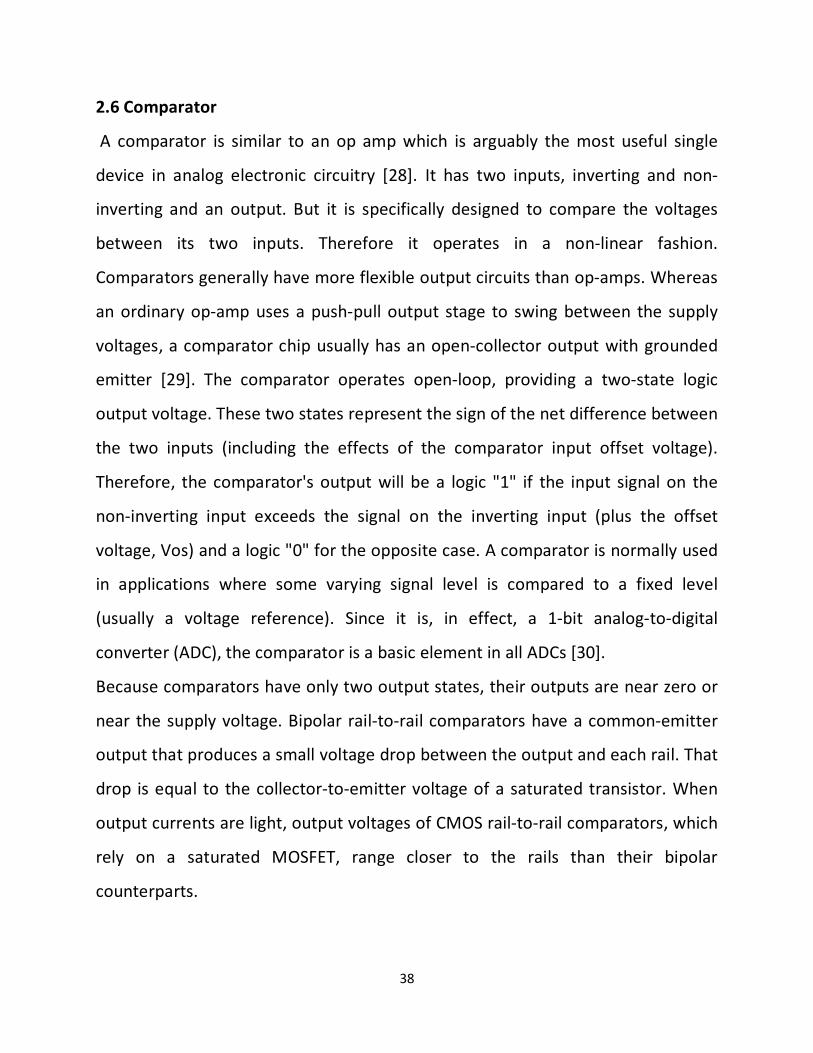
The pin diagram of LM339 is shown in figure 2.5 below. LM339 is a comparator IC
with four inbuilt comparators.
Figure 2.5: LM339 Pin Configuration
2.6.0 Comparator parameters
The major comparator parameters include the following: Propagation delay,
Current consumption, Output stage type (open collector/drain or push-pull), Input
offset voltage, hysteresis, Output current capability, Rise and fall time, Input
common mode voltage range.
40
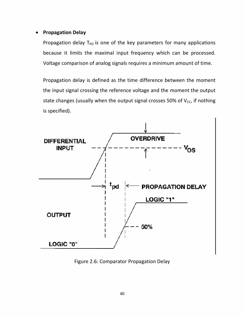
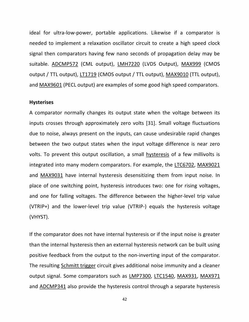
• Propagation Delay
Propagation delay TPD is one of the key parameters for many applications
because it limits the maximal input frequency which can be processed.
Voltage comparison of analog signals requires a minimum amount of time.
Propagation delay is defined as the time difference between the moment
the input signal crossing the reference voltage and the moment the output
state changes (usually when the output signal crosses 50% of VCC, if nothing
is specified).
Figure 2.6: Comparator Propagation Delay
41
The propagation delay in practical comparators decreases somewhat as the
input overdrive is increased. This variation in propagation delay as a function
of overdrive is called dispersion.
• Voltage Gain
Voltage gain AVD indicates the overall device gain. Higher gain means better
small input signal resolving capability which can be an advantage in certain
applications. Common comparators have an AVD in the range of 200 V/mV (106
dB). 1 mV input signal amplified by 106 dB leads to theoretical amplitude of
200 V. In reality, the output signal swing is limited by VCC. Note that the AVD
doesn’t affect external hysteresis as the output is always in high or low state
and never between (unlike an operational amplifier, a comparator is not used
in its linear region).
• Input Offset Voltage
The input offset voltage (VIO) can be defined as the differential input voltage to
apply in order to be at the toggling level. Input offset voltage limits the resolution
of comparators. Therefore, for very small signals (in the same order as the VIO),
the comparator toggles at an undesired value or does not toggle at all.
Speed and Power
While in general comparators are "fast," their circuits are not immune to the
classic speed-power tradeoff. High speed comparators use transistors with larger
aspect ratios and hence also consume more power. Depending on the application,
select either a comparator with high speed or one that saves power. For example,
nano-powered comparators in space-saving chip-scale packages (UCSP), DFN or
SC70 packages such as MAX9027, LTC1540, LPV7215, MAX9060 and MCP6541 are
42
ideal for ultra-low-power, portable applications. Likewise if a comparator is
needed to implement a relaxation oscillator circuit to create a high speed clock
signal then comparators having few nano seconds of propagation delay may be
suitable. ADCMP572 (CML output), LMH7220 (LVDS Output), MAX999 (CMOS
output / TTL output), LT1719 (CMOS output / TTL output), MAX9010 (TTL output),
and MAX9601 (PECL output) are examples of some good high speed comparators.
Hysterises
A comparator normally changes its output state when the voltage between its
inputs crosses through approximately zero volts [31]. Small voltage fluctuations
due to noise, always present on the inputs, can cause undesirable rapid changes
between the two output states when the input voltage difference is near zero
volts. To prevent this output oscillation, a small hysteresis of a few millivolts is
integrated into many modern comparators. For example, the LTC6702, MAX9021
and MAX9031 have internal hysteresis desensitizing them from input noise. In
place of one switching point, hysteresis introduces two: one for rising voltages,
and one for falling voltages. The difference between the higher-level trip value
(VTRIP+) and the lower-level trip value (VTRIP-) equals the hysteresis voltage
(VHYST).
If the comparator does not have internal hysteresis or if the input noise is greater
than the internal hysteresis then an external hysteresis network can be built using
positive feedback from the output to the non-inverting input of the comparator.
The resulting Schmitt trigger circuit gives additional noise immunity and a cleaner
output signal. Some comparators such as LMP7300, LTC1540, MAX931, MAX971
and ADCMP341 also provide the hysteresis control through a separate hysteresis
43
pin. These comparators make it possible to add a programmable hysteresis
without feedback or complicated equations. Using a dedicated hysteresis pin is
also convenient if the source impedance is high since the inputs are isolated from
the hysteresis network. When hysteresis is added then a comparator cannot
resolve signals within the hysteresis band.
2.6.1 Comparator applications
Null detectors
A null detector is one that functions to identify when a given value is zero.
Comparators can be a type of amplifier distinctively for null comparison
measurements. It is the equivalent to a very high gain amplifier with well-
balanced inputs and controlled output limits. The circuit compares the two input
voltages, determining the larger. The inputs are an unknown voltage and a
reference voltage, usually referred to as vu and vr. A reference voltage is generally
on the non-inverting input (+), while vu is usually on the inverting input (−). (A
circuit diagram would display the inputs according to their sign with respect to
the output when a particular input is greater than the other.) The output is either
positive or negative, for example ±12 V. In this case, the idea is to detect when
there is no difference between in the input voltages. This gives the identity of the
unknown voltage since the reference voltage is known.
When using a comparator as a null detector, there are limits as to the accuracy of
the zero value measurable. Zero output is given when the magnitude of the
difference in the voltages multiplied by the gain of the amplifier is less than the
voltage limits. For example, if the gain of the amplifier is 106, and the voltage
44
limits are ±6 V, then no output will be given if the difference in the voltages is less
than 6 μV. One could refer to this as a sort of uncertainty in the measurement.
Zero-crossing detectors
For this type of detector, a comparator detects each time an ac pulse changes
polarity. The output of the comparator changes state each time the pulse changes
its polarity, that is the output is HI (high) for a positive pulse and LO (low) for a
negative pulse squares the input signal.
Relaxation oscillator
A comparator can be used to build a relaxation oscillator. It uses both positive and
negative feedback. The positive feedback is a Schmitt trigger configuration. Alone,
the trigger is a bistable multivibrator. However, the slow negative feedback added
to the trigger by the RC circuit causes the circuit to oscillate automatically. That is,
the addition of the RC circuit turns the hysteretic bistable multivibrator into an
astable multivibrator.
Level shifter
This circuit requires only a single comparator with an open-drain output as in the
LM393, TLV3011 or MAX9028. The circuit provides great flexibility in choosing the
voltages to be translated by using a suitable pull up voltage. It also allows the
translation of bipolar ±5 V logic to unipolar 3 V logic by using a comparator like
the MAX972.
45
Analog-to-digital converters
When a comparator performs the function of telling if an input voltage is above or
below a given threshold, it is essentially performing a 1-bit quantization. This
function is used in nearly all analog to digital converters (such as flash, pipeline,
successive approximation, delta-sigma modulation, folding, interpolating, dual-
slope and others) in combination with other devices to achieve a multi-bit
quantization.
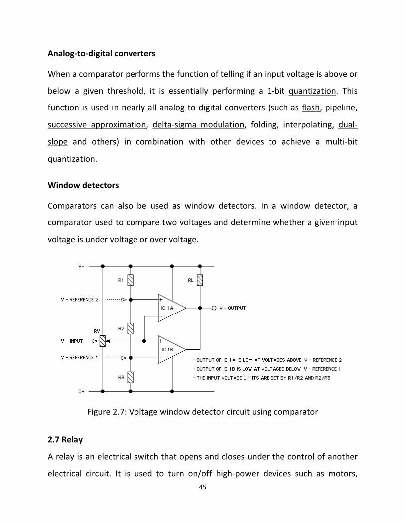
Window detectors
Comparators can also be used as window detectors. In a window detector, a
comparator used to compare two voltages and determine whether a given input
voltage is under voltage or over voltage.
Figure 2.7: Voltage window detector circuit using comparator
2.7 Relay
A relay is an electrical switch that opens and closes under the control of another
electrical circuit. It is used to turn on/off high-power devices such as motors,
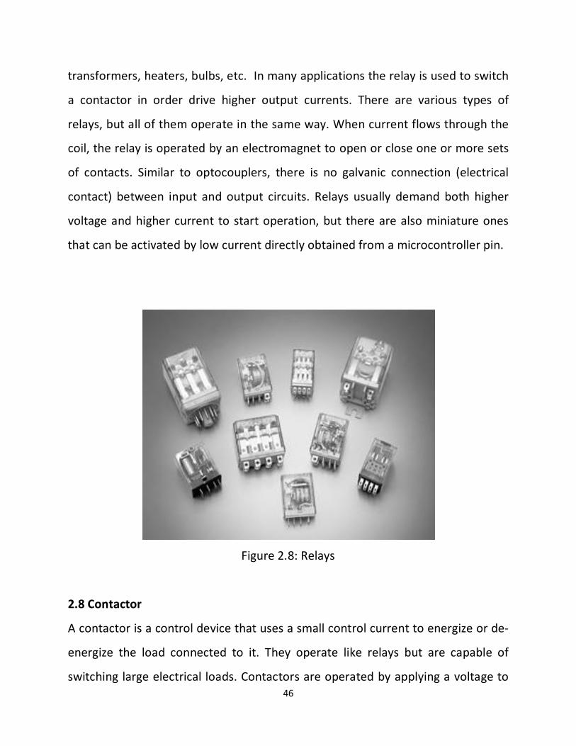
46
transformers, heaters, bulbs, etc. In many applications the relay is used to switch
a contactor in order drive higher output currents. There are various types of
relays, but all of them operate in the same way. When current flows through the
coil, the relay is operated by an electromagnet to open or close one or more sets
of contacts. Similar to optocouplers, there is no galvanic connection (electrical
contact) between input and output circuits. Relays usually demand both higher
voltage and higher current to start operation, but there are also miniature ones
that can be activated by low current directly obtained from a microcontroller pin.
Figure 2.8: Relays
2.8 Contactor
A contactor is a control device that uses a small control current to energize or de-
energize the load connected to it. They operate like relays but are capable of
switching large electrical loads. Contactors are operated by applying a voltage to
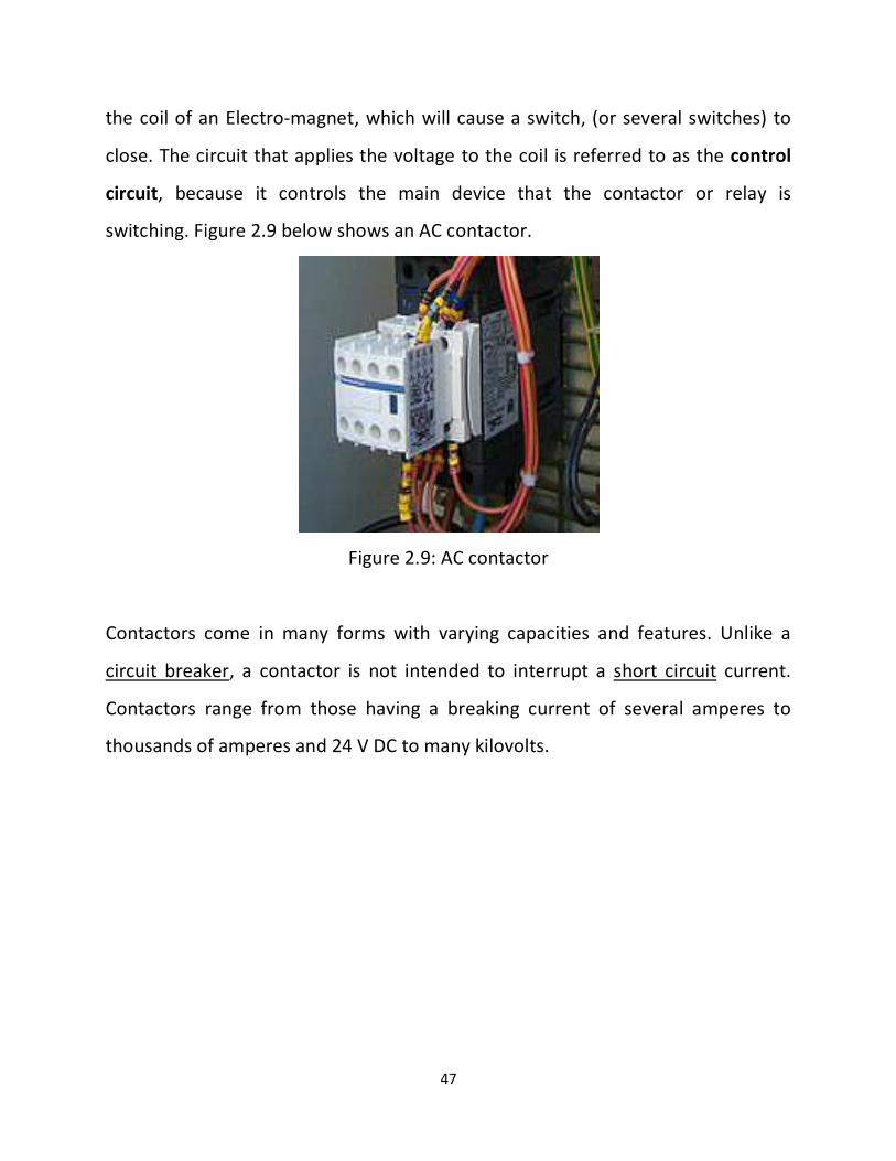
47
the coil of an Electro-magnet, which will cause a switch, (or several switches) to
close. The circuit that applies the voltage to the coil is referred to as the control
circuit, because it controls the main device that the contactor or relay is
switching. Figure 2.9 below shows an AC contactor.
Figure 2.9: AC contactor
Contactors come in many forms with varying capacities and features. Unlike a
circuit breaker, a contactor is not intended to interrupt a short circuit current.
Contactors range from those having a breaking current of several amperes to
thousands of amperes and 24 V DC to many kilovolts.
48
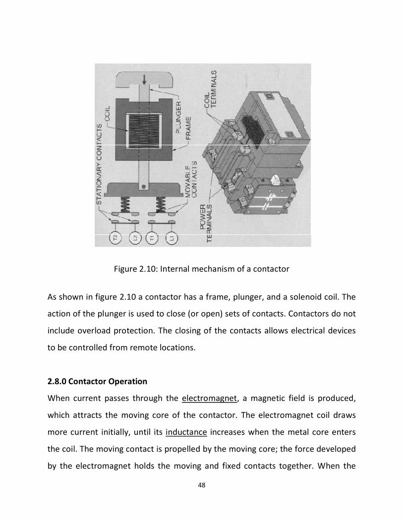
Figure 2.10: Internal mechanism of a contactor
As shown in figure 2.10 a contactor has a frame, plunger, and a solenoid coil. The
action of the plunger is used to close (or open) sets of contacts. Contactors do not
include overload protection. The closing of the contacts allows electrical devices
to be controlled from remote locations.
2.8.0 Contactor Operation
When current passes through the electromagnet, a magnetic field is produced,
which attracts the moving core of the contactor. The electromagnet coil draws
more current initially, until its inductance increases when the metal core enters
the coil. The moving contact is propelled by the moving core; the force developed
by the electromagnet holds the moving and fixed contacts together. When the
49
contactor coil is de-energized, gravity or a spring returns the electromagnet core
to its initial position and opens the contacts.
Because arcing and consequent damage occurs just as the contacts are opening or
closing, contactors are designed to open and close very rapidly; there is often an
internal tipping point mechanism to ensure rapid action.
2.9 Step down transformer
A transformer is a static (or stationary) piece of apparatus by means of which
electric power in circuit is transformed into electric power of the same frequency
in another circuit [32]. They consist of two or more coils of wire coupled together
by means of electromagnetic induction. It is based on two principles; firstly,
electric current can produce a magnetic field and secondly electromagnetic
induction. Current variation in the primary winding changes the magnetic flux that
is developed, thereby inducing a voltage in the secondary winding. The primary
winding is connected to the power source and the other windings are known as
secondary windings, which connected to the load. The behavior of a transformer
is strongly affected by the nature of the core upon which the two coils are wound.
If the core is made from some non- magnetic material (air), the component is
referred to as an air- cored transformer. If the core is made from magnetic
materials, the two windings have very much increased magnetic coupling and the
component is known as iron-cored transformer. The equation of an ideal
transformer is given as:
=NsNp
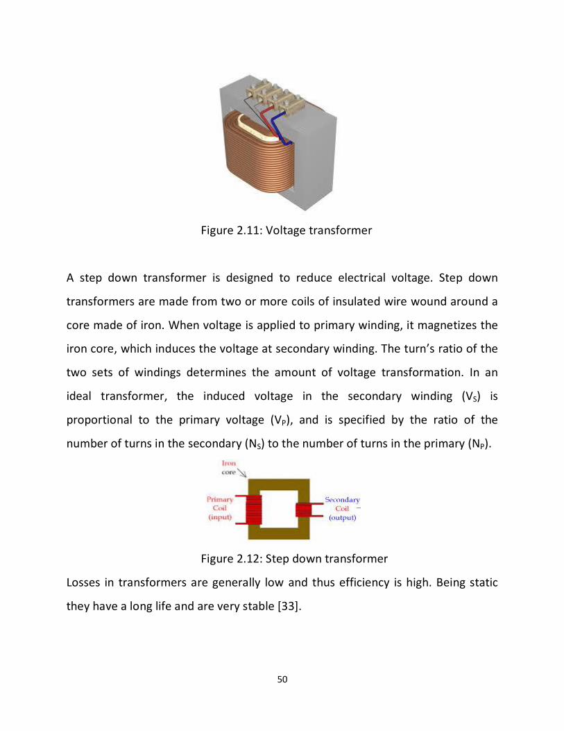
50
Figure 2.11: Voltage transformer
A step down transformer is designed to reduce electrical voltage. Step down
transformers are made from two or more coils of insulated wire wound around a
core made of iron. When voltage is applied to primary winding, it magnetizes the
iron core, which induces the voltage at secondary winding. The turn’s ratio of the
two sets of windings determines the amount of voltage transformation. In an
ideal transformer, the induced voltage in the secondary winding (VS) is
proportional to the primary voltage (VP), and is specified by the ratio of the
number of turns in the secondary (NS) to the number of turns in the primary (NP).
Figure 2.12: Step down transformer
Losses in transformers are generally low and thus efficiency is high. Being static
they have a long life and are very stable [33].
51
CHAPTER THREE
METHODOLOGY
3.0 Introduction
The system design is such that three interconnected power sources: PHCN, solar
and generator are constantly monitored with the aim to engage and utilize the
preferred power source following preset conditions in the microcontroller. In
addition to the microcontroller, the project employs the use of contactors, relays,
comparators and overloads devices which are all readily available in the market.
The design employs a priority based Automated Switching system using the
microcontroller to give preference in the desired order. Shown below is the
Priority Table for automatic input selection.
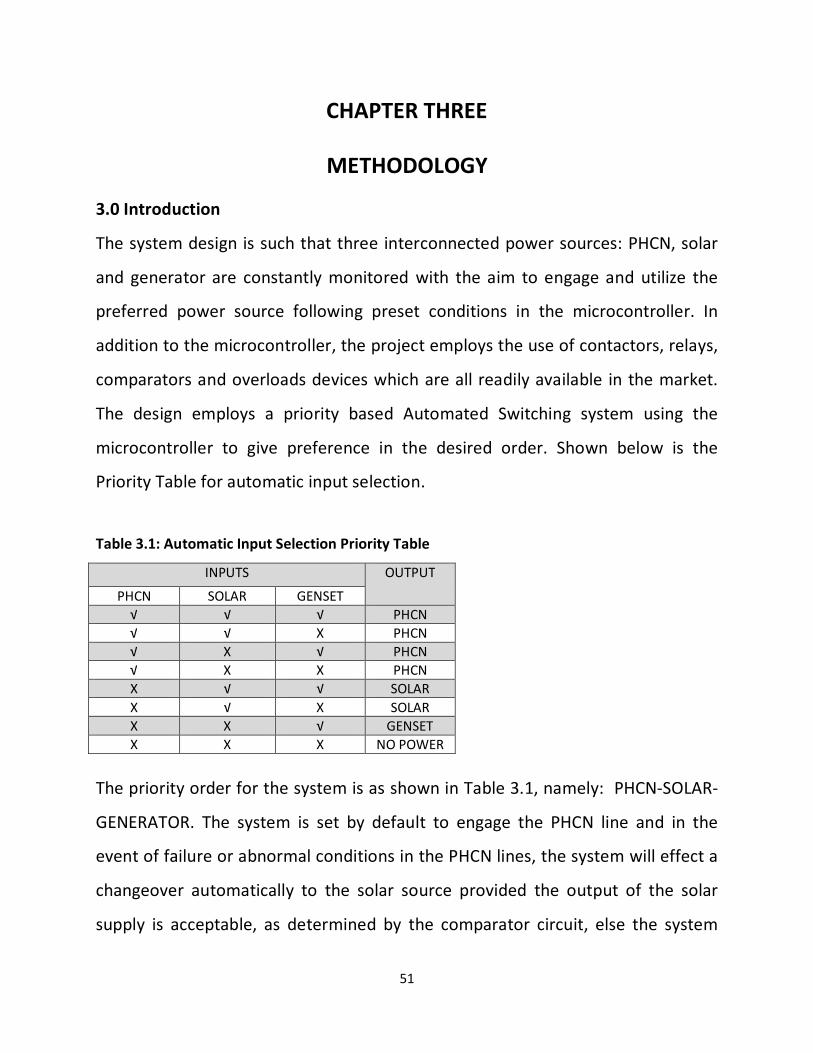
Table 3.1: Automatic Input Selection Priority Table
INPUTS OUTPUT
PHCN SOLAR GENSET √ √ √ PHCN √ √ Х PHCN √ Х √ PHCN √ Х Х PHCN Х √ √ SOLAR Х √ Х SOLAR Х Х √ GENSET Х Х Х NO POWER
The priority order for the system is as shown in Table 3.1, namely: PHCN-SOLAR-
GENERATOR. The system is set by default to engage the PHCN line and in the
event of failure or abnormal conditions in the PHCN lines, the system will effect a
changeover automatically to the solar source provided the output of the solar
supply is acceptable, as determined by the comparator circuit, else the system

52
will initiate the starting of the generator and transfer of load to same. The block
diagram of the system is as shown in the figures below.
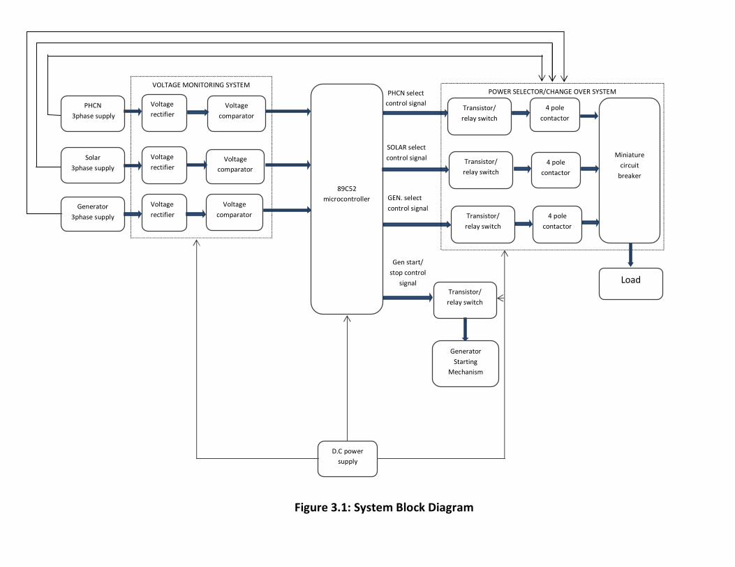
53
D.C power supply
Generator Starting
Mechanism
89C52 microcontroller
Transistor/ relay switch
PHCN select control signal
SOLAR select control signal
GEN. select control signal
Gen start/ stop control
signal
POWER SELECTOR/CHANGE OVER SYSTEM
Load
Miniature circuit
breaker
4 pole contactor
Transistor/ relay switch
Transistor/ relay switch
4 pole contactor
4 pole contactor
Transistor/ relay switch
VOLTAGE MONITORING SYSTEM
Voltage rectifier
PHCN 3phase supply
Solar 3phase supply
Generator 3phase supply
Voltage comparator
Voltage comparator
Voltage rectifier
Voltage rectifier
Voltage comparator
Figure 3.1: System Block Diagram
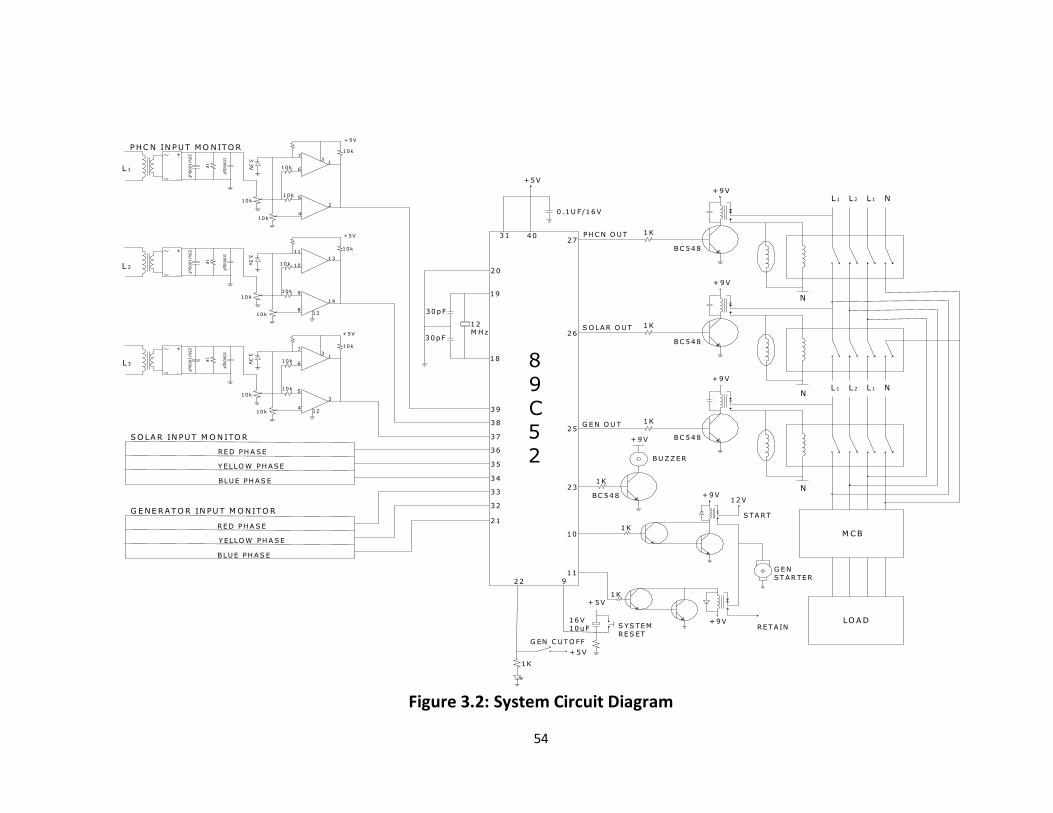
54
+
-
+
-
+
-
G
S O LA R IN PUT M O N ITO R
G E NE RA TO R IN PUT M O NITO R
RED PH A SE
Y ELLO W PH ASE
BLUE PH AS E
RED PH A SE
Y ELLO W PH A SE
BLUE PH AS E
P HC N IN P UT M O NITO R
L 1
L 2
L 3 89C52
PH C N O UT
S O LAR O UT
G EN O U T
BU ZZER
G ENST AR TER
S TA RT
RET AINS YS TEMRES ET
LO A D
M CB
N
N
N
+ 9V
+ 9V
+ 9V
+ 9V
+ 9V12V
+ 9V
+ 5V
+ 5V
+5V
+ 5V
+5V
+ 5V
30pF
12M H z
30pF
0 .1U F/16V
L1 N
137
1113
14
12
12
7
6
5
4
1
2
3
31 40 27
26
25
23
10
11922
21
32
33
34
35
36
37
38
39
18
19
20
6
5
4
2
10
9
8
L 2 L 1
L 1 NL2 L 1
10k
10k
10k
10k
3.3V
1 0k
10k
10k10k
3.3v
1 0k
10k
10k
3.3V
1 0k
10k
10k
10k
1K
1K
1K
1K
1K
1K
1K
25V/1000uF
1K
10000pF
25V/1000uF
1K
10000pF
25V/1000uF
1K
10000pF
B C 548
BC 548
BC 548
BC 548
16V10uF
G EN C UT O FF
Figure 3.2: System Circuit Diagram

55
Materials and technical information for this work was gathered from textbooks,
data books, the internet as well as staff of experienced companies such as
JohnHolt Engineering and Enugu Electricity Distribution Company (EEDC).
3.1 Design Stages: Circuit Simulation
To achieve the design, the circuit was first simulated using PROTEUS. PROTEUS is
a software for microprocessor simulation, schematic capture and PCB (Printed
Circuit Board) design. The simulation of the project was just as important as the
hardware implementation. It helped in observing and understanding the function
of the key circuits in detail before the hardware implementation. The circuit
simulation dealt with observing the response of the different components that
make up the design, checking the output of various indicators before
implementing into hardware. All the desired functionality was observed to be
working using PROTEUS simulation software.
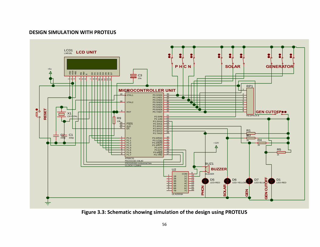
56
DESIGN SIMULATION WITH PROTEUS
Figure 3.3: Schematic showing simulation of the design using PROTEUS
XTAL218
XTAL119
ALE30
EA31
PSEN29
RST9
P0.0/AD0 39
P0.1/AD1 38
P0.2/AD2 37
P0.3/AD3 36
P0.4/AD4 35
P0.5/AD5 34
P0.6/AD6 33
P0.7/AD7 32
P1.01
P1.12
P1.23
P1.34
P1.45
P1.56
P1.67
P1.78
P3.0/RXD 10
P3.1/TXD 11
P3.2/INT0 12
P3.3/INT1 13
P3.4/T0 14
P3.7/RD 17P3.6/WR 16P3.5/T1 15
P2.7/A15 28
P2.0/A8 21
P2.1/A9 22
P2.2/A10 23
P2.3/A11 24
P2.4/A12 25
P2.5/A13 26
P2.6/A14 27
U1
AT89C51PACKAGE=DIL40PROGRAM=industrial.hexCLOCK=12MHz
+5v
D7
14D
613
D5
12D
411
D3
10D
29
D1
8D
07
E6
RW5
RS
4
VSS
1
VD
D2
VEE
3
LCD1LM016L
D1LED-RED
+12V
X1CRYSTAL
C1330p
C2330p
C310u
R910k
D5LED-RED
D6LED-YELLOW
D7LED-BLUE
23456789
1RP1
RESPACK-8
1B1 1C 16
2B2 2C 15
3B3 3C 14
4B4 4C 13
5B5 5C 12
6B6 6C 11
7B7 7C 10
COM 9U2
ULN2003A
BUZ1
BUZZER
R11kR31k R4
1k
R51k
LCD UNIT
MICROCONTROLLER UNIT
P H C N SOLAR GENERATOR
GEN CUTOFF
PHCN
SOLA
R
GEN
GEN
CUT
OFF
BUZZER
RES
ET
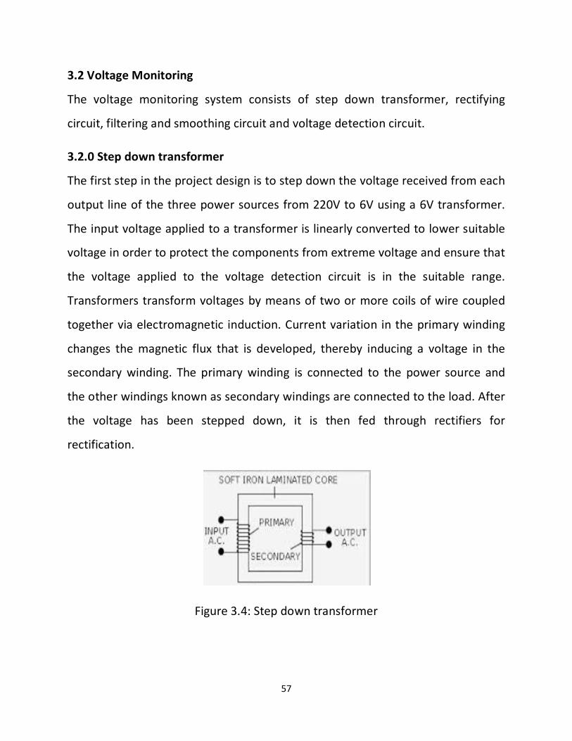
57
3.2 Voltage Monitoring
The voltage monitoring system consists of step down transformer, rectifying
circuit, filtering and smoothing circuit and voltage detection circuit.
3.2.0 Step down transformer
The first step in the project design is to step down the voltage received from each
output line of the three power sources from 220V to 6V using a 6V transformer.
The input voltage applied to a transformer is linearly converted to lower suitable
voltage in order to protect the components from extreme voltage and ensure that
the voltage applied to the voltage detection circuit is in the suitable range.
Transformers transform voltages by means of two or more coils of wire coupled
together via electromagnetic induction. Current variation in the primary winding
changes the magnetic flux that is developed, thereby inducing a voltage in the
secondary winding. The primary winding is connected to the power source and
the other windings known as secondary windings are connected to the load. After
the voltage has been stepped down, it is then fed through rectifiers for
rectification.
Figure 3.4: Step down transformer
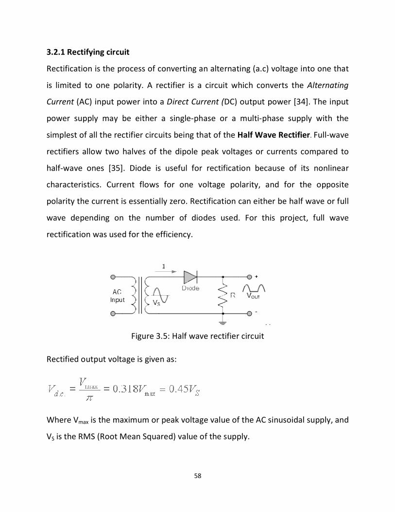
58
3.2.1 Rectifying circuit
Rectification is the process of converting an alternating (a.c) voltage into one that
is limited to one polarity. A rectifier is a circuit which converts the Alternating
Current (AC) input power into a Direct Current (DC) output power [34]. The input
power supply may be either a single-phase or a multi-phase supply with the
simplest of all the rectifier circuits being that of the Half Wave Rectifier. Full-wave
rectifiers allow two halves of the dipole peak voltages or currents compared to
half-wave ones [35]. Diode is useful for rectification because of its nonlinear
characteristics. Current flows for one voltage polarity, and for the opposite
polarity the current is essentially zero. Rectification can either be half wave or full
wave depending on the number of diodes used. For this project, full wave
rectification was used for the efficiency.
Figure 3.5: Half wave rectifier circuit
Rectified output voltage is given as:
Where Vmax is the maximum or peak voltage value of the AC sinusoidal supply, and
VS is the RMS (Root Mean Squared) value of the supply.
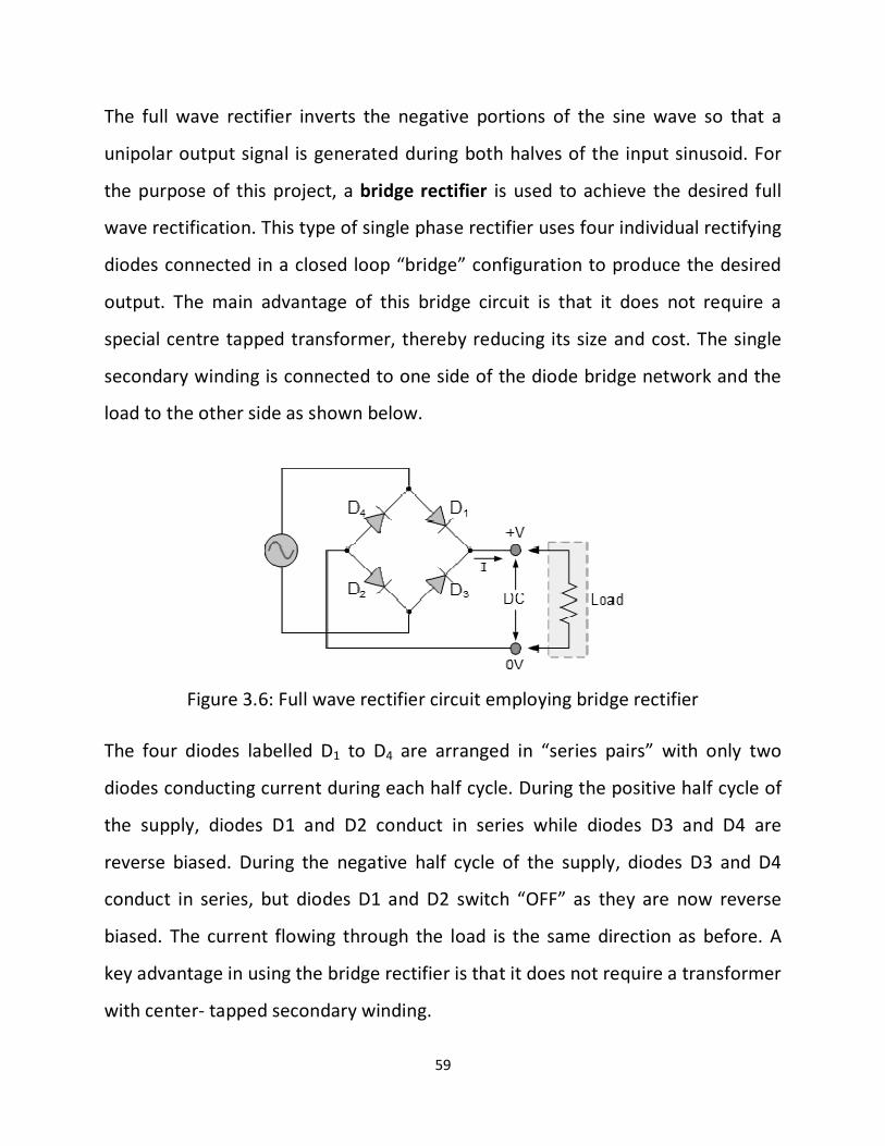
59
The full wave rectifier inverts the negative portions of the sine wave so that a
unipolar output signal is generated during both halves of the input sinusoid. For
the purpose of this project, a bridge rectifier is used to achieve the desired full
wave rectification. This type of single phase rectifier uses four individual rectifying
diodes connected in a closed loop “bridge” configuration to produce the desired
output. The main advantage of this bridge circuit is that it does not require a
special centre tapped transformer, thereby reducing its size and cost. The single
secondary winding is connected to one side of the diode bridge network and the
load to the other side as shown below.
Figure 3.6: Full wave rectifier circuit employing bridge rectifier
The four diodes labelled D1 to D4 are arranged in “series pairs” with only two
diodes conducting current during each half cycle. During the positive half cycle of
the supply, diodes D1 and D2 conduct in series while diodes D3 and D4 are
reverse biased. During the negative half cycle of the supply, diodes D3 and D4
conduct in series, but diodes D1 and D2 switch “OFF” as they are now reverse
biased. The current flowing through the load is the same direction as before. A
key advantage in using the bridge rectifier is that it does not require a transformer
with center- tapped secondary winding.
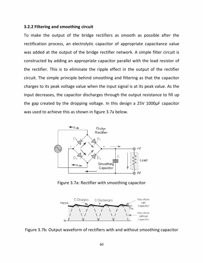
60
3.2.2 Filtering and smoothing circuit
To make the output of the bridge rectifiers as smooth as possible after the
rectification process, an electrolytic capacitor of appropriate capacitance value
was added at the output of the bridge rectifier network. A simple filter circuit is
constructed by adding an appropriate capacitor parallel with the load resistor of
the rectifier. This is to eliminate the ripple effect in the output of the rectifier
circuit. The simple principle behind smoothing and filtering as that the capacitor
charges to its peak voltage value when the input signal is at its peak value. As the
input decreases, the capacitor discharges through the output resistance to fill up
the gap created by the dropping voltage. In this design a 25V 1000µF capacitor
was used to achieve this as shown in figure 3.7a below.
Figure 3.7a: Rectifier with smoothing capacitor
Figure 3.7b: Output waveform of rectifiers with and without smoothing capacitor

61
The smoothing capacitor converts the full-wave rippled output of the rectifier into
a smooth DC output voltage. Generally for DC power supply circuits the
smoothing capacitor is an Aluminium Electrolytic type that has a capacitance
value of 100µF or more with repeated DC voltage pulses from the rectifier
charging up the capacitor to peak voltage. There are two important parameters to
consider when choosing a suitable smoothing capacitor and these are its working
voltage, which must be higher than the no-load output value of the rectifier and
its capacitance value, which determines the amount of ripple that will appear
superimposed on top of the DC voltage.
Too low a capacitance value will have little effect on the output waveform. But if
the smoothing capacitor is sufficiently large and the load current is not too large,
the output voltage will be almost as smooth as pure DC. A general rule is to have
a ripple voltage of less than 100mV peak to peak.
The maximum ripple voltage present for a Full Wave Rectifier circuit is not only
determined by the value of the smoothing capacitor but by the frequency and
load current, and is calculated as:
Vripple=Iload ×
,
Where I is the DC load current in amps, ƒ is the frequency of the ripple or twice
the input frequency in Hertz, and C is the capacitance in Farads.
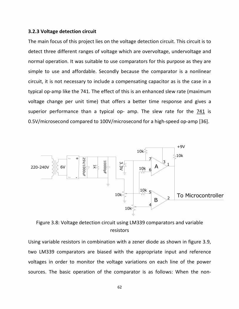
62
3.2.3 Voltage detection circuit
The main focus of this project lies on the voltage detection circuit. This circuit is to
detect three different ranges of voltage which are overvoltage, undervoltage and
normal operation. It was suitable to use comparators for this purpose as they are
simple to use and affordable. Secondly because the comparator is a nonlinear
circuit, it is not necessary to include a compensating capacitor as is the case in a
typical op-amp like the 741. The effect of this is an enhanced slew rate (maximum
voltage change per unit time) that offers a better time response and gives a
superior performance than a typical op- amp. The slew rate for the 741 is
0.5V/microsecond compared to 100V/microsecond for a high-speed op-amp [36].
+
-
220-240V
+9V
137
6
5
4
2
10k
10k
10k
10k
3.3V
10k
6V
To Microcontroller
25V/1000uF
1K
10000pF
10k
A
B
Figure 3.8: Voltage detection circuit using LM339 comparators and variable resistors
Using variable resistors in combination with a zener diode as shown in figure 3.9,
two LM339 comparators are biased with the appropriate input and reference
voltages in order to monitor the voltage variations on each line of the power
sources. The basic operation of the comparator is as follows: When the non-
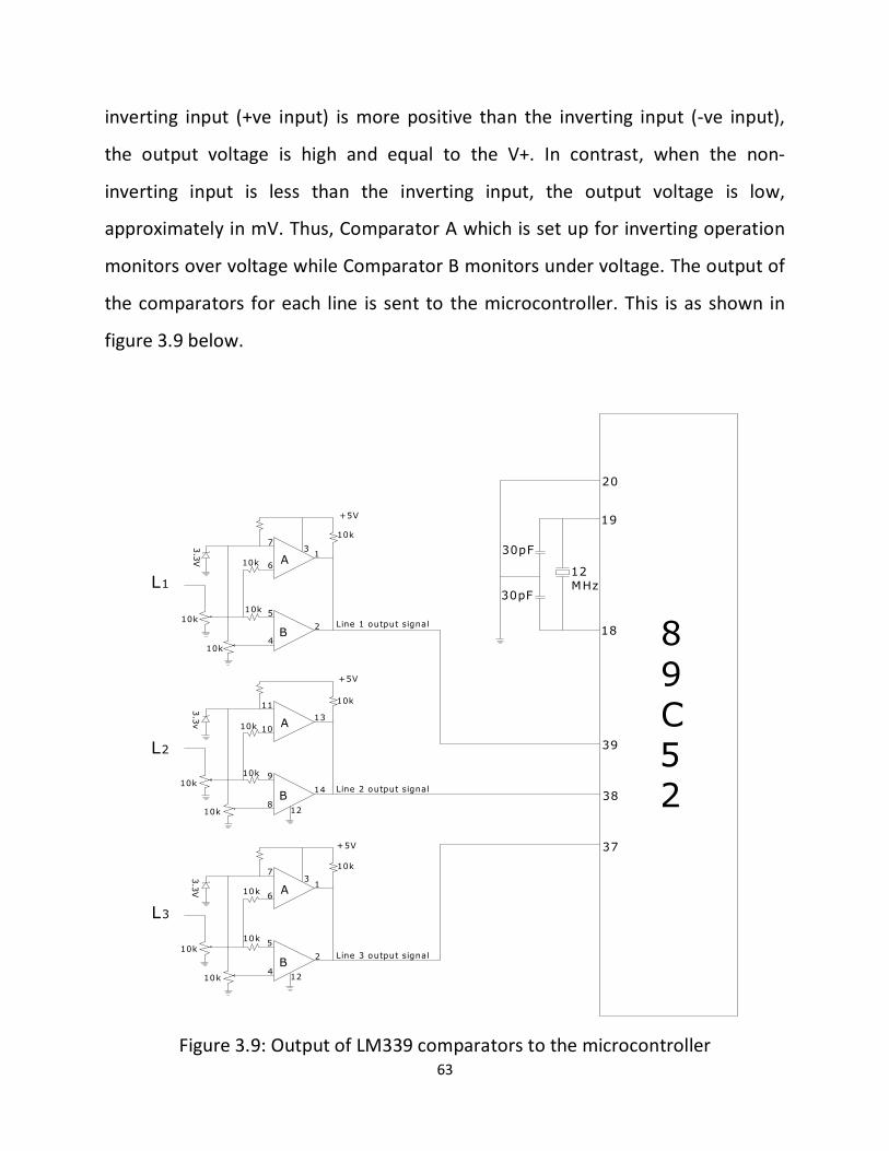
63
inverting input (+ve input) is more positive than the inverting input (-ve input),
the output voltage is high and equal to the V+. In contrast, when the non-
inverting input is less than the inverting input, the output voltage is low,
approximately in mV. Thus, Comparator A which is set up for inverting operation
monitors over voltage while Comparator B monitors under voltage. The output of
the comparators for each line is sent to the microcontroller. This is as shown in
figure 3.9 below.
89C52
+5V
+5V
+5V
30pF
12MHz
30pF
137
1113
14
12
12
7
6
5
4
1
2
3
18
19
20
6
5
4
2
10
9
8
10k
10k
10k
10k
3.3V
10k
10k
10k10k
3.3v10k
10k
10k
3.3V
10k
10k
10k
10k
38
39
37
L1
L2
L3
B
A
A
B
A
B
Line 1 output signal
Line 2 output signal
Line 3 output signal
Figure 3.9: Output of LM339 comparators to the microcontroller
64
Under normal conditions at the output of the power sources, the comparator
output will be HIGH, so the microcontroller assumes abnormality anytime it
senses a LOW at the output of the comparators.
3.3 Realizing the Software
The software program for this project was written with 8051 Assembly language
program using the 8051 instruction set. An Assembly language program is a series
of statements, or lines, which are either assembly language instructions such as
ADD and MOV, or statements called derivatives [37]. The instruction set of a
microcontroller is a set of instructions recognized by the microcontroller. The
instruction set of the 8051 microcontroller is shown in appendix B.
The software for this project work was written in modular form. Subroutines were
extensively used to achieve most of the desired functionality. Each subroutine
served a particular function, for instance the delay subroutine will delay the
microcontroller for an interval. The aim achieved through the use of subroutines
was that it made the program concise compared to the functionality.
Once the system is powered up the microcontroller configures the port pins.
Some pins will be configured as input pins and some as output pins. Port 0 of the
microcontroller was used as input port for the output of the comparators
monitoring the power sources. Once the microcontroller is done with initializing,
it starts sampling the signals from the power sources beginning with the PHCN
line. The software code that drives the system is shown in appendix C.
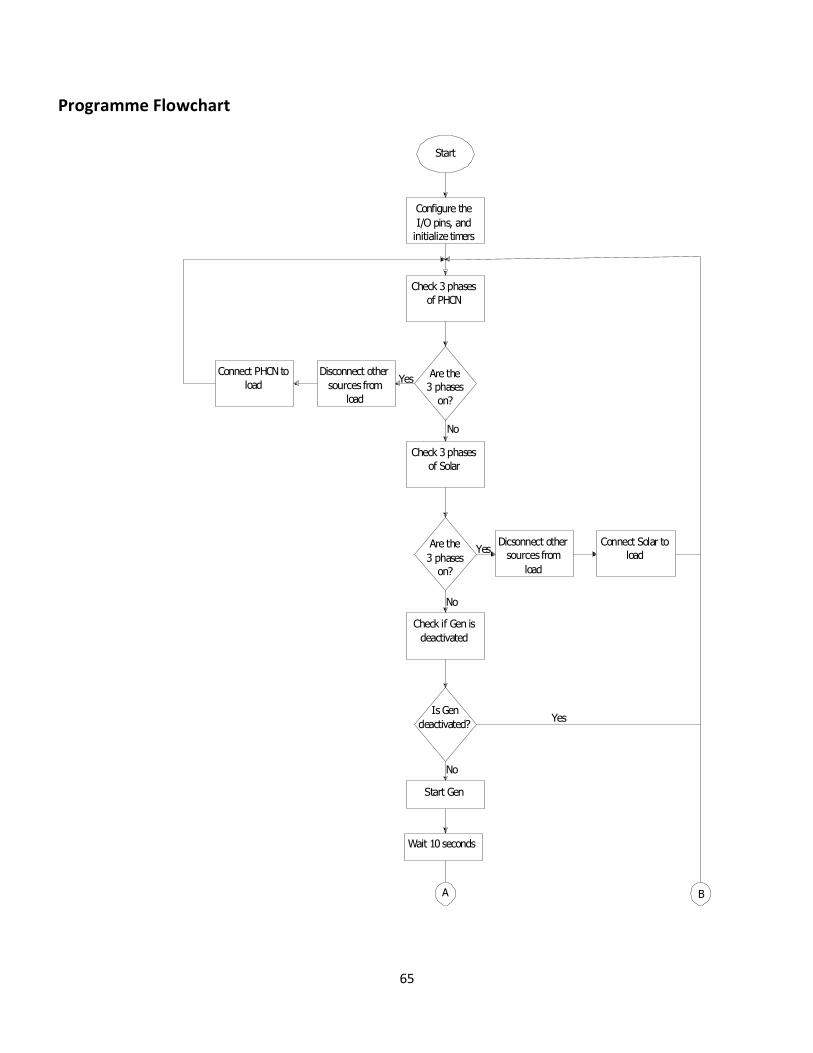
65
Start
Configure theI/O pins, and
initialize timers
Check 3 phasesof PHCN
Are the3 phases
on?
Disconnect othersources from
load
Connect PHCN toload
Check 3 phasesof Solar
Are the3 phases
on?
Connect Solar toload
Dicsonnect othersources from
load
Yes
Yes
No
Check if Gen isdeactivated
Is Gendeactivated?
No
Yes
Start Gen
Wait 10 seconds
No
A B
Programme Flowchart
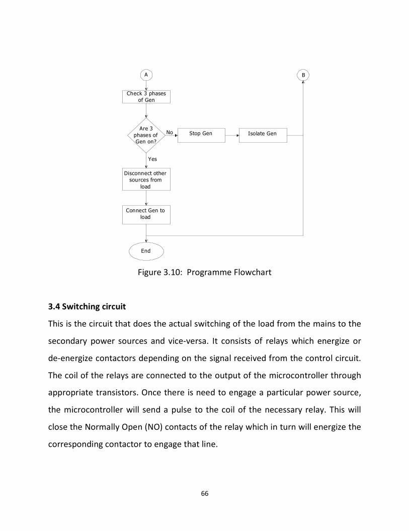
66
End
Disconnect othersources from
load
Connect Gen toload
Isolate GenStop GenAre 3
phases ofGen on?
Check 3 phasesof Gen
A B
Yes
No
Figure 3.10: Programme Flowchart
3.4 Switching circuit
This is the circuit that does the actual switching of the load from the mains to the
secondary power sources and vice-versa. It consists of relays which energize or
de-energize contactors depending on the signal received from the control circuit.
The coil of the relays are connected to the output of the microcontroller through
appropriate transistors. Once there is need to engage a particular power source,
the microcontroller will send a pulse to the coil of the necessary relay. This will
close the Normally Open (NO) contacts of the relay which in turn will energize the
corresponding contactor to engage that line.
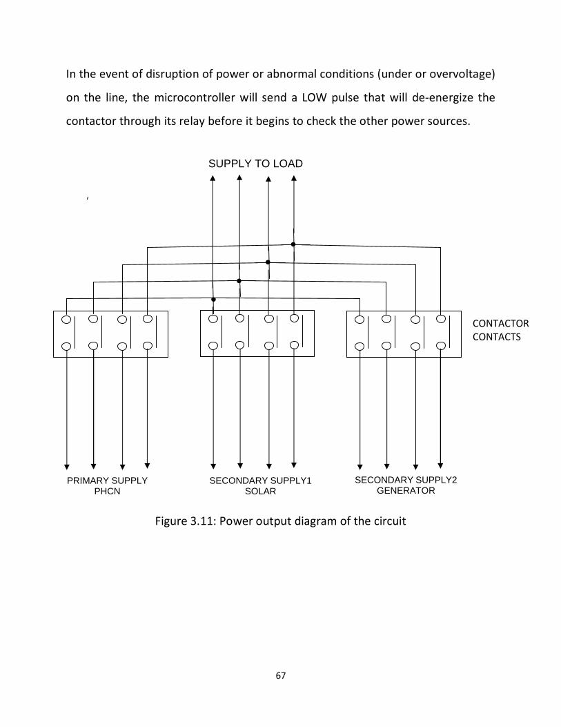
67
In the event of disruption of power or abnormal conditions (under or overvoltage)
on the line, the microcontroller will send a LOW pulse that will de-energize the
contactor through its relay before it begins to check the other power sources.
Figure 3.11: Power output diagram of the circuit
•
•
•
•
SUPPLY TO LOAD
SECONDARY SUPPLY1 SOLAR
SECONDARY SUPPLY2 GENERATOR
PRIMARY SUPPLY PHCN
CONTACTOR CONTACTS
68
CHAPTER FOUR
SYSTEM DESIGN AND IMPLEMENTATION
4.0 Selection Of Components
The system is intended to handle a load of 20KVA.
Therefore using the power equation for a 3 phase supply;
= √3Ɵ ……………………………..……………………….. Equation 4.1
Where;
V = Line Voltage = 415V
I = Full Load Current
CosƟ = Power Factor = 0.8
P = 20KVA
Therefore full load current,
I = √Ɵ
…………………………………………………..…. Equation 4.2
Assuming power factor of 0.8
I = √× × .
= 34.78A
Therefore current capacity of system at full load = 34.78 amps
4.1 Contactor Design
In choosing the contactors the full load current was considered. From calculations
the full load current was 34.78 A. Therefore contactors must be rated above 35A.
For the purpose of this work, three 40A 4-pole (3 phase) contactors were used,
one for each of the three power sources.
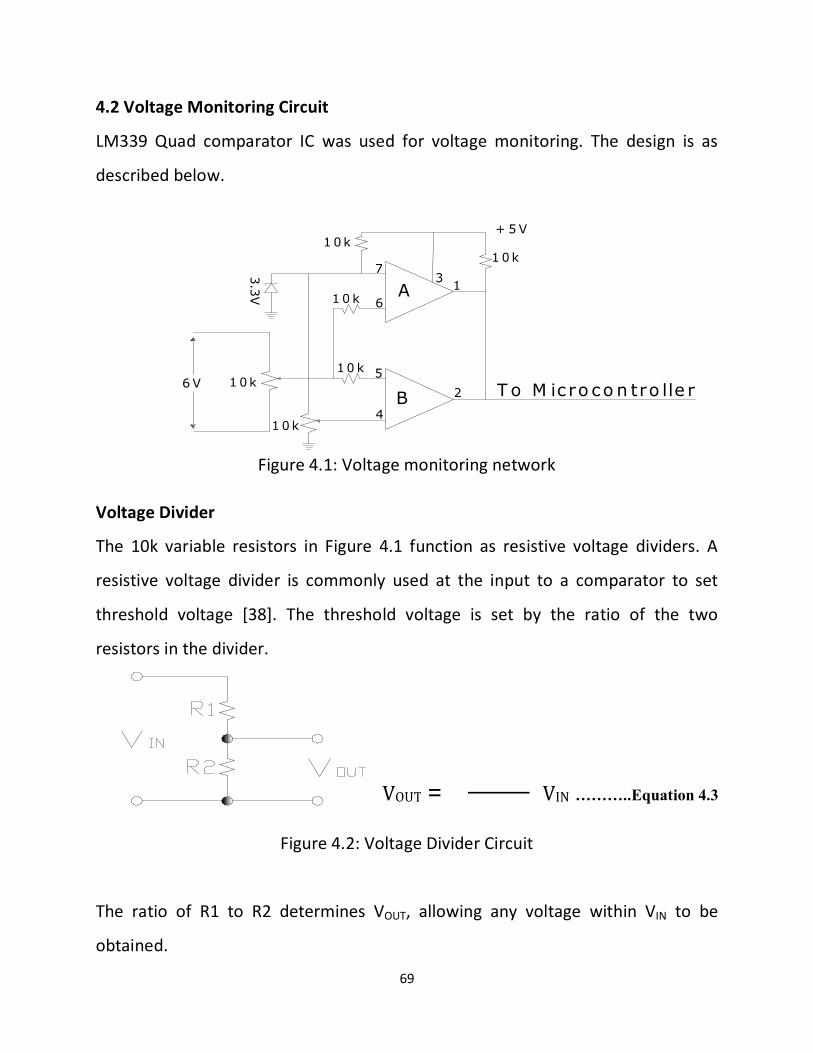
69
4.2 Voltage Monitoring Circuit
LM339 Quad comparator IC was used for voltage monitoring. The design is as
described below.
+ 5 V
137
6
5
4
2
1 0 k
10 k
1 0k
1 0k
3.3V
1 0 k
T o M ic ro co n tro lle r6 V
A
B
1 0k
Figure 4.1: Voltage monitoring network
Voltage Divider
The 10k variable resistors in Figure 4.1 function as resistive voltage dividers. A
resistive voltage divider is commonly used at the input to a comparator to set
threshold voltage [38]. The threshold voltage is set by the ratio of the two
resistors in the divider.
Figure 4.2: Voltage Divider Circuit
The ratio of R1 to R2 determines VOUT, allowing any voltage within VIN to be
obtained.
VOUT =
VIN ………..Equation 4.3
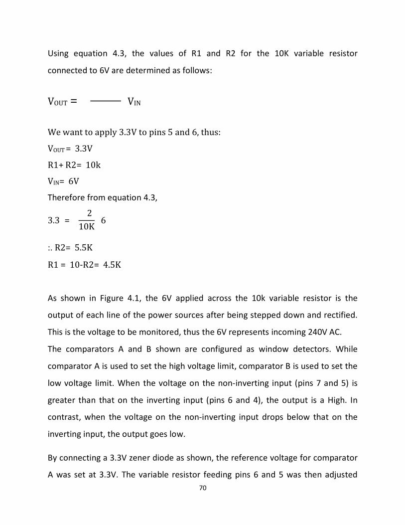
70
Using equation 4.3, the values of R1 and R2 for the 10K variable resistor
connected to 6V are determined as follows:
VOUT =
VIN
We want to apply 3.3V to pins 5 and 6, thus:
VOUT = 3.3V
R1+ R2= 10k
VIN= 6V
Therefore from equation 4.3,
3.3 = 2
10K6
:. R2= 5.5K
R1 = 10-R2= 4.5K
As shown in Figure 4.1, the 6V applied across the 10k variable resistor is the
output of each line of the power sources after being stepped down and rectified.
This is the voltage to be monitored, thus the 6V represents incoming 240V AC.
The comparators A and B shown are configured as window detectors. While
comparator A is used to set the high voltage limit, comparator B is used to set the
low voltage limit. When the voltage on the non-inverting input (pins 7 and 5) is
greater than that on the inverting input (pins 6 and 4), the output is a High. In
contrast, when the voltage on the non-inverting input drops below that on the
inverting input, the output goes low.
By connecting a 3.3V zener diode as shown, the reference voltage for comparator
A was set at 3.3V. The variable resistor feeding pins 6 and 5 was then adjusted
71
until 3.3V was gotten. The effect is that at 240 V, which is equivalent to 6V across
the 10k variable resistor, input pins 6 and 5 will see 3.3V. Therefore, when the
voltage exceeds 240V, input to pin 6 will exceed 3.3V which is the reference
voltage of comparator A, thus the output will go Low.
Then to set the low voltage limit (185V ac), transformer equation was first applied
to get the dc voltage equivalent of 185V:
=
…………………………………………………….……..…. Equation 4.4
Therefore,
=
= 40
Therefore,
= 40; y = 4.625V
Therefore at 185V ac, output voltage = 4.625V dc
By comparison, if 6V ≡ 3.3V
:. 4.625V ≡ .
× 4.625 = 2.5V
Thus at 185V, which is equivalent to 4.625V, input pins 6 and 5 will see 2.5V. This
is the low voltage reference to be applied to pin 4. So using equation 4.3 again,
the values of R1 and R2 for the 10K variable resistor connected to 3.3V are
determined as follows:
72
VOUT =
VIN
We want to apply 2.5V to pin 4, thus:
VOUT = 2.5V
R1+ R2= 10k
VIN= 3.3V
Therefore from equation 4.3,
2.5 = 2
10K3.3
:. R2= 7.6K
R1 = 10-R2= 2.4K
Therefore the 10K variable resistor attached to pin 4 was adjusted to obtain 2.5V,
which is the low voltage reference, such that when supply voltage drops below
185V, the voltage at input to pin 5 will drop below 2.5V, thus driving the output of
comparator B to a Low state. However, if the supply voltage falls within the
required range (185V to 240V ac) both comparator outputs will be high signifying
normal voltage supply.
The LM339 comparator has an open collector configuration, therefore the 10K
resistor attached to the output is a pullup resistor ensuring that the output is
pulled up to +5V that the microcontroller can sense. In this way the
microcontroller monitors the output of the power sources.
4.3 Circuit Breaker Design
In order to avoid loading the system beyond its capacity, considering full load
current of 34.78 Amps, a 30 Amps 4 pole (3-phase) circuit breaker will be used.
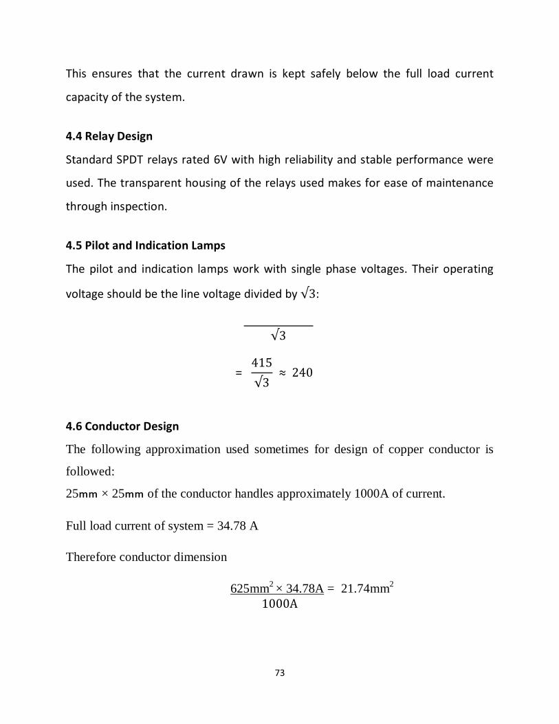
73
This ensures that the current drawn is kept safely below the full load current
capacity of the system.
4.4 Relay Design
Standard SPDT relays rated 6V with high reliability and stable performance were
used. The transparent housing of the relays used makes for ease of maintenance
through inspection.
4.5 Pilot and Indication Lamps
The pilot and indication lamps work with single phase voltages. Their operating
voltage should be the line voltage divided by √3:
√3
= 415√3
≈ 240
4.6 Conductor Design
The following approximation used sometimes for design of copper conductor is
followed:
25mm × 25mm of the conductor handles approximately 1000A of current.
Full load current of system = 34.78 A
Therefore conductor dimension
625mm2 × 34.78A = 21.74mm2 1000A
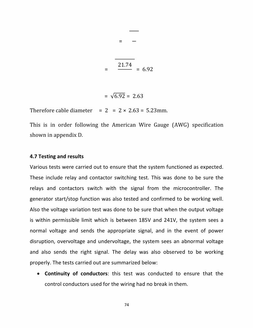
74
=
= 21.74
= 6.92
= √6.92 = 2.63
Therefore cable diameter = 2 = 2 × 2.63 = 5.23mm.
This is in order following the American Wire Gauge (AWG) specification
shown in appendix D.
4.7 Testing and results
Various tests were carried out to ensure that the system functioned as expected.
These include relay and contactor switching test. This was done to be sure the
relays and contactors switch with the signal from the microcontroller. The
generator start/stop function was also tested and confirmed to be working well.
Also the voltage variation test was done to be sure that when the output voltage
is within permissible limit which is between 185V and 241V, the system sees a
normal voltage and sends the appropriate signal, and in the event of power
disruption, overvoltage and undervoltage, the system sees an abnormal voltage
and also sends the right signal. The delay was also observed to be working
properly. The tests carried out are summarized below:
• Continuity of conductors: this test was conducted to ensure that the
control conductors used for the wiring had no break in them.
75
• Continuity of normally closed contacts: the normally closed contacts gave
continuous reading when tested to indicate a closed contact. When
manually operated a discontinuous reading was attained to indicate
opened contact.
• Continuity of protective devices: all the protective devices where tested by
closing the contacts and using continuity tester to test for continuity. When
the protective devices such as the three phase line controller were closed,
the instrument gave a continuous signal indicating closed contacts,
meaning the electrical device is in good working condition.
• Operation of contactors, relays, timers, protective devices and interlocks:
the contactors, relays and the timers were energized to observe their
opening and breaking operation. They were found to be in good working
condition.
• Polarity checks: this was done to ensure that live and neutral polarity was
connected to the respective terminal block to prevent electrical hazards.
• Protection by electrical separation: this test was carried out by isolating
the breakers/switches and then tested to observe if there were leakages.
All the components were found to be in good working condition and the
control system performed satisfactorily.
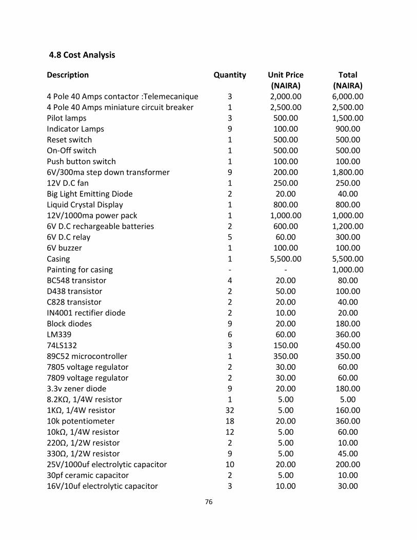
76
4.8 Cost Analysis
Description
Quantity
Unit Price (NAIRA)
Total (NAIRA)
4 Pole 40 Amps contactor :Telemecanique 3 2,000.00 6,000.00 4 Pole 40 Amps miniature circuit breaker 1 2,500.00 2,500.00 Pilot lamps 3 500.00 1,500.00 Indicator Lamps 9 100.00 900.00 Reset switch 1 500.00 500.00 On-Off switch 1 500.00 500.00 Push button switch 1 100.00 100.00 6V/300ma step down transformer 9 200.00 1,800.00 12V D.C fan 1 250.00 250.00 Big Light Emitting Diode 2 20.00 40.00 Liquid Crystal Display 1 800.00 800.00 12V/1000ma power pack 1 1,000.00 1,000.00 6V D.C rechargeable batteries 2 600.00 1,200.00 6V D.C relay 5 60.00 300.00 6V buzzer 1 100.00 100.00 Casing 1 5,500.00 5,500.00 Painting for casing - - 1,000.00 BC548 transistor 4 20.00 80.00 D438 transistor 2 50.00 100.00 C828 transistor 2 20.00 40.00 IN4001 rectifier diode 2 10.00 20.00 Block diodes 9 20.00 180.00 LM339 6 60.00 360.00 74LS132 3 150.00 450.00 89C52 microcontroller 1 350.00 350.00 7805 voltage regulator 2 30.00 60.00 7809 voltage regulator 2 30.00 60.00 3.3v zener diode 9 20.00 180.00 8.2KΩ, 1/4W resistor 1 5.00 5.00 1KΩ, 1/4W resistor 32 5.00 160.00 10k potentiometer 18 20.00 360.00 10kΩ, 1/4W resistor 12 5.00 60.00 220Ω, 1/2W resistor 2 5.00 10.00 330Ω, 1/2W resistor 9 5.00 45.00 25V/1000uf electrolytic capacitor 10 20.00 200.00 30pf ceramic capacitor 2 5.00 10.00 16V/10uf electrolytic capacitor 3 10.00 30.00
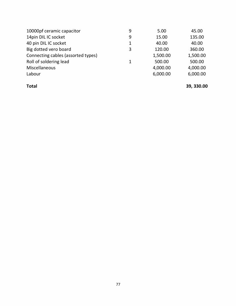
77
10000pf ceramic capacitor 9 5.00 45.00 14pin DIL IC socket 9 15.00 135.00 40 pin DIL IC socket 1 40.00 40.00 Big dotted vero board 3 120.00 360.00 Connecting cables (assorted types) 1,500.00 1,500.00 Roll of soldering lead 1 500.00 500.00 Miscellaneous 4,000.00 4,000.00 Labour 6,000.00 6,000.00 Total 39, 330.00

78
CHAPTER FIVE
CONCLUSION AND RECOMMENDATION
5.0 Conclusion
This project provides a means of cushioning the consequences of unreliable
power supply that pervade developing societies like Nigeria by offering a cost
effective way of using multitier power supplies. Owing to the fact that modern
industrial systems depend on regular supply of electricity, and quality of life as
well as standard of living today depend much on electricity, this project is very
relevant in our society today.
5.1 Recommendation
This device is recommended for use in homes, industries and facilities where
power supply from the grid is unreliable, and uninterrupted 3 phase power supply
is essential. Further, based on the experience gathered in the course of the
design, the following recommendations are suggested:
1. The machine should be made more robust, efficient and exportable by
using PCB (Printed Circuit Board) technology to develop the electronics
control board.
2. As an improvement the system can include a computer interface that will
link it to a Wide Area Network to facilitate advanced features like data
logging and remote sensing.
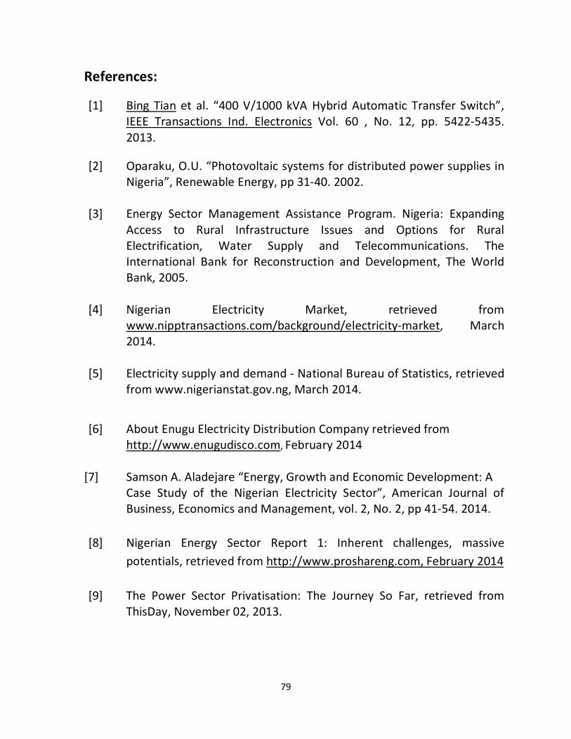
79
References:
[1] Bing Tian et al. “400 V/1000 kVA Hybrid Automatic Transfer Switch”, IEEE Transactions Ind. Electronics Vol. 60 , No. 12, pp. 5422-5435. 2013.
[2] Oparaku, O.U. “Photovoltaic systems for distributed power supplies in
Nigeria”, Renewable Energy, pp 31-40. 2002. [3] Energy Sector Management Assistance Program. Nigeria: Expanding
Access to Rural Infrastructure Issues and Options for Rural Electrification, Water Supply and Telecommunications. The International Bank for Reconstruction and Development, The World Bank, 2005.
[4] Nigerian Electricity Market, retrieved from
www.nipptransactions.com/background/electricity-market, March 2014.
[5] Electricity supply and demand - National Bureau of Statistics, retrieved
from www.nigerianstat.gov.ng, March 2014.
[6] About Enugu Electricity Distribution Company retrieved from http://www.enugudisco.com, February 2014
[7] Samson A. Aladejare “Energy, Growth and Economic Development: A
Case Study of the Nigerian Electricity Sector”, American Journal of Business, Economics and Management, vol. 2, No. 2, pp 41-54. 2014.
[8] Nigerian Energy Sector Report 1: Inherent challenges, massive
potentials, retrieved from http://www.proshareng.com, February 2014 [9] The Power Sector Privatisation: The Journey So Far, retrieved from
ThisDay, November 02, 2013.

80
[10] Nigeria: Electric Power Sector Reform 2013, Olivia Phillip International Consulting Limited, June 2013.
[11] How Effective Is Regulatory Intervention In Post-Privatised PHCN,
retrieved from, Leadership, February 23, 2014. [12] Confusion After Power Holding Company of Nigeria Privatisation,
retrieved from Eagle Reporters, December 04, 2013. [13] Transmission, generation challenges slow Discos’ investment drive,
retrieved from BusinessDay, January 16, 2014. [14] Promise U. Chukwu et al “Sustainable Energy Future for Nigeria: The
Role of Engineers” Journal of Sustainable Development Studies, vol. 6, No. 2, pp 242-259. 2014.
[15] Nigeria’s power generation capacity, retrieved from Premium Times,
March 30, 2014. [16] Emevon, I et al. Conference paper on “Power Generation in Nigeria;
Problem and Solution” retrieved from http://www.naee.org.ng/files/paper1.pdf, February 2015.
[17] Energy in Nigeria, retrieved from,
http//:en.wikipedia.org/wiki/Energy_in_Nigeria, August 2015.
[18] Nigeria Electricity-production, retrieved from, http://www.indexmundi.com, March 2014
[19] Population total, retrieved from
http://data.worldbank.org/indicator/SP.POP.TOTL, March 2014.
[20] O. U. Oparaku, “Solar-Photovoltaics In The Deregulated Electricity Industry Of Developing Countries”, Proceedings of the International Conference on Renewable Energy for Developing Countries, National Centre for Energy Research and Development, University of Nigeria, Nsukka, 2006.
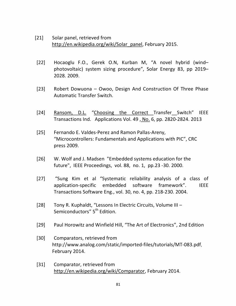
81
[21] Solar panel, retrieved from
http://en.wikipedia.org/wiki/Solar_panel, February 2015.
[22] Hocaoglu F.O., Gerek O.N, Kurban M, “A novel hybrid (wind–
photovoltaic) system sizing procedure”, Solar Energy 83, pp 2019–2028. 2009.
[23] Robert Dowuona – Owoo, Design And Construction Of Three Phase
Automatic Transfer Switch.
[24] Ransom, D.L. “Choosing the Correct Transfer Switch” IEEE Transactions Ind. Applications Vol. 49 , No. 6, pp. 2820-2824. 2013
[25] Fernando E. Valdes-Perez and Ramon Pallas-Areny,
“Microcontrollers: Fundamentals and Applications with PIC”, CRC press 2009.
[26] W. Wolf and J. Madsen "Embedded systems education for the
future", IEEE Proceedings, vol. 88, no. 1, pp.23 -30. 2000.
[27] “Sung Kim et al “Systematic reliability analysis of a class of application-specific embedded software framework”. IEEE Transactions Software Eng., vol. 30, no. 4, pp. 218-230. 2004.
[28] Tony R. Kuphaldt, “Lessons In Electric Circuits, Volume III – Semiconductors” 5th Edition.
[29] Paul Horowitz and Winfield Hill, “The Art of Electronics”, 2nd Edition
[30] Comparators, retrieved from http://www.analog.com/static/imported-files/tutorials/MT-083.pdf, February 2014.
[31] Comparator, retrieved from
http://en.wikipedia.org/wiki/Comparator, February 2014.
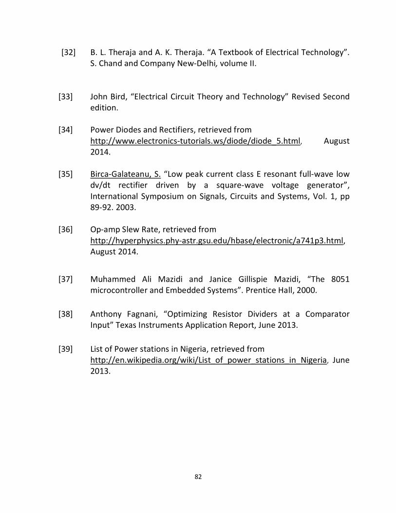
82
[32] B. L. Theraja and A. K. Theraja. “A Textbook of Electrical Technology”. S. Chand and Company New-Delhi, volume II.
[33] John Bird, “Electrical Circuit Theory and Technology” Revised Second edition.
[34] Power Diodes and Rectifiers, retrieved from
http://www.electronics-tutorials.ws/diode/diode_5.html, August 2014.
[35] Birca-Galateanu, S. “Low peak current class E resonant full-wave low
dv/dt rectifier driven by a square-wave voltage generator”, International Symposium on Signals, Circuits and Systems, Vol. 1, pp 89-92. 2003.
[36] Op-amp Slew Rate, retrieved from
http://hyperphysics.phy-astr.gsu.edu/hbase/electronic/a741p3.html, August 2014.
[37] Muhammed Ali Mazidi and Janice Gillispie Mazidi, “The 8051 microcontroller and Embedded Systems”. Prentice Hall, 2000.
[38] Anthony Fagnani, “Optimizing Resistor Dividers at a Comparator
Input” Texas Instruments Application Report, June 2013.
[39] List of Power stations in Nigeria, retrieved from http://en.wikipedia.org/wiki/List_of_power_stations_in_Nigeria, June 2013.
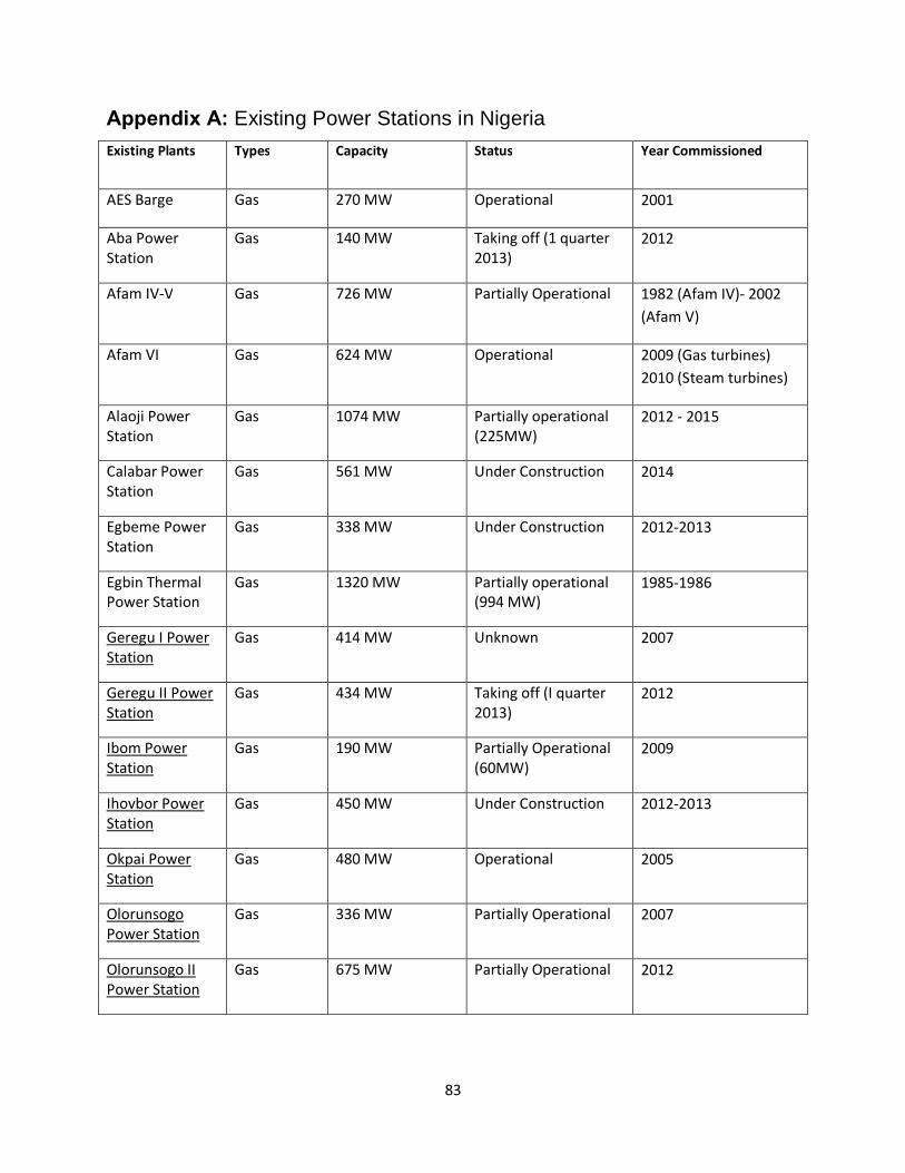
83
Appendix A: Existing Power Stations in Nigeria
Existing Plants Types Capacity Status Year Commissioned
AES Barge Gas 270 MW Operational 2001
Aba Power Station
Gas 140 MW Taking off (1 quarter 2013)
2012
Afam IV-V Gas 726 MW Partially Operational 1982 (Afam IV)- 2002 (Afam V)
Afam VI Gas 624 MW Operational 2009 (Gas turbines) 2010 (Steam turbines)
Alaoji Power Station
Gas 1074 MW Partially operational (225MW)
2012 - 2015
Calabar Power Station
Gas 561 MW Under Construction 2014
Egbeme Power Station
Gas 338 MW Under Construction 2012-2013
Egbin Thermal Power Station
Gas 1320 MW Partially operational (994 MW)
1985-1986
Geregu I Power Station
Gas 414 MW Unknown 2007
Geregu II Power Station
Gas 434 MW Taking off (I quarter 2013)
2012
Ibom Power Station
Gas 190 MW Partially Operational (60MW)
2009
Ihovbor Power Station
Gas 450 MW Under Construction 2012-2013
Okpai Power Station
Gas 480 MW Operational 2005
Olorunsogo Power Station
Gas 336 MW Partially Operational 2007
Olorunsogo II Power Station
Gas 675 MW Partially Operational 2012
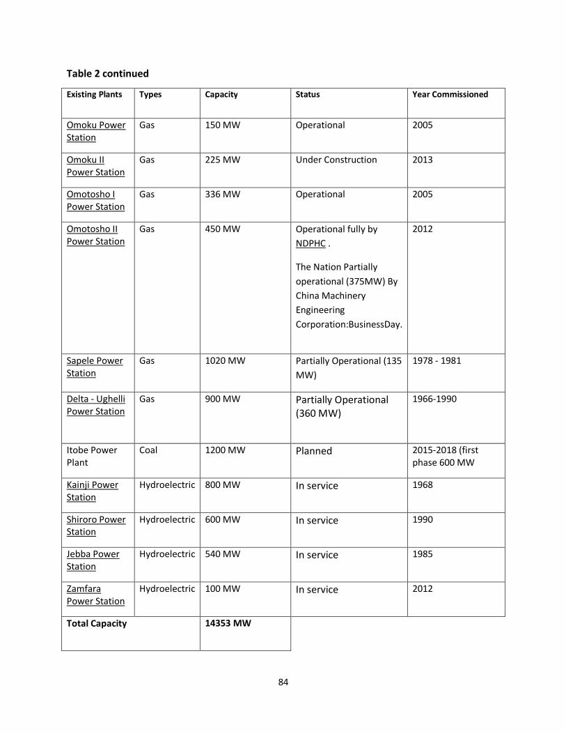
84
Table 2 continued
Existing Plants Types Capacity Status Year Commissioned
Omoku Power Station
Gas 150 MW Operational 2005
Omoku II Power Station
Gas 225 MW Under Construction 2013
Omotosho I Power Station
Gas 336 MW Operational 2005
Omotosho II Power Station
Gas 450 MW Operational fully by NDPHC .
The Nation Partially operational (375MW) By China Machinery Engineering Corporation:BusinessDay.
2012
Sapele Power Station
Gas 1020 MW Partially Operational (135 MW)
1978 - 1981
Delta - Ughelli Power Station
Gas 900 MW Partially Operational (360 MW)
1966-1990
Itobe Power Plant
Coal 1200 MW Planned 2015-2018 (first phase 600 MW
Kainji Power Station
Hydroelectric 800 MW In service 1968
Shiroro Power Station
Hydroelectric 600 MW In service 1990
Jebba Power Station
Hydroelectric 540 MW In service 1985
Zamfara Power Station
Hydroelectric 100 MW In service 2012
Total Capacity 14353 MW
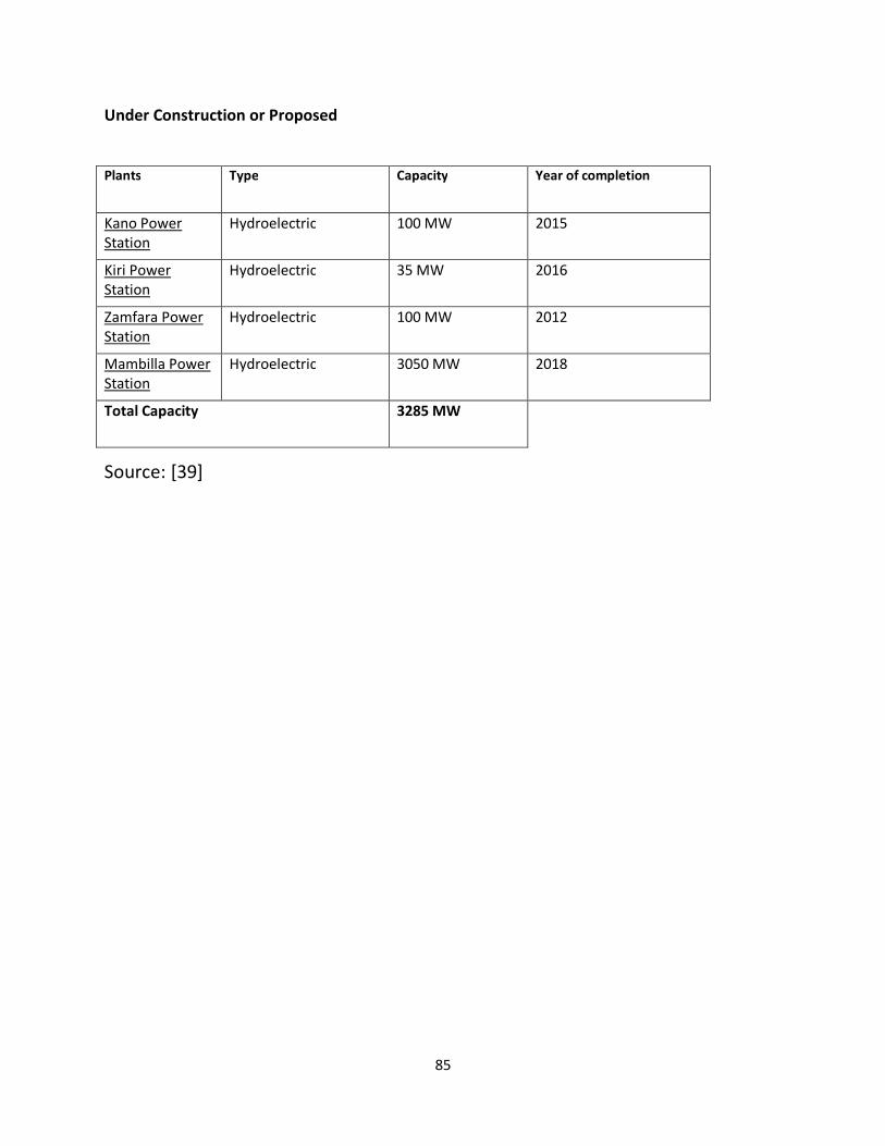
85
Under Construction or Proposed
Source: [39]
Plants Type Capacity Year of completion
Kano Power Station
Hydroelectric 100 MW 2015
Kiri Power Station
Hydroelectric 35 MW 2016
Zamfara Power Station
Hydroelectric 100 MW 2012
Mambilla Power Station
Hydroelectric 3050 MW 2018
Total Capacity 3285 MW
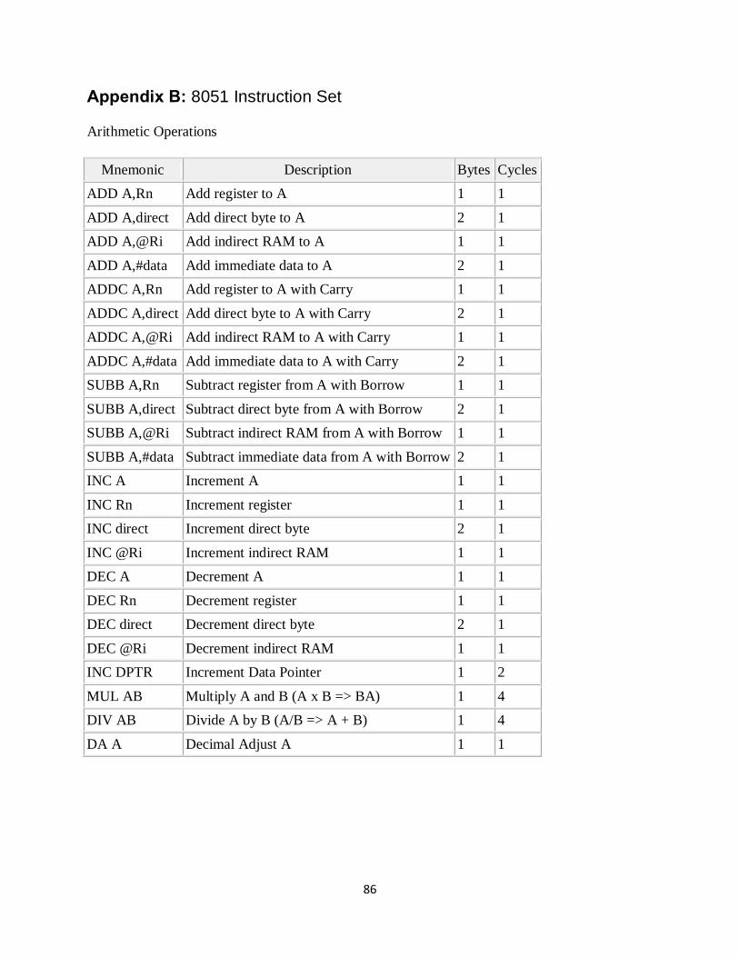
86
Appendix B: 8051 Instruction Set
Arithmetic Operations
Mnemonic Description Bytes Cycles ADD A,Rn Add register to A 1 1
ADD A,direct Add direct byte to A 2 1 ADD A,@Ri Add indirect RAM to A 1 1
ADD A,#data Add immediate data to A 2 1 ADDC A,Rn Add register to A with Carry 1 1
ADDC A,direct Add direct byte to A with Carry 2 1 ADDC A,@Ri Add indirect RAM to A with Carry 1 1
ADDC A,#data Add immediate data to A with Carry 2 1 SUBB A,Rn Subtract register from A with Borrow 1 1
SUBB A,direct Subtract direct byte from A with Borrow 2 1 SUBB A,@Ri Subtract indirect RAM from A with Borrow 1 1
SUBB A,#data Subtract immediate data from A with Borrow 2 1 INC A Increment A 1 1
INC Rn Increment register 1 1 INC direct Increment direct byte 2 1
INC @Ri Increment indirect RAM 1 1 DEC A Decrement A 1 1
DEC Rn Decrement register 1 1 DEC direct Decrement direct byte 2 1
DEC @Ri Decrement indirect RAM 1 1 INC DPTR Increment Data Pointer 1 2
MUL AB Multiply A and B (A x B => BA) 1 4 DIV AB Divide A by B (A/B => A + B) 1 4
DA A Decimal Adjust A 1 1
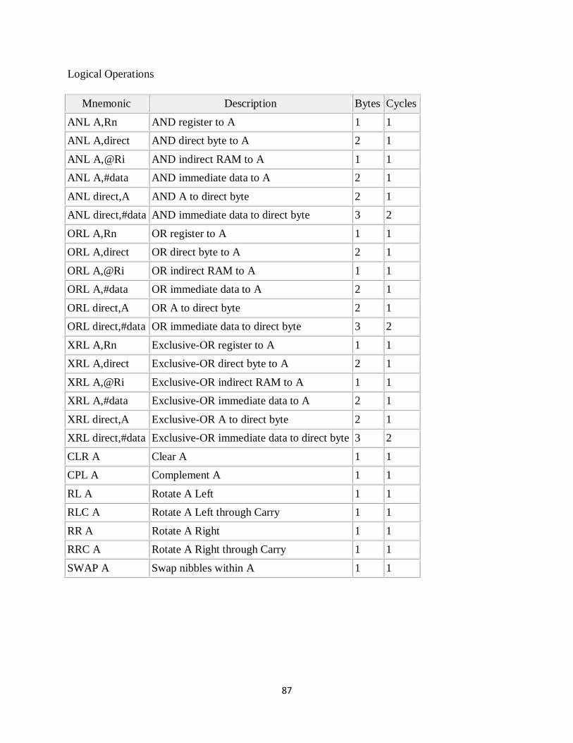
87
Logical Operations
Mnemonic Description Bytes Cycles
ANL A,Rn AND register to A 1 1 ANL A,direct AND direct byte to A 2 1
ANL A,@Ri AND indirect RAM to A 1 1 ANL A,#data AND immediate data to A 2 1
ANL direct,A AND A to direct byte 2 1 ANL direct,#data AND immediate data to direct byte 3 2
ORL A,Rn OR register to A 1 1 ORL A,direct OR direct byte to A 2 1
ORL A,@Ri OR indirect RAM to A 1 1 ORL A,#data OR immediate data to A 2 1
ORL direct,A OR A to direct byte 2 1 ORL direct,#data OR immediate data to direct byte 3 2
XRL A,Rn Exclusive-OR register to A 1 1 XRL A,direct Exclusive-OR direct byte to A 2 1
XRL A,@Ri Exclusive-OR indirect RAM to A 1 1 XRL A,#data Exclusive-OR immediate data to A 2 1
XRL direct,A Exclusive-OR A to direct byte 2 1 XRL direct,#data Exclusive-OR immediate data to direct byte 3 2
CLR A Clear A 1 1 CPL A Complement A 1 1
RL A Rotate A Left 1 1 RLC A Rotate A Left through Carry 1 1
RR A Rotate A Right 1 1 RRC A Rotate A Right through Carry 1 1
SWAP A Swap nibbles within A 1 1
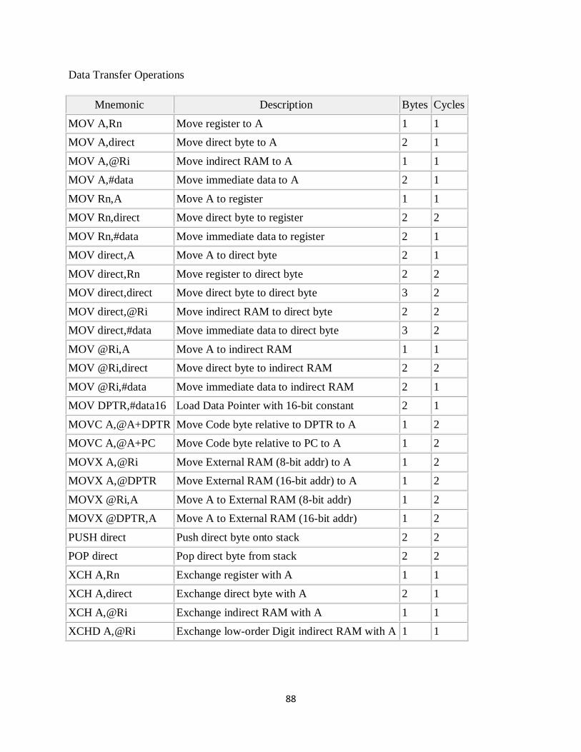
88
Data Transfer Operations
Mnemonic Description Bytes Cycles
MOV A,Rn Move register to A 1 1 MOV A,direct Move direct byte to A 2 1
MOV A,@Ri Move indirect RAM to A 1 1 MOV A,#data Move immediate data to A 2 1
MOV Rn,A Move A to register 1 1 MOV Rn,direct Move direct byte to register 2 2
MOV Rn,#data Move immediate data to register 2 1 MOV direct,A Move A to direct byte 2 1
MOV direct,Rn Move register to direct byte 2 2 MOV direct,direct Move direct byte to direct byte 3 2
MOV direct,@Ri Move indirect RAM to direct byte 2 2 MOV direct,#data Move immediate data to direct byte 3 2
MOV @Ri,A Move A to indirect RAM 1 1 MOV @Ri,direct Move direct byte to indirect RAM 2 2
MOV @Ri,#data Move immediate data to indirect RAM 2 1 MOV DPTR,#data16 Load Data Pointer with 16-bit constant 2 1
MOVC A,@A+DPTR Move Code byte relative to DPTR to A 1 2 MOVC A,@A+PC Move Code byte relative to PC to A 1 2
MOVX A,@Ri Move External RAM (8-bit addr) to A 1 2 MOVX A,@DPTR Move External RAM (16-bit addr) to A 1 2
MOVX @Ri,A Move A to External RAM (8-bit addr) 1 2 MOVX @DPTR,A Move A to External RAM (16-bit addr) 1 2
PUSH direct Push direct byte onto stack 2 2 POP direct Pop direct byte from stack 2 2
XCH A,Rn Exchange register with A 1 1 XCH A,direct Exchange direct byte with A 2 1
XCH A,@Ri Exchange indirect RAM with A 1 1 XCHD A,@Ri Exchange low-order Digit indirect RAM with A 1 1
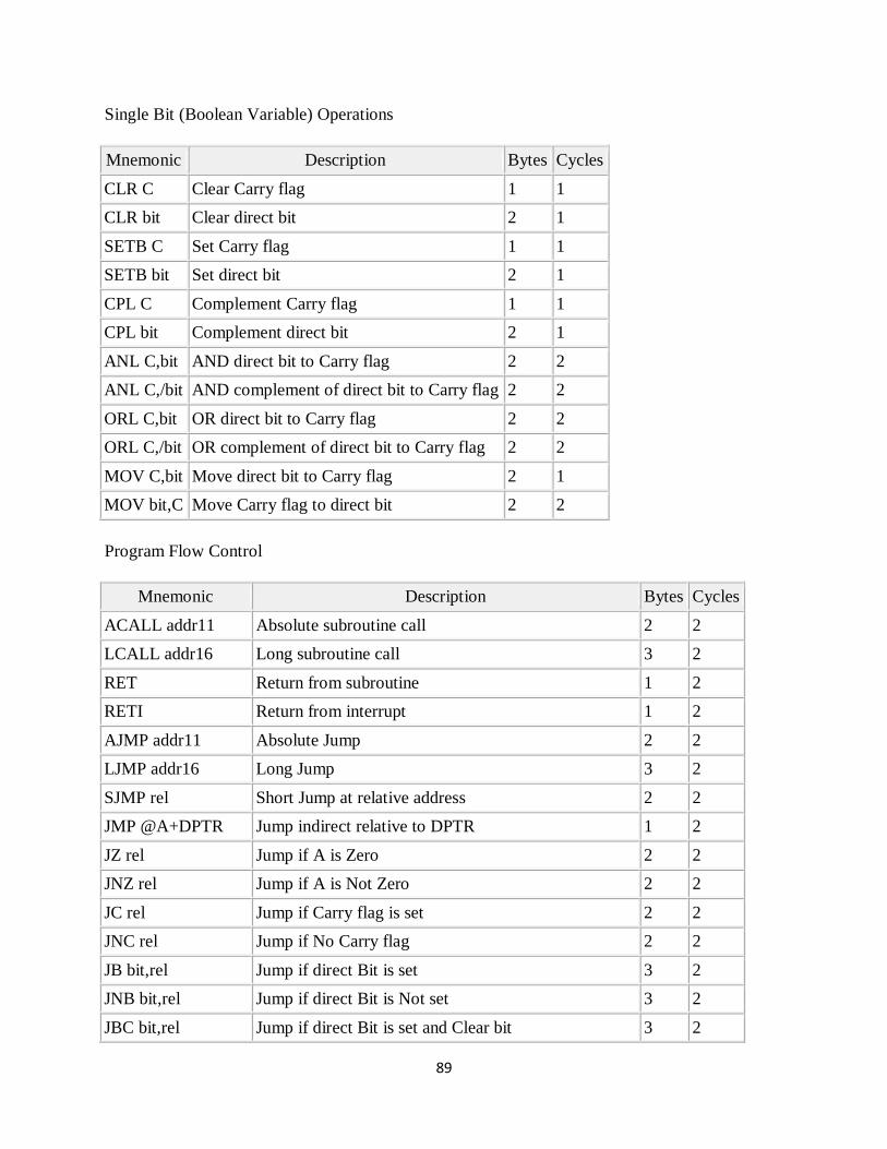
89
Single Bit (Boolean Variable) Operations
Mnemonic Description Bytes Cycles
CLR C Clear Carry flag 1 1 CLR bit Clear direct bit 2 1
SETB C Set Carry flag 1 1 SETB bit Set direct bit 2 1
CPL C Complement Carry flag 1 1 CPL bit Complement direct bit 2 1
ANL C,bit AND direct bit to Carry flag 2 2 ANL C,/bit AND complement of direct bit to Carry flag 2 2
ORL C,bit OR direct bit to Carry flag 2 2 ORL C,/bit OR complement of direct bit to Carry flag 2 2
MOV C,bit Move direct bit to Carry flag 2 1 MOV bit,C Move Carry flag to direct bit 2 2
Program Flow Control
Mnemonic Description Bytes Cycles
ACALL addr11 Absolute subroutine call 2 2 LCALL addr16 Long subroutine call 3 2
RET Return from subroutine 1 2 RETI Return from interrupt 1 2
AJMP addr11 Absolute Jump 2 2 LJMP addr16 Long Jump 3 2
SJMP rel Short Jump at relative address 2 2 JMP @A+DPTR Jump indirect relative to DPTR 1 2
JZ rel Jump if A is Zero 2 2 JNZ rel Jump if A is Not Zero 2 2
JC rel Jump if Carry flag is set 2 2 JNC rel Jump if No Carry flag 2 2
JB bit,rel Jump if direct Bit is set 3 2 JNB bit,rel Jump if direct Bit is Not set 3 2
JBC bit,rel Jump if direct Bit is set and Clear bit 3 2
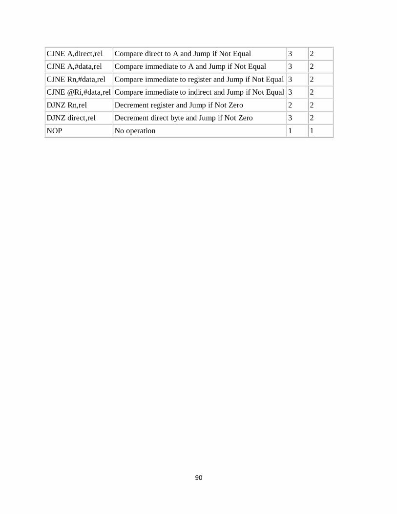
90
CJNE A,direct,rel Compare direct to A and Jump if Not Equal 3 2 CJNE A,#data,rel Compare immediate to A and Jump if Not Equal 3 2
CJNE Rn,#data,rel Compare immediate to register and Jump if Not Equal 3 2 CJNE @Ri,#data,rel Compare immediate to indirect and Jump if Not Equal 3 2
DJNZ Rn,rel Decrement register and Jump if Not Zero 2 2 DJNZ direct,rel Decrement direct byte and Jump if Not Zero 3 2
NOP No operation 1 1

91
Appendix C: System Firmware
ORG 0000H
SENSOR1_OUT BIT P2.6
SENSOR2_OUT BIT P2.5
SENSOR3_OUT BIT P2.4
IGNITIONA BIT P3.0
IGNITIONB BIT P3.1
IGNITION_CONTROL BIT P2.1
BUZZER BIT P2.2
SENSOR1A BIT P0.0
SENSOR1B BIT P0.1
SENSOR1C BIT P0.2
SENSOR2A BIT P0.3
SENSOR2B BIT P0.4
SENSOR2C BIT P0.5
SENSOR3A BIT P0.6
SENSOR3B BIT P0.7
SENSOR3C BIT P2.0
LCD EQU P1
EN BIT P3.7
RW BIT P3.6
RS BIT P3.5
MOV R4,#00H
AJMP MAIN

92
INTCODE:DB 038H,00EH,001H,006H,081H,0
WRTOVER: DB 081H,0
LINE2: DB 0C1H,0
LCD_WRT: CLR A
MOVC A,@A+DPTR
MOV LCD,A
SETB RS
CLR RW
SETB EN
NOP
CLR EN
ACALL DELAY
INC DPTR
JZ CMD
SJMP LCD_WRT
CMD:RET
LCD_CMD: CLR A
MOVC A,@A+DPTR
MOV LCD,A
CLR RS
CLR RW
SETB EN
NOP

93
CLR EN
ACALL DELAY
INC DPTR
JZ CMD1
SJMP LCD_CMD
CMD1:RET
MAIN: MOV P0,#0FFH
MOV P1,#0FFH
MOV P2,#00H
MOV P3,#00H
SETB P3.0
SETB P3.1
clr ignitiona
clr ignitionb
clr sensor3_out
CLR IGNITION_CONTROL
SETB P2.0
CLR SENSOR1_OUT
CLR SENSOR2_OUT
CLR SENSOR3_OUT
START: MOV DPTR,#INTCODE
ACALL LCD_CMD
MOV DPTR,#INTCODE

94
ACALL LCD_CMD
MOV DPTR,#TABLE1
ACALL LCD_WRT
ACALL WAST_TIME2
MOV DPTR,#WRTOVER
ACALL LCD_CMD
MOV DPTR,#CHECKING_OUT
ACALL LCD_WRT
ACALL WAST_TIME
BEGIN1:CLR SENSOR1_OUT
clr ignitiona
clr ignitionb
clr sensor3_out
SENSOR1:
JB SENSOR1A,sensor2
se1: JB SENSOR1B, sensor2
se2: JB SENSOR1C,SENSOR2
CLR SENSOR2_OUT
CLR SENSOR3_OUT
SETB SENSOR1_OUT
CLR IGNITIONA
CLR IGNITIONB
MOV DPTR,#WRTOVER
ACALL LCD_CMD

95
MOV DPTR,#STRING1
ACALL LCD_WRT
MOV DPTR,#LINE2
ACALL LCD_CMD
MOV DPTR,#STRING1B
ACALL LCD_WRT
BLOOP:MOV R3,P0
JB SENSOR1A,SENSOR2
JB SENSOR1B, SENSOR2
JB SENSOR1C,SENSOR2
CJNE R3,#00011111B,B1
B1: CJNE R3,#00000011B,B2
B2: CJNE R3,#00H,BEGIN1
B3: SJMP BLOOP
SEC30:ACALL WAST_TIME2
ACALL WAST_TIME2
ACALL WAST_TIME2
AJMP SENSOR1
BEGIN2: CLR SENSOR2_OUT
SENSOR2:JNB SENSOR1A,SEC30
JNB SENSOR1B,SEC30
JNB SENSOR1C,SEC30

96
s20: JB SENSOR2A,route
s21: JB SENSOR2B,route
s22: JB SENSOR2C,route
CLR IGNITIONA
CLR IGNITIONB
CLR SENSOR3_OUT
CLR SENSOR1_OUT
SETB SENSOR2_OUT
MOV DPTR,#WRTOVER
ACALL LCD_CMD
MOV DPTR,#STRING2
ACALL LCD_WRT
MOV R3,#0FFH
BLOOP2:JNB SENSOR1A,SEC30
JNB SENSOR1B,SEC30
JNB SENSOR1C,SEC30
MOV R3,P0
CJNE R3,#11100011B,B12
B12: CJNE R3,#11100000B,BEGIN2
SJMP BLOOP2
amen: ajmp resd
ROUTE:
DIS: MOV DPTR,#WRTOVER

97
ACALL LCD_CMD
MOV DPTR,#STRING5
ACALL LCD_WRT
MOV DPTR,#LINE2
ACALL LCD_CMD
MOV DPTR,#STRING5B
ACALL LCD_WRT
jb ignition_control,amen
ok:
setb IGNITIONA
setb IGNITIONB
acall wast_time
acall wast_time
CLR IGNITIONA
INC R4
JNB SENSOR3A,SENSOR3
JNB SENSOR3B,SENSOR3
JNB SENSOR3C,SENSOR3
CO1: ACALL WAST_TIME2
CJNE R4,#3h,ok
MOV R4,#00
AJMP resd
sec30x: ajmp sec30

98
SENSOR3: JB IGNITION_CONTROL,MON1
JNB SENSOR2A,SEC31
JNB SENSOR2B,SEC31
JNB SENSOR2C,SEC31
JNB SENSOR1A,SEC30x
JNB SENSOR1B,SEC30x
JNB SENSOR1C,SEC30x
JB SENSOR3A,COMPLETE
JB SENSOR3B, COMPLETE
JB SENSOR3C,COMPLETE
CLR SENSOR2_OUT
CLR SENSOR1_OUT
SETB SENSOR3_OUT
MOV DPTR,#intcode
ACALL LCD_CMD
MOV DPTR,#STRING3
ACALL LCD_WRT
MOV DPTR,#LINE2
ACALL LCD_CMD
MOV DPTR,#STRING1B
ACALL LCD_WRT
ACALL WAST_TIME
CLR IGNITIONA
MON1:JB IGNITION_CONTROL,SWG

99
JNB SENSOR2A,SEC31
JNB SENSOR2B,SEC31
JNB SENSOR2C,SEC31
JNB SENSOR1A,SEC30x
JNB SENSOR1B,SEC30x
JNB SENSOR1C,SEC30x
JB SENSOR3A,COMPLETE
JB SENSOR3B, COMPLETE
JB SENSOR3C,COMPLETE
SJMP MON1
SWG:
CLR SENSOR3_OUT
CLR IGNITIONA
AJMP SENSOR1
COMPLETE:CLR SENSOR3_OUT
JNB SENSOR1_OUT,RESD
JNB SENSOR2_OUT,RESD
JNB SENSOR3_OUT,RESD
RETURN: AJMP SENSOR1
SEC31:ACALL WAST_TIME2
ACALL WAST_TIME2
ACALL WAST_TIME2
AJMP SENSOR2
RESD: MOV DPTR,#intcode

100
ACALL LCD_CMD
MOV DPTR,#STRING4
ACALL LCD_WRT
SJMP ALARM
ALARM:MOV R3,P0
clr sensor3_out
clr ignitiona
clr ignitionb
return1:
ACALL BUZZER_OUT
mov r3,p0
cjne r3,#0ffh,next3
ajmp alarm
next3: AJMP sensor1
; SUB ROUTINGS COUNTS
WAST_TIME: MOV R7,#00
HERE: INC R7
ACALL DELAY
CJNE R7,#60,HERE
MOV R7,#00
RET

101
WAST_TIME2: MOV R7,#00
HERE2: INC R7
ACALL DELAY
CJNE R7,#200,HERE2
MOV R7,#00
RET
DELAY: MOV R0,#255
MOV R1,#10
MOV R2,#1
LOOP: DJNZ R0,LOOP
DJNZ R1,LOOP
DJNZ R2,LOOP
RET
TABLE1: DB 'WELCOME',0
CHECKING_OUT: DB 'SCANING BUTTON',0
BUZZER_OUT: jb ignition_control,rest
SETB BUZZER
ACALL WAST_TIME2
CLR BUZZER
ACALL WAST_TIME2
rest: RET

102
STRING1: DB 'PUBLIC POWER ',0
STRING1B:DB 'SUPPLY',0
STRING2: DB 'SOLAR POWER ',0
STRING3: DB ' GENERATOR ......',0
STRING4: DB 'LOSS OF POWER',0
STRING5: DB 'BACKUP GEN ',0
STRING5B: DB ' LOADING ',0
END
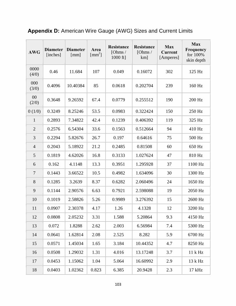
103
Appendix D: American Wire Gauge (AWG) Sizes and Current Limits
AWG Diameter [inches]
Diameter [mm]
Area [mm2]
Resistance [Ohms / 1000 ft]
Resistance [Ohms /
km]
Max Current
[Amperes]
Max Frequency for 100% skin depth
0000 (4/0) 0.46 11.684 107 0.049 0.16072 302 125 Hz
000 (3/0) 0.4096 10.40384 85 0.0618 0.202704 239 160 Hz
00 (2/0) 0.3648 9.26592 67.4 0.0779 0.255512 190 200 Hz
0 (1/0) 0.3249 8.25246 53.5 0.0983 0.322424 150 250 Hz
1 0.2893 7.34822 42.4 0.1239 0.406392 119 325 Hz
2 0.2576 6.54304 33.6 0.1563 0.512664 94 410 Hz
3 0.2294 5.82676 26.7 0.197 0.64616 75 500 Hz
4 0.2043 5.18922 21.2 0.2485 0.81508 60 650 Hz
5 0.1819 4.62026 16.8 0.3133 1.027624 47 810 Hz
6 0.162 4.1148 13.3 0.3951 1.295928 37 1100 Hz
7 0.1443 3.66522 10.5 0.4982 1.634096 30 1300 Hz
8 0.1285 3.2639 8.37 0.6282 2.060496 24 1650 Hz
9 0.1144 2.90576 6.63 0.7921 2.598088 19 2050 Hz
10 0.1019 2.58826 5.26 0.9989 3.276392 15 2600 Hz
11 0.0907 2.30378 4.17 1.26 4.1328 12 3200 Hz
12 0.0808 2.05232 3.31 1.588 5.20864 9.3 4150 Hz
13 0.072 1.8288 2.62 2.003 6.56984 7.4 5300 Hz
14 0.0641 1.62814 2.08 2.525 8.282 5.9 6700 Hz
15 0.0571 1.45034 1.65 3.184 10.44352 4.7 8250 Hz
16 0.0508 1.29032 1.31 4.016 13.17248 3.7 11 k Hz
17 0.0453 1.15062 1.04 5.064 16.60992 2.9 13 k Hz
18 0.0403 1.02362 0.823 6.385 20.9428 2.3 17 kHz
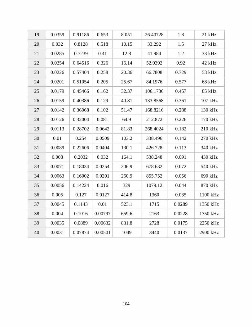
104
19 0.0359 0.91186 0.653 8.051 26.40728 1.8 21 kHz
20 0.032 0.8128 0.518 10.15 33.292 1.5 27 kHz
21 0.0285 0.7239 0.41 12.8 41.984 1.2 33 kHz
22 0.0254 0.64516 0.326 16.14 52.9392 0.92 42 kHz
23 0.0226 0.57404 0.258 20.36 66.7808 0.729 53 kHz
24 0.0201 0.51054 0.205 25.67 84.1976 0.577 68 kHz
25 0.0179 0.45466 0.162 32.37 106.1736 0.457 85 kHz
26 0.0159 0.40386 0.129 40.81 133.8568 0.361 107 kHz
27 0.0142 0.36068 0.102 51.47 168.8216 0.288 130 kHz
28 0.0126 0.32004 0.081 64.9 212.872 0.226 170 kHz
29 0.0113 0.28702 0.0642 81.83 268.4024 0.182 210 kHz
30 0.01 0.254 0.0509 103.2 338.496 0.142 270 kHz
31 0.0089 0.22606 0.0404 130.1 426.728 0.113 340 kHz
32 0.008 0.2032 0.032 164.1 538.248 0.091 430 kHz
33 0.0071 0.18034 0.0254 206.9 678.632 0.072 540 kHz
34 0.0063 0.16002 0.0201 260.9 855.752 0.056 690 kHz
35 0.0056 0.14224 0.016 329 1079.12 0.044 870 kHz
36 0.005 0.127 0.0127 414.8 1360 0.035 1100 kHz
37 0.0045 0.1143 0.01 523.1 1715 0.0289 1350 kHz
38 0.004 0.1016 0.00797 659.6 2163 0.0228 1750 kHz
39 0.0035 0.0889 0.00632 831.8 2728 0.0175 2250 kHz
40 0.0031 0.07874 0.00501 1049 3440 0.0137 2900 kHz
Related Documents