Article Materials Science Efficient perovskite solar cells based on novel three-dimensional TiO 2 network architectures Hao Lu • Kaimo Deng • Nina Yan • Yulong Ma • Bangkai Gu • Yong Wang • Liang Li Received: 19 January 2016 / Revised: 24 February 2016 / Accepted: 8 March 2016 / Published online: 1 April 2016 Ó Science China Press and Springer-Verlag Berlin Heidelberg 2016 Abstract Mesoscopic lead halide perovskite solar cells typically use TiO 2 nanoparticle films as the scaffolds for electron-transport pathway and perovskite deposition. Here, we demonstrate that swelling-induced mesoporous block copolymers can be templates for producing three- dimensional TiO 2 networks by combining the atomic layer deposition technique. Thickness adjustable TiO 2 network is an excellent alternative scaffold material for efficient per- ovskite solar cells. Our best performing cells using such a 270 nm thick template have achieved a high efficiency of 12.5 % with pristine poly-3-hexylthiophene as a hole transport material. The high performance is attributed to the direct transport pathway and high absorption of scaf- folds, small leakage current and largely reduced recombi- nation rate at interfaces. The results show that TiO 2 network architecture is a promising scaffold for meso- scopic perovskite solar cells. Keywords Perovskite Á Solar cell Á TiO 2 Á Template Á Atomic layer deposition 1 Introduction Solar cells directly converting solar energy into electricity have been recognized as an alternative energy source for our planet in the future considering the global shortage of fossil fuels. In recent decades, silicon solar cells have a rather high market share worldwide, but their further development is facing a great challenge to balance the power conversion efficiency (PCE) and the cost. It is known that crystalline silicon solar cells have a relatively high PCE and a high cost. However, thin film silicon solar cells are much cheaper due to the use of fewer raw materials. In spite of this, relatively low PCEs limit their large scale production. Developing solar cells with low cost and high PCEs is in great demand nowadays. Among the various types of solar cells, organic- inorganic hybrid perovskite solar cells are most likely to stand out [1]. On the one hand, perovskite solar cells can be fabricated by solution processing or chemical vapor depo- sition, both of which are beneficial for cost reduction and mass production [2, 3]. On the other hand, solar cells of this type are undergoing a rapid development since they have taken only about five years to raise the PCE from 4 % to 20 % [4], a value comparable to that of crystalline silicon solar cells. The most fascinating gemini of organic-inorganic hybrid perovskites for solar cells are CH 3 NH 3 PbI 3 and CH 3 NH 3 PbI 3-x Cl x , which have a suitable bandgap about 1.55 eV for visible light absorption. To realize easy fabri- cation and excellent performance of organic-inorganic hybrid perovskite solar cells, much efforts have been devoted to designing a more suitable architecture and modifying the interface property of different contact layers [5, 6]. Hao Lu and Kaimo Deng contributed equally to this work. Electronic supplementary material The online version of this article (doi:10.1007/s11434-016-1050-x) contains supplementary material, which is available to authorized users. H. Lu Á K. Deng Á Y. Ma Á B. Gu Á L. Li (&) College of Physics, Optoelectronics and Energy, Center for Energy Conversion Materials and Physics (CECMP), Jiangsu Key Laboratory of Thin Films, Soochow University, Suzhou 215006, China e-mail: [email protected] N. Yan Á Y. Wang (&) State Key Laboratory of Materials-Oriented Chemical Engineering, College of Chemical Engineering, Nanjing Tech University, Nanjing 210009, China e-mail: [email protected] 123 Sci. Bull. (2016) 61(10):778–786 www.scibull.com DOI 10.1007/s11434-016-1050-x www.springer.com/scp

Welcome message from author
This document is posted to help you gain knowledge. Please leave a comment to let me know what you think about it! Share it to your friends and learn new things together.
Transcript

Artic le Materials Science
Efficient perovskite solar cells based on novel three-dimensionalTiO2 network architectures
Hao Lu • Kaimo Deng • Nina Yan • Yulong Ma •
Bangkai Gu • Yong Wang • Liang Li
Received: 19 January 2016 / Revised: 24 February 2016 / Accepted: 8 March 2016 / Published online: 1 April 2016
� Science China Press and Springer-Verlag Berlin Heidelberg 2016
Abstract Mesoscopic lead halide perovskite solar cells
typically use TiO2 nanoparticle films as the scaffolds for
electron-transport pathway and perovskite deposition.
Here, we demonstrate that swelling-induced mesoporous
block copolymers can be templates for producing three-
dimensional TiO2 networks by combining the atomic layer
deposition technique. Thickness adjustable TiO2 network is
an excellent alternative scaffold material for efficient per-
ovskite solar cells. Our best performing cells using such a
270 nm thick template have achieved a high efficiency of
12.5 % with pristine poly-3-hexylthiophene as a hole
transport material. The high performance is attributed to
the direct transport pathway and high absorption of scaf-
folds, small leakage current and largely reduced recombi-
nation rate at interfaces. The results show that TiO2
network architecture is a promising scaffold for meso-
scopic perovskite solar cells.
Keywords Perovskite � Solar cell � TiO2 �Template � Atomic layer deposition
1 Introduction
Solar cells directly converting solar energy into electricity
have been recognized as an alternative energy source for our
planet in the future considering the global shortage of fossil
fuels. In recent decades, silicon solar cells have a rather high
market share worldwide, but their further development is
facing a great challenge to balance the power conversion
efficiency (PCE) and the cost. It is known that crystalline
silicon solar cells have a relatively high PCE and a high cost.
However, thin film silicon solar cells are much cheaper due
to the use of fewer raw materials. In spite of this, relatively
low PCEs limit their large scale production. Developing
solar cells with low cost and high PCEs is in great demand
nowadays. Among the various types of solar cells, organic-
inorganic hybrid perovskite solar cells are most likely to
stand out [1]. On the one hand, perovskite solar cells can be
fabricated by solution processing or chemical vapor depo-
sition, both of which are beneficial for cost reduction and
mass production [2, 3]. On the other hand, solar cells of this
type are undergoing a rapid development since they have
taken only about five years to raise the PCE from 4 % to
20 % [4], a value comparable to that of crystalline silicon
solar cells. Themost fascinating gemini of organic-inorganic
hybrid perovskites for solar cells are CH3NH3PbI3 and
CH3NH3PbI3-xClx, which have a suitable bandgap about
1.55 eV for visible light absorption. To realize easy fabri-
cation and excellent performance of organic-inorganic
hybrid perovskite solar cells,much efforts have been devoted
to designing a more suitable architecture and modifying the
interface property of different contact layers [5, 6].
Hao Lu and Kaimo Deng contributed equally to this work.
Electronic supplementary material The online version of thisarticle (doi:10.1007/s11434-016-1050-x) contains supplementarymaterial, which is available to authorized users.
H. Lu � K. Deng � Y. Ma � B. Gu � L. Li (&)
College of Physics, Optoelectronics and Energy, Center for
Energy Conversion Materials and Physics (CECMP), Jiangsu
Key Laboratory of Thin Films, Soochow University,
Suzhou 215006, China
e-mail: [email protected]
N. Yan � Y. Wang (&)
State Key Laboratory of Materials-Oriented Chemical
Engineering, College of Chemical Engineering, Nanjing Tech
University, Nanjing 210009, China
e-mail: [email protected]
123
Sci. Bull. (2016) 61(10):778–786 www.scibull.com
DOI 10.1007/s11434-016-1050-x www.springer.com/scp

Typical device architectures of perovskite solar cells
include six parts: conductive glass (fluorine-doped tin oxides
(FTO) or indium tin oxides (ITO)) substrate, hole-blocking
layer, scaffold materials, hole-transport materials (HTM),
organometal-halide perovskite layer andmetal cathode (Auor
Ag). TiO2 is the most frequently used charge-injecting and
hole-blocking oxide due to its large energy band gap,matched
energy level and high carrier mobility. In a typical process,
two fabrication steps are required before perovskite deposi-
tion [7, 8]. First, a compact TiO2 layer is initially formed on
the conductive glass substrate to function as hole-blocking
layer. Then, a TiO2 nanoparticle layer serves as both the
electron-transport pathway and mesoporous frame structure
for perovskite deposition. Snaith and co-workers [9] reported
that Al2O3 nanoparticle layer could also function well as the
mesoporous frame structure although it is an insulator. The
advantage of mesoscopic type solar cells is that the meso-
porous nanoparticle layer can favor the formation of a thick
perovskite layer, resulting in increased light capture and a
high current density. In recent years, the planar type solar cells
which do not use the nanoparticles layer have also been
studied, for its simple fabrication method [3, 10]. Thus it is
quite desirable to achieve a high efficiency of perovskite solar
cells with a simple architecture by combining themerits of the
planar and mesoscopic type solar cells.
The thickness of TiO2 mesoscopic scaffolds should be
lower than the optimum thickness of the perovskite layer,
which is typically about 300–500 nm in consideration of the
diffusion length of electrons and holes in perovskite solar
cells. This requirement limits the choice of template scaf-
folds. Owing to the facile synthesis and controlled height,
one-dimensional nanorod/nanowire arrays have been widely
investigated as potential alternatives to nanoparticles. Bi
et al. [11] reported ZnO nanorod arrays based perovskite
solar cell with efficiency about 5 %, which was much lower
than traditional planar or mesoporous cells. Mahmood et al.
[12] presented ZnO nanostructures based perovskite solar
cell with the highest efficiency about 10 %, in which a
number of growth processes should be controlled. Kim et al.
[13] showed perovskite solar cell based on TiO2 nanorod
arrays with an efficiency of 9.4 %. Recently, Fakharuddin
et al. [14] reported TiO2 nanorods based perovskite solar
cells with efficiency about 10.5 %, which used an interface
engineering during growth processes and an optimized laser
pulse for patterning. Therefore, it is challenging to explore
more efficient nanoporous materials as mesoscopic scaffolds
with excellent hole-blocking and electron-transporting
property. Selective swelling-induced pore generation of
amphiphilic block copolymers (BCPs) has emerged as a
facile and efficient strategy for the preparation mesoporous
networks with three-dimensionally interconnected porosi-
ties. The thicknesses of the porous networks can be con-
tinuously tuned from nanoscale to bulk simply by
controlling the coating techniques and coating parameters
[15, 16]. Because of the interconnected mesoscopic
porosities and adjustable thicknesses, thus-obtained BCPs
porous networks are expected to be used as interesting
sacrificial templates for the fabrication of perovskite solar
cells with direct charge transport pathways. In order to copy
the specific morphology of the BCP templates, it is impor-
tant to choose an appropriate method for the deposition of
TiO2 on the BCPs templates. Atomic layer deposition
(ALD) is a powerful tool for depositing thin film with great
accuracy in thickness and uniformity at a controllable rate
below 1 nm per cycle. The self-limiting and surface satu-
rated process of ALD endows it the perfect ability to pro-
duce conformal ultrathin films, even on materials with high
aspect ratios [17–19]. ALD technique is generally more
expensive than commonly used sol-gel deposition method
and ALD instrumentation is not available in some settings.
Herein, we employ ALD technique to coat TiO2 films
with different thicknesses on swelling-induced porous
BCPs templates. After a calcining process, BCPs are
removed and mesoporous TiO2 networks are formed with
precisely modulated thicknesses. For the first time, this
novel TiO2 network is used as the mesoporous scaffold for
loading perovskite films. The thicknesses of frame can be
adjusted precisely for effective infiltration of perovskite
precursors. Usually a compact hole-blocking layer is nec-
essary before depositing a mesoporous frame, however,
present solar cells do not need this extra step. The
CH3NH3PbI3-xClx and pristine poly-3-hexylthiophene
(P3HT) are served as the light absorbing layer and HTM,
respectively. P3HT is cheap and easy to use and has been
considered as a suitable HTM for perovskite solar cells
than spiro-MeOTAD, which needs oxidation or doping
treatment in ambient atmosphere. The cell (glass/FTO/
ALD-TiO2 nanostructures/CH3NH3PbI3-xClx/P3HT/Ag)
shows a PCE as high as 12.5 % compared with 9.83 % of
planar TiO2 cells. It is worthy to note that the achieved
efficiency is comparable or even higher than values
reported previously in perovskite solar cells with pristine
P3HT as HTM (Table S1 online). The underlying mecha-
nism for excellent performance has been studied by
investigating the cell parameters including the thickness of
ALD TiO2 layer, morphology of perovskite, transmittance,
leakage current and charge transfer and recombination
processes.
2 Materials and methods
2.1 Preparation of mesoporous templates
The FTO glasses were etched by Zn powder and dilute
hydrochloric acid (HCl, 36.5 %–38.0 %, Alfa) and the
Sci. Bull. (2016) 61(10):778–786 779
123
etched FTO glasses were washed with acetone, ethyl alcohol
and deionized water by turns in an ultrasonic bath for
30 min. The precursor solution was prepared in a fume hood
at room temperature. Firstly, the tetrahydrofuran solution of
3 wt% polystyrene-b-poly(2-vinyl pyridine) (PS-b-P2VP,
Mn,PS = 50,000 g/mol, Mn,P2VP = 16,500 g/mol, Polymer
Source) was spin-coated onto etched FTO substrates at
different speeds to obtain films with various thicknesses
from 180 to 270 and 370 nm. Then swelling-treated in
ethanol at 60 �C for 15 h, ethanol could dissolve with the
polymer during this time. Finally, the substrates were taken
outside the solution followed by air drying, yielding meso-
porous BCP template membranes. Then the obtained tem-
plates were treated in an ALD system (Ensure NanoTech) at
80 �C. Tetra(dimethylamino)titanium (TDMAT, Jiangsu
Nata Opto-electronic Materials Co.) and H2O were used as
precursors and high-purity Ar was used as the TDMAT
carrier and the purging gas. The thickness of the deposited
TiO2 layer was precisely controlled by adjusting the cycle
numbers of ALD. The growth rate of the TiO2 layer during
the ALD process was 0.5 A per cycle. After the deposition,
the ALD coated films were calcined in air at 500 �C for 2 h.
2.2 Solar cell fabrication
The solar cells were fabricated on the as-prepared template
substrates. The perovskite precursor solution was synthe-
sized by dissolving CH3NH3I and PbCl2 (3:1 molar ratio,
45 wt%) in N,N-dimethylformamide (DMF) at 60 �C for
12 h, and then the above precursor solution was filtered
through a 0.45 lm filter. The perovskite layer was prepared
by spin-coating the precursor solutions at 3,000 r/min for
30 s and annealed at 100 �C for 2 h. P3HT layer was
deposited on the top of the perovskite layer by spin-coating
(30 mg P3HT dissolved in 1 mL chlorobenzene solution)
at 2,000 r/min for 40 s. All processes were performed
under controlled nitrogen gas in a glove box. Finally, a
100 nm-thick Ag electrode was deposited by thermal
evaporation with a shadow mask (0.12 cm2 active area).
2.3 Characterization
The morphology of the samples was characterized using
field-emission scanning electron microscope (FE-SEM,
SU8010, Hitachi). The phase of products was checked by
the X-ray diffractometer (XRD, D/MAX-III-B-40KV, Cu
Ka radiation, k = 0.15418 nm). The photocurrent–voltage
(J–V), leakage current curve and incident photon-to-current
conversion efficiency (IPCE) were measured using a
Newport solar simulator under AM1.5 irradiation
(100 mW/cm2). The absorbance and transmission spectra
were detected by a UV–Vis spectrophotometer (Shimadzu
UV-3600). The electrochemical impedance spectroscopy
(EIS) was measured with an electrochemical workstation
(Autolab PGSTAT 302 N) under light at 0 V with the
alternative signal amplitude 5 mV and frequency range
from 4.0 9 105 to 1 Hz.
3 Results and discussion
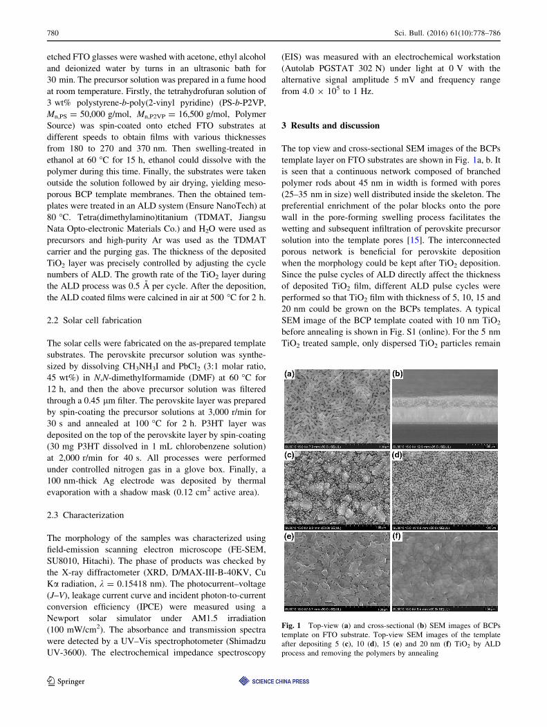
The top view and cross-sectional SEM images of the BCPs
template layer on FTO substrates are shown in Fig. 1a, b. It
is seen that a continuous network composed of branched
polymer rods about 45 nm in width is formed with pores
(25–35 nm in size) well distributed inside the skeleton. The
preferential enrichment of the polar blocks onto the pore
wall in the pore-forming swelling process facilitates the
wetting and subsequent infiltration of perovskite precursor
solution into the template pores [15]. The interconnected
porous network is beneficial for perovskite deposition
when the morphology could be kept after TiO2 deposition.
Since the pulse cycles of ALD directly affect the thickness
of deposited TiO2 film, different ALD pulse cycles were
performed so that TiO2 film with thickness of 5, 10, 15 and
20 nm could be grown on the BCPs templates. A typical
SEM image of the BCP template coated with 10 nm TiO2
before annealing is shown in Fig. S1 (online). For the 5 nm
TiO2 treated sample, only dispersed TiO2 particles remain
Fig. 1 Top-view (a) and cross-sectional (b) SEM images of BCPs
template on FTO substrate. Top-view SEM images of the template
after depositing 5 (c), 10 (d), 15 (e) and 20 nm (f) TiO2 by ALD
process and removing the polymers by annealing
780 Sci. Bull. (2016) 61(10):778–786
123

on the surface of FTO substrates after burning off the BCP
templates (Fig. 1c), which suggests the deposited TiO2
layer is too thin to prevent the collapse of the porous
structures during the calcination process. A thicker (10 nm)
TiO2 layer can help to hold the interconnected TiO2 net-
work with the presence of numerous well distributed pores,
which is verified from Fig. 1d. The corresponding cross-
sectional SEM image is shown in Fig. S2a (online).
Depositing the thick TiO2 layer (15 and 20 nm) on the
templates would seal the porous structure and lead to the
formation of a compact TiO2 film with few or even no
pores (Fig. 1e, f). In this case, the perovskite precursor
solution can hardly penetrate into the TiO2 structures.
Hereafter we chose ALD 10 nm TiO2 deposition as the
optimum parameter for further study. After the template
was removed, another 2 nm TiO2 ALD process was con-
ducted to remedy the pin-holes caused by the escape of
gasified products of degrading polymers. The transmittance
curves of different ALD treated samples were tested and
the 10 nm TiO2 treated film shows a transmittance close to
that of the pure FTO glass as shown in Fig. S2b (online).
As the thickness of templates will significantly influence
the deposition of the perovskite, we prepared FTO sub-
strates supported BCPs templates with the thickness of 180,
270 and 370 nm using different coating speeds. After
10 nm TiO2 ALD process and calcination, we measured
the light transmittance of the obtained TiO2 mesoscopic
structures and the 10 nm TiO2 ALD treated planar film
(Fig. 2a). It is worthy to note that the better light utilization
requires a higher transmittance, so that light has more
chance to be absorbed by the perovskite layer. Although all
the transmittance patterns have a high value in the visible-
near infrared range, as expected that TiO2 mesoscopic
structures have a little lower transmittance compared with
the TiO2 planar film. It can also be found that the trans-
mittance decreases with increased template thickness,
especially in the short wavelength range from 350 to
500 nm. The absorption spectra of corresponding meso-
scopic and planar perovskite (CH3NH3PbI3-xClx) layers
were also measured as shown in Fig. 2b. The perovskite
layer deposited on TiO2 planar film exhibits a relatively
low absorption from 350 to 760 nm. The perovskite layer
supported on TiO2 mesoscopic structure shows an
enhanced light absorption and the intensity increases with
the increased template thickness, suggesting that a thicker
template may favor more perovskite deposition. Figure 2c
shows the top-view SEM image of perovskite layer on a
TiO2 planar film. On the surface of the TiO2 planar film,
nearly no pinholes have been found under a low SEM
magnification, which is similar to our previous report [20].
However, pinholes turn up in the perovskite layers sup-
ported on TiO2 mesoscopic structures. As the thickness of
template increases to 270 nm, densely distributed small
pinholes are replaced by sparsely scattered big ones on the
perovskite surface with basically the same coverage rate
over 90 % (Fig. 2d, e). In fact, the existence of pinholes in
mesoscopic systems does not mean a direct contact
between electron-transport materials (ETM) and HTM, as
there still has thin perovskite coated on the mesoscopic
skeleton underneath large crystalline grains (Fig. S3
online). Consequently, when the density of pinholes is not
very high in the perovskite layer, the recombination rate
can be low. However, a thicker template results in a sharp
decline in the coverage rate to only about 50 % (Fig. 2f).
The thicker mesoscopic template can accommodate more
precursor solution in pores of networks, so that the residual
solution on the surface of template is not enough to pro-
duce a compact perovskite layer. In this situation, more
light could transmit through the perovskite layer without
being absorbed. Besides, the recombination will become
more serious at the interface even if the coverage of per-
ovskite on the mesoscopic template can eliminate the direct
contact of TiO2 and P3HT. So an expected efficiency might
be achieved utilizing the template with a thickness of 180
or 270 nm, which shows a high transmittance, good
absorption ability and high perovskite coverage rate.
Figure 3a, b show the cross-sectional SEM images of
the CH3NH3PbI3-xClx layer covered on planar TiO2 film
and 270 nm-thick TiO2 mesoscopic structures, respec-
tively. The cross sectional SEM images of other samples
could be found in Fig. S4 (online). The compact
CH3NH3PbI3-xClx layers on the top of TiO2 mesoscopic
structures and on TiO2 planar film have the almost identical
thickness 500–600 nm. In addition, the internal space of
the TiO2 mesoscopic structures is completely filled by
CH3NH3PbI3-xClx. This special interface design makes
charge separation more easily from bulk perovskite to TiO2
network and the TiO2 mesoscopic structures provide a
direct pathway for charge transport to the conductive glass,
reducing transfer resistance and recombination rate. The
structural properties of the perovskite layers were checked
by XRD. As shown in Fig. 3c, all the XRD patterns exhibit
three main diffraction peaks at 14.2�, 28.5� and 42.8�,which are assigned to the (110), (220) and (330) crystalline
plane of CH3NH3PbI3-xClx, respectively. It indicates that
TiO2 mesoscopic structures will not induce extra preferred
orientation during perovskite crystallization and a well-
crystallized perovskite film can be obtained.
After spin-coating P3HT as a hole-transport material
and evaporating a thin silver film as the back contact
electrode, perovskite solar cells based on TiO2 planar films
and TiO2 mesoscopic structures were characterized by
photovoltaic measurements. Figure 4a shows the J–
V curves of the corresponding perovskite solar cells under a
solar simulator with a power density of 100 mW/cm2. The
photovoltaic parameters, including open-circuit voltage
Sci. Bull. (2016) 61(10):778–786 781
123

(Voc), short-current density (Jsc), fill factor (FF) and PCE,
are listed in Table 1. The device based on a TiO2 planar
film delivers Voc of 0.9 V, Jsc of 18 mA/cm2, FF of 60.7 %
and PEC of 9.83 %. Perovskite solar cell with a 180 nm-
thick TiO2 mesoscopic structure has the higher PCE, which
is mainly attributed to the enhanced Jsc. A device derived
from thicker template of 270 nm displays the best perfor-
mance with Voc of 0.92 V, Jsc of 21.5 mA/cm2, FF of
60.3 % and PEC of 12.5 %. However, further increasing
template thickness results in relatively low Jsc, Voc and
poor PCE. It is believed that the low perovskite coverage
rate has a detrimental effect on the photovoltaic
performance by reducing light capture ability and intro-
ducing more recombination centers. The obtained Jsc val-
ues were also confirmed by incident photon-to-current
conversion efficiency (IPCE) spectra. Figure 4b shows the
IPCE curves and the corresponding integrated current-
density of perovskite solar cells. The integrated current
density is in good agreement with the result in J–V curves,
demonstrating the J–V measurement in our experiments is
reliable. It is clear that 270 nm-template based device
achieves the best external quantum efficiency (EQE) from
350 to 750 nm. All the curves have a sharp decrease around
760 nm which is consistent with the bandgap (*1.55 eV)
Fig. 2 (Color online) a Light transmittance spectra of the TiO2 mesoscopic films with different thicknesses and the 10 nm TiO2 ALD treated
planar film. b The absorption spectra of corresponding mesoscopic and planar perovskite (CH3NH3PbI3-xClx) layers. Top-view SEM image of
perovskite layer on TiO2 planar film (c), 180 (d), 270 (e) and 370 nm (f) thick TiO2 mesoscopic structures
782 Sci. Bull. (2016) 61(10):778–786
123

of perovskite. Compared with the device based on planar
films, the improved Jsc and EQE of the champion device
are related to the more perovskite loading into the template
and thus more intense light absorption, as manifested by
the aforementioned absorption spectra. The previous
reports [21–23] showed that the scanning rate during J–
V curve measurement might influence efficiency. Figure 4c
shows the J–V curves of the best performance device under
various scanning rates from 0.6 to 0.2 V/s and the data are
summarized in Table S2 (online). Our measurement shows
that a decreased scanning rate leads to an obviously
decreased Jsc and increased FF. Compared with the PCE of
12.5 % with a scanning rate of 0.6 V/s, a PCE of 12.0 % is
obtained with a scanning rate of 0.2 V/s, illustrating that
96 % of the initial efficiency can be maintained. The
Fig. 3 (Color online) Cross-sectional SEM images of the
CH3NH3PbI3-xClx layer covered on planar TiO2 film (a) and the
270 nm-thick TiO2 mesoscopic structures (b). c Corresponding XRD
patterns of CH3NH3PbI3-xClx layer
Fig. 4 (Color online) J–V curves (a) and IPCE spectra (b) of
perovskite solar cells based on TiO2 planar films and TiO2
mesoscopic structures with different template thicknesses. c J–
V curves of 270 nm-template based device under various scanning
rates
Sci. Bull. (2016) 61(10):778–786 783
123

present efficiency is higher compared with previously
reported perovskite solar cells with pristine P3HT as HTM,
as shown in Table S1 (online). The solar cells are stable,
which can be reflected from the variation trend of Jsc and
PCE (Fig. S5 online). About 70 % of the initial values are
remained after 130 min of continuous operation.
In order to ensure the credibility of our results, we have
fabricated and tested seven batches of devices containing
35 cells. The average photovoltaic parameters are shown in
Figs. 5 and S6 (online). The Voc, Jsc and PCE of the devices
based on TiO2 planar film and TiO2 mesoscopic structure
with various thicknesses share the same changing tendency
with a low variance, while the change of FF shows a dif-
ferent dependence, which might be blamed on the different
charge transport mode between planar and mesoscopic
types. It is obvious that 270 nm template based devices
achieve the highest value in seven batches. These data
indicate the excellent repeatability and fabrication pro-
cesses of our devices.
In order to explore the internal electrical properties of
different devices, the leakage current and EIS curves were
also measured. The leakage current measurement can pro-
vide the information about the blocking ability of the devi-
ces. The curves in Fig. 6a show that all the devices have a
rather low leakage current. The 10 nmALDTiO2 planar film
based perovskite solar cells have the highest leakage current
among these devices and the other three mesoscopic devices
show a similar lower value. The results provide solid evi-
dence that increasing the thickness of BCPs template does
not introduce too much extra defects in mesoscopic struc-
tures. Especially, for the template based devices, there is no
charge blocking layer introduced on the FTO substrates
before the TiO2 ALD process on the BCPs templates.
EIS is a powerful tool to study the transport and
recombination dynamics of internal carriers [24, 25]. EIS
curves can be fitted with direct values typically represented
by series resistance (Rs), transfer resistance (Rct) and
recombination impedance (Rrec), which are characteristic
parameters for the reaction process at different interfaces.
Herein the EIS measurement was conducted with zero bias
voltage under AM 1.5 G illuminations and a perturbation
voltage of 5 mV was used to record the system response in
a wide frequency range. In Fig. 6b, we can find two
semicircles in the high frequency and one transmission line
in the low frequency for the planar type cells. As we dis-
cussed in our previous work [20], we regarded the two
semicircles in the high frequency region as the Rct between
perovskite/TiO2 and TiO2/FTO interface and considered
the transmission line as Rrec of perovskite layer to the ETM
or the HTM. As for the mesoscopic structure based devi-
ces, the different phenomenon can be found that the two
independent semicircles change to one semicircle in the
high frequency. The change in the high frequency may be
related to the special three-dimensional (3D) templates,
which supply a larger surface area between perovskite and
TiO2 and make carriers separation more easily than planar
one. In the low frequency range, it is found that template
based perovskite solar cells have a lower recombination
resistance. The strongly interconnected TiO2 network in
the mesoscopic structures provides lots of direct transport
pathway. Carriers can transport rapidly from bulk per-
ovskite to FTO glass and will no longer gather in the
interface. Both the fast carrier separation and transport
contribute to the lowered recombination in template based
solar cells. In traditional planar cells, carriers transport
from bulk perovskite to TiO2 then to conduct glass. The
carriers near the interface can be separated fast while
Table 1 The photovoltaic parameters of different perovskite solar
cells
Sample Voc (V) Jsc (mA/cm2) FF (%) PCE (%)
Planar 0.90 18.0 60.7 9.83
180 nm 0.91 20.6 56.3 10.6
270 nm 0.92 21.5 60.3 12.5
370 nm 0.89 16.5 49.2 7.25
Fig. 5 (Color online) The average photovoltaic parameters of
perovskite solar cells with different architectures. a Voc, Jsc. b FF,
PCE
784 Sci. Bull. (2016) 61(10):778–786
123

carriers away from the interface may gather on the surface.
Based on these considerations, a modified equivalent cir-
cuit is illustrated in the inset of Fig. 6c to give a good fit to
template-based solar cells. The model consists of Rs, Rct
and Rrec, and their values of each solar cell are listed in
Table 2. The planar type device shows the lowest Rs value
and Rs of template based perovskite solar cells increases
with the template thickness. Since Rs has an important
effect on FF, a lower Rs may get a higher FF which is
consistent with the J–V results. For the template based
devices, with the increased thickness of template, the value
of Rct becomes higher because the increased TiO2 thickness
means a longer transport pathway. On the other hand, the
increased TiO2 thickness results in more TiO2/perovskite
surface area and at the same time the increased transport
length makes more recombination happen. The results of
the EIS parameters show that 270 nm thick template based
perovskite solar cells have balanced properties in Rrec, Rct
and Rs, which are responsible for the excellent photovoltaic
performance. Moreover, the EIS of 270 nm thickness
template cells with different voltages were also tested and
the curves are shown in Fig. 6d. It is expected that the
increased voltages make a gradually decrease on the radii
of semicircle.
4 Conclusions
In summary, we have combined the mesoporous templates
of block copolymers with ALD technology to obtain a
unique mesoscopic TiO2 network structure with direct
transport pathway and high surface area on FTO glass. A
mesoscopic perovskite cell (FTO/ALD-TiO2 template/
CH3NH3PbI3-xClx/P3HT/Ag) with a high efficiency of
12.5 % has been fabricated. The effect of the TiO2 ALD
coating cycles and the thickness of the template on optical
and electrochemical properties were investigated system-
atically. The optimum performance of the 270 nm thick
template based device is attributed to the direct transport
pathway and high absorption of scaffolds, small leakage
current and largely reduced recombination rate at
Fig. 6 (Color online) Leakage current (a) and EIS curves (b) of perovskite solar cells based on TiO2 planar films and mesoscopic structures
with different template thicknesses. c Magnified curve in the high frequency region for the planar device. The inset is an equivalent circuit for
fitting the EIS. d EIS of 270 nm thickness template cells with different applied voltages during measurement
Table 2 The EIS parameters of different perovskite solar cells
Sample Rs (X) Rct1 (X) Rct2 (X) Rct Rrec (X)
Planar 18.3 355.9 819.8 1175.7 744.3
180 nm 52.2 – – 318.4 711
270 nm 76.3 – – 598.2 317.4
370 nm 88.7 – – 825.3 354
Sci. Bull. (2016) 61(10):778–786 785
123

interfaces. The performance of the TiO2 mesoscopic
structure based devices may be further improved by using
doped P3HT as HTM.
Acknowledgments This work was supported by the National Nat-
ural Science Foundation of China (51422206, 51372159, and
11304217), 1000 Youth Talents Plan, Jiangsu Shuangchuang Plan,
Distinguished Young Scholars Foundation by Jiangsu Science and
Technology Committee (BK20140009) and the Priority Academic
Program Development of Jiangsu Higher Education Institutions
(PAPD).
Conflict of interest The authors declare that they have no conflict
of interest.
References
1. Jung H, Park N (2015) Perovskite solar cells: from materials to
devices. Small 11:10–25
2. Liu C, Wang K, Du P et al (2015) Efficient solution-processed
bulk heterojunction perovskite hybrid solar cells. Adv Energy
Mater 5:1402024
3. Liu M, Johnston MB, Snaith HJ (2013) Efficient planar hetero-
junction perovskite solar cells by vapour deposition. Nature
501:395–398
4. Zhou H, Chen Q, Li G et al (2014) Interface engineering of
highly efficient perovskite solar cells. Science 345:542–546
5. Lee JW, Lee SH, Ko HS et al (2015) Opto-electronic properties
of TiO2 nanohelices with embedded HC(NH2)2PbI3 perovskite
solar cells. J Mater Chem A 3:9179–9186
6. Zhou Z, Pang S, Liu Z et al (2015) Interface engineering for high-
performance perovskite hybrid solar cells. J Mater Chem A
3:19205–19217
7. Im J, Jang I, Pellet N et al (2014) Growth of CH3NH3PbI3cuboids with controlled size for high-efficiency perovskite solar
cells. Nat Nanotechnol 9:927–932
8. Zhu L, Shi J, Lv S et al (2015) Temperature-assisted controlling
morphology and charge transport property for highly efficient
perovskite solar cells. Nano Energy 15:540–548
9. Lee MM, Teuscher J, Miyasaka T et al (2012) Efficient hybrid
solar cells based on meso-superstructured organometal halide
perovskites. Science 338:643–647
10. Ahn N, Son D, Jang I et al (2015) Highly reproducible perovskite
solar cells with average efficiency of 18.3 % and best efficiency
of 19.7 % fabricated via Lewis base adduct of lead(II) iodide.
J Am Chem Soc 137:8696–8699
11. Bi D, Boschloo G, Schwarzmuller S et al (2013) Efficient and
stable CH3NH3PbI3-sensitized ZnO nanorod array solid-state
solar cells. Nanoscale 5:11686–11691
12. Mahmood K, Swain BS, Amassian A (2014) Double-layered ZnO
nanostructures for efficient perovskite solar cells. Nanoscale
6:14674–14678
13. Kim H, Lee J, Yantara N et al (2013) High efficiency solid-state
sensitized solar cell-based on submicrometer rutile TiO2 nanorod
and CH3NH3PbI3 perovskite sensitizer. Nano Lett 13:2412–2417
14. Fakharuddin A, Giacomo F, Palma A et al (2015) Vertical TiO2
nanorods as a medium for stable and high-efficiency perovskite
solar modules. ACS Nano 9:8420–8429
15. Wang Y, Li F (2011) An emerging pore-making strategy: con-
fined swelling-induced pore generation in block copolymer
materials. Adv Mater 23:2134–2148
16. Li F, Yao X, Wang Z et al (2012) Highly porous metal oxide
networks of interconnected nanotubes by atomic layer deposition.
Nano Lett 12:5033–5038
17. Schwartzberg A, Olynick D (2015) Complex materials by atomic
layer deposition. Adv Mater 27:5778–5784
18. Yushin G (2015) Chemical vapor deposition and atomic layer
deposition for advanced lithium ion batteries and supercapacitors.
Energy Environ Sci 8:1889–1904
19. Wang T, Luo Z, Li C et al (2014) Controllable fabrication of
nanostructured materials for photoelectrochemical water splitting
via atomic layer deposition. Chem Soc Rev 43:7469–7484
20. Lu H, Ma LY, Gu BK et al (2015) Identifying the optimum
thickness of electron transport layers for highly efficient per-
ovskite planar solar cells. J Mater Chem A 3:16445–16452
21. Xiao Z, Dong Q, Bi C et al (2014) Solvent annealing of per-
ovskite-induced crystal growth for photovoltaic-device efficiency
enhancement. Adv Mater 26:6503–6509
22. Baena J, Steier L, Tress W et al (2015) Highly efficient planar
perovskite solar cells through band alignment engineering.
Energy Environ Sci 8:2928–2934
23. Heo J, Song D, Han H et al (2015) Planar CH3NH3PbI3 per-
ovskite solar cells with constant 17.2 % average power conver-
sion efficiency irrespective of the scan rate. Adv Mater
27:3424–3430
24. Gonzalez-Pedro V, Juarez-Perez EJ, Arsyad W et al (2014)
General working principles of CH3NH3PbX3 perovskite solar
cells. Nano Lett 14:888–893
25. Zhu Z, Bai Y, Lee H et al (2014) Polyfluorene derivatives are
high-performance organic hole-transporting materials for inor-
ganic–organic hybrid perovskite solar cells. Adv Funct Mater
24:7357–7365
786 Sci. Bull. (2016) 61(10):778–786
123
Related Documents