Efficient Hardware Architecture for the AES-CCM Protocol of the IEEE 802.11i Standard Ignacio Algredo-Badillo 1 , Claudia Feregrino-Uribe 2 , René Cumplido 2 *, Miguel Morales-Sandoval 3 1 University of Istmo, Campus Tehuantepec Computer Engineering Ciudad Universitaria S/N, Sto. Domingo Tehuantepec, Oax. México. 70760. [email protected] 2 National Institute for Astrophysics, Optics and Electronics, INAOE Computer Science Department Luis Enrique Erro 1, Sta. Ma. Tonantzintla, CP 72840, Puebla, México {cferegrino, rcumplido}@inaoep.mx 3 Polytechnic University of Victoria Information Technology Department Calzada Luis Caballero No. 1200 Cd. Victoria, Tam. Mexico, Zip Code 80070 [email protected] Abstract Applications of wireless communications networks are emerging continuously. To offer a good level of security in these applications, new standards for wireless communications propose solutions based on cryptographic algorithms working on special modes of operation. This work presents a custom hardware architecture for the AES-CCM Protocol (AES-CCMP) which is the basis for the security architecture of the IEEE 802.11i standard. AES-CCMP is based on the AES-CCM algorithm that performs the Advanced Encryption Standard (AES) in CTR with CBC-MAC mode (CCM mode), plus specialized data formatting modules, providing different security services through iterative and complex operations. Results of *Manuscript Click here to view linked References

Efficient Hardware Architecture for the AES-CCM …cferegrino/Publicaciones/articulos/Efficient... · Efficient Hardware Architecture for the AES-CCM ... [email protected]
Apr 12, 2018
Welcome message from author
This document is posted to help you gain knowledge. Please leave a comment to let me know what you think about it! Share it to your friends and learn new things together.
Transcript

Efficient Hardware Architecture for the AES-CCM
Protocol of the IEEE 802.11i Standard
Ignacio Algredo-Badillo
1,
Claudia Feregrino-Uribe2, René Cumplido
2*, Miguel Morales-Sandoval
3
1University of Istmo, Campus Tehuantepec
Computer Engineering
Ciudad Universitaria S/N, Sto. Domingo Tehuantepec, Oax. México. 70760.
2National Institute for Astrophysics, Optics and Electronics, INAOE
Computer Science Department
Luis Enrique Erro 1, Sta. Ma. Tonantzintla, CP 72840, Puebla, México
cferegrino, [email protected]
3Polytechnic University of Victoria
Information Technology Department
Calzada Luis Caballero No. 1200
Cd. Victoria, Tam. Mexico, Zip Code 80070
Abstract
Applications of wireless communications networks are emerging continuously. To offer a good level of
security in these applications, new standards for wireless communications propose solutions based on
cryptographic algorithms working on special modes of operation. This work presents a custom hardware
architecture for the AES-CCM Protocol (AES-CCMP) which is the basis for the security architecture of the
IEEE 802.11i standard. AES-CCMP is based on the AES-CCM algorithm that performs the Advanced
Encryption Standard (AES) in CTR with CBC-MAC mode (CCM mode), plus specialized data formatting
modules, providing different security services through iterative and complex operations. Results of
*ManuscriptClick here to view linked References

implementing the proposed architecture targeting FPGA devices are presented and discussed. A comparison
against similar works shows significant improvements in terms of both throughput and efficiency.
Keywords: AES-CCM Protocol, hardware architecture, FPGA implementation.
*Corresponding author: René Cumplido Tel.: +52 222 2663100 ext. 8225 Fax: +52 222 2663152 E-mail address: [email protected]

1. Introduction
Security is an important characteristic in recent wireless communication networks. Security standards on
these networks define security architectures based on cryptographic algorithms, e.g. the IEEE 802.11i-2004
and IEEE 802.16e-2005 standards describe a set of algorithms to be used, where the Advanced Encryption
Standard (AES) plays a very important role.
The security architecture of the IEEE 802.11i standard is based on the AES-CCM Protocol (AES-CCMP),
which in turn is based on the AES-CCM algorithm that performs the AES block cipher in CCM mode, see
Fig. 1. The IEEE 802.11i-2004 standard replaces Wired Equivalent Privacy in the original IEEE 802.11
standard with the AES-CCM. Traditionally, two different cryptographic algorithms are used to provide
privacy and authentication, but AES-CCM algorithm provides these two security services with the same
algorithm, using the AES block cipher and the same key. CCM (CTR with CBC-MAC Mode) uses the CTR
(Counter) mode and CBC-MAC (Cipher Block Chaining – Message Authentication Code) mode. Privacy is
provided by this algorithm in CTR mode, requiring a value that ensures uniqueness. The authentication is
performed by the algorithm in CBC-MAC mode and additional capabilities; CBC-MAC is an integrity
method that ensures that every cipher block depends on every preceding part of the plain text, where
ciphering two identical blocks results in different cipher blocks.
The use of cryptographic algorithms in demanding applications that transmit great amounts of data requires
computing complex operations, which may result in system bottlenecks. These algorithms protect data
transmissions at the expense of high computational costs, thus architectures with high throughput are
required, at least 1 Gbps, for future data transmissions such as in the new wireless networks [1]. Those
networks aim applications that require transmitting high quality TV, movies in DVD, and great amount of
digital files using personal computers, among others. Based on the fact that hardware implementations of
cryptographic algorithms usually have better performance than their corresponding software implementations,

this work presents a custom hardware architecture for the AES-CCMP. A careful analysis of the algorithm
allowed exploiting parallelization of some processes and the design of highly specialized processing modules
in order to achieve the highest throughput/area ratio when compared against similar works.
The proposed hardware architecture is implemented in FPGA devices to examine hardware resource
requirements and to report throughput and efficiency, and also to validate its operation. The aim is to provide
high throughput, using an iterative architecture in order to improve its efficiency.
In Section 2, details of the AES-CCM Protocol and IEEE 802.11i-2004 networks are presented, together with
a brief description of the AES block cipher and AES-CCM algorithm. In Section 3, the proposed hardware
architecture and its specialized modules are described, and in Section 4, implementation results of this
architecture and comparisons against related work are depicted. Finally, in Section 5, conclusions are drawn.
2. AES-CCM Protocol (AES-CCMP)
Cryptographic algorithms usually focus on offering one of the four basic security services of confidentiality,
authenticity, integrity, and non-repudiation. Each algorithm, either symmetric, asymmetric, or hash functions,
operates a set of mathematical rules that are used for ciphering and deciphering. Recent developments in
cryptanalysis techniques and collision attacks have motivated the development of new algorithms and modes
of operation to ensure a high level of protection. One mode of operation proposed for the security architecture
in wireless communication networks is known as CCM, which is used for cryptographic block ciphers, being
AES cipher the most widely used for authentication and confidentiality services. The security characteristics
of the AES block cipher in CCM mode are used in the AES-CCM Protocol [2] to provide data confidentiality,
integrity, and replay-attack protection, operating on the plaintext MPDU (Medium-Access-Control Protocol
Data Unit), see Fig. 1. MPDU contains several fields, including, the payload, the length of payload, and the
header of MAC (Medium Access Control) layer.

In general, the security architecture based on AES-CCMP ciphers data input (plaintext MPDU), using the
AES-CCM algorithm, to produce the data output (Cipher MPDU) and value MIC (Message Integrity Code)
U. For this, AES-CCMP disassembles each packet of the plaintext MPDU in different elements such as
KeyID, packet number (PN), address 2 (A2), priority octet, Medium-Access-Control header and payload.
Reuse of a PN with the same temporal key voids all security guarantees. A temporal key (TK) is required for
every ciphering session. The payload, TK, Nonce value and additional authentication data (AAD) are input to
the AES-CCM. It outputs the cipher data and the value MIC U that are used together with the CCMP and
MAC header to build the Cipher MPDU. That means that a new packet is formed from a CCMP Header as
well as a Nonce value (unique for each frame protected by a given TK and a 48-bit PN) and AAD.
The AES-CCM algorithm executes two related processes: generation-encryption and decryption-verification.
For the purposes of this research, which is focused on the reconfiguration of a transmission platform, the
generation-encryption process is considered for designing the architecture. The results of this platform will
help to design the receiving counterpart, where only small changes must be considered in the cryptographic
process. AES-CCM is based on two modes of operation, see Fig. 2: CBC-MAC and CTR modes. CBC-MAC
process is applied to the payload, the data associated AAD, and the nonce to generate a intermediate value
MIC T, whereas CTR mode is applied to the MIC T and the payload to obtain the ciphertext (Cipher MPDU)
and value MIC U.
For AES-CCMP, these two modes use AES block cipher as the main module, working in cascade, where
AES-CBC-MAC generates an intermediate value MIC T for AES-CTR, which then generates the cipherdata
and the final value MIC U. AES-CBC-MAC works sequentially and it cannot be parallelized. AES-CBC-
MAC is used if there is an exact number of blocks and hence requires padding. To calculate a value MIC T,
see Fig. 3, AES-CBC-MAC algorithm parses data input into 128-bit blocks and uses the following process:
1) Ciphers an initial 128-bit block (Block 1) with AES block cipher and the data integrity key (TK). This
produces a 128-bit result or cipherdata output (X1).

2) Performs an exclusive OR (XOR) operation between the result of step 1 and the next 128-bits block over
which the MIC T is being calculated.
3) Ciphers the result of step 2 with the AES algorithm and TK, resulting in a cipherdata of 128 bits.
4) Performs an XOR operation between the result of step 3 and the next 128-bit block.
5) Repeats steps 3-4 for the remainder 128-bit blocks. After processing all data blocks, the high-order 64 bits
of the final result are the MIC value T.
When ciphering two identical input blocks, CTR mode produces different cipher blocks, which is based on a
nonce value rather than starting it from a fixed value. This mode provides authentication by adding extra
capabilities. Some properties of CTR is that ciphering can be done in parallel, decryption is the same process
as encryption, and the message is not required to break into an exact number of blocks [3]. The AES-CTR
algorithm uses the following process, see Fig.4, where it is necessary to parse the data input:
1) Ciphers a starting 128-bit counter (A0) with AES and TK. This produces a 128-bit result or cipherdata
output S0.
2) Performs an XOR operation between the result T of the CBC-MAC process, and the first 64-bit block of
the data (S0’). This produces the 64-bit cipherdata block U.
3) Increments the counter and ciphers the next 128-bit counter value with AES and TK. This produces a 128-
bit result S1.
4) Performs XOR between the result of the step 3 and the next 128 bits of the data B1. This produces the
second 128-bit encrypted block C1.
5) Repeats steps 3-4 for the remainder 128-bit blocks. AES-CTR repeats steps 3-4 for the additional 128-bit
blocks in the data until the final block is processed. Additionally, for the final block the ciphered counter is
XORed with the remaining bits, producing cipherdata of the same length as the last block of data. If the last
input block is smaller than 128 bits, the XOR operation is performed with the same number of bits as the
block size.
As it was mentioned, AES-CBC-MAC and AES-CTR modes use the AES block cipher as their main module.
The AES is a symmetric block cipher that can process data blocks of 128 bits and it uses cipher keys of 128,
192, and 256 bits, see Fig 5 [4]. All AES processing in CCM encryption uses AES with a 128-bit key and a
128-bit block size. AES executes an initial round followed by ten rounds. These last ten rounds have four
main operations (also called transformations):
1) byte-to-byte substitution (SubByte),
2) rotation of rows (ShiftRow),
3) mixing of columns (MixColumn), and
4) addition of round key (AddRoundKey).
Other operation is key expansion, which computes a key schedule or a 128-bits key in each round. This
operation generates a round key for every round, taking a 128-bit input key, executing lineal operations and
substitutions, and outputting a 128-bit expanded key.
The non-linear byte substitution and key expansion operations require S-box substitution, where one byte is
substituted and determined by the intersection of the row and the column.
Each input block (key and data) is grouped and operated as an array of bytes, termed the state array, which
changes during the eleven rounds. The state array has a dimension of 4x4 (4 rows and 4 columns) or (8 bits)
(16) = 128 bits [4]. The basic unit is a byte and all bytes are interpreted as finite field elements, which are
added and multiplied. In polynomial representation, these operations are computed in Galois Field GF(28). In
this context, results of the operations are ensured as a binary polynomial of degree less than 8, and are
represented by a byte [5]. In general, to cipher a data block, firstly, an initial round is executed by computing
an XOR operation between key and data block, next, nine rounds are computed by executing four
transformations, and finally, the a last round is executed omitting the third transformation.

3. Proposed Hardware Architecture
The aim of this work is to propose a fast yet simple iterative AES-CCMP hardware architecture with low
hardware requirements for the IEEE 802.11i-2004 security standard. The main contribution is an architecture
design that achieves high performance by combining several design techniques, exploiting module parallelism
and simplifying the global control strategy. The methodology followed for the architecture design consisted
on firstly modeling the AES-CCMP in software to fully understand the algorithm and also to create the test
data for validating the corresponding hardware modules. After that, a straightforward hardware architecture
was designed and implemented with the aim of providing a baseline architecture to evaluate improvement
strategies. This also allowed identifying processing bottlenecks, critical paths and potential for hardware
reutilization. Some techniques, such as loop unrolling, pipelining, and the use of embedded hardware
resources [6], allowed reducing the critical path. The focus was on achieving higher throughputs and to
require lower hardware resources, which results in high throughput/area ratio. After simulations, potential
modules that could be parallelized were identified as well as a strategy for balancing the processing workload
among the more complex modules. The complete functionality of the architecture was tested using the test
vectors available in the standards FIPS 190-7 (AES), NIST SP800-38C (AES-CCM) and IEEE 802.11i-2004
(AES-CCM Protocol).
The AESCCMP hardware architecture is illustrated in Fig. 6. All the operations are processed by this
architecture, see Fig. 1, except Increment PN and Construct CCMP Header blocks that are executed before
AESCCMP hardware architecture processing begins. The AESCCMP hardware architecture is constituted by
specialized modules to format data (Format_N&Q, Format_AAD, Format_Payload, and Format_CB), to
compute AES-CCM algorithm (AESCCM), and main control (Control_CCMP). Each module that formats
data, excepting the first module, has its own control sub-module. Sub-modules AESCBCMAC and AESCTR
compute AES-CBC-MAC and AES-CTR algorithms in parallel. The critical path of the AES-CCMP
hardware architecture is located at the AESCTR module. This was the shortest critical path that was achieved

by balancing the processing workloads by placing some registers and converting the general control for the
architecture into a simplified general control and local controls for each of the main modules.
As previously mentioned in Section 2, the packets of plaintext MPDU are ciphered by AESCCMP
architecture for providing packets of ciphertext MPDU with the value MIC U. The general internal operation
is performed on data that come from one of two possible sources of data. The first source of data selects one
128 bit data block from three different data sources (PAY_N&Q, PAY_AAD, or PAY_PAY) to compute the
value MIC T in the AESCBCMAC sub-module, whereas the second data source takes the value CB to
compute cipher data and MIC U in the AESCTR sub-module. After processing all data blocks, the AESCCM
module generates the cipherdata Cipher_MPDU and U value. The next three sub-sections describe the
specialized modules of the AESCCMP hardware architecture: AESCCM main module (Section 3.1), modules
for the construction of data blocks (Section 3.2), and the main control module (Section 3.3).
3.1. AESCCM Module
The AESCCM module uses AESCBCMAC sub-module in conjunction with AESCTR sub-module to produce
a value MIC U for authentication purposes, linking together encryption and authentication under a single key.
According to [3], the two CCM parameters (M and L) take values of 8 and 2, respectively. The general
operation of the AESCCM module is divided into these two sub-modules, where the first sub-module is
required to calculate the authentication field value T, and the second sub-module computes the cipher_MPDU
and value MIC U, considering the CCMP encapsulation. The plaintext message input is divided into 128-bit
data blocks BX, and they are used for processing in the two sub-modules, whereas counter blocks are used
only for AESCTR sub-module.
As this block performs the more complex processes of the AES-CCM Protocol, special care was taken when
designing this module in order to avoid a processing bottleneck. The architecture of the AESCBCMAC sub-

module consists of the AES_Cipher component, which performs the AES algorithm. The main function of
this sub-module is to compute the T value, which is done by an iterative non-pipelined AES component,
where it is necessary to process all 128-bit data blocks before getting obtain T. In general, each 128-bit data
input block of the AES_Cipher is processed during ten clock cycles. AESCBCMAC operates differently the
first data input block to the remaining data blocks. In the first data block and considering the multiplexer
component, this data block (input BX) is fed to the data input, and processed directly by the AES_Cipher
component. In the next data blocks and considering the control signal SEL, the output YK is feedback and
combined with BX through XOR gate, thus this new data block is processed by the AES_Cipher. This process
is used for all messages, which are divided into 128-bit data blocks. Finally, after processing all data blocks,
the output T is obtained by selecting eight bytes from the bus YK.
AESCCM module generates the two main outputs, MIC value U and cipherdata (Cipher_MPDU). For
computing the value U, the bus T and the cipher output SX of the first block CB are combined by the XOR
gate, and the output of this gate is the bus U. To compute the cipherdata Cipher_MPDU, AESCTR module
executes AES-CTR process for each following 128-bit CBs, and their outputs SX and data input blocks BX
are combined by an XOR gate. The output of this gate is the Cipher_MPDU. Registers are added for
synchronizing the data. More details of the AES-CCM module implementation as well as a performance
evaluation are reported in [7] and [8].
Both the Authenticator and Cipher sub-modules have a common component named AES_Cipher, which
computes the AES algorithm. All processing within CCM uses AES with 128-bit key and 128-bit block size.
The block diagram of the AES_Cipher component is shown in Fig. 8.
AES_Cipher performs the AES algorithm, ciphering the input data (plaintext) with a 128-bit key, during ten
clock cycles, to obtain the output data (cipherdata). The main sub-components of the AES_Cipher are: 1)
AES_Control, which outputs control signals and organizes the dataflow, 2) AES_GenKey, which outputs the
round keys, and 3) AES_Round, which ciphers the data. The initial round is computed by the XOR gate, and

the following ten rounds are executed by the AES_Round sub-component. AES_Round covers the four
transformations defined in [4], see Fig. 5. The AES_Cipher component computes operations over Galois
Fields through combinational and sequential hardware elements.
In its architecture, the initial round is executed by combinational elements, whereas the other rounds are
executed by sequential elements. Thus, this architecture requires only ten clock cycles to compute AES
algorithm for each 128-bit data block. Adding a gate for computing the initial round and balancing sequential
and combinational elements enable to reduce critical path, and to decrease the latency. The implementation
results show an improved performance, more details have been reported in [9].
The round keys are added in AES_Round sub-component and the intermediate cipher data are feedback to the
same sub-component until the final cipher data are obtained. The AES_GenKey sub-component is the key-
expansion operation, which outputs a 128-bit key every round. The AES_Control component is a 12-state
FSM (Finite State Machine), and it controls the dataflow. Multiplexers, registers, and control signals are
established by this component. Internally, S-boxes and XOR gates compute the round keys. AES_Round
computes sixteen S-box operations, whereas AES_GenKey computes four S-boxes, which are implemented
using dual-port memories, requiring only half of the amount of memories: 10. Because two AES_Cipher
components are used, the two processes can be executed in parallel, and it is required 20 dual-port memories.
3.2. Data-input formatting
The AESCCMP architecture constructs data blocks through four sources from the specialized modules: i)
Format_N&Q, which generates the initial data block (Fig. 9a), ii) Format_AAD, which formats the AAD
(Fig. 9b), iii) Format_Payload, which constructs data blocks from payload (Fig. 9c), and finally, iv)
Format_CB, which constructs counter blocks from the counter and nonce for the CTR process (Fig. 9d).
In general terms, for the CBC-MAC process, IEEE 802.11i-2004 specifies that AES-CCMP increments PN,
obtaining a fresh PN for each MPDU, and the CCM initial block is constructed from this PN, from the MPDU

data length (Q), and from other defined bits. The next two data blocks are formatted and constructed from
AAD, whereas the remainder data blocks are constructed from the payload. For this last process using the
nonce, a counter is initialized and the counter blocks (CBs) are constructed. These, the payload and the value
T are the inputs for the CTR process that obtains the ciphered data and the final value MIC U.
AESCCMP architecture executes the CBC-MAC and CTR processes in parallel form, where AESCBCMAC
sub-module takes data input from the three first different sources, formatting and multiplexing to calculate the
value T.
The first source of data comes from Format_N&Q, which generates the initial data block.
The second source is obtained from the Format_AAD module, where two 128-bit data blocks from input
ADD are formed. In this module, the key element is the control that enables data formatting from a variable
source. For this, it is important to consider that ten clock cycles are used for processing an initial data block;
therefore, the input bus for AAD is selected with a 16-bit size. This decision considers the data rate in the
other modules, such as AESCCM, enabling to use less hardware resources and forming 128-bit data blocks.
The variable source is due to the AAD is constituted by several fields with length in octets, see Fig. 10. The
construction of the data block PAY_AAD, see Fig. 9 (b), requires to modify certain fields (FC and SC) of the
data input AAD, and other fields (A4 and QC) can be in attendance or not. This generates a variable size of
the AAD, hence two 128-bit data blocks including padding bits are required. Some bits of the FC and SC
fields are modified, and A4 and QC fields are optional. This produces the variable length of the AAD,
presenting the particular control unit a complex operation based on a finite state machine, see Fig. 11 (a). This
control considers four possible inputs to AESCBCMAC, see Fig. 9 (a): i) modified FC, ii) modified SC, iii)
zeros (padding bits), and iv) the AAD. Moreover, Format_AAD considers inclusion or not of the A4 and/or
QC fields, according to signals Flag_A4 and Flag_QC, respectively, which indicates the presence of these
fields. For example, if A4 and QC are present, then AAD has a length of 240 bits, see Table 1.

For the third source, Format_Payload module constructs 128-bit data blocks from the payload that are
processed during ten clock cycles in AESCCM module, enabling a 16-bit bus for producing and formatting a
128-bit data block. The length Q has a variable value, and it indicates the number of 128-bit data blocks. The
padding bits are set to zeros. The 16-bit input In_FA is divided into two bytes, see Fig. 9 (b). The particular
control unit Control_FormatPayload, see Fig. 11 (b), selects these data input for constructing of the data
blocks.
Finally, AESCTR sub-module takes data input from one source generated by Format_CB module, initializing
the counter Counter_16Bit, and using the nonce. The counter blocks are generated, and these, together with
the value T and the formatted payload, are data inputs for AESCTR. They are ciphered, obtaining the
cipherdata and the final value MIC U. The associated control unit is simple, see Fig. 11 (c). It is a FSM with
four states, which counts ten clock cycles to indicate that Format_CB has a valid output.
3.3. Main Control Module
There is a complex dataflow required to manage four sources of data blocks, several specialized modules,
particular control units, and data storage. Several processes are executed in parallel, registering data from the
initial clock cycles to final ones to compute value MIC U, or delaying data input blocks to compute cipher
data blocks, or coordinating the starting o finishing of processes. The Control_CCMP module allows
controlling this dataflow, by managing the parallelization and synchronization of the processes that execute
both CBC-MAC and CTR processes. The control is based on a FSM, see Fig. 12. A way to simplify the
design of the main control is made possible due to the states of the particular control units (see Section 3.2)
that are reused for establishment of control signals.

4. Implementation Results and Comparisons
The architecture was modeled in VHDL and simulated using FPGA-Advantage 6.3. Synthesis results for the
AESCCMP architecture are presented in this section. For the purpose of validation and prototyping, the
AESCCMP architecture was synthesized, mapped, placed and routed for the Xilinx’s Viterx-4 LX FPGA
device using the Xilinx’s ISE 9.1 design suite. Also, in order to fairly compare against similar works, the
architecture was also implemented targeting Xilinx Virtex-II and Spartan-3 FPGA devices. The implemented
architecture was simulated and verified considering real-time operation condition by using the design
conformance test data, provided with the IEEE 802.11i standard. Two metrics are considered for evaluating
this architecture and to compare it fairly against similar works, they are throughput (see Eq. 1) and
implementation efficiency in terms of throughput/area and in terms of throughput/frequency that gives a clear
idea of the general performance of the architecture.
The following assumptions are considered for computing the throughput:
1) in this security architecture, the message has a maximum size of 1024 bytes, thus 64 data blocks
of 128 bits are obtained,
2) AAD has a maximum size of 32 bytes, thus 2 data blocks are constituted, and
3) initial data block is formed by Q and N values, see Section 3.2.
The hardware architecture processes 67 data blocks (64 for the message, 2 for AAD and 1 for the initial data
block), but the initial data block is considered overhead, so only 66 data blocks have effective bits, i. e., (66)
(128 bits) = 8448 bits.
These data blocks for authentication (initial block, AAD, and message) and ciphering (CBs and message) are
processed in parallel, so, it is necessary to process 67 data blocks, requiring (67) (10 clock cycles) = 670
clock cycles. The 10 clock cycles are used for ciphering by the AES_Cipher modules. An extra clock cycle is
used for loading the initial data block, whereas the next data blocks are loaded during the processing of the
previous data block.
Finally, the throughput is computed by Eq. 1, where Clock_frequency is obtained by implementing in the
different FPGA technologies.
Throughput = (Plain_data_block_size * Clock_frequency) / (Clock_cycles) (1)
Table 2 shows implementation results of the AESCCMP_Architecture for the three selected FPGA devices,
achieving the maximum operating frequency and throughput in the Virtex-4 FPGA. A comparison against
related works is presented in Table 3. The architecture presented in [10] reports an AESCCMP architecture
with a throughput of 0.127 Gbps, running at 63.7 MHz. This architecture has been designed focusing on
efficiency and low power consumption. In [11], authors present an AES architecture with CCMP and OCB
modes, which is implemented in a Xilinx VirtexE FPGA, reporting 0.243 Gbps at 50 MHz. To process 2312
bytes, MIC generation needs 1 clock cycle; counter initialization needs 1 clock cycle, and CTR encryption
needs 145 clock cycles. [12] reports a security processor, which is designed to offload cryptographic
processing from the host microprocessor achieving a throughput of 0.275 Gbps. [13] reports a hardware
architecture operating with a clock frequency of 50 MHz, which ciphers a block every 44 clock cycles.
Commercial platforms are reported in [14]-[16]. [14] presents a radio platform, which supports AES/CCMP,
WPA, and WEP security mechanisms with a maximum data rate of 0.054 Gbps. [15] reports a security
processor, reporting a maximum data rate of 0.275 Gbps. [16] presents a processor with multiple security
mechanisms, encountering AES-CCMP. Specific characteristics are not provided, and it is reported that the
processor has the capability of cipher/decipher data up to 2 Gbps, but this datasheet does not specify if AES-
CCMP process reaches 2 Gbps. Finally, an additional work in [17] reports an AES-CCMP hardware
architecture, although details about the design, its implementation and the comparison are only presented for
the AES hardware architecture, thus, it is not included in Table 3.
In spite of several works from Table 3 presume diminishing or requiring low power consumption, none of
them report it explicitly except for [16] that is a commercial processor, however, the reported power
consumption includes all its ports, ciphering algorithms, LEDs, central and secondary processors and
daughter board. As no comparison can be performed in that terms, the power consumption of the architecture
reported in this paper is given in Table 2.
As seen in Table 3, there are few reported implementations of AES algorithm in mode CCMP. These have a
throughput inferior to 1 Gbps, where [13] reports the higher throughput of 0.285 Gbps. [10] uses fewer slices
with a low throughput, although a design using more FPGA logic rarely has a proportional throughput. The
other works report processors, which have a low throughput with a high flexibility. Another metric included
in Table 3 is the implementation efficiency, which is commonly used to report results of cryptographic
hardware implementations and is defined as the ratio between the reached throughput and the number of
slices that each implementation consumes [7]. Efficiency can also be defined as the ratio between the reached
throughput and the frequency [19]. As seen in the table, our AESCCMP implementation achieves significant
improvement in efficiency, measured in terms of both Mbps/slice and Mbps/MHz.
5. Conclusions
Hardware implementations are required to support new wireless communication applications with great levels
of security, where these applications have high data transmission rates. In the design of cryptographic
hardware architectures, rarely there is a proportional throughput when using more hardware resources, but
these should apply a complementary design, utilizing hardware advantages and certain approaches. An
efficient iterative hardware architecture of the IEEE 802.11i-2004 security architecture was presented in this
paper, using lower hardware resources and reporting the highest throughput and efficiency, results that can be
reviewed in the comparisons.

The proposed architecture supports AES-CCM Protocol, which is constituted from AESCCM module and
data formatting modules. The general approach used in this work aimed to obtain an iterative architecture
with low hardware resources utilization, obtaining an AESCCMP hardware implementation with a high
performance and a balanced ratio of hardware resources and throughput. Trade-off analysis about
parallelization of data buses and modules was made and a common module was identified, enabling the
proposed designs to achieve a high throughput. The specialized modules are based on computing AES
algorithm in different modes of operation and formatting of data input, and custom particular control sub-
modules are designed for each specialized module, having a simple main control, local hardware resources
and a short critical path. The implementation results were presented and compared with related designs,
showing that the proposed AESCCMP design reports the highest efficiency and the highest throughput with
lower resources requirement than the related works, enabling to a wide margin to decrease the clock
frequency and the power consumption, taking advantage of the parallelization for wireless communications.
References
[1] ICT-Centre. Multi Gigabit Millimeter Wave Wireless. Innovative ICT transforming Australian
industries, 2008. Available: www.ict.csiro.au/index.php
[2] LAN/MAN Standards Committee. Part 11: Wireless LAN Medium Access Control (MAC) and
Physical Layer (PHY) Specifications. IEEE Std 802.11i-2004, IEEE Computer Society, July 2004.
[3] Dworkin M. NIST Special Publication 800-38C. Recommendation for Block Cipher Modes of
Operation: The CCM Mode for Authentication and Confidentiality. National Institute of Standards
and Technology (NIST), 2004.
[4] Federal Information Processing Standards Publication 197 (FIPS-197). Announcing the Advanced
Encryption Standard (AES). November 2001.
[5] Chaves R., Kuzmanov G. K., Vassiliadis S., Sousa L. A. Reconfigurable Memory Based AES Co-
Processor. International Parallel and Distributed Processing Symposium 2006 (IPDPS 2006), IEEE
Computer, pp. 446 - 455, ISBN: 1-4244-0054-6, 2006.
[6] Zambreno J., Nguyen D., Choudhary A. Exploring Area/Delay Tradeoffs in an AES FPGA
Implementation. FPL 2004, Lecture Notes in Computer Science 3203, pp. 575–585, Springer-Verlag
Berlin Heidelberg 2004.
[7] Algredo-Badillo I., Feregrino-Uribe C., Cumplido R., Morales-Sandoval M., FPGA Implementation
Cost and Performance Evaluation of the IEEE 802.16e and IEEE 802.11i Security Architectures
based on AES-CCM, 5th International Conference on Electrical Engineering, Computing Science
and Automatic Control (CCE 2008), pp. 304-309, IEEE Computer Society, ISBN: 978-1-4244-2498-
6, 12-14 November 2008.
[8] Algredo-Badillo I., Feregrino-Uribe C., Cumplido R., Morales-Sandoval M., FPGA Implementation
and Performance Evaluation of AES-CCM Cores for Wireless Networks, 2008 International
Conference on ReConFigurable Computing and FPGAs (ReConFig’08), pp. 421-426, ISBN: 978-1-
4244-3748-1, 3-5 December, 2008.
[9] Algredo-Badillo I., Feregrino-Uribe C., Cumplido R. Design and Implementation of an FPGA-Based
1.452-Gbps Non-pipelined AES Architecture. ICCSA 2006, Lecture Notes in Computer Science
3982, pp. 446-455, Springer-Verlag, Vol. 3982, ISBN 3-540-34075-0, 2006.
[10] Aziz A., Samiah A., Ikram N. A Secure Framework for Robust Secure Wireless Network (RSN)
using AES-CCMP. 4th International Bhurban Conference on Applied Sciences and Technology, June
2005.
[11] Shim J. H., Kwon T. W., Kim D. W., Suk J. H., Choi Y. H., Choi J. R. Compatible Design of CCMP
and OCB AES Cipher Using Separated Encryptor and Decryptor for IEEE 802.11i. Proceedings of
the International Symposium on Circuits and Systems, 2004. ISCAS '04, pp. III- 645-8 vol.3, ISBN:
0-7803-8251-X, 2004.
[12] Smyth N., McLoone M., McCanny J. V. WLAN Security Processor. IEEE Transactions on Circuits
and Systems I: Fundamental Theory and Applications, Vol. 53, Issue 7, pp: 1506- 1520, ISSN: 1057-
7122, 2006.
[13] Bae D., Kim G., Kim J., Park S., Song O. An Efficient Design of CCMP for Robust Security
Network. ICISC 2005, Lecture Notes in Computer Science 3935, pp. 352-361, Springer-Berlin,
2006.
[14] Quatech Inc. Airbone: Embedded Radio Modules (802.11b/g). Datasheet, 2006. Available at:
www.quatech.com

[15] Hi/fn, Inc. 7955/7956: The WiMAX Security Processor. Datasheet, 2006. Available at:
www.hifn.com.
[16] RadiSys Corporation. Promentum AMC-8201/2: MPC8641D PowerPC Advanced Mezzanine Card.
Datasheet, 2006. Available at: www.radisys.com.
[17] Sivakumar C., Velmurugan A. High Speed VLSI Design CCMP AES Cipher for WLAN (IEEE
802.11i). International Conference on Signal Processing, Communications and Networking (IEEE-
ICSCN 2007), pp. 22-24, 2007.
[18] Kitsos P. Hardware Implementations for the ISO/IEC 18033-4:2005 Standard for Stream Ciphers.
International Journal of Signal Processing, Vol. 3 No. 1, pp. 66-73, ISSN: 1304-4478, 2006.
[19] Helion Technology Limited: “AES-CCM Core Family for Xilinx FPGA”, Datasheet, 2008. Available
at: www.heliontech.com/downloads/aes_ccm_8bit_xilinx_datasheet.pdf.
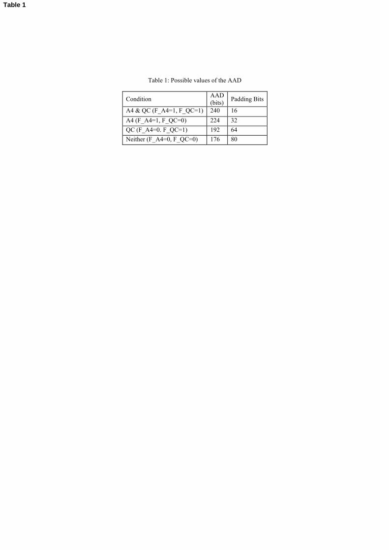
Table 1: Possible values of the AAD
ConditionAAD(bits)
Padding Bits
A4 & QC (F_A4=1, F_QC=1) 240 16
A4 (F_A4=1, F_QC=0) 224 32
QC (F_A4=0. F_QC=1) 192 64
Neither (F_A4=0, F_QC=0) 176 80
Table 1

Table 2: Implementation results of the AESCCMP for three different technologies
Parameter /
Device
AESCCMP
Virtex-4 LX
XC4lX100 -
11
AESCCMP
Virtex-II
XC2V2000-6
AESCCMP
Spartan-3
XC3S4000-5
Period (ns) 6.711 8.483 11.863
Clock(MHz) 149.00 117.88 84.29
Slices 1921 1609 1640
LUTs 3186 2511 2499
BRAM 20 20 20
Throughput (Gbps) 1.876 1.484 1.061
Power Consumption (mW) 1022 618 746
Table 2

Table 3: Implementation results of the AES-CCMP hardware architectures
Work-Device
FPGA
resources
(Slices,
BRAM)
Clock
frequency
(MHz)
Throughput
(Gbps)
Efficiency
Mbps/Slices
Efficiency
Mbps/MHz
[10] – Spartan-3 523 63.70 0.127 0.243 1.993
[11] – VirtexE 3750 50.00 0.243 0.064 4.860
[12] – Virtex-II 3474,
15 BRAM
80.30 0.275 0.079
3.424
[13] – Stratix 5605 logic
cells
50.00 0.285
0.052 Gbps/
logic cells
5.700
[14] – ASIC
module
- - 0.054 - -
[15] – Processor - 66.00 0.275 - 4.166
[16] – Processor - 1500.00 > 2 - 1.333
This work –
Virtex4-LX
1921,
20 BRAM
149.00 1.876 0.976
12.590
This work –
Virtex-II
1609,
20 BRAM
117.88 1.484 0.922
12.589
This work –
Spartan-3
1640,
20 BRAM
84.29 1.061 0.646
12.587
Table 3

Fig. 1. Security architecture based on the AES-CCM Protocol for IEEE 802.11i-2004 networks.
Figure 1

Fig. 2. Block diagram of the AES-CCM algorithm.
Figure 2

Fig. 3. Block diagram of the AES-CBC-MAC algorithm.
Figure 3

Fig. 4. Block diagram of the AES-CTR algorithm.
Figure 4

Fig. 5. Block diagram of the AES algorithm.
Figure 5

Fig. 6. Block diagram of the AESCCMP architecture.
Figure 6

Fig. 7. Block diagram of the AESCCM module.
Figure 7

Fig. 8. Block diagram of the AES_Cipher component.
Figure 8

(a) (b)
(c)
(d)
Fig. 9. Block diagram of the modules: (a) Format_N&Q, (b) Format_AAD, (c) Format_Payload, and (d) Format_CB.
Figure 9

Fig. 10. AAD Construction [2].
Figure 10

(a)
(b)
Figure 11

(c)
Fig. 11. Finite State Machines used for control units: (a) Control_FormatAAD, (b) Control_FormatPayload,
and (c) Control_FormatCB.

|
Fig. 12. Finite State Machine used in the Control_CCMP sub-module.
Figure 12
Related Documents