Abstract—The decoding of Downlink Control Information (DCI) in LTE is based upon a process that is defined as a blind decoding which depends on a number of decoding attempts on a number of Physical Downlink Control Channel (PDCCH) candidate locations for a number of defined DCI formats. In this paper, two proposed designs for DCI decoder are presented. The first decodes based upon monitoring PDCCH candidate locations serially. This design can perform the whole 44 decoding attempts within 87.3 % of the whole OFDM symbol time with extended cyclic prefix. So, it's well suited for Multicast/Broadcast over Single Frequency Network (MBSFN) subframes. However, this design doesn't meet the worst-case time of an LTE OFDM symbol with normal cyclic prefix. Therefore, a second design is proposed that exploits parallelism to enable fast blind decoding process. The proposed parallel design proves efficiency in meeting decoding time constraints besides, consuming a little power with a proven efficiency in utilization area perspective. The proposed parallel design performs all of 44 decoding attempts in a time of 7.8 μs which is only 11.7 % of an LTE useful OFDM symbol time with a logic power consumption of only 17000 μW. The proposed designs are simulated using Modelsim 6.4a and implemented in Plan Ahead 14.4 in 28 nm technology, Virtex7 FPGA kit of part number XC7V2000T, which is characterized by high performance and large capacity. Index Terms—LTE, UESSS, CSS, DCI, PDCCH, UE. I. INTRODUCTION Long Term Evolution (LTE) is a fourth generation wireless high speed broadband technology developed by the third generation partnership project (3GPP) to provide high data rates, low latency, high mobility, reduced costs and compatibility with existing systems besides packet- optimized radio access technology supporting flexible bandwidth deployments [1]. The increasing demands of today’s user poses a challenge in the design of recent communication systems like 3GPP LTE to perform fast processing of user data. Fast processing of user data requires reliable delivery of the data and the associated control signaling that specifies the format of the data and the location and timing of the radio resources allocated to the user. To accomplish high data rates, the LTE standard requires the usage of instantaneous adaptive Manuscript received July 10, 2013; revised September 3, 2013. Mohamed S. Abo Zeid, Mohamed E. Nasr, and Salah El Deen A. Khamis are with Electronics and Electrical Communications Dept., Faculty of Engineering, Tanta University, Tanta and 31527, Egypt (e-mail: [email protected], [email protected], mnasr@f- eng.tanta.edu.eg). Khaled M. Elsayed is with Electronics and Electrical Communications Dept., Faculty of Engineering, Cairo University, Giza and 12613, Egypt (e- mail: author@lamar. colostate.edu). modulation and coding techniques to accommodate the channel quality conditions [2]. However, this poses a challenge of proper signaling of these adaptive parameters to the UE on a separate control channel which results in increasing the channel bandwidth required for signaling and hence reducing the bandwidth available for the user's traffic [3]. An alternative approach is that the UE is neither informed about its intended DCI format nor its location within the control region of subframe. Therefore, The UE performs a number of decoding attempts to obtain the intended control format. This process is the blind decoding process [4]. Such process has the advantage of reducing the amount of resources needed for control information transmission while simultaneously increasing the reliable delivery of data and control information [5]. The 3GPP LTE specifications define the candidate locations that the UE shall monitor, instead of monitoring all locations within the control region, to reduce the UE power consumption and the timing needed to accomplish that monitoring [6]. These defined set of resources in which each UE shall monitor its control information are called search spaces. The standard of LTE, also, defines two search spaces. UE-Specific Search Space (UESSS) where its candidate locations are monitored by specific UE and it is used for transmission of control information that configures specific UE. On the other hand, Common Search Space (CSS) where its candidate locations are monitored by all UEs in the serving cell and it is used for transmission of common control information for all eNodeB's UEs [7]. In this paper two proposed designs for DCI decoder are presented. The first monitors the PDCCH candidate locations in a serial manner. Although, it is proved efficiency from decoding time perspective with subframes comprising of OFDM symbols with extended cyclic prefixes, it is being verified that it does not meet the worst- case time of an LTE OFDM symbol with normal cyclic prefix. Therefore, a second design is proposed that exploits parallelism to enable fast blind decoding process. The design also has proven efficiency in meeting time requirements of the decoding process and also good utilization area and power efficiency. The rest of the paper is organized as follows. Section II gives information about LTE frame structure. Section III describes the basics of LTE downlink control channels. Section IV deals with blind decoding process. Section V provides the proposed system design model. The serial decoder is presented in section VI while the parallel design is presented in Section VII. In Section VIII results and discussion are provided followed by conclusions in Section IX. Efficient Design and Implementation of LTE Downlink Control Information Decoder Mohamed S. Abo Zeid, Khaled M. Elsayed, Mohamed E. Nasr, and Salah El Deen A. Khamis International Journal of Computer Theory and Engineering, Vol. 6, No. 2, April 2014 160 DOI: 10.7763/IJCTE.2014.V6.856

Welcome message from author
This document is posted to help you gain knowledge. Please leave a comment to let me know what you think about it! Share it to your friends and learn new things together.
Transcript

Abstract—The decoding of Downlink Control Information
(DCI) in LTE is based upon a process that is defined as a blind
decoding which depends on a number of decoding attempts on
a number of Physical Downlink Control Channel (PDCCH)
candidate locations for a number of defined DCI formats. In
this paper, two proposed designs for DCI decoder are
presented. The first decodes based upon monitoring PDCCH
candidate locations serially. This design can perform the whole
44 decoding attempts within 87.3 % of the whole OFDM
symbol time with extended cyclic prefix. So, it's well suited for
Multicast/Broadcast over Single Frequency Network (MBSFN)
subframes. However, this design doesn't meet the worst-case
time of an LTE OFDM symbol with normal cyclic prefix.
Therefore, a second design is proposed that exploits parallelism
to enable fast blind decoding process. The proposed parallel
design proves efficiency in meeting decoding time constraints
besides, consuming a little power with a proven efficiency in
utilization area perspective. The proposed parallel design
performs all of 44 decoding attempts in a time of 7.8 µs which
is only 11.7 % of an LTE useful OFDM symbol time with a
logic power consumption of only 17000 µW. The proposed
designs are simulated using Modelsim 6.4a and implemented in
Plan Ahead 14.4 in 28 nm technology, Virtex7 FPGA kit of
part number XC7V2000T, which is characterized by high
performance and large capacity.
Index Terms—LTE, UESSS, CSS, DCI, PDCCH, UE.
I. INTRODUCTION
Long Term Evolution (LTE) is a fourth generation
wireless high speed broadband technology developed by the
third generation partnership project (3GPP) to provide high
data rates, low latency, high mobility, reduced costs and
compatibility with existing systems besides packet-
optimized radio access technology supporting flexible
bandwidth deployments [1].
The increasing demands of today’s user poses a challenge
in the design of recent communication systems like 3GPP
LTE to perform fast processing of user data. Fast processing
of user data requires reliable delivery of the data and the
associated control signaling that specifies the format of the
data and the location and timing of the radio resources
allocated to the user. To accomplish high data rates, the LTE
standard requires the usage of instantaneous adaptive
Manuscript received July 10, 2013; revised September 3, 2013.
Mohamed S. Abo Zeid, Mohamed E. Nasr, and Salah El Deen A.
Khamis are with Electronics and Electrical Communications Dept., Faculty
of Engineering, Tanta University, Tanta and 31527, Egypt (e-mail:
[email protected], [email protected], mnasr@f-
eng.tanta.edu.eg).
Khaled M. Elsayed is with Electronics and Electrical Communications
Dept., Faculty of Engineering, Cairo University, Giza and 12613, Egypt (e-
mail: author@lamar. colostate.edu).
modulation and coding techniques to accommodate the
channel quality conditions [2]. However, this poses a
challenge of proper signaling of these adaptive parameters
to the UE on a separate control channel which results in
increasing the channel bandwidth required for signaling and
hence reducing the bandwidth available for the user's traffic
[3]. An alternative approach is that the UE is neither
informed about its intended DCI format nor its location
within the control region of subframe. Therefore, The UE
performs a number of decoding attempts to obtain the
intended control format. This process is the blind decoding
process [4]. Such process has the advantage of reducing the
amount of resources needed for control information
transmission while simultaneously increasing the reliable
delivery of data and control information [5].
The 3GPP LTE specifications define the candidate
locations that the UE shall monitor, instead of monitoring all
locations within the control region, to reduce the UE power
consumption and the timing needed to accomplish that
monitoring [6]. These defined set of resources in which each
UE shall monitor its control information are called search
spaces.
The standard of LTE, also, defines two search spaces.
UE-Specific Search Space (UESSS) where its candidate
locations are monitored by specific UE and it is used for
transmission of control information that configures specific
UE. On the other hand, Common Search Space (CSS) where
its candidate locations are monitored by all UEs in the
serving cell and it is used for transmission of common
control information for all eNodeB's UEs [7].
In this paper two proposed designs for DCI decoder are
presented. The first monitors the PDCCH candidate
locations in a serial manner. Although, it is proved
efficiency from decoding time perspective with subframes
comprising of OFDM symbols with extended cyclic
prefixes, it is being verified that it does not meet the worst-
case time of an LTE OFDM symbol with normal cyclic
prefix. Therefore, a second design is proposed that exploits
parallelism to enable fast blind decoding process. The
design also has proven efficiency in meeting time
requirements of the decoding process and also good
utilization area and power efficiency.
The rest of the paper is organized as follows. Section II
gives information about LTE frame structure. Section III
describes the basics of LTE downlink control channels.
Section IV deals with blind decoding process. Section V
provides the proposed system design model. The serial
decoder is presented in section VI while the parallel design
is presented in Section VII. In Section VIII results and
discussion are provided followed by conclusions in Section
IX.
Efficient Design and Implementation of LTE Downlink
Control Information Decoder
Mohamed S. Abo Zeid, Khaled M. Elsayed, Mohamed E. Nasr, and Salah El Deen A. Khamis
International Journal of Computer Theory and Engineering, Vol. 6, No. 2, April 2014
160DOI: 10.7763/IJCTE.2014.V6.856

II. LTE FRAME STRUCTURE
LTE supports two frame types FDD and TDD, in this
paper FDD is the adopted one where one LTE radio frame
duration is 10 ms consisting of 10 sub frames, each of 1 ms
duration. Each subframe is divided into two slots, each of
0.5 ms duration which includes seven OFDM symbols for
normal cyclic prefix and six OFDM symbols for extended
cyclic prefix, the FDD frame structure is shown in Fig. 1
[8].
According to LTE specifications, a subcarrier spacing
=15 KHz corresponds to a useful OFDM symbol time =
(1/subcarrier spacing) ≈ 66.7μs is defined [8]. The overall
OFDM symbol time consists of useful OFDM symbol time
plus cyclic prefix time .With normal cyclic prefix the whole
OFDM symbol time is 71.4 µs compared to 83.4 µs with
extended cyclic prefix.
Fig. 1. FDD Frame Structure.
III. LTE CONTROL CHANNEL PRELIMINARIES
The LTE downlink includes 3 physical control channels.
The Physical Control Format Indicator Channel (PCFICH)
carries the Control Format Indicator (CFI) which determines
the number of OFDM symbols (1, 2 or 3 OFDM symbols) in
1 ms sub-frame used for transmission of downlink control
information. Physical Downlink Control Channel (PDCCH)
is the heart of downlink control channels as it carries the
Downlink Control Information (DCI). DCI includes the
uplink scheduling grants and downlink scheduling
assignments [1]. It contains, also, the type of modulation
being used for Physical Downlink Shared Channel
(PDSCH), which carries UE's downlink data, besides other
control information. Physical H-ARQ Indicator Channel
(PHICH) carries the downlink ACK/NACK information
associated with uplink data transmission [9].
The basic building unit of PDCCH is the Control Channel
Element (CCE), where each CCE consists of nine Resource
Element Groups (REGs). Each REG consists of four
physical Resource Elements (REs) with each RE carrying
Quadrature Phase Shift Keying (QPSK) symbol
corresponding to one OFDM symbol and one subcarrier.
Hence, one CCE includes 36 QPSK symbols equivalent to
72 bits [10].
Each PDCCH consists of one CCE or an aggregation of
CCEs. CCEs aggregation is a form of repetition coding. In
accordance to LTE specifications, there are only four
aggregation levels supported. So, four PDCCH formats one
for each CCE aggregation level as shown in Table I are
defined [11]. CCEs are consecutively used and numbered in
sequence. The total number of CCEs in the control region of
sub-frame depends on the bandwidth of the system and the
aggregation level being used for transmission of control
information which depends exactly on the channel condition
experienced by the UE [12].
TABLE I: LTE PDCCH FORMATS
PDCCH
FORMATs
LTE PDCCH FORMATS
No. of CCEs
No.
of REGs
No. of PDCCH bits
0
1
2
3
1
2
4
8
9
18
36
72
72
144
288
576
Each PDCCH carries DCI. Different DCI formats are
supported in LTE. Each of these DCI formats contains the
minimum payload required for a particular scenario which
reduces the signaling overhead. The supported DCI formats
are shown in Table II [11].
TABLE II: LTE DCI FORMATS
DCI
Format
DCI Format Purpose
0
1
1A
1B
1C
1D
2
2A
3&3A
Used for scheduling of PUSCH
Transmission of assignments of PDSCH
Compact scheduling of PDSCH
PDSCH assignments for rank 1 transmission
Used for very compact transmission of PDSCH
Used for compact signaling of PDSCH assignments
for multi-user MIMO.
PDSCH assignments for closed loop MIMO
operation.
PDSCH assignments for open loop MIMO
operation.
Transmit power control commands for multiple
users for PUCCH and PUSCH with 2-bits and 1-bit
power adjustments, respectively.
The LTE standard defines that the number of control
information bits of each DCI format depends mainly on the
assigned downlink resource blocks (DL Bandwidth) and
uplink resource blocks (UL Bandwidth). They typically
obtained from transmission of basic system information on
broadcast channel (BCH). The standard also, defines that
DCI formats 0, 1A, 3 and 3A have the same payload size of
control information bits [5].
IV. THE LTE PDCCH BLIND DECODING PROCESS
In PDCCH blind decoding process, the UE using UE-
Specific Search Space (UESSS), from Table III, shall
monitor 6 PDCCH candidate locations in aggregation level
1 (L=1), and 6 PDCCH candidate locations in aggregation
level 2, in addition to, 2 PDCCH candidate locations in L=4
and L=8. So, a total of 16 PDCCH candidate locations shall
be monitored in case of UESSS. The UE shall attempt to
decode all DCI formats in these candidate locations which
would pose strict challenges on timing constraints and
power usage. However, 3GPP LTE specifications define that
each UE may receive only 2 DCI formats per Transmission
Time Interval (TTI) of 1 ms. One reference DCI format is
always to be received which is DCI format 0/1A. As 0/1A
DCI formats have the same payload size of control
information bits with one flag bit for differentiation between
International Journal of Computer Theory and Engineering, Vol. 6, No. 2, April 2014
161

them so, only one blind decoding attempt is required for
decoding them per PDCCH candidate location [10]. In
addition to that attempt, one more decoding attempt per
PDCCH candidate location for one of other DCI formats 1,
1B, 1D, 2, 2A is needed where only one of them every TTI
is assigned to the UE. This DCI format is corresponding to
the configured transmission mode that is signaled from
higher layer (RRC signaling) to the UE. Hence, In the
UESSS, a total of 16×2=32 blind decoding attempts are
required to monitor all PDCCH candidate locations for the
assigned two DCI format types per TTI.
TABLE III: LTE SEARCH SPACES [7]
Search
Space
Type
LTE Search Spaces
Aggregation
level
(L)
Size [in
CCEs]
Number of
PDCCH Candidates
UESSS
1
2
4
8
6
12
8
16
6
6
2
2
CSS
4
8
16
16
4
2
As indicated in Table III, for Common Search Space
(CSS), PDCCH candidate locations are defined in
aggregation levels 4 and 8 only. For L=4, there are 4
PDCCH candidate locations, and for L=8 only 2 PDCCH
candidate locations are defined. So, in total, 6 blind
decoding attempts to monitor all candidate locations for
Common Search Space are needed. The UE monitors in
Common Search Spaces DCI formats 0, 1A, 3, 3A and 1C.
Since DCI formats 0/1A and 3/3A have the same payload
size, one blind decoding attempt per PDCCH candidate
location is needed to decode them. Additionally, one more
decoding attempt is, also, needed per PDCCH candidate
location for DCI format 1C which is used for scheduling of
broadcast control information which includes paging,
random access response and system information block
transmissions [5]. As a result, total of 6×2 =12 blind
decoding attempts are used to check all PDCCH candidate
locations for the 2 DCI formats assigned every TTI for the
Common Search Space. As a consequence of that a total of
12+32= 44 blind decoding attempts are required to monitor
all PDCCH candidate locations in both the CSS and UESSS
for the assigned DCI formats every TTI.
According to LTE specifications, The UE monitors only
one CSS at each of the aggregation levels 4 and 8 and one
UESSS at each of the aggregation levels 1, 2, 4, 8. The
UESSS and CSS may overlap [7].
V. SYSTEM DESIGN MODEL
Fig. 2 shows the block diagram of LTE DCI encoder at
eNodeB. The DCI control information bits are firstly,
appended with 16 cyclic redundancy check (CRC) parity
bits for error detection purposes. Also, to save additional
payload, the resultant 16 CRC parity bits are masked the
Radio Network Temporary Identifier (RNTI) of the
particular intended UE .This will also help to check if this
DCI is intended to that UE or not. After that, the resultant
DCI bits with the 16 appended RNTI masked CRC bits
undergo tail-biting convolutional coder (TBCC) with rate
1/3 and constraint length of 7 [13]. A rate matching block is
then used to obtain the desired code rate. Finally, PDCCH
candidate locations defined from UESSS for particular UE
and CSS are determined to place these DCI formats in
appropriate candidate locations with the desired code rate.
Fig. 3 shows the reverse process for these operations at the
UE.
Fig. 2. Block Diagram of LTE DCI Encoder.
Fig. 3. Block Diagram of LTE DCI Decoder.
The procedure for blind decoding process performed at
the UE can be summarized as shown in Fig. 4.
Fig. 4. Design model flow chart.
DCI
Encoded ….. DCI …
PDCCHs
Multiplexing &
CCEs Aggregation
16 bits
CRC
UEID
Masking
TBCC
R=1/3
Rate
matching
Encoded
DCI
Decoded DCI
Defining
PDCCH
Candidate
sets
De-Rate
matchin
g
Viterbi
Decoding
UEID
De-Masking
CRC Check
International Journal of Computer Theory and Engineering, Vol. 6, No. 2, April 2014
162
VI. THE PROPOSED SERIAL DESIGN
The Proposed serial design consists of a chain of
functional blocks each of it is performing a specific function
in the blind decoding process as shown in the following
sections.
A. Defining PDCCH Candidate Locations
The PDCCH candidate locations are defined in terms of
CCEs using UE-Specific Search Space and Common Search
Space hashing functions as shown in (1) [12]:
,mod /k k cce k
S L L Y m N L i
(1)
1 modk kY A Y D (2)
Sk(L) is UESSS of sub-frame k at aggregation level L
where L ∈ {1, 2, 4, 8} and i = 0, 1, 2, ... , L − 1.
N(cce,k) is the total number of CCEs in the control region of
sub-frame k and m = 0, 1, 2, …. , M (L), where M (L) is the
number of monitored PDCCH candidates in the given search
space corresponding to aggregation level L [12], as shown in
Table III.
Yk is given from (2) where A=39827, D=65537 and k=
(ns/2) where ns is the slot number within a radio frame. Y-1 is
initially assigned with the Radio Network Temporary
Identifier (RNTI) of the intended UE.
Sk(L) is also, the hashing function for CSS of sub-frame k
at aggregation level L where L ∈ {4, 8} and i = 0, 1, ... , L
− 1, provided that Yk is set to 0 for only these two
aggregation levels L=4 and L=8 [7].
B. Clocked RAM
The objective of this RTL block is to select the PDCCH
bits from each of the defined PDCCH candidate locations at
each of the aggregation levels for both UESSS and CSS. It
also, provides a memory to store the selected bits from the
multiplexed PDCCHs bits train and after finishing blind
decoding process of each of PDCCH candidate locations,
the selected bits of the second PDCCH candidate location
are provided for the decoding process. This will be
performed at every positive edge of the assigned clock
frequency. Hence, its name is clocked RAM.
C. De-Rate Matcher
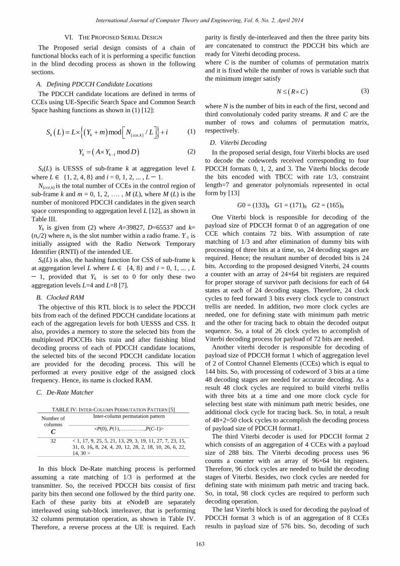
TABLE IV: INTER-COLUMN PERMUTATION PATTERN [5]
Number of
columns
C
Inter-column permutation pattern
<P(0), P(1),…………..,P(C-1)>
32
< 1, 17, 9, 25, 5, 21, 13, 29, 3, 19, 11, 27, 7, 23, 15,
31, 0, 16, 8, 24, 4, 20, 12, 28, 2, 18, 10, 26, 6, 22,
14, 30 >
In this block De-Rate matching process is performed
assuming a rate matching of 1/3 is performed at the
transmitter. So, the received PDCCH bits consist of first
parity bits then second one followed by the third parity one.
Each of these parity bits at eNodeB are separately
interleaved using sub-block interleaver, that is performing
32 columns permutation operation, as shown in Table IV.
Therefore, a reverse process at the UE is required. Each
parity is firstly de-interleaved and then the three parity bits
are concatenated to construct the PDCCH bits which are
ready for Viterbi decoding process.
where C is the number of columns of permutation matrix
and it is fixed while the number of rows is variable such that
the minimum integer satisfy
N R C (3)
where N is the number of bits in each of the first, second and
third convolutionaly coded parity streams. R and C are the
number of rows and columns of permutation matrix,
respectively.
D. Viterbi Decoding
In the proposed serial design, four Viterbi blocks are used
to decode the codewords received corresponding to four
PDCCH formats 0, 1, 2, and 3. The Viterbi blocks decode
the bits encoded with TBCC with rate 1/3, constraint
length=7 and generator polynomials represented in octal
form by [13]
G0 = (133)8 G1 = (171)8 G2 = (165)8
One Viterbi block is responsible for decoding of the
payload size of PDCCH format 0 of an aggregation of one
CCE which contains 72 bits. With assumption of rate
matching of 1/3 and after elimination of dummy bits with
processing of three bits at a time, so, 24 decoding stages are
required. Hence; the resultant number of decoded bits is 24
bits. According to the proposed designed Viterbi, 24 counts
a counter with an array of 24×64 bit registers are required
for proper storage of survivor path decisions for each of 64
states at each of 24 decoding stages. Therefore, 24 clock
cycles to feed forward 3 bits every clock cycle to construct
trellis are needed. In addition, two more clock cycles are
needed, one for defining state with minimum path metric
and the other for tracing back to obtain the decoded output
sequence. So, a total of 26 clock cycles to accomplish of
Viterbi decoding process for payload of 72 bits are needed.
Another viterbi decoder is responsible for decoding of
payload size of PDCCH format 1 which of aggregation level
of 2 of Control Channel Elements (CCEs) which is equal to
144 bits. So, with processing of codeword of 3 bits at a time
48 decoding stages are needed for accurate decoding. As a
result 48 clock cycles are required to build viterbi trellis
with three bits at a time and one more clock cycle for
selecting best state with minimum path metric besides, one
additional clock cycle for tracing back. So, in total, a result
of 48+2=50 clock cycles to accomplish the decoding process
of payload size of PDCCH format1.
The third Viterbi decoder is used for PDCCH format 2
which consists of an aggregation of 4 CCEs with a payload
size of 288 bits. The Viterbi decoding process uses 96
counts a counter with an array of 96×64 bit registers.
Therefore, 96 clock cycles are needed to build the decoding
stages of Viterbi. Besides, two clock cycles are needed for
defining state with minimum path metric and tracing back.
So, in total, 98 clock cycles are required to perform such
decoding operation.
The last Viterbi block is used for decoding the payload of
PDCCH format 3 which is of an aggregation of 8 CCEs
results in payload size of 576 bits. So, decoding of such
International Journal of Computer Theory and Engineering, Vol. 6, No. 2, April 2014
163

code words require a total of 192 decoding stages. So, the
number of clock cycles required up to obtaining the decoded
output sequence is 194 clock cycles .This format is the worst
case to decode with this large amount of time required for
just Viterbi decoding process. This time is repeated serially
4 times where 4 PDCCH candidate locations are defined in
PDCCH format 3. Two locations for each of UESSS and
CSS are defined.
Also, in the proposed Viterbi design, a clock gating
technique which allows only the trace-back block to be
switched on after finishing of the processing of the entire
received codewords. Besides, the use of counter with clock
gating technique allows only one 64 bits register of the
memory array for storing survivor path decision for each
state to be on at a time. These methods in designing will
result in reducing the dynamic power dissipation which is an
important concern for saving the limited UE battery power.
E. UEID De-Masking
After performing the Viterbi decoding of received
PDCCH format corresponds to PDCCH candidate location
defined from hashing function, UEID de-masking is
performed according to (4) [12]:
mod 2q i b i c i (4)
where b is the 16 bits CRC parity sequence and c is 16 bits
RNTI of the intended UE. As the LTE standard defines that,
3/3A DCI formats are masked with different RNTIs other
than C-RNTI which is used to mask 0/1A DCI formats,
therefore, the UEID is variable in the RTL according to the
required RNTI for De-Masking function.
F. CRC Check
CRC check block is a combinational logic that performs
16 bits CRC check in only one clock cycle to reduce the
total amount of delayed time required for blind decoding
process. Using 16–bits CRC generator polynomial in (5) that
is defined from 3GPP LTE specifications [13]
16 12 5
16 1crcg Z Z Z Z (5)
If the generated CRC parity bits similar to the received
CRC parity bits, So this DCI format assigned to that UE and
saved in memory for performing the required operations on
PDSCH based on its' control field information. Otherwise,
so this DCI format is not intended to that UE or it may be
corruptly received with too many errors. In both cases, this
payload is neglected and not being considered.
VII. THE PROPOSED PARALLEL DESIGN
In the proposed parallel design, the basic blocks of the
proposed serial design are used with some modifications in
designing of these blocks, especially, Viterbi blocks which
are the heart of blind decoding process that causes the large
amount of decoding delay in the blind decoding process.
Instead of using a single decoding window which results
in increasing the decoding delay, a high speed Viterbi
processing of the received code words is proposed. It is
based on the technique of sliding window method where the
decoding process considers independent blocks that can be
processed simultaneously in forward and backward
directions [14]. With this method, blocks of data can be
processed independently which causes unlimited
concurrency that results in speeding the decoding process of
long stream of bits within a small amount of time. With the
Viterbi decoding condition of that the decoding window size
must be greater than or equal to five times of constraint
length [15], also, as 3GPP LTE specifications define the
constraint length of TBCC to be 7. So, a decoding window
of 35 stages or greater can be used effectively for decoding
process with negligible decoding performance degradation.
Hence, the Viterbi decoder for PDCCH format 1 can be used
as the basic decoding window for both PDCCH format 2
and PDCCH format 3. For PDCCH format 2 the number of
concurrent block is limited to two, while for PDCCH format
3, a number of 4 concurrent blocks provide an efficient
decoding performance.
Also, the clocked RAM used in parallel design is different
from that of the one used in the proposed serial design.
Parallelism is utilized to speed up the blind decoding
process. The clocked RAM stores only the selected bits for
the first 3 PDCCH candidate locations while other one is
being used to store the selected bits for the remaining 3
PDCCH candidate locations simultaneously. This is the case
for 6 PDCCH candidate locations .While for only 4 PDCCH
candidate locations for PDCCH format 3 which is the basic
part of large decoding delay. One clocked RAM is used to
store the selected bits for only 2 first candidate locations .At
the same time, another one is used for storing the selected
bits for the other 2 PDCCH candidate locations. So, instead
of performing one decoding attempt at a time, with this
method two decoding attempts are performed
simultaneously at a time.
Also, the PDCCH candidate locations for UESSS are
treated independently of the CSS candidate locations thus
achieving parallelism in their decoding.
VIII. RESULTS AND DISCUSSION
A. Proposed Serial Design Simulation Results
The resultant simulation of the proposed serial search
design is shown in Fig. 5, while Fig. 6 shows its Register
Transfer Logic (RTL) diagram. The variable 'CLK' is the
input port for the assigned clock frequency; 'UEID' is the C-
RNTI for the UE which performs blind decoding to search
for its assigned DCI formats. In the simulation, it is assigned
to 14. Variable 'ncce' is input indicating the number of CCEs
in the control region used for estimating clocked RAM
which stores PDCCH bits of PDCCH format 1. CLK4 is
assigned for clocked RAM storing of bits of PDCCH format
2. Finally, CLK8 for RAM that PDCCH candidate locations
(UESSS - CSS hashing functions). In the simulation, it is
assigned to 20. 'TTI' is the input port of sub-frame number.
'PDCCHs' is also an input port for the received train of
PDCCHs bits. ' res_UESS_com' is the input port for
resetting to the initial state after every a complete blind
decoding process. As shown from Fig. 5, CLK11, CLK2,
CLK4, CLK8 are obtained from dividing the clock
frequency assigned to the system for providing serially, the
bits of every PDCCH candidate location, after completing
International Journal of Computer Theory and Engineering, Vol. 6, No. 2, April 2014
164

the previously decoded candidate one. CLK11 is the
assigned clock for clocked RAM storing PDCCH bits of
PDCCH format 0. While CLK2 is assigned for stores
PDCCH bits of PDCCH format 3. As being stated, it's the
slowest one since the large decoding delay of single
decoding window. The first two check variables are
'Check1dci1', 'Check1dci2' which are output ports for
indicating whether there are DCI formats (DCI1, DCI2), for
each PDCCH decoded candidate of PDCCH format 0,
intended for the UE or not. If there are, so check with logic
0 is resulted and the correctly decoded DCI bits are stored in
a memory which its size depends on the length of the
decoded DCI bits. These two check variables in the
simulation waveform followed by 'Check2dci1',
'Check2dci2', 'Check4dci1', 'Check4dci2', 'Check8dci1' and
'Check8dci2', respectively. These check variables indicate
whether there are DCI formats (DCI1, DCI2) for each
PDCCH decoded candidate of PDCCH format 1, format 2
and format 3, respectively, intended for the UE or not. It's
cleared from the simulation waveform, when 'check1dci1'
indicates zero logic so, a successful decoding attempt is
resulted and the monitored PDCCH payload is intended to
the UE. The variable 'originalctrl_bits1DCI1' stores these
DCI bits of PDCCH of format 0, and it can be clearly
noticed that this action is synchronized with 'CLK11' cycle.
Also, the stored DCI bits are changed every clock cycle of
CLK11 based on the blindly decoding of the monitored
PDCCH candidate. The same operation occurs with
PDCCHs of formats 1, 2 and 3.
Fig. 5. Simulation output of the proposed serial design.
Fig. 6. RTL Diagram of the proposed serial design。
B. Timing Calculation of the Proposed Serial Design
The maximum operating frequency resulted from the
synthesis report for the proposed serial search design is
10.565 MHz which is equivalent to a minimum clock period
of 94.649 ns. As previously mentioned, for the system to
perform 44 blind decoding attempts, it must search for the
four candidate locations of PDCCH format 3 which consists
of an aggregation level of 8 CCEs with a total of PDCCH
received bits of 576 bits. So, the total number of clock
cycles required to complete one blind decoding of one
candidate location of PDCCH format 3 is 194 clock cycles
for Viterbi decoding plus one clock cycle for CRC checking.
With minimum clock period of 94.649 ns. So the total time
required for one blind decoding attempt of PDCCH format 3
is 94.649 ns × 195 = 18456.555 ns = 18.4 µsec. From
UESSS and CSS, the total number of PDCCH candidate
locations for PDCCH format 3 is 4 (2 candidate locations
for UESSS and 2 for CSS). So a total of 4 decoding attempts
will be performed for PDCCH format 3. So, 4 times of the
computed period for serially processing each of PDCCH
candidates are needed.
As a result, the total period of time required to complete
all of blind decoding attempts for PDCCH format 3 is 18.4
µs × 4 = 73.6 µsec. With this computed time to accomplish
all of 44 blind decoding attempts and with the LTE defined
International Journal of Computer Theory and Engineering, Vol. 6, No. 2, April 2014
165

useful OFDM useful symbol time of 66.7 µsec, the proposed
serial search design is not time efficient at all. As the time
required to perform all of 44 blind decoding attempts is
110.3 % of useful OFDM symbol time which is more than
one OFDM symbol time. However, it can perform the whole
44 decoding attempts within 87.3 % of the whole OFDM
symbol time (useful OFDM symbol time + extended cyclic
prefix time) which makes it an efficient design for decoding
of only MBSFN sub-frames with extended cyclic prefixes.
C. Utilization Area and Power Consumption of the
Proposed Serial Design
The resultant proposed serial design is synthesized and
implemented on virtex7 FPGA kit of part number
XC7V2000T. The utilization area report is shown in Fig. 7.
The power consumption of the Register Transfer Logic
(RTL) is estimated using Xilinx Power Estimator (XPE).
The basic part of power consumption is the dynamic power
which depends heavily on the switching activity. The
consumed dynamic power is 30000 µW with only 2% of
them for logic power while the remaining part is consumed
from clocking activity, as shown in Fig. 8.
Fig. 7. FPGA virtex7 utilization area report.
Fig. 8. Total on-chip power.
As shown from Fig. 8, The leakage power is 495000 µW,
while the core dynamic power is only 6 % of total on chip
power of 531000 µW under the temperature constraints that.
The power consumed from IO ports is 6000 µw. The logic
power is only 12000 µW while clock power is 18000 µW,
as shown from Fig. 9.
Fig. 9. Power consumption of clock, logic and IO.
Fig. 10. Simulation output of the proposed parallel design.
Fig. 11. RTL Diagram of the proposed parallel design.
International Journal of Computer Theory and Engineering, Vol. 6, No. 2, April 2014
166

D. Proposed Parallel Design Simulation Results
The resultant simulation waveform is shown in Fig.10. In
the simulation, different PDCCH train bits are assumed with
each of it 2 different DCI formats are assumed. Also,
Different PDCCH formats are assumed for testing, as seen
some times DCI bits of PDCCH format 0 are obtained. In
other times, DCI bits of PDCCH format 1 are resulted.
The variable 'CLK' is the input port for the assigned clock
frequency. 'Ueid' is the input port for assigning C-RNTI of
the intended UE. It can be any RNTI assigned to UE. 'Ncce'
is also, an input port for assigning the number of Control
Channel Elements (CCEs) of the assigned control region
within the subframe. 'TTI' is the sub-frame number and it's
assigned to zero. 'PDCCHs' is the input port for placing the
received PDCCHs train bits as whole on it .It can be
variable for any number of bits. 'Res_uess_com' is the reset
input port for assigning the initial assignments to each of
ports. 'check6DCI1', 'check6DCI2' are output ports for
indicating whether DCI control bits pass CRC check or not
for the assumed DCI1 and DCI2 respectively, for each of
PDCCH candidate location of PDCCH format 0.
'check32DCI1' is an output port for indicating for each of
the first 3 PDCCH candidate locations of PDCCH format 1,
determined from UESSS hashing function, whether the
assumed DCI format 0/1A intended for UE or not. While
'check62DCI1' is an output port for indicating for each of
the rest of 3 PDCCH candidate locations of PDCCH
format1.
Whether the assumed DCI format pass CRC check or not.
'Check32DCI2' is an output port for indicating for each of
the first 3 PDCCH candidate locations of PDCCH format 2,
determined from UESSS hashing function, whether the
assumed second DCI format, which depends on the
configure transmission mode (RRC signaling), is intended
for the UE or not. 'Check62DCI2' is an output port for CRC
checking that is used for indication of the second DCI
format for each of the rest of PDCCH candidate locations of
PDCCH format 2. 'check4DCI1', 'check4DCI2' are output
ports for defining whether DCI formats, that are transmitted
using PDCCH format 2, are intended to the UE or not.
'Check8DCI1', 'Check8DCI2' are also output ports for
indicating whether DCI formats, that are transmitted using
PDCCH format 3, are intended to the UE or not.
Also, 'check4DCI1_common', 'check4DCI2_common' are
output ports for CRC checking whether DCI formats
transmitted using PDCCH format 2 in the first 2 PDCCH
candidate locations, defined from CSS hashing function, to
the UE or not. 'check4DCI1_common3',
'check4DCI2_common3' are output ports for checking of the
rest of PDCCH candidate locations of PDCCH format 2 in
CSS.
Finally,'check8DCI1_common','check8DCI2_common'
are the two last output ports for checking of any of DCI
formats in the 2 PDCCH candidate locations of PDCCH
format 3 defined from CSS hashing function. The remaining
variables are internal signals defined in the RTL.
'original6ctrl_bits22DCI1' is the signal port of the designed
memory that stores the CRC checked control bits of DCI
format intended to the UE. These DCI bits are obtained from
the second half of PDCCH candidate locations of PDCCH
format 1. The remaining shown variables are internal signals
of the designed memory to look in, if CRC check of any
PDCCH candidate location indicates logic zero.
As shown from simulation, when 'check6dci1' indicates
zero logic, it means successful decoding attempt and the
DCI bits are stored in the internal signal
'original6ctrl_bitsDCI1'.As shown, it changed every change
in the logic contained of 'check6dci1' that is depends on the
result of decoding attempt.
E. Timing Calculation of the Proposed Parallel Design
As the maximum frequency resulted from the synthesis
report for the proposed parallel design is 21.407 MHz which
is the inverse of the minimum clock period of 46.715 ns.
The time required for blindly decoding of one PDCCH
candidate of PDCCH format 3 is 46.715 ns ×51 = 2382.465
ns = 2.3 µs. The proposed design blindly decodes each of
PDCCH candidate locations for the two assumed DCI
formats, simultaneously. Hence, one more PDCCH
candidate needs to be checked for the two DCI formats. So,
the total time required for blindly decoding of PDCCH
candidates of PDCCH format 3 is only 2.3 µs × 2 = 4.6 µs.
This is the total required time to blindly decode PDCCH
candidate locations of PDCCH format 3 defined from
UESSS-CSS hashing functions. In similar manner, for
PDCCH candidates of PDCCH format 2, defined from
UESSS hashing function, the required time to accomplish
the blind decoding process of 2 candidate locations of
PDCCH format 2 is 4.6 µs. Similarly, for PDCCH candidate
locations, defined from CSS hashing function, the required
time is 4.6 µs to accomplish the blind decoding process.
This is resulted from dividing the monitoring process into
two parts; each of it is responsible for decoding only two
PDCCH candidate locations.
While, for PDCCH candidates which defined from
UESSS of PDCCH format 1, there are 6 PDCCH candidate
locations. In the proposed design, they are divided into two
parts performing the blind decoding process concurrently.
Each part blindly decodes only 3 PDCCH candidate
locations. With Viterbi decoder that is designed for PDCCH
format 1, the required number of clock cycles is 51 clock
cycles. With minimum clock period of 46.715 ns, so, for one
blind decoding of each of PDCCH candidates of PDCCH
format 1, a time of 2.3 µs is required. So, a total of 2.3 µs ×
3 = 6.9 µs is required for blind decoding of all of 3 PDCCH
candidate locations of PDCCH format 1 which is an
aggregation of 2 CCEs.
For PDCCH candidates of PDCCH format 0 which is an
aggregation of one CCE with payload size of 72 bits. So, the
total number of clock cycles needed to accomplish Viterbi
decoding process are 26 clock cycles ,in addition to one
more clock cycle for CRC check .Hence, the total time
required for blindly decoding of one candidate location is
46.715 ns × 27 =1261.305 ns ≈ 1.3 µs. With blind decoding
of the assumed two DCI formats per PDCCH candidate at a
time and, 6 PDCCH candidates locations, the total time for
the complete blind decoding attempts is 1.3 µs × 6 = 7.8 µs.
As a result, depending on these calculation, a time of 7.8
µs which is equivalent to approximately of 11.7% of one
LTE useful OFDM symbol time is required to accomplish
the 44 blind decoding attempts and determines if there are
International Journal of Computer Theory and Engineering, Vol. 6, No. 2, April 2014
167

DCI formats intended to the UE or it goes into micro sleep
to save the limited battery power.
F. Utilization Area and Power Consumption of the
Proposed Parallel Design
The resultant proposed parallel design is synthesized and
implemented on virtex7 FPGA kit of part number
XC7V2000T which is characterized by low power and large
capacity. As shown from utilization area report in Fig. 12,
the number of fully used LUT–FF pairs for the proposed
parallel design is increased by only 1744 pairs compared to
the proposed serial design.
Fig. 12. Utilization area report of proposed parallel design.
The consumption power of the RTL is estimated using
Xilinx Power Estimator (XPE) tool, as shown in Fig. 13.
Fig. 13. Total on-chip power of proposed parallel design.
From Fig. 13, the leakage power is 495000 µw of total
on-chip power, while the dynamic power is 44000 µw which
is equivalent to only 8 % of total on-chip power. The logic
power is only 3 % of total on-chip power which is
equivalent to 17000 µw, while clock power is 26000 µw.
The leakage, clock, logic and IO power consumption are
shown in Fig. 14.
Fig. 14. Power consumption of clock, logic and IO.
IX. CONCLUSIONS
Two designs of LTE DCI decoder are proposed in this
paper. The proposed designs are simulated using Modelsim
and implemented in Virtex7 FPGA kit. The proposed serial
design is proved efficiency in decoding DCI associated with
MBSFN subframes with extended cyclic prefixes, as a
consequence of completing the blind decoding process
within 87.3 % of the whole OFDM symbol time. The
proposed serial design is failed to meet the worst-case time
of an LTE OFDM symbol with normal cyclic prefix. The
proposed parallel design is presented and proved better
performance in decoding time of DCI for all subframes. The
proposed parallel design is proved efficiency of
accomplishing 44 blind decoding attempts within a time of
7.8 µs, which is only 11.7 % of an LTE useful OFDM
symbol time, with a logic power consumption of 17000 µW
by increasing of only 5000 µw compared to the proposed
serial design. It is, also, proved efficiency in the occupied
utilization area of Virtex7 FPGA kit.
REFERENCES
[1] L. Jialing, R. Love, K. Stewart, and M. E. Buckley, "Design and
Analysis of LTE Physical Downlink Control Channel," in Proc.
Vehicular Technology Conference 2009, VTC Spring 2009, IEEE
69th, 2009, pp. 1-5.
[2] J. Eriksson, R. Moosavi, and E. G. Larsson, "Complexity reduction of
blind decoding schemes using CRC splitting,” in Proc. IEEE Global
Telecommunications Conference (GLOBECOM), 2012.
[3] F. Capozzi, D. Laselva, F. Frederiksen, J. Wigard, I. Z. Kovács, and
P. E. Mogensen, "UTRAN LTE downlink system performance under
realistic control channel constraints," in Proc. Vehicular Technology
Conference Fall (VTC 2009-Fall), 2009 IEEE 70th, 2009, pp. 1-5.
[4] D. P. Malladi, J. Montojo, and S. Sarkar, "Methods and systems for
PDCCH blind decoding in mobile communications," United States
Patent Application Publication 2009/0168922, Jul. 2, 2009.
[5] R. T. Love, J. liu, V. Nangia, and R. Nory, "Control channel
provisioning and signaling," Ed: WO Patent 2,010,129,400, 2010.
[6] M. Lauridsen, A. R. Jensen, and P. Mogensen, "Fast control channel
decoding for LTE UE power saving," in Proc. Vehicular Technology
Conference (VTC Spring), 2012 IEEE 75th, 2012, pp. 1-5.
[7] 3GPP TS 36.213, Evolved Universal Terrestrial Radio Access
(EUTRA); Physical Layer Procedures (Release 8).
[8] E. Dahlman, S. Parkvall, J. Skold, and P. Beming, 3G Evolution:
HSPA and LTE for Mobile Broadband, Academic Press, 2010, ch. 16,
pp. 352-362.
[9] S. J. Thiruvengadam and L. M. A. Jalloul, "Performance analyis of
the 3GPP-LTE physical control channels," EURASIP Journal on
Wireless Communications and Networking, vol. 2010, pp. 914-934,
Nov. 2010.
[10] E. Dahlman, S. Parkvall, and J. Skold, 4G: LTE/LTE-Advanced for
Mobile Broadband, Academic Press, 2011,ch. 10, pp. 195-200.
[11] Balamurali, "Optimal downlink control channel resource allocation
for LTE systems," in Proc. 2010 International Conference on Signal
Processing and Communications (SPCOM), 2010, pp. 1-5.
[12] F. Khan, LTE for 4G Mobile Broadband: Air Interface Technologies
and Performance, Cambridge University Press, 2009, ch. 15 ,pp. 390-
396.
[13] 3GPP TS 36.212, Evolved Universal Terrestrial Radio Access
(EUTRA); Multiplexing and Channel Coding (Release 8).
[14] M. Vestias, H. Neto, and H. Sarmento, "Sliding block viterbi decoders
in FPGA," in Proc. 2012 22nd International Conference on Field
Programmable Logic and Applications (FPL), 2012, pp. 595-598.
[15] M. Vestias and H. Sarmento, "Tradeoffs in the design of sliding block
Viterbi decoders for MB-OFDM UWB systems," in Proc. 2012 IEEE
International Conference on Consumer Electronics-Berlin (ICCE-
Berlin), 2012, pp. 173-177.
Mohamed S. Abo Zeid received his B.Sc. (honors) in
Electrical Engineering from Tanta University in 2009.
He is currently a teaching assistant in Electronics and
Electrical Communications department in Faculty of
Engineering, Tanta University.
International Journal of Computer Theory and Engineering, Vol. 6, No. 2, April 2014
168

Mohamed E. Nasr received his Ph.D. in Digital
Communications Engineering from Delhi University in
1985 and his M.Sc. in Electrical Communications
Engineering from Mansoura University in 1979 and
B.Sc. (honors) in Computer Engineering from
Menoufia University in 1975.
He is currently a professor of Wireless
Communications in Tanta University. He was the head
of Electronics and Electrical Communications department in Faculty of
Engineering, Tanta University from 2004 to 2008.
Salah El Deen A. Khamis received his Ph.D. in
Wireless Communications Engineering from Moscow
Academy in 1992 and his M.Sc. in Communications
Engineering from Menoufia University in 1985 and
B.Sc. (honors) in Electrical Engineering from Cairo
University in 1977.
He is currently an associate professor of Wireless
Communications in Tanta University, the head of Electronics and
Electrical Communications department in Faculty of Engineering, Tanta
University.
International Journal of Computer Theory and Engineering, Vol. 6, No. 2, April 2014
169
Related Documents