arXiv:1310.4805v1 [cond-mat.mes-hall] 17 Oct 2013 Efficient and realistic device modeling from atomic detail to the nanoscale J. E. Fonseca · T. Kubis · M. Povolotskyi · B. Novakovic · A. Ajoy · G. Hegde · H. Ilatikhameneh · Z. Jiang · P. Sengupta · Y. Tan · G. Klimeck Received: date / Accepted: date Abstract As semiconductor devices scale to new di- mensions, the materials and designs become more de- pendent on atomic details. NEMO5 is a nanoelectron- ics modeling package designed for comprehending the critical multi-scale, multi-physics phenomena through efficient computational approaches and quantitatively modeling new generations of nanoelectronic devices as well as predicting novel device architectures and phe- nomena. This article seeks to provide updates on the current status of the tool and new functionality, in- cluding advances in quantum transport simulations and with materials such as metals, topological insulators, and piezoelectrics. Keywords nanoelectronics · Greens function formal- ism (NEGF) · NEMO · tight-binding · quantum dot · strain · transport and phonons · Poisson · parallel computing 1 Introduction Relentless downscaling of transistor size has continued according to Moores law for the past 40 years. Transis- tor size will continue to decrease in the next ten years, but foundational issues with currently unknown tech- nology approaches must be pursued [1]. This downscal- ing has reached the range where the number of atoms in critical dimensions is countable, geometries are formed in three dimensions and new materials are being intro- J. E. Fonseca Network for Computational Nanotechnology Purdue Univer- sity West Lafayette, Indiana, US Tel.: 1765-496-6495 E-mail: [email protected] G. Klimeck E-mail: [email protected] duced. Under these conditions we argue that the over- all geometry constitutes a new material that cannot be found as such in nature [2]. Quantum effects such as tunneling, state quantization, and atomistic disorder dominate the characteristics of these nano-scale devices. The interactions of electrons, photons, and phonons are now governed by these new material properties and long-range interactions such as strain and gate fields. The end-game of the transistor size down-scaling as we know it is now fundamentally in sight. The end-game transistor is expected to be about 5nm long and 1nm in its critical active region corresponding to about 5 atoms in width. The physical atomistic down-scaling limit will be reached in about 8-10 years. The overall agenda is to bridge ab initio materials science into TCAD simula- tions of realistically large scaled devices and get macro- scopic quantities like current, voltages, absorption, etc., by mapping ab initio into basis sets of lower order and include them in a formalism that allows for trans- port. The NEMO5 nanoelectronics modeling software is aimed at comprehending the critical multi-scale, multi- physics phenomena and delivering results to engineers, scientists, and students through efficient computational approaches and quantitatively modelling new genera- tions of nanoelectronic devices in industry, as well as predicting novel device architectures and phenomena. The basic functionality and history of the NEMO tool suite has been discussed previously [3,4]. NEMO5’s general software framework can easily include any kind of atomistic model and even semi-classical models if necessary. The scalable software implements Schr¨o- dinger’s equation and non-equilibrium Green’s func- tion method (NEGF) in tight-binding formalism, for electronic structure and transport calculations, respec- tively. It also is able to take into account important effects such as atomistic strain, using valence force field

Welcome message from author
This document is posted to help you gain knowledge. Please leave a comment to let me know what you think about it! Share it to your friends and learn new things together.
Transcript

arX
iv:1
310.
4805
v1 [
cond
-mat
.mes
-hal
l] 1
7 O
ct 2
013
Efficient and realistic device modeling from atomic detail tothe nanoscale
J. E. Fonseca · T. Kubis · M. Povolotskyi · B. Novakovic · A. Ajoy ·
G. Hegde · H. Ilatikhameneh · Z. Jiang · P. Sengupta · Y. Tan · G.
Klimeck
Received: date / Accepted: date
Abstract As semiconductor devices scale to new di-mensions, the materials and designs become more de-
pendent on atomic details. NEMO5 is a nanoelectron-
ics modeling package designed for comprehending the
critical multi-scale, multi-physics phenomena through
efficient computational approaches and quantitativelymodeling new generations of nanoelectronic devices as
well as predicting novel device architectures and phe-
nomena. This article seeks to provide updates on the
current status of the tool and new functionality, in-cluding advances in quantum transport simulations and
with materials such as metals, topological insulators,
and piezoelectrics.
Keywords nanoelectronics · Greens function formal-
ism (NEGF) · NEMO · tight-binding · quantum dot ·
strain · transport and phonons · Poisson · parallelcomputing
1 Introduction
Relentless downscaling of transistor size has continued
according to Moores law for the past 40 years. Transis-
tor size will continue to decrease in the next ten years,but foundational issues with currently unknown tech-
nology approaches must be pursued [1]. This downscal-
ing has reached the range where the number of atoms in
critical dimensions is countable, geometries are formed
in three dimensions and new materials are being intro-
J. E. FonsecaNetwork for Computational Nanotechnology Purdue Univer-sity West Lafayette, Indiana, US Tel.: 1765-496-6495E-mail: [email protected]
G. KlimeckE-mail: [email protected]
duced. Under these conditions we argue that the over-all geometry constitutes a new material that cannot
be found as such in nature [2]. Quantum effects such
as tunneling, state quantization, and atomistic disorder
dominate the characteristics of these nano-scale devices.
The interactions of electrons, photons, and phononsare now governed by these new material properties and
long-range interactions such as strain and gate fields.
The end-game of the transistor size down-scaling as we
know it is now fundamentally in sight. The end-gametransistor is expected to be about 5nm long and 1nm in
its critical active region corresponding to about 5 atoms
in width. The physical atomistic down-scaling limit will
be reached in about 8-10 years. The overall agenda is
to bridge ab initio materials science into TCAD simula-tions of realistically large scaled devices and get macro-
scopic quantities like current, voltages, absorption, etc.,
by mapping ab initio into basis sets of lower order
and include them in a formalism that allows for trans-port. The NEMO5 nanoelectronics modeling software is
aimed at comprehending the critical multi-scale, multi-
physics phenomena and delivering results to engineers,
scientists, and students through efficient computational
approaches and quantitatively modelling new genera-tions of nanoelectronic devices in industry, as well as
predicting novel device architectures and phenomena.
The basic functionality and history of the NEMO
tool suite has been discussed previously [3,4]. NEMO5’s
general software framework can easily include any kindof atomistic model and even semi-classical models if
necessary. The scalable software implements Schro-
dinger’s equation and non-equilibrium Green’s func-
tion method (NEGF) in tight-binding formalism, forelectronic structure and transport calculations, respec-
tively. It also is able to take into account important
effects such as atomistic strain, using valence force field

2 J. E. Fonseca et al.
(VFF) strain models. It then allows the calculation of
electronic band structures, charge density, current and
potential, eigen-energies and wave-functions, phonon
spectra, etc., for a large variety of semiconductor ma-
terials and devices.
This manuscript seeks to provide interested read-
ers with an overview of the recent developments sur-
rounding NEMO5. This paper discusses approaches a)to quantum transport solutions, b) newly-implemented
approaches to achieve faster convergence in the self-
consistent Poisson-transport solution, c) strain, d)
phonons, e) semi-automated material parameterization,f) metals, g) piezoelectric materials such as SmSe, h)
topological insulators and i) band structure unfolding.
2 Transport
At the heart of NEMO5’s quantum transport ap-
proach is the non-equilibrium Green’s function method(NEGF) which is a computational approach to han-
dle quantum transport in nanoelectronic devices [5].
NEGF is numerically expensive when applied on atom-
istic tight-binding representations. NEGF requires stor-
age, inversion and multiplication of matrices of the or-der of the number of electronic degrees of freedom. A
well known method to ease the numerical burden is the
recursive Greens function method (RGF) that allows
for limiting the calculation and storage of the retardedGreens function to specific matrix blocks (such as only
block diagonals and a single block column). Until re-
cently, the RGF algorithm was limited to quasi 1D
transport regimes, i.e. devices with 2 leads only. Gen-
eralizing work of Cauley et al., however, shows thatRGF can be applied on virtually any transport prob-
lem, if the device Hamiltonian matrix is partitioned in
a proper way [6]. NEMO5 allows partitioning the device
ideally for 1D and quasi 1D transport problems accord-ing to the transport coordinate, but it also allows for
the partition of complex, multi terminal devices and the
application of RGF on them.
Despite the RGF method, the computational bur-
den in memory and CPU time is still limiting the max-
imum device size solvable with NEGF. To overcome
this obstacle, NEMO5 offers incomplete spectral trans-
formations of NEGF equations into a Hilbert space ofsmaller rank than the original tight-binding represen-
tation [7]. Special cases of this low rank approxima-
tion are known as CBR method (all ballistic NEGF) [8]
and the mode space approach [9]. This method allowsapproximating NEGF transport problems in electronic
tight-binding representations within a fraction of the
numerical load of exact NEGF solutions. The loss of the
Fig. 1 Comparison of the electron density of the exactNEGF calculation (circle) and of NEGF calculations with10% of the original matrix rank.
NEGF accuracy and predictive power is thereby negli-
gible as shown in Fig. 1 This figure compares the con-
duction band electron density of a homogeneous 5x5nmSi nanowire in equilibrium calculated in an exact and
a LRA-approximate NEGF calculation where the rank
has been reduced down to 10% of the original prob-
lem size. Negligible discrepancies are magnified in the
figure’s inset.
Purely ballistic charge transport can be well de-scribed within the quantum transmitting boundary
method (QTBM) [10]. Since this method solves the
quantum transport in the space of propagating lead
modes, the numerical load is typically much smallerthan in ballistic NEGF or RGF calculations which in
general consider all modes. NEMO5 is able to solve
the QTBM equations spatially distributed over large
numbers of CPUs. For a given energy and transverse
momentum, the boundary equations of the source andthe drain are solved each on individual CPUs, whereas
those sections of the device that are not in direct con-
tact with the leads are solved on the remaining CPUs.
3 Self-consistent calculation
The many-body problem is treated in the Hartree ap-
proximation by self-consistently solving the Poisson andtransport equations (e.g. QTBM, as explained above).
The self-consistent solution is a nonlinear problem and
any efficient solution of this problem must take into ac-
count at least three components: the energy grid, theinitial guess, and the self-consistent algorithm. The en-
ergy grid should resolve the features in the energy de-
pendent device charge density, determined by the lead

Efficient and realistic device modeling from atomic detail to the nanoscale 3
density of states and device transmission properties. A
good energy grid should be inhomogeneous, so that it
is able to resolve sharp features, yet have as few energy
points as possible to facilitate efficient computations.
Since the self-consistent process is necessarily iterativein nature, the initial guess is the first step in the so-
lution. A good initial guess, close to the final solution,
can prevent convergence problems. The self-consistent
algorithm provides the next potential guess in each iter-ation. Ideally, the algorithm should prevent divergence
and arrive at the solution with as few as possible iter-
ations. Via PETSc, NEMO5 employs several kinds of
Newton-Raphson algorithms [11], that rely on an effi-
cient and approximate Jacobian implementation [12,13]and have protection against divergence by being able to
control the potential update, or step size, between two
iterations. The Newton-Broyden method and trust re-
gion methods [14] are also used. While robust, thesemethods do not always guarantee efficient solutions.
We achieve the most efficient solutions by construct-
ing an accurate and time-efficient initial guess, based
on the semi-classical charge and locally constant Fermi
level with the effective mass corrected for confinementeffects, followed by the Newton-Raphson method with
full step size.
Results of one self-consistent simulation using the
tight-binding formalism in NEMO5 are shown in Fig.
2. The simulated device is n-type Si nanowire with 3x3nm cross section (approximately 3 nm). The wire has 1
nm thick gate all-around and three doping regions: the
channel under the gate is doped to 1015 cm−3, while
the source and drain regions to 1020 cm−3. The lengthof the simulated device is 20 nm, of which 10 nm is the
channel and 5 nm the source and drain regions each.
The source and drain region length is chosen so that
the potential becomes flat near the lead-device inter-
face. Results are shown in Fig. 2. The simulation is per-formed up to 0.6 V gate bias, to avoid unphysical effects
at higher bias produced by ballistic transport in the
absence of the transport barrier and subsequent Pois-
son/transport equation convergence issues. The conver-gence scheme consists of the Newton-Raphson method
with full step size and the following initial guesses: for
the first bias point the semi-classical initial guess is
used; for the second bias point the previous solution
is used as the initial guess; and for the third bias pointupward the prediction/extrapolation based on the pre-
vious two solutions. This convergence scheme takes a
total of 27 iterations for the 7 bias points simulated.
The majority of inner bias points took only 3 itera-tions, while the first and the last bias point resulted in
a slightly higher number of iterations. Even though the
semi-classical initial guess with the effective mass cor-
rected for confinement effects is very close to the final
solution, the fact that the spatial effects of the confine-
ment (i.e. quantum wave function) are not taken into
account results in slightly more iterations. On the other
hand, the quality of the semi-classical guess protects thesimulation from divergence, as the full step size is used.
The last bias point takes slightly more iterations, due to
the fact that it is more difficult to achieve convergence
for diminishing transport barrier at high gate bias.
4 Strain
In the last decade, strain was a major performance
booster in ultra-scaled transistors [15] and it is of fun-damental importance to consider the effect of strain
on the band-structure and transport properties of
novel devices. Heterostructures composed of lattice mis-
matched materials exhibit strain intrinsically. As shownin Fig. 3 NEMO5 is able to compute strain and relax
the atomistic heterostructures using the Enhanced Va-
lence Force Field (EVFF) [16,17,18]. The energy func-
tional contains not only Keating terms such as bond-
stretching and bond-bending interactions, but alsocross-stretching, stretch-bending, and second-nearest-
neighbor angle-angle interactions. For polar materials,
the long-range Coulomb interaction can be added in
the case of 0-D (bulk) and 3-D (confined) simulations.NEMO5 contains two strategies for elastic energy min-
imization. One uses Jacobian and Hessian matrices
and can be used only for small structures. The sec-
ond method is approximate and is based only on the
Jacobian.
5 Phonons
Nanowires show excellent thermo-electric properties
which make them favorable for thermo-electric devices.For example silicon nanowires exhibit 100 times better
ZT compared to bulk silicon and can achieve maximum
ZT around 1 [19], creating a strong motivation for ac-
curate phonon modeling in nanoscale devices. It is wellknown that the Keating model overstimates phonon
energies of both optical and acoustic branches [18].
NEMO5 is able to calculate phonon dispersion using
the EVFF model which provides a reasonable match
with experimental phonon dispersion (Fig. 4). The dy-namical matrix has been calculated by the following:
Di,jλ,µ =
1√
MiMj
∂2U
∂rλi ∂rµj
e−iq·rij (1)

4 J. E. Fonseca et al.
0 0.1 0.2 0.3 0.4 0.5 0.6
10−10
10−8
10−6
10−4
gate bias Vg [V]
Ids
[A]
a
0 10 20
−1
−0.5
0
position along wire [nm]
Bul
k ba
nd e
dge
[eV
]
b
Vg=0VVg=0.2VVg=0.4VVg=0.6V
0 10 200
5
10
15x 10
20
position along wire [nm]
Ele
ctro
n de
nsity
[cm
−3 ]
c
Fig. 2 NEMO5 self-consistent simulation results for n-typeall-around gate Si nanowire. The gate length is 10 nm, whilethe doping in the channel below the gate is 1015 cm−3. Thesource and drain regions are taken to be 5 nm with 1020 cm−3
doping. Panel a) shows the current-voltage characteristic, b)is the bulk band edge interpolated along the center of thenanowire, and c) is the same for electron density. The chargedensity is nonuniform in the cross section due to lateral quan-tum confinement and significantly larger than the convergedaverage charge which equals the doping. The simulation had7 voltage points and took in total 27 Poisson/transport equa-tion iterations, thanks to an efficient convergence scheme.
Fig. 3 Strain simulation in a Nitride Hetero-structureNanowire using NEMO5. (a) Physical structure and dimen-sions, (b) plot of strain component ezz which shows long rangediffusion of strain.
in which i and j are atom indexes, λ and µ can be oneof x, y or z directions, qis the phonon wave vector, Mi
and Mj are atom masses for atom i and j respectively
and U is the total elastic energy of the system.
6 Metal insulator transition - SmSe
With shrinking physical dimensions, the total transistor
number in a single chip has been increasing exponen-tially for each generation. However, the scaling of the
supply voltage in Silicon based MOSFET is limited by
the 60mV/dec subthreshold swing (SS). The desire to
reduce heat dissipation drives research for devices withdifferent switching mechanisms. [20]
The Piezoelectronic Transistor (PET) [21,22] is a
promising approach to achieve a high ON/OFF ratiowith very small voltage swing. In PET, the gate voltage
is transduced to acoustic waves through a buffer layer
made with piezoelectric (PE) materials. The channel
layer of piezoresistive (PR) materials, e.g. Samariummonochalcogenides, is capable of modifying the con-
ductance by several orders of magnitude subjected to
moderate strain [23] which is generated by deforma-
Efficient and realistic device modeling from atomic detail to the nanoscale 5
Fig. 4 Phonon dispersion of Si calculated by EVFF modelusing NEMO5 vs. experiment.
tion of PE. When the dimensions of PET are reduced
to the nanometer scale, the device performance will be
dominated by quantum effects. Quantum confinement
will change band structure and minimum leakage isdetermined by tunneling. To simulate devices of real-
istic dimensions, computationally efficient models like
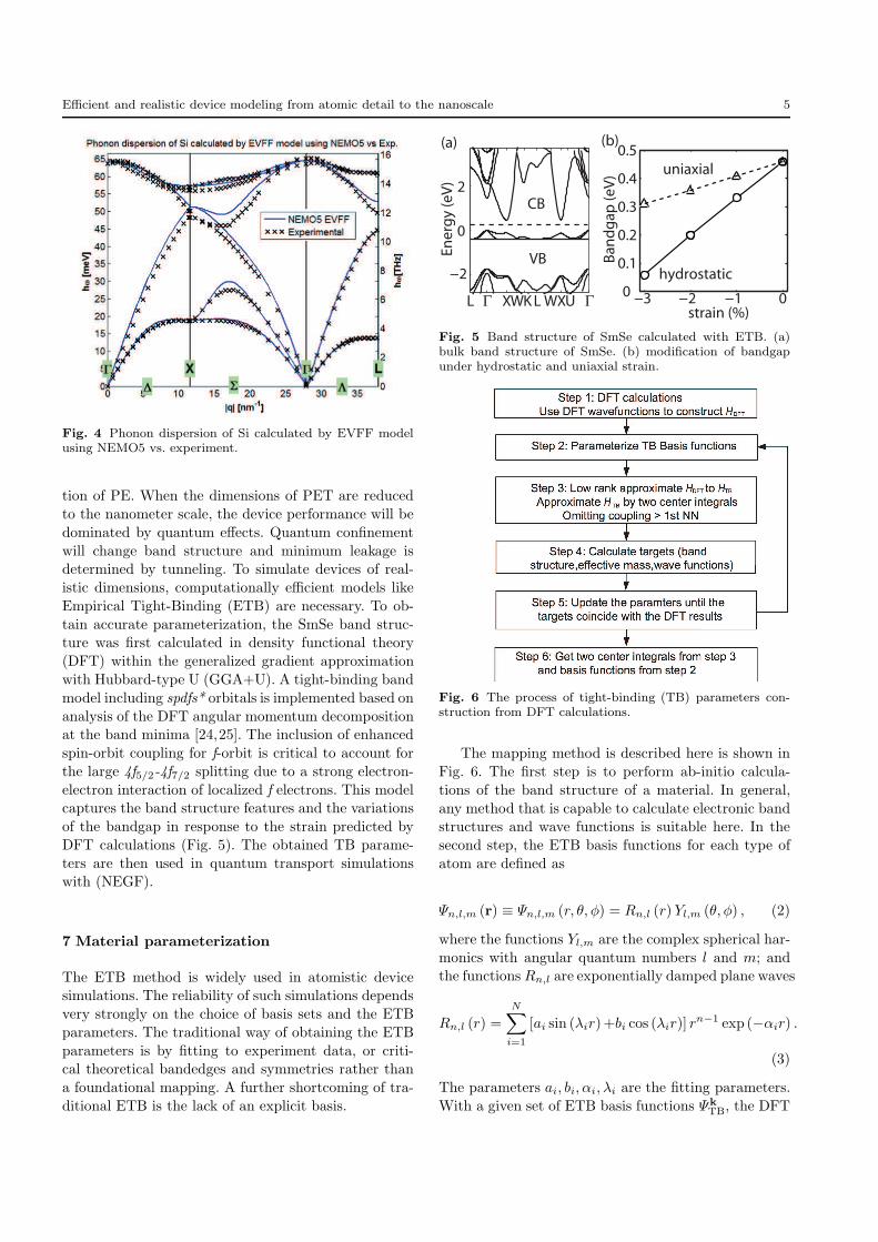
Empirical Tight-Binding (ETB) are necessary. To ob-
tain accurate parameterization, the SmSe band struc-ture was first calculated in density functional theory
(DFT) within the generalized gradient approximation
with Hubbard-type U (GGA+U). A tight-binding band
model including spdfs* orbitals is implemented based on
analysis of the DFT angular momentum decompositionat the band minima [24,25]. The inclusion of enhanced
spin-orbit coupling for f-orbit is critical to account for
the large 4f5/2-4f7/2 splitting due to a strong electron-
electron interaction of localized f electrons. This modelcaptures the band structure features and the variations
of the bandgap in response to the strain predicted by
DFT calculations (Fig. 5). The obtained TB parame-
ters are then used in quantum transport simulationswith (NEGF).
7 Material parameterization
The ETB method is widely used in atomistic devicesimulations. The reliability of such simulations depends
very strongly on the choice of basis sets and the ETB
parameters. The traditional way of obtaining the ETB
parameters is by fitting to experiment data, or criti-cal theoretical bandedges and symmetries rather than
a foundational mapping. A further shortcoming of tra-
ditional ETB is the lack of an explicit basis.
L Γ XWKLWXU Γ
−2
0
2
Energy (eV)
−3 −2 −1 00
0.1
0.2
0.3
0.4
0.5
strain (%)
Bandgap (eV)
uniaxial
hydrostaticVB
CB
(a) (b)
Fig. 5 Band structure of SmSe calculated with ETB. (a)bulk band structure of SmSe. (b) modification of bandgapunder hydrostatic and uniaxial strain.
Fig. 6 The process of tight-binding (TB) parameters con-struction from DFT calculations.
The mapping method is described here is shown in
Fig. 6. The first step is to perform ab-initio calcula-
tions of the band structure of a material. In general,
any method that is capable to calculate electronic bandstructures and wave functions is suitable here. In the
second step, the ETB basis functions for each type of
atom are defined as
Ψn,l,m (r) ≡ Ψn,l,m (r, θ, φ) = Rn,l (r) Yl,m (θ, φ) , (2)
where the functions Yl,m are the complex spherical har-
monics with angular quantum numbers l and m; andthe functions Rn,l are exponentially damped plane waves
Rn,l (r) =
N∑
i=1
[ai sin (λir)+bi cos (λir)] rn−1 exp (−αir) .
(3)
The parameters ai, bi, αi, λi are the fitting parameters.
With a given set of ETB basis functions ΨkTB
, the DFT

6 J. E. Fonseca et al.
−20
−10
0
10
20
30
L Γ X W K L W X K Γ
Ene
rgy
(eV
)
DFT
TB Mapping
0 1 2DOS
Fig. 7 Band structure and density of states of MgO by DFTand TB.
Hamiltonian is transformed to the tight-binding rep-
resentation. Any non-zero off-diagonal element of the
overlap matrix is neglected. The ETB Hamilton matrixelements are approximated by two center integrals ac-
cording to the Slater-Koster table [26,27]. ETB Hamil-
ton matrix elements beyond either 1st or 2nd nearest
neighbor coupling are neglected. In Step 4, the band
edges, effective masses and eigen functions of the Hamil-tonian at high symmetry points are calculated and com-
pared to the corresponding DFT results. The overlaps
of the ETB basis functions are also determined. In the
fifth step, all fitting parameters are adjusted to improvethe agreement of the ETB results with the DFT results
and also to reduce the overlap matrix of the ETB basis
functions to the unity matrix. Steps 2 - 5 are repeated
until the convergence criterion is met. Step 6 requires
to extract the converged ETB basis functions and theETB two center integrals.
The DFT mapping method has been validated in
NEMO5 using Si and GaAs[24]. It is also applied suc-
cessfully to Antimonides and new materials such as
MgO[24], SmSe[25]. MgO cyrstalizes in rock salt struc-
ture. Each oxygen atom has six magnesium atoms as 1stnearest neighbors and twelve oxygen atoms as 2nd near-
est neighbors. MgO is parameterized for a 2nd nearest
neighbor sp3d5s∗ ETB model. Within this model, the
interaction between two oxygen atoms is required toproduce the correct valence bands. It can be seen from
Fig.7 that the ETB band structure matches the DFT
result well within the energies −5 to 15 eV.
8 Tight-binding parameterization of metals
Metals play a significant role in microprocessor oper-
ation. Besides connecting individual transistors, metalvias and interconnects deliver bias current, clock sig-
nals and metal-stacks are used for gate metalliza-
tion. In the existing quantum mechanical atomistic
device-modeling paradigm, metal contacts are used
to set the Fermi levels in the source and drain of
the transistor. Once this is done, the metals are
essentially abstracted out of the usual Schrodinger-
Poisson or NEGF-Poisson solution. Owing to decreas-ing device dimensions, the resistance drop across the
metal-semiconductor contact is becoming an increas-
ingly important issue. Additionally, from an overall
power dissipation perspective, the increase in metalresistivity with decreasing via dimensionality is an
extremely important unsolved problem[1]. Atomistic
modeling of metal grain boundary interfaces, metal
interconnect-liner interfaces and metal-semiconductor
interfaces can provide significant guidance in the designof low-resistivity metal interconnects, liner materials
and metal-semiconductor interfaces with low Schottky-
barrier heights. With these objectives in mind, we have
created accurate and computationally efficient Semi-Empirical Tight-Binding (SETB) models of Metals and
Metal-Semiconductor interfaces suitable for studying
electron transport in the aforementioned, technologi-
cally important systems.
NEMO5 contains tight-binding models that have
been formulated specifically to study the phenomenonof resistivity increase in metals with decreasing in-
terconnect dimensions and electron transport across
metal-semiconductor interfaces. As an example of the
capabilities NEMO5 has in this regard, Fig. 8 showsthe bulk band structure of Cu obtained using an ef-
ficient 1st Nearest-Neighbor SETB representation of
its FCC phase. This band structure is obtained by fit-
ting to LCAO Density Functional Theory (DFT) band-
structure for Cu using the exchange-correlation func-tional of Perdew and Zunger within the Generalized
Gradient Approximation (GGA)[28]. It can be seen
that the tight-binding model reproduces the DFT band
structure accurately. In Fig. 9, the transmission in bulkCu along the [001] direction is computed using SETB
and DFT and the results are compared to each other.
It is evident that our SETB model reproduces the DFT
results extremely accurately in the energy range of in-
terest a few kTs below and above the Fermi level.
9 Topological insulators - Bi2Te3
Topological Insulators (TIs) are a new state of matter
with a bulk insulating gap and metal-like states on the
surface or edge. The surface or edge states which are
described by a linear Dirac Hamiltonian are robust andprotected by time reversal symmetry [29,30]. Topolog-
ical insulators have acquired prominence because they
offer a rich collection of fundamentally new phenomena

Efficient and realistic device modeling from atomic detail to the nanoscale 7
Fig. 8 Bulk band structure of Cu in FCC phase calculatedusing the SETB (dots) formalism and DFT (solid lines). No-tice that our SETB model accurately captures DFT bandstructure features in all energies of interest in electronic trans-port.
Fig. 9 Transmission for a 1 nm cell along the [001] directionin Cu computed using SETB and DFT.
along with a wide array of applications including opto-
electronic THz detectors, spin-polarized contacts, ultra-
fast switches, etc. [31]. Several TI materials are known
to exist at room temperature. Bi2Te3 and Bi2Se3 whichpossess bound surface states (Fig. 10) are well-known
examples.
The unique properties of TIs are attributed to the
linear dispersion of surface states that connect theconduction and valence band together. Further, these
states have their spin locked perpendicular to momen-
tum in-plane. NEMO5 offers the capability to com-
pute the atomistic band structure of bulk and confinedBi2Te3 devices. The undoped Bi2Te3 is a narrow band-
gap quintuple-layered semi-conductor with a rhombo-
hedral crystal structure. The quintuple layer crystal
Fig. 10 The bandstructure of a [100] grown Bi2Te3 quantumwell. The surface states are shown within the boxed region.The conduction and valence bands are connected by a lineardispersion also known as a Dirac cone, depicted within thebox. The color bar denotes the strength of spin-polarization.
Fig. 11 The Fermi-surface of the surface states of Bi2Te3with the distinctive snow-flake structure.
structure is used in a twenty band tight-binding model.All parameters for these calculations were obtained
from a orthogonal tight-binding model with sp3d5s*
orbitals, nearest-neighbor interactions, and spin-orbit
coupling [32]. Additionally, the dispersion is spin-
resolved and conforms exactly to experimentally ob-served spin-polarization (see Fig. 10).
The corresponding Fermi-surface of the surface states
exhibit a peculiar snow-flake structure. NEMO5 pre-
dicts this (Fig. 11), in agreement with experiments [33].
When conduction band and valence bands are con-nected (as in the case of TIs) conduction and valence
bands cannot be unambiguously separated. Since an ac-
curate prediction of device characteristics and material
properties needs charge self-consistent calculations, itis imperative to devise electronic structure calculation
models for materials where an explicit differentiation
between electrons and holes is not possible. NEMO5
8 J. E. Fonseca et al.
introduces the concept of a novel charge self-consistent
full-band atomistic tight-binding method that avoids
usage of holes. Hereby, the model of Andlauer and Vogl
has been extended to atomistic tight-binding [34].
10 Bandstructure unfolding
Semiconductor alloys do not possess translational sym-
metry, owing to a random distribution of atoms. For
example, the cationic sites in AlxGa1−xAs can eitheraccommodate an Al or a Ga atom. Thus semiconduc-
tor alloys cannot, in principle, have an associated band-
structure. Nevertheless, it is common to measure and
use quantities associated with bandstructure (for ex-ample, energy bandgap and effective mass) to design
and analyze devices in these materials. A compromise
between the above two positions is to allow for an ap-
proximate bandstructure of alloys, where each energy
band is broadened as a result of randomness. The su-percell method [35,36] provides a computational frame-
work to perform such a calculation. The essential idea
is to construct a very large supercell which is randomly
populated with atoms. A supercell of say Si0.4Ge0.6would have roughly 40% of atoms being Si, while the
rest being Ge. Periodic boundary conditions are im-
posed on this large supercell, and its energy spectrum
determined (typically at a single K point). The super-
cell is viewed as being made up of fictitious primitivecells called small-cells. The supercell energy spectrum
is finally unfolded onto the small-cell Brillouin zone and
approximate small-cell energy bands determined.
In order to obtain adequate points along a particulardirection n in the small-cell Brillouin zone (say [100],
[110], [111] etc.), it is convenient to work with specially
chosen supercells. Reference [37] describes special rect-
angular, non-primitive unitcells that are used as build-
ing blocks to construct such supercells in NEMO3D [38,39]. This approach has two drawbacks – (i) the non-
primitive unit cell is itself made up of a number of small
cells, requiring an additional unfolding step that is de-
pendent on n; (ii) it cannot be used for materials (likeGaN) which do not have rectangular unit cells. NEMO5
implements a more general approach, based on [40,41]
where the supercell is built by cascading specially cho-
sen primitive cells (which could be non-rectangular).
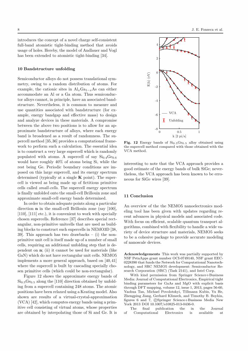
Figure 12 shows the approximate energy bands ofSi0.5Ge0.5 along the [110] direction obtained by unfold-
ing from a supercell containing 248 atoms. The atomic
positions have been relaxed using a Keating model. Also
shown are results of a virtual-crystal-approximation(VCA) [42], which computes energy bands using a prim-
itive cell consisting of virtual atoms, whose properties
are obtained by interpolating those of Si and Ge. It is
0 0.5 1-8
-6
-4
-2
0
2
4
k [2 pi/a]
E(k)(eV)
VCA
Unfolding
Fig. 12 Energy bands of Si0.5Ge0.5 alloy obtained usingthe supercell method compared with those obtained with theVCA method.
interesting to note that the VCA approach provides a
good estimate of the energy bands of bulk SiGe; never-
theless, the VCA approach has been known to be erro-
neous for SiGe wires [39].
11 Conclusion
An overview of the the NEMO5 nanoelectronics mod-
eling tool has been given with updates regarding re-
cent advances in physical models and associated code.
With focus on efficient, scalable quantum transport al-
gorithms, combined with flexibility to handle a wide va-riety of device structure and materials, NEMO5 seeks
to be a cohesive package to provide accurate modeling
of nanoscale devices.
Acknowledgements This work was partially supported byNSF PetaApps grant number OCI-0749140, NSF grant EEC-0228390 that funds the Network for Computational Nanotech-nology, and SRC NEMO5 development: Semiconductor Re-search Corporation (SRC) (Task 2141), and Intel Corp.
With kind permission from Springer Science+BusinessMedia: Journal of Computational Electronics, Empirical tightbinding parameters for GaAs and MgO with explicit basisthrough DFT mapping, volume 12, issue 1, 2013, pages 56-60,Yaohua Tan, Michael Povolotskyi, Tillmann Kubis, Yu He,Zhengping Jiang, Gerhard Klimeck, and Timothy B. Boykin,figures 6 and 7, c©Springer Science+Business Media NewYork 2013 DOI 10.1007/s10825-013-0436-0.
The final publication the in the Journalof Computational Electronics is available at

Efficient and realistic device modeling from atomic detail to the nanoscale 9
http://link.springer.com/article/10.1007%2Fs10825-013-0509-0
References
1. International Technology Roadmap for Semiconductors,2012. http://www.itrs.net.
2. Martin Fuechsle, Jill A. Miwa, Suddhasatta Mahapatra,Hoon Ryu, Sunhee Lee, Oliver Warschkow, Lloyd C. L.Hollenberg, Gerhard Klimeck, and Michelle Y. Simmons.A single-atom transistor. Nat Nano, 7(4):242–246, 2012.10.1038/nnano.2012.21.
3. S. Steiger, M. Povolotskyi, H. H. Park, T. Kubis, andG. Klimeck. Nemo5: A parallel multiscale nanoelectron-ics modeling tool. Ieee Transactions on Nanotechnology,10(6):1464–1474, 2011.
4. Jean Sellier, Jim Fonseca, Tillmann C Kubis, Michael Po-volotskyi, Yu He, Hesameddin Ilatikhameneh, ZhengpingJiang, SungGeun Kim, Daniel Mejia, Parijat Sengupta,and Yaohua Tan. Nemo5, a parallel, multiscale, multi-physics nanoelectronics modeling tool. In SISPAD, 2012.
5. Supriyo Datta. Quantum Transport: Atom to Transistor.Cambridge University Press, Cambridge, 2005.
6. Stephen Cauley, Mathieu Luisier, Venkataramanan Bal-akrishnan, Gerhard Klimeck, and Cheng-Kok Koh. Dis-tributed non-equilibrium green’s function algorithms forthe simulation of nanoelectronic devices with scattering.Journal of Applied Physics, 110(4):043713–14, 2011.
7. Lang Zeng, Yu He, Michael Povolotskyi, XiaoYan Liu,Gerhard Klimeck, and Tillmann Kubis. Low rank ap-proximation method for efficient green’s function calcula-tion of dissipative quantum transport. Journal of Applied
Physics, 113(21):213707–8, 2013.8. D. Mamaluy, M. Sabathil, and P. Vogl. Efficient method
for the calculation of ballistic quantum transport. Jour-
nal of Applied Physics, 93(8):4628–4633, 2003.9. Jing Wang, Eric Polizzi, and Mark Lundstrom. A three-
dimensional quantum simulation of silicon nanowire tran-sistors with the effective-mass approximation. Journal ofApplied Physics, 96(4):2192–2203, 2004.
10. D. Z. Y. Ting, E. T. Yu, and T. C. McGill. Multibandtreatment of quantum transport in interband tunnel de-vices. Physical Review B, 45(7):3583–3592, 1992. PRB.
11. Satish Balay, Jed Brown, Kris Buschelman, William D.Gropp, Dinesh Kaushik, Matthew G. Knepley, Lois Curf-man McInnes, Barry F. Smith, and Hong Zhang. Petscweb page, 2013. http://www.mcs.anl.gov/petsc.
12. A. Trellakis, A. T. Galick, A. Pacelli, and U. Ra-vaioli. Iteration scheme for the solution of the two-dimensional schr[o-umlaut]dinger-poisson equations inquantum structures. Journal of Applied Physics,81(12):7880–7884, 1997.
13. Roger Lake, Gerhard Klimeck, R. Chris Bowen, and De-jan Jovanovic. Single and multiband modeling of quan-tum electron transport through layered semiconductordevices. Journal of Applied Physics, 81(12):7845–7869,1997.
14. Wayne R. Cowell. Sources and development of math-
ematical software. Prentice-Hall series in computa-tional mathematics. Prentice-Hall, Englewood Cliffs,N.J., 1984.
15. D. A. Antoniadis, I Aberg, C. NiChleirigh, O. M. Nayfeh,A. Khakifirooz, and J. L. Hoyt. Continuous mosfet per-formance increase with device scaling: the role of strainand channel material innovations. IBM J. Res. Dev.,50(4/5):363–376, 2006.
16. Sebastian Steiger, Mehdi Salmani-Jelodar, DenisAreshkin, Abhijeet Paul, Tillmann C Kubis, MichaelPovolotskyi, Hong-Hyun Park, and Gerhard Klimeck.Enhanced valence force eld model for the latticeproperties of gallium arsenide. Physical Review B,84(15):155204, 2011.
17. Abhijeet Paul, Mathieu Luisier, and Gerhard Klimeck.Modified valence force field approach for phonon disper-sion: from zinc-blende bulk to nanowires. Journal of
Computational Electronics, 9(3-4):160–172, 2010.18. Zhifeng Sui and Irving P. Herman. Effect of strain on
phonons in Si, Ge, and Si/Ge heterostructures. Physical
Review B, 48(24):17938–17953, 1993. PRB.19. Akram I. Boukai, Yuri Bunimovich, Jamil Tahir-Kheli,
Jen-Kan Yu, William A. Goddard Iii, and James R.Heath. Silicon nanowires as efficient thermoelectric ma-terials. Nature, 451(7175):168–171, 2008. 10.1038/na-ture06458.
20. Thomas N. Theis and Paul M. Solomon. Its time toreinvent the transistor! Science, 327(5973):1600–1601,2010.
21. D.M. Newns, B.G. Elmegreen, X.-H. Liu, and G.J. Mar-tyna. The piezoelectronic transistor: A nanoactuator-based post-cmos digital switch with high speed and lowpower. MRS Bulletin, 37(11):1071–1076, 2012.
22. Dennis M. Newns, Bruce G. Elmegreen, Xiao-Hu Liu,and Glenn J. Martyna. High response piezoelectric andpiezoresistive materials for fast, low voltage switching:Simulation and theory of transduction physics at thenanometer-scale. Advanced Materials, 24(27):3672–3677,2012.
23. N. F. Mott. Metal-insulator transition. Reviews of Mod-
ern Physics, 40(4):677–683, 1968. RMP.24. Yaohua Tan, Michael Povolotskyi, Tillmann C. Kubis,
Yu He, Zhengping Jiang, Gerhard Klimeck, and TimothyBoykin. Empirical tight binding parameters for GaAs andMgO with explicit basis through DFT mapping. Journalof Computational Electronics, 2013.
25. Zhengping Jiang, Marcelo A. Kuroda, Yaohua Tan, Den-nis M. Newns, Michael Povolotskyi, Timothy B. Boykin,Tillmann Kubis, Gerhard Klimeck, and Glenn J. Mar-tyna. Electron transport in nano-scaled piezoelectronicdevices. Applied Physics Letters, 102(19):193501–3, 2013.
26. J. C. Slater and G. F. Koster. Simplified LCAO Methodfor the Periodic Potential Problem. Phys. Rev., 94:1498–1524, Jun 1954.
27. A. V. Podolskiy and P. Vogl. Compact expression for theangular dependence of tight-binding hamiltonian matrixelements. Phys. Rev. B, 69:233101, Jun 2004.
28. John P. Perdew, Kieron Burke, and Matthias Ernzerhof.Generalized gradient approximation made simple. Phys-
ical Review Letters, 77(18):3865–3868, 1996. PRL.29. M. Z. Hasan and C. L. Kane. Colloquium: Topological
insulators. Rev. Mod. Phys., 82:3045–3067, Nov 2010.30. Liang Fu and C. L. Kane. Topological insulators with
inversion symmetry. Phys. Rev. B, 76:045302, Jul 2007.31. Parijat Sengupta, Tillmann Kubis, Yaohua Tan, Michael
Povolotskyi, and Klimeck Gerhard. Design principles forHgTe based topological insulator devices. Journal of Ap-
plied Physics, 114(4):043702, 2013.32. S. Lee and P. von Allmen. Tight-binding modeling of
thermoelectric properties of bismuth telluride. Applied
physics letters, 88:022107, 2006.33. S Souma, K Kosaka, T Sato, M Komatsu, A Takayama,
T Takahashi, M Kriener, Kouji Segawa, and Yoichi Ando.Direct measurement of the out-of-plane spin texture in

10 J. E. Fonseca et al.
the dirac-cone surface state of a topological insulator.Physical Review Letters, 106(21):216803, 2011.
34. Till Andlauer and Peter Vogl. Full-band envelope-function approach for type-ii broken-gap superlattices.Physical Review B, 80(3):035304, 2009. PRB.
35. T.B. Boykin, N. Kharche, G. Klimeck, and M. Korkusin-ski. Approximate bandstructures of semiconductor alloysfrom tight-binding supercell calculations. J. Phys.: Con-
dens. Matter, 19:036203, 2007.36. Voicu Popescu and Alex Zunger. Extracting E versus
k effective band structure from supercell calculations onalloys and impurities. Phys. Rev. B, 85(8):085201, 2012.
37. T.B. Boykin, N. Kharche, and G. Klimeck. Non-primitiverectangular cells for tight-binding electronic structurecalculations. Physica E: Low-dimensional Systems and
Nanostructures, 41(3):490–494, 2009.38. Gerhard Klimeck, Shaikh Shahid Ahmed, Hansang Bae,
Neerav Kharche, Steve Clark, Benjamin Haley, SunheeLee, Maxim Naumov, Hoon Ryu, Faisal Saied, et al.Atomistic simulation of realistically sized nanodevices us-ing NEMO 3-DPart I: Models and benchmarks. IEEE
Trans. Electron Devices, 54(9):2079–2089, 2007.39. Gerhard Klimeck, Shaikh S Ahmed, Neerav Kharche,
Marek Korkusinski, Muhammad Usman, Marta Prada,and Timothy B Boykin. Atomistic simulation of realisti-cally sized nanodevices using NEMO 3-DPart II: Appli-cations. IEEE Trans. Electron Devices, 54(9):2090–2099,2007.
40. PK Aravind. On visualizing crystal lattice planes. Amer-
ican Journal of Physics, 74:794, 2006.41. Arvind Ajoy. Complex bandstructure of direct bandgap
III-V semiconductors: application to tunneling. In 16th
International Workshop on Physics of Semiconductor
Devices, pages 854923–854923. International Society forOptics and Photonics, 2012.
42. A. Paul, S. Mehrotra, M. Luisier, and G. Klimeck. Per-formance Prediction of Ultrascaled SiGe/Si Core/ShellElectron and Hole Nanowire MOSFETs. Electron Device
Letters, IEEE, 31(4):278 –280, 2010.
Related Documents