This content has been downloaded from IOPscience. Please scroll down to see the full text. Download details: IP Address: 165.132.47.78 This content was downloaded on 04/07/2016 at 02:29 Please note that terms and conditions apply. Effects of plasma treatment on surface properties of ultrathin layered MoS 2 View the table of contents for this issue, or go to the journal homepage for more 2016 2D Mater. 3 035002 (http://iopscience.iop.org/2053-1583/3/3/035002) Home Search Collections Journals About Contact us My IOPscience

Welcome message from author
This document is posted to help you gain knowledge. Please leave a comment to let me know what you think about it! Share it to your friends and learn new things together.
Transcript
This content has been downloaded from IOPscience. Please scroll down to see the full text.
Download details:
IP Address: 165.132.47.78
This content was downloaded on 04/07/2016 at 02:29
Please note that terms and conditions apply.
Effects of plasma treatment on surface properties of ultrathin layered MoS2
View the table of contents for this issue, or go to the journal homepage for more
2016 2D Mater. 3 035002
(http://iopscience.iop.org/2053-1583/3/3/035002)
Home Search Collections Journals About Contact us My IOPscience
2DMater. 3 (2016) 035002 doi:10.1088/2053-1583/3/3/035002
PAPER
Effects of plasma treatment on surface properties of ultrathinlayeredMoS2SuhhyunKim1,5,Min SupChoi1,2,5, DeshunQu1,3, ChangHoRa1,3, Xiaochi Liu1,3,MinwooKim1,Young Jae Song1,4 andWon JongYoo1,2,3
1 Department ofNano Science andTechnology, SKKUAdvanced Institute of Nano-Technology (SAINT), SungkyunkwanUniversity,2066, Seobu-ro, Jangan-gu, Suwon, Gyeonggi-do 440-746, Korea
2 Center forHuman InterfaceNanoTechnology (HINT), SungkyunkwanUniversity, 2066, Seobu-ro, Jangan-gu, Suwon, Gyeonggi-do440-746, Korea
3 Samsung-SKKUGrapheneCenter (SSGC), SungkyunkwanUniversity, 2066, Seobu-ro, Jangan-gu, Suwon, Gyeonggi-do 440-746, Korea4 Department of Physics, SungkyunkwanUniversity (SKKU), 2066 Seobu-ro, Jangan-gu, Suwon 440-746, Korea5 These authors contributed equally to this work.
E-mail: [email protected]
Keywords:molybdenumdisulfide, plasma, atomic level etching, doping, work function
Supplementarymaterial for this article is available online
AbstractThis work investigates the use of oxygen plasma (O2) treatment, applied as an inductively coupledplasma, to control the thickness andwork function of aMoS2 layer. Plasma-etchedMoS2 exhibited asurface roughness similar to that of the pristineMoS2. TheMoS2field effect transistors fabricatedusing the plasma-etchedMoS2 displayed a higher n-type doping concentration than that of pristineMoS2. The x-ray photoelectron spectroscopywas performed to analyze chemical composition todemonstrate theminimum level of chemical reactions occurred upon plasma treatment.Moreover,Kelvin probe forcemicroscopymeasurements were conducted to probe the changes in theworkfunction that could be attributed to the changes in the surface potential. Themeasuredwork functionssuggest themodification of a band structure and n-doping effect after plasma treatments thatdepended on the number ofMoS2 layers. This study suggests that theO2 plasma can control the layernumber of theMoS2 aswell as the electronic properties of aMoS2film.
Introduction
The mechanical exfoliation of highly oriented pyroly-tic graphite (HOPG) produces graphene, which has avariety of desirable properties, including a high carriermobility, quantum Hall effects at ambient tempera-tures, and ballistic transport [1, 2]. Although suchproperties have enabled the use of graphene inelectronic devices, graphene devices cannot be turnedoff due to the zero band gap that arises from the lineardispersion relation at the K point [1–3]. Other two-dimensional (2D) layered materials have attractedattention for their sizable band gaps, high current on/off ratios, and high photoresponsivity [4]. Thesematerials may be useful in transparent and flexibleelectronics and optoelectronics [5, 6].
MoS2 is a layered transition metal dichalcogenidethat can be used in semiconductors, catalysts [7], andhydrogen evolution processes [8]. MoS2 layers are
weakly held together by van der Waals forces betweenadjacent layers, and the covalent bonds of the S–Mo–Sstructures are characterized by a large intrinsic bandgap that depends strongly on the number of layers.MoS2 has an indirect band gap of 1.2 eV in the bulkconfiguration; however, single-layerMoS2 transits to adirect band gap of 1.8 eV [9, 10]. An indirect-to-directband gap transition can enhance the photo-effi-ciency [11].
The various researches for controlling thickness ofthe MoS2 film have been conducted, e.g., removal ofMoS2 layers by using low-power argon (Ar) plasma,Raman laser, XeF2 as the gaseous reactant, and ther-mal annealing [12–18]. However, these researchesposed challenges in increased surface roughness andgeneration of unwanted compounds such as MoO3.Capacitively coupled plasma (CCP) etching is a typicaltechnique that damages graphene through the highion bombardment energy of the plasma. A previous
RECEIVED
27 February 2016
REVISED
7 June 2016
ACCEPTED FOR PUBLICATION
21 June 2016
PUBLISHED
1 July 2016
© 2016 IOPPublishing Ltd
study reported that inductively coupled plasma (ICP),unlike CCP, can reduce polymeric residues by clean-ing the graphene, as evidenced by the achievement of asurface roughness similar to that of pristine graphene[19]. For this reason, ICP was used to carefully removelayers of MoS2 while suppressing the reactionsbetween the plasma andMoS2.
In this paper, we investigated the effects of O2
plasma treatment on the MoS2 surface by preciselydesigning a process to control the thickness of MoS2while ensuring that no reactions occurred between theMoS2 and the plasma. X-ray photoelectron spectrosc-opy (XPS) was performed for analyzing the surfacechemistry of a MoS2 film after plasma treatment. Theplasma-treated MoS2 displayed a gradual increase inphotoluminescence (PL) while maintaining a surfaceroughness similar to that of pristineMoS2. In addition,it showed a highly n-doped state after plasma treat-ment displaying a tendency for the Fermi level to beclose to a degenerate level, resulting in a disappearanceof off current. Kelvin probe force microscopy (KPFM)was used to investigate the origin of the high n-typedoping by measuring the surface potential of MoS2.The work functions, which were estimated from themeasured surface potentials of the MoS2 field effecttransistor (FET), were found to depend on the numberof MoS2 layers. These results provide clues to theeffects of the plasma on theMoS2 surface and present apromising approach to obtain single-layered MoS2during the fabrication of 2D material based electronicdevices. This plasma process may be applied in a sim-ple manner at low temperatures without using toxicchemicals to achieve large-scale and low dimensionalMoS2 films.
Experimentalmethods
(A) Device fabrication. Few-layered MoS2 films,mechanically exfoliated from a synthesized bulk 2H-MoS2 purchased at 2D Semiconductors Inc., weretransferred onto a highly p-doped Si substrate coveredwith an oxidized 285 nm SiO2 layer. The thickness andthe surface conditions of the samples were confirmedusing optical microscopy, atomic force microscopy(AFM), and Raman spectroscopy. The Cr/Au (5/50 nm) metal electrodes were formed via electronbeam lithography and evaporation, and the lift-offprocess was performed in an acetone solution over 3 h.The acetone solution was subsequently washed awayusing an isopropyl alcohol (IPA) solution. The lengthand width of the representative devices were 1.8 μmand 3.78 μm, respectively.(B) Plasma treatment. The plasma machine could beoperated under either the ICP or the CCP mode. Weused only the ICP mode to attain a high plasmauniformity and reduce the damage to the MoS2surface. The plasma reactor consisted of a four-turnspiral coil with a 13.56 MHz radio frequency (RF)
power supply and a ceramic dielectric at the top of thechamber. Prior to plasma treatment, an annealingprocess was applied at 250 °C for 3 h using a forminggas (Ar/H2) to remove water and oxygen moleculesfrom the MoS2 flakes. The precise plasma control ofMoS2 layer was achieved by generating an ICPdischarge using O2 gas and varying treating time, at apressure of 200 mTorr, a gas flow rate of 30 sccm, anda power of 21W.(C) Material and electrical characterization. AFM andRaman spectroscopy were carried out to confirm thematerial characteristics of the MoS2 film. Within5 min after plasma treatments, all the measurementswere performed so as to minimize the reactionbetween O2, H2O, and MoS2. The thickness and RMSsurface roughness were measured using AFM, and thefrequency differences were verified via Ramanspectroscopy, measured using a laser wavelength of532 nm. The Raman data were analyzed using theGaussian formula for curve fitting. XPS (ESCALAB205Xi in which x-ray spot size was 900 μm and itslateral resolution was 20 μm) was also performed todetermine the chemical configurations of the bulkMoS2 surface prior to mechanical exfoliation, beforeand after plasma treatment. All electrical measure-ments were conducted using a semiconductor para-meter analyzer at room temperature under vacuumconditions, where drain voltage was fixed at 0.5 V.Photocurrent was measured using a dot laser illumi-nating system with a wavelength of 532 nm and apower intensity of 13 μW. A KPFM analysis wasperformed to understand the surface and electronicstates after O2 plasma had been applied to the MoS2sheet. A gold coated tip bias of 2 V was applied at aresonant frequency of 17 kHz.
Results and discussion
MoS2 layer control usingO2 plasmaWe investigated the atomic level etching ofMoS2 usingO2 plasma regulated via ICP discharge. The etchingconditions were optimized to remove a layer (1L) ofMoS2 including S–Mo–S bonds evenly and minimizethe chemical reaction. Once the atomic-layer etchingmethod had been developed, the MoS2 sample wastreated in 4 s intervals during the total treating time of20 s in an effort to understand how the S–Mo–S bondswere ruptured under a series of brief and divided ICPprocesses.
Firstly, we plasma-treated the pristine MoS2 withthickness of 2.7 nm for total treating time of 20 s with4 s intervals. Figure 1(a) shows the linear decrease inthe thickness of MoS2, as confirmed by AFM. We cal-culated the average thickness from five randomlyselected positions to verify that the surface had beenevenly etched. The average values of these points were2.7, 2.3, 1.9, 1.6, 1.3 and 1.0 nm for 0, 4, 8, 12, 16 and20 s plasma treating time, respectively. The adsorption
2
2DMater. 3 (2016) 035002 SKim et al
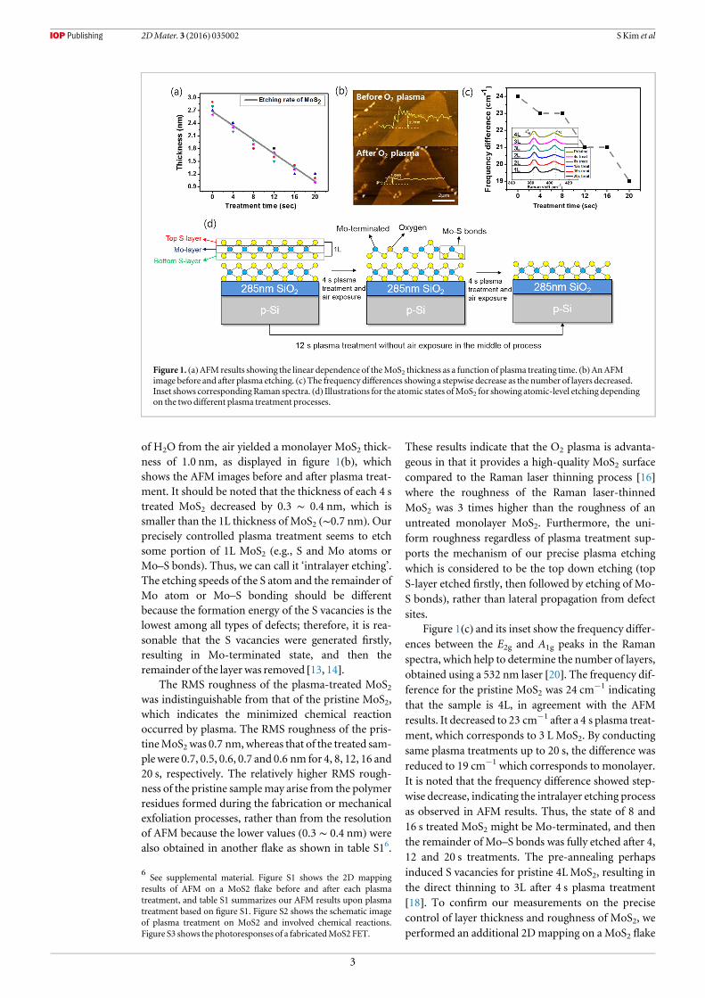
of H2O from the air yielded a monolayer MoS2 thick-ness of 1.0 nm, as displayed in figure 1(b), whichshows the AFM images before and after plasma treat-ment. It should be noted that the thickness of each 4 streated MoS2 decreased by 0.3 ∼ 0.4 nm, which issmaller than the 1L thickness of MoS2 (∼0.7 nm). Ourprecisely controlled plasma treatment seems to etchsome portion of 1L MoS2 (e.g., S and Mo atoms orMo–S bonds). Thus, we can call it ‘intralayer etching’.The etching speeds of the S atom and the remainder ofMo atom or Mo–S bonding should be differentbecause the formation energy of the S vacancies is thelowest among all types of defects; therefore, it is rea-sonable that the S vacancies were generated firstly,resulting in Mo-terminated state, and then theremainder of the layer was removed [13, 14].
The RMS roughness of the plasma-treated MoS2was indistinguishable from that of the pristine MoS2,which indicates the minimized chemical reactionoccurred by plasma. The RMS roughness of the pris-tineMoS2was 0.7 nm,whereas that of the treated sam-ple were 0.7, 0.5, 0.6, 0.7 and 0.6 nm for 4, 8, 12, 16 and20 s, respectively. The relatively higher RMS rough-ness of the pristine samplemay arise from the polymerresidues formed during the fabrication or mechanicalexfoliation processes, rather than from the resolutionof AFM because the lower values (0.3 ∼ 0.4 nm) werealso obtained in another flake as shown in table S16.
These results indicate that the O2 plasma is advanta-geous in that it provides a high-quality MoS2 surfacecompared to the Raman laser thinning process [16]where the roughness of the Raman laser-thinnedMoS2 was 3 times higher than the roughness of anuntreated monolayer MoS2. Furthermore, the uni-form roughness regardless of plasma treatment sup-ports the mechanism of our precise plasma etchingwhich is considered to be the top down etching (topS-layer etched firstly, then followed by etching of Mo-S bonds), rather than lateral propagation from defectsites.
Figure 1(c) and its inset show the frequency differ-ences between the E2g and A1g peaks in the Ramanspectra, which help to determine the number of layers,obtained using a 532 nm laser [20]. The frequency dif-ference for the pristine MoS2 was 24 cm
−1 indicatingthat the sample is 4L, in agreement with the AFMresults. It decreased to 23 cm−1 after a 4 s plasma treat-ment, which corresponds to 3 L MoS2. By conductingsame plasma treatments up to 20 s, the difference wasreduced to 19 cm−1 which corresponds to monolayer.It is noted that the frequency difference showed step-wise decrease, indicating the intralayer etching processas observed in AFM results. Thus, the state of 8 and16 s treated MoS2 might be Mo-terminated, and thenthe remainder of Mo–S bonds was fully etched after 4,12 and 20 s treatments. The pre-annealing perhapsinduced S vacancies for pristine 4LMoS2, resulting inthe direct thinning to 3L after 4 s plasma treatment[18]. To confirm our measurements on the precisecontrol of layer thickness and roughness of MoS2, weperformed an additional 2D mapping on a MoS2 flake
Figure 1. (a)AFMresults showing the linear dependence of theMoS2 thickness as a function of plasma treating time. (b)AnAFMimage before and after plasma etching. (c)The frequency differences showing a stepwise decrease as the number of layers decreased.Inset shows corresponding Raman spectra. (d) Illustrations for the atomic states ofMoS2 for showing atomic-level etching dependingon the two different plasma treatment processes.
6See supplemental material. Figure S1 shows the 2D mapping
results of AFM on a MoS2 flake before and after each plasmatreatment, and table S1 summarizes our AFM results upon plasmatreatment based on figure S1. Figure S2 shows the schematic imageof plasma treatment on MoS2 and involved chemical reactions.Figure S3 shows the photoresponses of a fabricatedMoS2 FET.
3
2DMater. 3 (2016) 035002 SKim et al
byAFM.The results are shown in supporting informa-tion figure S1 and table S1. For these measurements, itshould be noted that each plasma treatment for thin-ning 1L requires 12 s plasma treatment, which islonger than 4 s+ 4 s= 8 s as conducted in figures 1(a)and (c) to etch 1L of MoS2. The following air exposureafter 4 s plasma treatment probably weakened theMo–S bonds, and then only 4 s additional time wasrequired to etch the remainder of 1L MoS2. When wedid not take samples out from ICP chamber, however,a 12 s treating time was required to fully etch 1L ofMoS2. To help understand these two different plasmatreatment processes, we illustrated the each plasmatreatment process and corresponding atomic struc-ture of MoS2 as shown in figure 1(d). Consequently,we achieved the precise layer control of MoS2 between1L and 4L by adjusting the plasma treating time.
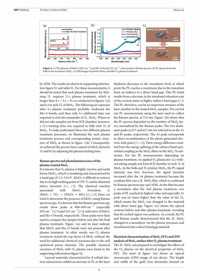
Raman spectra and photoluminescence of theplasma-treatedMoS2It is known that O2 plasma is highly reactive and easilyforms MoO3, which is insulating and characterized bya band gap of 3.2–3.8 eV. MoO3 is difficult to removedue to its highmelting point of 795 °Cand its distortedlattice structure [21, 22]. The chemical reactionassociated with MoO3 formation is
+ +2MoS 7O 2MoO 4SO2 2 3 2 [22–24]. Here, wetried to determine the presence ofMoO3 using Ramanspectroscopy. It is known that theRaman spectroscopyresults show peaks at 800–850 cm−1 (especially820 cm−1) [23] and 225 cm−1 [24], indicative ofMoO3
andMo–O bonds, respectively. These peaks were thenused to compare the samples before and after the finalplasma treatment. Figure 2(a) and its inset indicatethat MoO3 and Mo–O bonds were not present afterplasma treatment. In other words, our O2 plasmatreatment etched the top layers of MoS2 without theneed for additional chemical reactions due to the welloptimized power intensity. The possible chemicalreactions of MoS2 with O2 plasma were listed in thesupporting information figure S2.
Layered materials characterized by d-orbital elec-tron interactions exhibit an increase in PL as the layer
thickness decreases to the monolayer level, at whichpoint the PL reaches a maximum due to the transitionfrom an indirect to a direct band gap. This PL trendresults from a decrease in the intraband relaxation rateof the exciton states at higher indirect band gaps [11].The PL, therefore, can be an important measure of thelayer number in the treated MoS2 samples. We carriedout PL measurements using the laser used to collectthe Raman spectra, at 532 nm. Figure 2(b) shows thatthe PL spectra depended on the number of MoS2 lay-ers, normalized by the Raman peaks. The two domi-nant peaks at 677 and 627 nm are referred to as the A1and B1 peaks, respectively. The A1 peak correspondsto direct recombination of the photo-generated elec-tron–hole pairs [11, 24]. Their energy difference resul-ted from the energy splitting of the valence band spin-orbital coupling in theMoS2 films on the SiO2/Si sub-strates. For the PL measurements depending onplasma treatment, we applied O2 plasma for 12 s with-out taking sample out from ICP chamber to etch 1L ofMoS2. In the bulk and 3L pristine MoS2, the PL signalintensity was low, however, the signal intensityincreased after the 1st plasma treatment because theresultant film was a 2L MoS2 film, which is confirmedby Raman spectroscopy and AFM. As the film becamea monolayer after the 2nd plasma treatment, twopeaks of PL reached its highest value and especially A1peak was six times higher than the value of the 2L,which means the MoS2 was changed to the materialwith direct band gap. Figure 2(c) shows the opticalcontrast before and after plasma treatment, revealingthat the etched region was uniform. As a result, the PLand Raman results demonstrated that the 3L MoS2changed to a monolayer via the plasma processes andtransitioned into a direct band gapmaterial.
Electrical characterization ofMoS2 FETs andXPSanalysis ofMoS2 surface afterO2 plasma treatmentThe 3L MoS2 was prepared to investigate the effects ofthe O2 plasma on the electrical properties of MoS2FET. The inset of figure 3(a) shows an opticalmicroscopic (OM) image of our device. The lengthand width of the gold (Au) electrodes formed on
Figure 2. (a)The absence ofMoO3 (820 cm−1) andMo-Obond (225 cm−1, inset) peaks in Raman spectra. (b)PL spectra from the
bulk to themonolayerMoS2. (c)OM images of pristineMoS2 and afterO2 plasma treatment.
4
2DMater. 3 (2016) 035002 SKim et al
chromium (Cr) were 1.80 and 3.78 μm, respectively.Prior to O2 plasma treatment, the thickness of theMoS2 filmwas confirmed usingAFM.
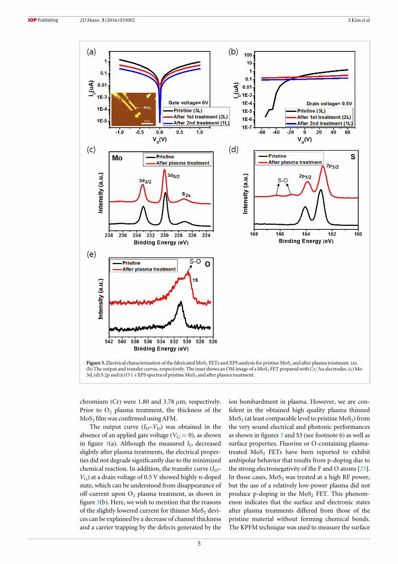
The output curve (ID–VD) was obtained in theabsence of an applied gate voltage (VG = 0), as shownin figure 3(a). Although the measured ID decreasedslightly after plasma treatments, the electrical proper-ties did not degrade significantly due to theminimizedchemical reaction. In addition, the transfer curve (ID–VG) at a drain voltage of 0.5 V showed highly n-dopedstate, which can be understood from disappearance ofoff-current upon O2 plasma treatment, as shown infigure 3(b). Here, we wish to mention that the reasonsof the slightly lowered current for thinner MoS2 devi-ces can be explained by a decrease of channel thicknessand a carrier trapping by the defects generated by the
ion bombardment in plasma. However, we are con-fident in the obtained high quality plasma thinnedMoS2 (at least comparable level to pristineMoS2) fromthe very sound electrical and photonic performancesas shown in figures 3 and S3 (see footnote 6) as well assurface properties. Fluorine or O-containing plasma-treated MoS2 FETs have been reported to exhibitambipolar behavior that results from p-doping due tothe strong electronegativity of the F and O atoms [25].In those cases, MoS2 was treated at a high RF power,but the use of a relatively low-power plasma did notproduce p-doping in the MoS2 FET. This phenom-enon indicates that the surface and electronic statesafter plasma treatments differed from those of thepristine material without forming chemical bonds.The KPFM technique was used to measure the surface
Figure 3.Electrical characterization of the fabricatedMoS2 FETs andXPS analysis for pristineMoS2 and after plasma treatment. (a),(b)The output and transfer curves, respectively. The inset shows anOM image of aMoS2 FET preparedwithCr/Au electrodes. (c)Mo3d, (d) S 2p and (e)O1 sXPS spectra of pristineMoS2 and after plasma treatment.
5
2DMater. 3 (2016) 035002 SKim et al
potential and to investigate the work function altera-tions in later section. These results were intended toelucidate themechanism responsible for then-doping.
The XPS analysis on the pristine and 12 s plasma-treated MoS2 was conducted to determine the surfacechemical compositions. Figures 3(c)–(e) show the XPSresults of Mo, S and O, respectively, for the pristineand plasma treated samples. TheMo 3d peak positionsat binding energies of 229.8 and 232.5 eV and S 2 speak at 227 eV were observed. A peak at 236 eV(Mo+6) indicating the formation of MoO3 was notobserved after the plasma treatment [26]. Two peaks atbinding energies of 162.8 eV and 164.0 eV corresp-onding to S 2p3/2 and 2p1/2, respectively, wereobserved. The interesting change is that other spec-trum was generated at 529.8 eV after plasma treat-ment; it was documented that S–O bond of O 1s [27].It is also supported by an additional doublet peak at∼165 eV as S 2p spectrum, indicating the oxidation ofsulfur [28]. The oxygen atoms seem to substitute forthe etched Mo atoms, resulting in the S–O bonds asdescribed in figure 1(d). In addition, atomic percent-age of S was measured to be 59.5% (Mo: 30.8% and O:9.7%) and it changed to 53.4% (Mo: 31.0% and O:15.6%) after plasma treatment. That is, the ratiobetween Mo and S atom (S/Mo) was 2 for the pristineMoS2; however it changed to 1.7 after plasma treat-ment. The highly n-doped properties shown in ID–VG
after plasma treatment also infer the generation of Svacancies as discussed previously. Hence, it is con-cluded that MoO3 was not formed after plasma treat-ment; however S–O bonds and S vacancies weregenerated from the reaction of oxygen plasma with Satoms and ion bombardment, respectively.
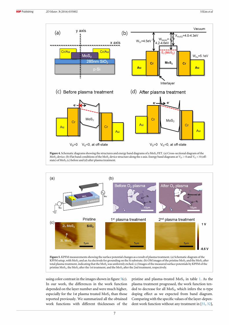
Operatingmechanismunderlying theMoS2 FET,described using band energy diagramsPrior to analyzing the effects of the plasma treatmenton the MoS2 FETs by KPFM, we interpreted theelectron transport using a band energy diagram. Theschematic diagram of our MoS2 device is shown infigure 4(a). The horizontal axis of our MoS2 FETreveals that theMoS2 is contacted with the Cr adhesivelayer underneath the Au layer, and the difference intheir work functions is illustrated in flat band condi-tions, as shown in figure 4(b). The electron affinity forMoS2 is 4.0–4.2 eV, and the work functions of Cr andAu are 4.5 and 5.1 eV, respectively [4]. There have beensome reports on the formation of interlayer such asMo metal or CrSx mixed layers between MoS2 and Cr[29, 30]. Although unintended interlayer could beformed betweenMoS2 and Cr electrodes, ID–VG curveof pristine MoS2 showed a well-known n-type semi-conducting behavior as shown in figure 3(b), indicat-ing that the work function of interlayer is close to theconduction band edge of MoS2 and the influences ofthis interlayer could be negligible. In this regard, we
included interlayer in the band diagram being close tothe conduction band edge ofMoS2.
Figures 4(c) and (d) reveals the band diagrambefore and after plasma treatment with application ofa positive VD and a negative VG. As shown in the ID–VG curve in figure 3(b), the pristine MoS2 showed off-state at negative VG. It seems to be originated from thehigh barrier height between source and drain electro-des, which can disturb the electron flow as described in(c). In contrast, the plasma-treatedMoS2 did not showoff-state, indicating that the highly n-doped stateresulting in the high field emission current despite thenegative VG was applied as described in (d). To corro-borate our band diagram interpretation, we measuredthe changes in surface potential and work functionafter plasma treatment byKPFM.
Surface potential andwork function differences,confirmed byKPFMThe KPFM technique is effective to measure the localcontact potential difference (CPD) between an AFM tipand a sample. Figure 5(a) illustrates the KPFM setupusing aMoS2 sample and a grounded Au electrode. TheCPDbetween the tip and the sample can bedefined as:
D = - ( )e V W W , 1CPD tip sample
whereWtip andWsample are the average work functionsof the tip and the sample (e.g., HOPG or MoS2),respectively, and e is the electronic charge. The surfacepotential was measured by applying an AC voltageamplitude of 2 V and a resonant frequency of 17 kHzto the tip under ambient atmospheric conditions. Thetip was calibrated prior to probing the absolute valuesof the surface potential and the changes in the workfunction of MoS2 upon O2 plasma treatment. Thework function of the tip was obtained using HOPG asawell-definedwork functionmaterial. Prior to collect-ing the measurements, HOPG was annealed(WHOPG= 4.6 eV) at 250 °C for 3 h under the forminggas (Ar/H2) to remove the effects of humidity. The tipcalibration with HOPG yielded a work function of4.91 eV for the Au-coated tip. This tip work functionwas used to measure the surface potential of pristineMoS2 in the tri-layer and bi-layer forms after O2
plasma treatment. The OM images in figure 5(b) showthe pristine film and the film after complete plasmatreatment, indicating that the etching process was welldefined. The CPD values of the 3L pristine MoS2,MoS2 after the 1st treatment and 2nd treatment were –0.294 eV, 0.001 eV and 0.078 eV, respectively, whereasthe CPD value of the 2L pristine MoS2 and MoS2 afterthe 1st treatment were −0.192 eV and 0.108 eV,respectively. The absolute values of the MoS2 workfunction could be estimated as:
D = -( ) ( )e V W W4.91 eV . 2CPD tip MoS2
The work function of the 3L pristine MoS2decreased from 5.20 eV to 4.91 eV for 2L and 4.83 eVfor 1L, and that for the 2L pristine film decreased from5.10 eV to 4.80 eV. These changes are highlighted
6
2DMater. 3 (2016) 035002 SKim et al
using color contrast in the images shown in figure 5(c).In our work, the differences in the work functiondepended on the layer number and weremuch higher,especially for the 1st plasma treated MoS2 than thosereported previously. We summarized all the obtainedwork functions with different thicknesses of the
pristine and plasma-treated MoS2 in table 1. As theplasma treatment progressed, the work function ten-ded to decrease for all MoS2, which infers the n-typedoping effect as we expected from band diagram.Comparing with the specific values of the layer-depen-dent work function without any treatment in [31, 32],
Figure 4. Schematic diagrams showing the structures and energy band diagrams of aMoS2 FET. (a)Cross-sectional diagramof theMoS2 device. (b) Flat band conditions of theMoS2 device structure along the x axis. Energy band diagrams atVD> 0 andVG< 0 (off-state) ofMoS2 (c) before and (d) after plasma treatment.
Figure 5.KPFMmeasurements showing the surface potential changes as a result of plasma treatment. (a) Schematic diagramof theKPFM setup, withMoS2 and anAu electrode for grounding on the Si substrate. (b)OM images of the pristineMoS2 and theMoS2 aftertotal plasma treatment, indicating that theMoS2was uniformly etched. (c) Images of themeasured surface potentials byKPFMof thepristineMoS2, theMoS2 after the 1st treatment, and theMoS2 after the 2nd treatment, respectively.
7
2DMater. 3 (2016) 035002 SKim et al
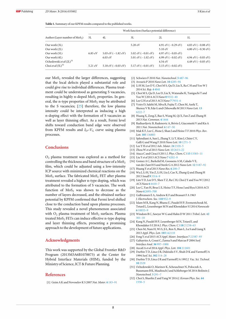
our MoS2 revealed the larger differences, suggestingthat the local defects played a substantial role andcould give rise to individual differences. Plasma treat-ment could be understood as generating S vacancies,resulting in highly n-doped MoS2 properties. In gen-eral, the n-type properties of MoS2 may be attributedto the S vacancies; [25] therefore, the low plasmaintensity could be interpreted as inducing a highn-doping effect with the formation of S vacancies aswell as layer thinning effect. As a result, Fermi levelshifts toward conduction band edge were observedfrom KPFM results and ID–VG curve using plasmaprocesses.
Conclusions
O2 plasma treatment was explored as a method forcontrolling the thickness and band structure of aMoS2film, which could be adjusted using a low-intensityICP source with minimized chemical reactions on theMoS2 surface. The fabricated MoS2 FET after plasmatreatment revealed a higher n-type doping, which wasattributed to the formation of S vacancies. The workfunction of MoS2 was shown to decrease as thenumber of layers decreased, and the obtained surfacepotential by KPFM confirmed that Fermi level shiftedclose to the conduction band upon plasma processes.This study revealed a novel phenomenon associatedwith O2 plasma treatment of MoS2 surfaces. Plasmatreated MoS2 FETs can induce effective n-type dopingand layer thinning effects, presenting a promisingapproach to the development of future applications.
Acknowledgments
This work was supported by the Global Frontier R&DProgram (2013M3A6B1078873) at the Center forHybrid Interface Materials (HIM), funded by theMinistry of Science, ICT&Future Planning.
References
[1] GeimAK andNovoselovK S 2007Nat.Mater. 6 183–91
[2] Schwierz F 2010Nat. Nanotechnol. 5 487–96[3] Avouris P 2010Nano Lett. 10 4285–94[4] LiHM, LeeDY, ChoiMS,QuD, LiuX, RaCHandYooW J
2014 Sci. Rep. 4 4041[5] ChoiMS,QuD, LeeD, LiuX,WatanabeK, Taniguchi T and
YooW J 2014ACSNano 8 9332–40[6] LeeGH et al 2013ACSNano 7 7931–6[7] VoiryD, SalehiM, Silva R, Fujita T, ChenM,Asefa T,
ShenoyVB, EdaG andChhowallaM2013Nano Lett. 136222–7
[8] HuangX, Zeng Z, Bao S,WangM,QiX, FanZ andZhangH2013Nat. Commun. 4 1444
[9] Radisavljevic B, Radenovic A, Brivio J, Giacometti V andKis A2011Nat. Nanotechnol. 6 147–50
[10] MakKF, Lee C,Hone J, Shan J andHeinz T F 2010Phys. Rev.Lett. 105 136805
[11] Splendiani A, Sun L, Zhang Y, Li T, Kim J, ChimCY,Galli G andWang F 2010Nano Lett. 10 1271–5
[12] Lee YH et al 2012Adv.Mater. 24 2320–5[13] ZhouW et al 2013Nano Lett. 13 2615–22[14] AtacaC andCiraci S 2011 J. Phys. Chem.C 115 13303–11[15] Liu Y et al 2013ACSNano 7 4202–9[16] GomezAC, BarkelidM,Goossens AM,CaladoVE,
van der ZantH S and Steele GA2012Nano Lett. 12 3187–92[17] HuangY et al 2013NanoRes. 6 200–7[18] Wu J, LiH, YinZ, LiH, Liu J, CaoX, ZhangQ andZhangH
2013 Small 9 3314–9[19] LimYD, LeeDY, ShenTZ, RaCH,Choi J Y andYooW J 2012
ACSNano 6 4410–7[20] LeeC, YanH, Brus L E,Heinz T F,Hone J andRyu S 2010ACS
Nano 4 2695–700[21] Gulbransen EA, AndrewKF andBrassart FA 1963
J. Electrochem. Soc. 110 952–9[22] IslamMR,KangN, BhanuU, PaudelHP, ErementchoukM,
Tetard L, LeuenbergerMNandKhondaker S I 2014Nanoscale6 10033–9
[23] WindomBC, SawyerWGandHahnDW2011Tribol. Lett. 42301–10
[24] KangN, PaudelHP, LeuenbergerMN,Tetard L andKhondaker S I 2014 J. Phys. Chem.C 118 21258–63
[25] ChenM,NamH,Wi S, Ji L, RenX, Bian L, Lu S and LiangX2013Appl. Phys. Lett. 103 142110
[26] Feng Y et al 2015ACSAppl.Mater. Interfaces 7 22587–93[27] Galtayries A, Cousi C, Zanna S andMarcus P 2004 Surf.
Interface Anal. 36 997–1000[28] Azcatl A et al 2014Appl. Phys. Lett. 104 111601[29] Durbin TD, Lince J R,Didziulis SV, ShuhDK andYarmoff J A
1994 Surf. Sci. 302 314–28[30] Durbin TD, Lince J R andYarmoff J A 1992 J. Vac. Sci. Technol.
10 2529[31] OchedowskiO,MarinovK, ScheuschnerN, Poloczek A,
BussmannBK,Maultzsch J and SchlebergerM2014Beilstein J.Nanotechnol. 5 291–7
[32] Choi S, Shaolin Z andYangW2014 J. Korean Phys. Soc. 641550–5
Table 1. Summary of ourKPFM results compared to the publishedworks.
Work function (Surface potential difference)
Author (Layer number ofMoS2) 5L 4L 3L 2L 1L
Ourwork (3L) 5.20 eV 4.91 eV (−0.29 eV) 4.83 eV (−0.08 eV)Ourwork (2L) 5.10 eV 4.80 eV (−0.30 eV)Ourwork (5L) 6.85 eV 5.03 eV (−1.82 eV) 5.02 eV (−0.01 eV) 4.97 eV (−0.05 eV)Ourwork (4L) 6.03 eV 5.01 eV (−1.02 eV) 4.99 eV (−0.02 eV) 4.94 eV (−0.05 eV)Ochedowski et al (2L)31 4.54 eV 4.49 eV (−0.05 eV)Choi et al (5L)32 5.21 eV 5.18 eV (−0.03 eV) 5.17 eV (−0.01 eV) 5.15 eV (−0.02 eV)
8
2DMater. 3 (2016) 035002 SKim et al
Related Documents