HAL Id: hal-03260241 https://hal.archives-ouvertes.fr/hal-03260241 Submitted on 14 Oct 2021 HAL is a multi-disciplinary open access archive for the deposit and dissemination of sci- entific research documents, whether they are pub- lished or not. The documents may come from teaching and research institutions in France or abroad, or from public or private research centers. L’archive ouverte pluridisciplinaire HAL, est destinée au dépôt et à la diffusion de documents scientifiques de niveau recherche, publiés ou non, émanant des établissements d’enseignement et de recherche français ou étrangers, des laboratoires publics ou privés. Effects of Creep Failure Mechanisms on Thermomechanical Reliability of Solder Joints in Power Semiconductors Vahid Samavatian, Hossein Iman-Eini, yvan Avenas, Majid Samavatian To cite this version: Vahid Samavatian, Hossein Iman-Eini, yvan Avenas, Majid Samavatian. Effects of Creep Failure Mech- anisms on Thermomechanical Reliability of Solder Joints in Power Semiconductors. IEEE Transactions on Power Electronics, Institute of Electrical and Electronics Engineers, 2020, 35 (9), pp.8956–8964. 10.1109/TPEL.2020.2973312. hal-03260241

Welcome message from author
This document is posted to help you gain knowledge. Please leave a comment to let me know what you think about it! Share it to your friends and learn new things together.
Transcript
HAL Id: hal-03260241https://hal.archives-ouvertes.fr/hal-03260241
Submitted on 14 Oct 2021
HAL is a multi-disciplinary open accessarchive for the deposit and dissemination of sci-entific research documents, whether they are pub-lished or not. The documents may come fromteaching and research institutions in France orabroad, or from public or private research centers.
L’archive ouverte pluridisciplinaire HAL, estdestinée au dépôt et à la diffusion de documentsscientifiques de niveau recherche, publiés ou non,émanant des établissements d’enseignement et derecherche français ou étrangers, des laboratoirespublics ou privés.
Effects of Creep Failure Mechanisms onThermomechanical Reliability of Solder Joints in Power
SemiconductorsVahid Samavatian, Hossein Iman-Eini, yvan Avenas, Majid Samavatian
To cite this version:Vahid Samavatian, Hossein Iman-Eini, yvan Avenas, Majid Samavatian. Effects of Creep Failure Mech-anisms on Thermomechanical Reliability of Solder Joints in Power Semiconductors. IEEE Transactionson Power Electronics, Institute of Electrical and Electronics Engineers, 2020, 35 (9), pp.8956–8964.�10.1109/TPEL.2020.2973312�. �hal-03260241�
Abstract— This paper deals with the effects of creep failure
mechanism on thermo-mechanical reliability of power
semiconductors. Regarding power semiconductors’ working
conditions, fatigue and creep failure mechanisms are the two most
critical failure origins in power semiconductors. Here we propose
an approach to show the role of creep event on the creep-fatigue
failure mechanism of a power semiconductor. The results show
that 34% difference in the lifetime prediction appears when the
creep is considered in the estimations. This indicates that the extra
effect of creep on fatigue evolution of power systems can markedly
decrease the lifetime which is ignored in many cases. Moreover, a
logarithmic trend for thermal resistance and on state voltage drop
upon increase in number of thermo-mechanical cycles implies the
accelerated aging of power semiconductor.
Index Terms— physics of failure, reliability assessment, creep,
fatigue, Power semiconductor, thermo-mechanical reliability.
I. INTRODUCTION
NE of the most vulnerable part in power converters is
undoubtedly power semiconductor [1], [2]. Power devices
play central roles in the performances of power converters.
These devices are strictly exposed to internal and external
stresses. Regarding their laminated structures, the most
important stressor, they are exposed to, is electro thermo-
mechanical stress [3]. Although, considerable studies have
taken into account electro thermo-mechanical fatigue failure
mechanisms [4], [5], another important failure mechanism,
namely creep mechanism, has been neglected.
Many studies have been done to evaluate the effects of
thermo-mechanical cycling on the reliability of solder joints in
electronic packages. Amalu et al [6] investigated the thermo-
mechanical response of solder joints in a crystalline silicon
solar cell assembly using Garofalo-Arrhenius creep model.
Their results indicate that the joint dimension plays a vital role
in the thermo-mechanical reliability of solder joints.
Talebanpour et al [7] investigated the influence of thermal-
mechanical history on the creep behavior of Sn-based solders.
It was found that during power cycles ranging from 0.44 to 0.8
Tmax, the thermal cycling reliability of power electronic
packages was steeply declined. Le et al [8] indicated that
process-induced voids acts as a key role in the creep-fatigue
lifetime of solder joints of a power module. The voids are the
potential sites for the concentration of stress and crack initiation
V. Samavatian is with the School of Electrical and Computer Engineering, College of
Engineering, University of Tehran, Tehran, Iran and the Univ. Grenoble Alpes, CNRS,
Grenoble INP (Institute of Engineering Univ. Grenoble Alpes), G2Elab, 38000 Grenoble,
France (e-mail: [email protected]).
H. Iman-Eini is with the School of Electrical and Computer Engineering, College of
Engineering, University of Tehran, Tehran, Iran (e-mail: [email protected]).
in the solder joints. There are also some other works modeling
and demonstrating the role of primary voids trapped in the
solder material [9], [10]. Zhang et al [11] used finite element
simulation and showed that the maximum stress concentrated
location established a relationship with heights of solder joints.
Chen et al [12] proposed a model to evaluate the coupling
damage effects of low cycle fatigue and creep events under
thermal cycling of an electronic device. Their case study on a
lead free solder joint validated the damage model. Coffin-
Manson method was used to evaluate the solder joints in a
package-on-package structure [13]. It was reported that the
maximum inelastic hysteresis energy accumulates on the solder
joints in the bottom fine-pitch ball grid array structure. The
thermal-fatigue crack also initiates in the two symmetrical
corners of solder balls in fine-pitch ball grid array structure.
Zhang et al [14] applied simulation along with Taguchi method
to study the thermo-mechanical reliability of solder joints in a
FGBGA device subjected to a thermal cyclic loading. They
revealed that the solder material is the most significant factor
among the control factors in the device. Baber and Guven [15]
proposed a peridynamic approach to predict fatigue lifetime of
solder joints. This approach expresses that the material
degradation through energy dissipative mechanisms plays a key
role in crack initiation and propagation and the cracks follow
paths similar to cracks produced under quasi-static cycling.
Metais et al [16] proposed a viscoplastic-fatigue-creep damage
model based on a non-linear mechanical behavior of solder at
the beginning of deformation as well as during continuous
cyclic aging. Material modeling concentrated on the
interpretation of the complicated interaction between fatigue
and creep and viscoplastic processes. Their results had a good
agreement with the experimental works.
Regarding the conditions under which power devices are
working, creep as well as fatigue failure mechanisms both may
be activated. Consideration of creep effects along with fatigue
failure mechanism is still under debate in the power electronics
field. The objective of this paper is to address the raised
question that how the interaction of fatigue and creep failure
mechanisms influences the damage evolution of solder joints in
power devices in real conditions. Therefore, this paper is
prepared to carry out the real mission profile based coupled
creep-fatigue useful lifetime estimation. Using FEM
simulation, basic data associated to the steady state creep strain
rate is provided. The data is utilized to evaluate damage
Y. Avenas is with the Univ. Grenoble Alpes, CNRS, Grenoble INP (Institute of
Engineering Univ. Grenoble Alpes), G2Elab, 38000 Grenoble, France (e-mail:
M. Samavatian is with the Department of Advanced Materials and Renewable Energy,
Iranian Research Organization for Science and Technology (IROST), Tehran, Iran (email:
Vahid Samavatian, Hossein Iman-Eini, Senior Member, IEEE, Yvan Avenas and Majid Samavatian
Effects of Creep Failure Mechanisms on Thermo-
mechanical Reliability of Solder Joints in Power
Semiconductors
O
evolution with the coupled damage approach. Furthermore,
experimental tests are used to deeply study the actual aspect of
this failure mechanism in the solder joint. The remainder of this
paper is organized as follows: Section II deals with the probable
failure mechanisms in the power semiconductors. While section
III deals with the proposed creep-fatigue reliability framework,
experimental procedure and finite element (FE) simulation are
respectively discussed in sections IV and V. Results and
discussion are carried out in section VI.
II. CRITICAL FAILURE MECHANISMS
A. Electro-thermo-mechanical fatigue failure mechanism
From a physical point of view, the repeated variations of
stress may induce alternate plastic strains producing internal
micro stresses responsible of microdecohesions by slip band
arrests. The initiated micro cracks grow either inside the
crystals or along the grains boundaries, depending on the
materials and the loadings, up to coalescence corresponding to
initiation of a mesocrack. Plastic strain and stress both
participate in this phenomenon [17].
Power semiconductors are exposed to different thermal
cycles owing to their power losses made in the chip junction.
Electrical losses lead to heating up the bodies and consequently
these temperature changes cause thermal strains. Regarding
physical structure of power devices comprising various layers
with different coefficients of thermal expansion (CTE) from
3.5×10⁻⁶/K for silicon to 17×10-6/K for copper and 22.3×10⁻⁶/K
for aluminum, a meaningful set of shear and normal stresses are
induced in these layers [4]. These thermal stresses finally lead
to the thermal strains in all bodies. Thereby, electro-thermo-
mechanical fatigue has been occurred during the power
semiconductor operations and may influence the health of
power devices. The fatigue phenomenon leads to micro cracks
production and growth as well as voids creation and
coalescence which can affect the performance of any parts of
packaging in a power device comprising bonding wires,
aluminum metallization, die attach to the baseplate, etc.
B. Solder joint creep-fatigue failure mechanism
In general, the time-dependent strength of most materials
deteriorates with the increase in the operating temperature. The
creep and creep-fatigue failures are the events activated with
the rise in temperature above the one-third of melting point of
metals. The mentioned events are intensified upon passing of
the time under external forces acting, when high temperature
induces viscous effects to the materials. Creep-fatigue failures
are the consequence of plastic strains occurring under constant
temperature loading and temperature ramp up/down which
materially solder joint does not differentiate between these two
situations, but possible to be distinguished quantitatively in the
equations. From a physical viewpoint, the evolution of creep
damage includes the formation and growth of micro-voids,
micro-crack formation at inter-granular sites and their
coalescence in the crystals triple points. It is also suggested that
the formation of inter-granular micro-cracks under fatigue
cycles can develop among the grain boundaries and interact
with the defects caused by the creep event. This interaction is
nonlinear and the effects of the accumulated damage are
associated with the materials properties, environmental
conditions, system design and etc. [18], [19].
Regarding low melting temperature, the solder joint is
undoubtedly the most fragile part in the power semiconductor,
as a creep-fatigue failure mechanism point of view. In recent
years, Sn-Ag-Cu (SAC) based solder materials with low
melting point and superior mechanical properties have been
proposed in the electronic industries. However, their reliability
features, including fatigue resistance and creep behavior, play a
major role in power electronic packages. In the meantime, it
was found that solder joints were the most vulnerable parts for
the damage initiation and the failure [20], [21]. In order to
evaluate the reliability of solder joints under a thermo-
mechanical loading, it is required to analyze the creep behavior
of the solder and then the produced strain takes into account of
fatigue evolution.
Recently, several studies have been published on the
constitutive equation for creep strain analysis of SAC solders
[22], [23]. Among them, Garofalo-Arrhenius creep model is
one of the most applicative constitutive models for evaluation
of SAC solder joints [23]. This model proposes a hyperbolic
sine creep equation to model the creep event of the solder joints.
The following equation demonstrates the steady state creep
strain rate [24]:
( ) ( )3C
cr 1 2 4C sinh C exp C T = − (1)
έcr is the creep strain rate and C1, C2, C3 and C4 are constant
values for SAC solder [25]. The creep event is the primary
damage mechanism for Sn-based solder joints under thermal
cycling [24]. Hence, it is necessary to consider the creep strain
in the life prediction model. σ is the applied stresses induced by
temperature swing (ΔT) and thereby they can replace.
C. Lifetime model
C.1. Fatigue failure mechanism lifetime model
On the contrary to passive thermal cycling test in which
temperature swing is being induced by external homogeneous
heating source, the device under test (DUT) is exposed to
electrical loading in active thermal cycling test leading to faster
temperature swing in the DUT junction. The heating up and
cooling down rates generally take a few seconds. These steeply
changes in the junction temperature can make sharp thermo-
mechanical stresses in all bodies. However, in the passive
temperature cycling, all bodies of component are exposed to the
external temperature variations. It takes much higher time in
comparison to active temperature cycles. There are numerous
proposed lifetime estimation models for thermal fatigue failure
mechanism in the active thermal cycling test [26]. Based on
LESIT [27] experiment, the junction temperature swing (∆Tj)
and the mean junction temperature (Tmean) are found to be the
two most important factors in lifetime and damage evolution
models. In addition to these two factors, however, Bayerer et al
[28] have proposed a lifetime model considering on time of the
active cycle (ton) and current per wire bond (I) for the specified
and fixed power semiconductors. Since stationary creep
phenomenon is also involved in this study, Coffin-Manson-
Arrhenius lifetime model has been employed [27]. The model
defined as follows:
f mean j j mN (T , T ) A T exp(Q RT ) = (2)
where A, α are both constant and device-dependent. ΔTj
expresses the junction temperature swing of devices in oC. Nf is
the number of cycle to failure based on the failure criteria
definition. R and Q are the gas constant (8.314 J.Mol-1.K-1),
internal energy and Tmean is the mean junction temperature of
devices in Kelvin.
C.2. Creep lifetime model
In most materials, a temperature increase leads to a decrease
in the strength of material. In the creep mechanism the time and
the temperature are both paramount of importance due to its
physical mechanism. On the contrary to the fatigue damage
process, namely load cycles, creep degradation is time-
dependent and highly impressed by the dwelling time period
[10]. It is worth-mentioning that the pure creep strain is
accumulated during the hot dwelling time, while the induced
strain during the temperature ramping is mainly, not
thoroughly, due to the sharp differences in the CTE of
components and is associated to the fatigue mechanism [12].
For expressing lifetime model of the materials on the creep
failure mechanism, Monkman-Grant (MG) model has been
extensively used [29]:
cr c MGt C = (3)
where έcr is the stable creep strain rate expressed by (1), CMG
and β are constant and material-dependent. It should be noted
that the creep strain in (3) is related to the hot dwelling time.
It was previously mentioned and also revealed from (3) that
the creep failure mechanism is time dependent which means
that the longer time the material is exposed to the roughly
constant temperature, the more degradation occurs. Based on
Monkman-Grant model, the dwelling time (Δt) is a key factor
in calculating the creep useful lifetime.
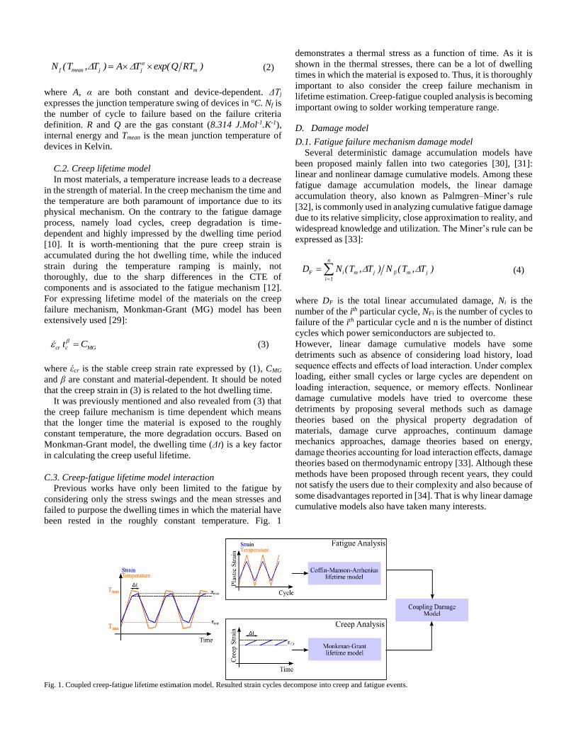
C.3. Creep-fatigue lifetime model interaction
Previous works have only been limited to the fatigue by
considering only the stress swings and the mean stresses and
failed to purpose the dwelling times in which the material have
been rested in the roughly constant temperature. Fig. 1
demonstrates a thermal stress as a function of time. As it is
shown in the thermal stresses, there can be a lot of dwelling
times in which the material is exposed to. Thus, it is thoroughly
important to also consider the creep failure mechanism in
lifetime estimation. Creep-fatigue coupled analysis is becoming
important owing to solder working temperature range.
D. Damage model
D.1. Fatigue failure mechanism damage model
Several deterministic damage accumulation models have
been proposed mainly fallen into two categories [30], [31]:
linear and nonlinear damage cumulative models. Among these
fatigue damage accumulation models, the linear damage
accumulation theory, also known as Palmgren–Miner’s rule
[32], is commonly used in analyzing cumulative fatigue damage
due to its relative simplicity, close approximation to reality, and
widespread knowledge and utilization. The Miner’s rule can be
expressed as [33]:
n
F i m j fi m j
i 1
D N (T , T ) N (T , T ) =
= (4)
where DF is the total linear accumulated damage, Ni is the
number of the ith particular cycle, NFi is the number of cycles to
failure of the ith particular cycle and n is the number of distinct
cycles which power semiconductors are subjected to.
However, linear damage cumulative models have some
detriments such as absence of considering load history, load
sequence effects and effects of load interaction. Under complex
loading, either small cycles or large cycles are dependent on
loading interaction, sequence, or memory effects. Nonlinear
damage cumulative models have tried to overcome these
detriments by proposing several methods such as damage
theories based on the physical property degradation of
materials, damage curve approaches, continuum damage
mechanics approaches, damage theories based on energy,
damage theories accounting for load interaction effects, damage
theories based on thermodynamic entropy [33]. Although these
methods have been proposed through recent years, they could
not satisfy the users due to their complexity and also because of
some disadvantages reported in [34]. That is why linear damage
cumulative models also have taken many interests.
Fig. 1. Coupled creep-fatigue lifetime estimation model. Resulted strain cycles decompose into creep and fatigue events.
D.2. Creep damage model
There are many damage models available for solder creep.
They can be categorized into three groups: creep strain based,
creep energy based, and damage accumulation based [25].
Damage accumulation model is based on the MG model. Thus,
one can find time per unit creep damage as follows:
( )1
C c MGd 1 t C
= = (5)
Accumulated creep damage during the dwelling period under
the same condition gives as
( )1
C c MGD t t t C
= = (6)
where Δt is the dwelling time. Creep damage accumulation
model has been widely used in several studies and can predict
the useful lifetime with an acceptable precision [35].
D.3. Coupled creep-fatigue damage model
Although there are many fatigue-creep damage coupling
models such as strain range partitioning, strain energy
partitioning, frequency-modified strain-life equation, unified
damage and mechanism-based model [36], [37], the global
linear damage model [37] will be assumed and expressed as
follows
F CD D D= + (7)
where DF and DC are defined by (4) and (6) respectively.
III. CREEP-FATIGUE RELIABILITY FRAMEWORK
In this section, the effects of creep failure mechanism
consideration in the reliability assessment of power electronic
semiconductors will be discussed. In this case, for the lifetime
models of power devices both Coffin-Manson-Arrhenius (2)
and Monkman-Grant (3) have been employed for fatigue and
creep failure mechanisms, respectively. Global linear damage
model (7) has been also used for obtaining accumulated damage
in the power semiconductors.
The procedure of the proposed framework for useful lifetime
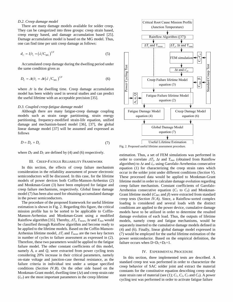
estimation is shown in Fig. 2. Regarding this figure, the critical
mission profile has to be sorted to be applicable to Coffin-
Manson-Arrhenius and Monkman-Grant using a modified
Rainflow algorithm [35]. Thereby, ΔTj, Tmean, ∆t and Tmax would
be classified through Rainflow algorithm and become ready to
be applied to the lifetime models. Based on the Coffin-Manson-
Arrhenius lifetime model, ΔTj and Tmean are the two key factors
in number of cycles to failure assessment as expressed in (2).
Therefore, these two parameters would be applied to the fatigue
failure model. The other constant coefficients of this model,
namely A, α and Q, were extracted from power cycling tests
considering 20% increase in their critical parameters, namely
on-state voltage and junction-case thermal resistance, as the
failure criteria in individual test under a unique specified
conditions (Section IV.B). On the other side based on the
Monkman-Grant model, dwelling time (∆t) and creep strain rate
(έcr) are the most important parameters in the creep lifetime
Fig. 2. Proposed useful lifetime assessment procedure.
estimation. Thus, a set of FEM simulations was performed in
order to correlate ΔTj, ∆t and Tmax (obtained from Rainflow
algorithm) to ∆t and έcr using Garofalo-Arrehenius consecutive
equation (1) for characterizing the creep strain rates which
occur in the solder joint under different conditions (Section V).
These processed data would be applied to Monkman-Grant
lifetime model in order to calculate damage evolution regarding
creep failure mechanism. Constant coefficients of Garofalo-
Arrehenius consecutive equation (C1 to C4) and Monkman-
Grant lifetime model (CMG and β) were extracted from standard
creep tests (Section IV.A). Since, a Rainflow-sorted complex
loading is considered and several loads with the distinct
conditions are applied to the power device, cumulative damage
models have to be utilized in order to determine the resulted
damage evolution of each load. Thus, the outputs of lifetime
models, namely creep and fatigue mechanisms, would be
separately inserted to the cumulative damage models defined in
(4) and (6). Finally, linear global damage model expressed in
(7) would be employed for the useful lifetime estimation of the
power semiconductor. Based on the empirical definition, the
failure occurs when D=DC+DF=1.
IV. EXPERIMENTAL PROCEDURE
In this section, three implemented tests are described. A
standard creep test was performed in order to characterize the
creep behavior of SAC solder joint and extract the material
constants for the constitutive equation describing creep steady
state strain rate of material (see (1); C1, C2, C3 and C4). A power
cycling test was performed in order to activate fatigue failure
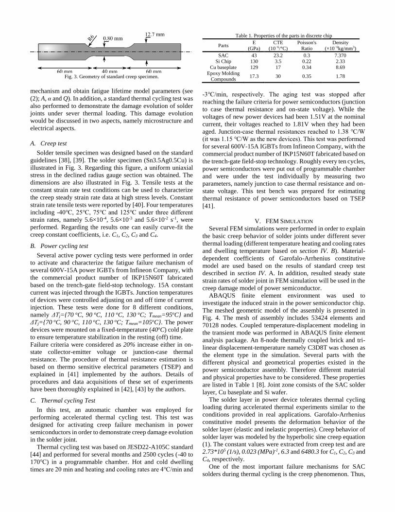
Fig. 3. Geometry of standard creep specimen.
mechanism and obtain fatigue lifetime model parameters (see
(2); A, α and Q). In addition, a standard thermal cycling test was
also performed to demonstrate the damage evolution of solder
joints under sever thermal loading. This damage evolution
would be discussed in two aspects, namely microstructure and
electrical aspects.
A. Creep test
Solder tensile specimen was designed based on the standard
guidelines [38], [39]. The solder specimen (Sn3.5Ag0.5Cu) is
illustrated in Fig. 3. Regarding this figure, a uniform uniaxial
stress in the declined radius gauge section was obtained. The
dimensions are also illustrated in Fig. 3. Tensile tests at the
constant strain rate test conditions can be used to characterize
the creep steady strain rate data at high stress levels. Constant
strain rate tensile tests were reported by [40]. Four temperatures
including -40℃, 25℃, 75℃ and 125℃ under three different
strain rates, namely 5.6×10⁻⁴, 5.6×10⁻³ and 5.6×10⁻² s-1, were
performed. Regarding the results one can easily curve-fit the
creep constant coefficients, i.e. C1, C2, C3 and C4.
B. Power cycling test
Several active power cycling tests were performed in order
to activate and characterize the fatigue failure mechanism of
several 600V-15A power IGBTs from Infineon Company, with
the commercial product number of IKP15N60T fabricated
based on the trench-gate field-stop technology. 15A constant
current was injected through the IGBTs. Junction temperatures
of devices were controlled adjusting on and off time of current
injection. These tests were done for 8 different conditions,
namely ΔTj={70 oC, 90 oC, 110 oC, 130 oC; Tmean=95oC} and
ΔTj={70 oC, 90 oC, 110 oC, 130 oC; Tmean=105oC}. The power
devices were mounted on a fixed-temperature (40oC) cold plate
to ensure temperature stabilization in the resting (off) time.
Failure criteria were considered as 20% increase either in on-
state collector-emitter voltage or junction-case thermal
resistance. The procedure of thermal resistance estimation is
based on thermo sensitive electrical parameters (TSEP) and
explained in [41] implemented by the authors. Details of
procedures and data acquisitions of these set of experiments
have been thoroughly explained in [42], [43] by the authors.
C. Thermal cycling Test
In this test, an automatic chamber was employed for
performing accelerated thermal cycling test. This test was
designed for activating creep failure mechanism in power
semiconductors in order to demonstrate creep damage evolution
in the solder joint.
Thermal cycling test was based on JESD22-A105C standard
[44] and performed for several months and 2500 cycles (-40 to
170℃) in a programmable chamber. Hot and cold dwelling
times are 20 min and heating and cooling rates are 4℃/min and
Table 1. Properties of the parts in discrete chip
Parts E
(GPa) CTE
(10−6/°C) Poisson's
Ratio Density
(×10−6kg/mm3)
SAC 43 23.2 0.3 7.370 Si Chip 130 3.5 0.22 2.33
Cu baseplate 129 17 0.34 8.69
Epoxy Molding Compounds
17.3 30 0.35 1.78
-3℃/min, respectively. The aging test was stopped after
reaching the failure criteria for power semiconductors (junction
to case thermal resistance and on-state voltage). While the
voltages of new power devices had been 1.51V at the nominal
current, their voltages reached to 1.81V when they had been
aged. Junction-case thermal resistances reached to 1.38 ℃/W
(it was 1.15 ℃/W as the new devices). This test was performed
for several 600V-15A IGBTs from Infineon Company, with the
commercial product number of IKP15N60T fabricated based on
the trench-gate field-stop technology. Roughly every ten cycles,
power semiconductors were put out of programmable chamber
and were under the test individually by measuring two
parameters, namely junction to case thermal resistance and on-
state voltage. This test bench was prepared for estimating
thermal resistance of power semiconductors based on TSEP
[41].
V. FEM SIMULATION
Several FEM simulations were performed in order to explain
the basic creep behavior of solder joints under different sever
thermal loading (different temperature heating and cooling rates
and dwelling temperature based on section IV. B). Material-
dependent coefficients of Garofalo-Arrhenius constitutive
model are used based on the results of standard creep test
described in section IV. A. In addition, resulted steady state
strain rates of solder joint in FEM simulation will be used in the
creep damage model of power semiconductor.
ABAQUS finite element environment was used to
investigate the induced strain in the power semiconductor chip.
The meshed geometric model of the assembly is presented in
Fig. 4. The mesh of assembly includes 53424 elements and
70128 nodes. Coupled temperature-displacement modeling in
the transient mode was performed in ABAQUS finite element
analysis package. An 8-node thermally coupled brick and tri-
linear displacement-temperature namely C3D8T was chosen as
the element type in the simulation. Several parts with the
different physical and geometrical properties existed in the
power semiconductor assembly. Therefore different material
and physical properties have to be considered. These properties
are listed in Table 1 [8]. Joint zone consists of the SAC solder
layer, Cu baseplate and Si wafer.
The solder layer in power device tolerates thermal cycling
loading during accelerated thermal experiments similar to the
conditions provided in real applications. Garofalo-Arrhenius
constitutive model presents the deformation behavior of the
solder layer (elastic and inelastic properties). Creep behavior of
solder layer was modeled by the hyperbolic sine creep equation
(1). The constant values were extracted from creep test and are
2.73*105 (1/s), 0.023 (MPa)-1, 6.3 and 6480.3 for C1, C2, C3 and
C4, respectively.
One of the most important failure mechanisms for SAC
solders during thermal cycling is the creep phenomenon. Thus,
creep induced deformation can affect the lifetime of solder layer
and propagate the cracks and the voids. Creep strain rate can be
extracted using FEM simulation. The average values of creep
strain rate in a solder joint was used to estimate the cumulative
creep damage process.
VI. RESULTS AND DISCUSSION
In this section, in order to describe the evolution of creep-
fatigue event in the solder joint under thermal loading, some
basic FEM results are explained in details. In addition, the
damage evolution of thermal loading on the solder joint is also
explained based on the experimental tests to demonstrate the
actual effects of creep-fatigue damage in solder joints.
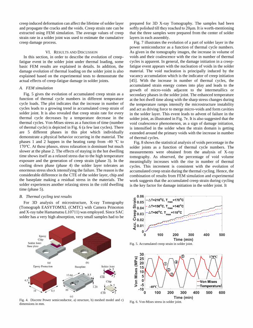
A. FEM simulation
Fig. 5 gives the evolution of accumulated creep strain as a
function of thermal cycle numbers in different temperature
cycle loads. The plot indicates that the increase in number of
cycles leads to a growing trend in accumulated creep strain of
solder joint. It is also revealed that creep strain rate for every
thermal cycle decreases by a temperature decrease in the
thermal cycles. Von-Mises stress as a function of time (number
of thermal cycle) is depicted in Fig. 6 (a few last cycles). There
are 5 different phases in this plot which individually
demonstrate a physical behavior occurring in the material. The
phases 1 and 2 happen in the heating ramp from -40 ℃ to
170℃. At these phases, stress relaxation is dominant but much
slower at the phase 2. The effects of staying in the hot dwelling
time shows itself as a relaxed stress due to the high temperature
exposure and the generation of creep strain (phase 3). In the
cooling down phase (phase 4) the solder layer tolerates an
enormous stress shock intensifying the failure. The reason is the
considerable difference in the CTE of the solder layer, chip and
the baseplate making a residual stress in the materials. The
solder experiences another relaxing stress in the cold dwelling
time (phase 5).
B. Thermal cycling test results
For 3D analysis of microstructure, X-ray Tomography
(Tomograph EASYTOMXL (CMTC) with Camera Princeton
and X-ray tube Hamamatsu L10711) was employed. Since SAC
solder has a very high absorption, very small samples had to be
Fig. 4. Discrete Power semiconductor, a) structure, b) meshed model and c)
dimensions in mm.
prepared for 3D X-ray Tomography. The samples had been
softly polished till they reached to 20μm. It is worth-mentioning
that the three samples were prepared from the center of solder
layers in each assembly.
Fig. 7 illustrates the evolution of a part of solder layer in the
power semiconductor as a function of thermal cycle numbers.
As given in the tomography images, the increase in volume of
voids and their coalescence with the rise in number of thermal
cycles is apparent. In general, the damage initiation in a creep-
fatigue event appears with the nucleation of voids in the solder
material. The void nucleation is principally induced by the
vacancy accumulation which is the indicator of creep initiation
[45]. With the increase in number of thermal cycles, the
accumulated strain energy comes into play and leads to the
growth of micro-voids adjacent to the intermetallics or
secondary phases in the solder joint. The enhanced temperature
at the hot dwell time along with the sharp stress changes during
the temperature ramps intensify the microstructure instability
and act as driving force to merge micro-voids and form cavities
in the solder layer. This event leads to advent of failure in the
solder joint, as illustrated in Fig. 7e. It is also suggested that the
void coalescence phenomenon, as a sign of damage initiation,
is intensified in the solder when the strain domain is getting
extended around the primary voids with the increase in number
of thermal cycles.
Fig. 8 shows the statistical analysis of voids percentage in the
solder joints as a function of thermal cycle numbers. The
measurements were obtained from the analysis of X-ray
tomography. As observed, the percentage of void volume
meaningfully increases with the rise in number of thermal
cycles. This increment is consistent with the evolution of
accumulated creep strain during the thermal cycling. Hence, the
combination of results from FEM simulation and experimental
work suggests that the accumulated creep strain during cycling
is the key factor for damage initiation in the solder joint. It
Fig. 5. Accumulated creep strain in solder joint.
Fig. 6. Von-Mises stress in solder joint.
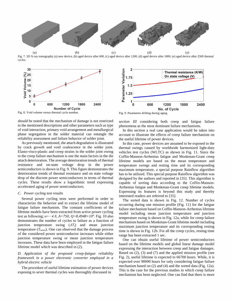
Fig. 7. 3D X-ray tomography (a) new device, (b) aged device after 600, (c) aged device after 1200, (d) aged device after 1800, (e) aged device after 2500 thermal
cycles.
Fig. 8. Void volume versus thermal cycle number.
should be noted that the mechanism of damage is not restricted
to the mentioned descriptions and other parameters such as type
of void interaction, primary void arrangement and metallurgical
phase segregation in the solder material can entangle the
reliability assessment and failure behavior of solder joint.
As previously mentioned, die attach degradation is illustrated
by crack growth and void coalescence in the solder joint.
Elasto-visco-plastic and creep strains in the solder joint owing
to the creep failure mechanism is one the main factors in the die
attach deterioration. The average deterioration trends of thermal
resistance and on-state voltage drop in the power
semiconductors is shown in Fig. 9. This figure demonstrates the
deterioration trends of thermal resistance and on state voltage
drop of the discrete power semiconductors in terms of thermal
cycles. These results show a logarithmic trend expressing
accelerated aging of power semiconductors.
C. Power cycling test results
Several power cycling tests were performed in order to
characterize the behavior and to extract the lifetime model of
fatigue failure mechanism. The constant coefficients of the
lifetime models have been extracted from active power cycling
test as following; α=−4.8, A=750, Q=8.4948×10⁴. Fig. 10 also
demonstrates the number of cycles to failure as a function of
junction temperature swing (ΔTj) and mean junction
temperature (Tmean). One can observed that the damage process
of the considered power semiconductor increases while either
junction temperature swing or mean junction temperature
increases. These data have been employed in the fatigue failure
lifetime model which was described in (2).
D. Application of the proposed creep-fatigue reliability
framework in a power electronic converter employed in a
hybrid electric vehicle
The procedure of useful lifetime estimation of power devices
exposing to sever thermal cycles was thoroughly discussed in
Fig. 9. Parameters drifting during aging.
section III considering both creep and fatigue failure
phenomena as the most dominant failure mechanisms.
In this section a real case application would be taken into
account to illustrate the effects of creep failure mechanism on
the useful lifetime of power devices.
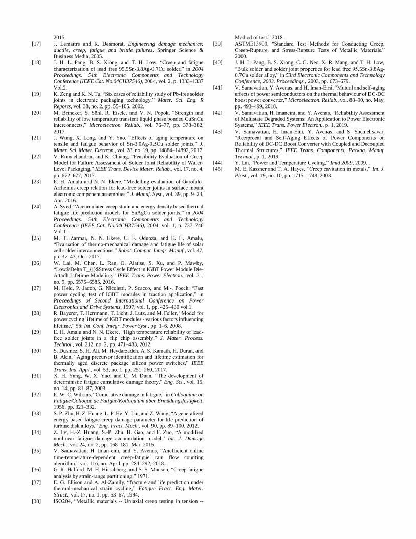
In this case, power devices are assumed to be exposed to the
thermal swings caused by worldwide harmonized light-duty
vehicles test cycles (WLTC) as shown in Fig. 11. Since the
Coffin-Manson-Arrhenius fatigue and Monkman-Grant creep
lifetime models are based on the mean temperature and
temperature swings and resting time and its corresponding
maximum temperature, a special purpose Rainflow algorithm
has to be utilized. This special purpose Rainflow algorithm was
designed by the authors and reported in [35]. This algorithm is
capable of sorting data according to the Coffin-Manson-
Arrhenius fatigue and Monkman-Grant creep lifetime models.
Expressing its features is beyond this study and thereby
interested readers are referred to [35].
The sorted data is shown in Fig. 12. Number of cycles
occurring during one mission profile (Fig. 11) for the fatigue
failure mechanism based on Coffin-Manson-Arrhenius lifetime
model including mean junction temperature and junction
temperature swing is shown in Fig. 12a, while for creep failure
mechanism based on Monkman-Grant lifetime model including
maximum junction temperature and its corresponding resting
time is shown in Fig. 12b. For all the creep cycles, resting time
range has been extracted 1 sec.
One can obtain useful lifetime of power semiconductors
based on the lifetime models and global linear damage model
expressing the interaction between creep and fatigue damages.
Based on (2), (3) and (7) and the applied mission profile (see
Fig. 2), useful lifetime is expected to 66700 hours. While, it is
expected over 90000 hours for only considering fatigue failure
mechanism based on (2) and (4) and the sorted data (Fig. 12a).
This is the case for the previous studies in which creep failure
mechanism has been neglected. One can find that there is more
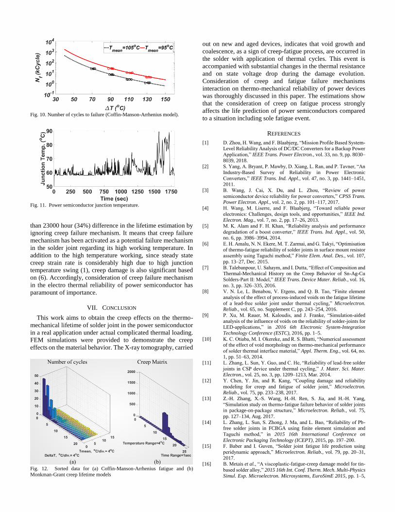
Fig. 10. Number of cycles to failure (Coffin-Manson-Arrhenius model).
Fig. 11. Power semiconductor junction temperature.
than 23000 hour (34%) difference in the lifetime estimation by
ignoring creep failure mechanism. It means that creep failure
mechanism has been activated as a potential failure mechanism
in the solder joint regarding its high working temperature. In
addition to the high temperature working, since steady state
creep strain rate is considerably high due to high junction
temperature swing (1), creep damage is also significant based
on (6). Accordingly, consideration of creep failure mechanism
in the electro thermal reliability of power semiconductor has
paramount of importance.
VII. CONCLUSION
This work aims to obtain the creep effects on the thermo-
mechanical lifetime of solder joint in the power semiconductor
in a real application under actual complicated thermal loading.
FEM simulations were provided to demonstrate the creep
effects on the material behavior. The X-ray tomography, carried
Fig. 12. Sorted data for (a) Coffin-Manson-Arrhenius fatigue and (b)
Monkman-Grant creep lifetime models
out on new and aged devices, indicates that void growth and
coalescence, as a sign of creep-fatigue process, are occurred in
the solder with application of thermal cycles. This event is
accompanied with substantial changes in the thermal resistance
and on state voltage drop during the damage evolution.
Consideration of creep and fatigue failure mechanisms
interaction on thermo-mechanical reliability of power devices
was thoroughly discussed in this paper. The estimations show
that the consideration of creep on fatigue process strongly
affects the life prediction of power semiconductors compared
to a situation including sole fatigue event.
REFERENCES
[1] D. Zhou, H. Wang, and F. Blaabjerg, “Mission Profile Based System-Level Reliability Analysis of DC/DC Converters for a Backup Power
Application,” IEEE Trans. Power Electron., vol. 33, no. 9, pp. 8030–
8039, 2018.
[2] S. Yang, A. Bryant, P. Mawby, D. Xiang, L. Ran, and P. Tavner, “An
Industry-Based Survey of Reliability in Power Electronic
Converters,” IEEE Trans. Ind. Appl., vol. 47, no. 3, pp. 1441–1451, 2011.
[3] B. Wang, J. Cai, X. Du, and L. Zhou, “Review of power
semiconductor device reliability for power converters,” CPSS Trans. Power Electron. Appl., vol. 2, no. 2, pp. 101–117, 2017.
[4] H. Wang, M. Liserre, and F. Blaabjerg, “Toward reliable power
electronics: Challenges, design tools, and opportunities,” IEEE Ind. Electron. Mag., vol. 7, no. 2, pp. 17–26, 2013.
[5] M. K. Alam and F. H. Khan, “Reliability analysis and performance
degradation of a boost converter,” IEEE Trans. Ind. Appl., vol. 50, no. 6, pp. 3986–3994, 2014.
[6] E. H. Amalu, N. N. Ekere, M. T. Zarmai, and G. Takyi, “Optimisation
of thermo-fatigue reliability of solder joints in surface mount resistor assembly using Taguchi method,” Finite Elem. Anal. Des., vol. 107,
pp. 13–27, Dec. 2015.
[7] B. Talebanpour, U. Sahaym, and I. Dutta, “Effect of Composition and Thermal-Mechanical History on the Creep Behavior of Sn-Ag-Cu
Solders-Part II: Model,” IEEE Trans. Device Mater. Reliab., vol. 16,
no. 3, pp. 326–335, 2016. [8] V. N. Le, L. Benabou, V. Etgens, and Q. B. Tao, “Finite element
analysis of the effect of process-induced voids on the fatigue lifetime
of a lead-free solder joint under thermal cycling,” Microelectron. Reliab., vol. 65, no. Supplement C, pp. 243–254, 2016.
[9] P. Xu, M. Rauer, M. Kaloudis, and J. Franke, “Simulation-aided
analysis of the influence of voids on the reliability of solder-joints for LED-applications,” in 2016 6th Electronic System-Integration
Technology Conference (ESTC), 2016, pp. 1–5.
[10] K. C. Otiaba, M. I. Okereke, and R. S. Bhatti, “Numerical assessment of the effect of void morphology on thermo-mechanical performance
of solder thermal interface material,” Appl. Therm. Eng., vol. 64, no. 1, pp. 51–63, 2014.
[11] L. Zhang, L. Sun, Y. Guo, and C. He, “Reliability of lead-free solder
joints in CSP device under thermal cycling,” J. Mater. Sci. Mater. Electron., vol. 25, no. 3, pp. 1209–1213, Mar. 2014.
[12] Y. Chen, Y. Jin, and R. Kang, “Coupling damage and reliability
modeling for creep and fatigue of solder joint,” Microelectron. Reliab., vol. 75, pp. 233–238, 2017.
[13] Z.-H. Zhang, X.-S. Wang, H.-H. Ren, S. Jia, and H.-H. Yang,
“Simulation study on thermo-fatigue failure behavior of solder joints in package-on-package structure,” Microelectron. Reliab., vol. 75,
pp. 127–134, Aug. 2017.
[14] L. Zhang, L. Sun, S. Zhong, J. Ma, and L. Bao, “Reliability of Pb-free solder joints in FCBGA using finite element simulation and
Taguchi method,” in 2015 16th International Conference on
Electronic Packaging Technology (ICEPT), 2015, pp. 197–200. [15] F. Baber and I. Guven, “Solder joint fatigue life prediction using
peridynamic approach,” Microelectron. Reliab., vol. 79, pp. 20–31,
2017. [16] B. Metais et al., “A viscoplastic-fatigue-creep damage model for tin-
based solder alloy,” 2015 16th Int. Conf. Therm. Mech. Multi-Physics
Simul. Exp. Microelectron. Microsystems, EuroSimE 2015, pp. 1–5,
2015. [17] J. Lemaitre and R. Desmorat, Engineering damage mechanics:
ductile, creep, fatigue and brittle failures. Springer Science &
Business Media, 2005. [18] J. H. L. Pang, B. S. Xiong, and T. H. Low, “Creep and fatigue
characterization of lead free 95.5Sn-3.8Ag-0.7Cu solder,” in 2004
Proceedings. 54th Electronic Components and Technology Conference (IEEE Cat. No.04CH37546), 2004, vol. 2, p. 1333–1337
Vol.2.
[19] K. Zeng and K. N. Tu, “Six cases of reliability study of Pb-free solder joints in electronic packaging technology,” Mater. Sci. Eng. R
Reports, vol. 38, no. 2, pp. 55–105, 2002.
[20] M. Brincker, S. Söhl, R. Eisele, and V. N. Popok, “Strength and reliability of low temperature transient liquid phase bonded CuSnCu
interconnects,” Microelectron. Reliab., vol. 76–77, pp. 378–382,
2017. [21] J. Wang, X. Long, and Y. Yao, “Effects of aging temperature on
tensile and fatigue behavior of Sn-3.0Ag-0.5Cu solder joints,” J.
Mater. Sci. Mater. Electron., vol. 28, no. 19, pp. 14884–14892, 2017. [22] V. Ramachandran and K. Chiang, “Feasibility Evaluation of Creep
Model for Failure Assessment of Solder Joint Reliability of Wafer-
Level Packaging,” IEEE Trans. Device Mater. Reliab., vol. 17, no. 4,
pp. 672–677, 2017.
[23] E. H. Amalu and N. N. Ekere, “Modelling evaluation of Garofalo-
Arrhenius creep relation for lead-free solder joints in surface mount electronic component assemblies,” J. Manuf. Syst., vol. 39, pp. 9–23,
Apr. 2016. [24] A. Syed, “Accumulated creep strain and energy density based thermal
fatigue life prediction models for SnAgCu solder joints,” in 2004
Proceedings. 54th Electronic Components and Technology Conference (IEEE Cat. No.04CH37546), 2004, vol. 1, p. 737–746
Vol.1.
[25] M. T. Zarmai, N. N. Ekere, C. F. Oduoza, and E. H. Amalu, “Evaluation of thermo-mechanical damage and fatigue life of solar
cell solder interconnections,” Robot. Comput. Integr. Manuf., vol. 47,
pp. 37–43, Oct. 2017. [26] W. Lai, M. Chen, L. Ran, O. Alatise, S. Xu, and P. Mawby,
“Low$\Delta T_{j}$Stress Cycle Effect in IGBT Power Module Die-
Attach Lifetime Modeling,” IEEE Trans. Power Electron., vol. 31, no. 9, pp. 6575–6585, 2016.
[27] M. Held, P. Jacob, G. Nicoletti, P. Scacco, and M.-. Poech, “Fast
power cycling test of IGBT modules in traction application,” in Proceedings of Second International Conference on Power
Electronics and Drive Systems, 1997, vol. 1, pp. 425–430 vol.1.
[28] R. Bayerer, T. Herrmann, T. Licht, J. Lutz, and M. Feller, “Model for power cycling lifetime of IGBT modules - various factors influencing
lifetime,” 5th Int. Conf. Integr. Power Syst., pp. 1–6, 2008.
[29] E. H. Amalu and N. N. Ekere, “High temperature reliability of lead-free solder joints in a flip chip assembly,” J. Mater. Process.
Technol., vol. 212, no. 2, pp. 471–483, 2012.
[30] S. Dusmez, S. H. Ali, M. Heydarzadeh, A. S. Kamath, H. Duran, and B. Akin, “Aging precursor identification and lifetime estimation for
thermally aged discrete package silicon power switches,” IEEE
Trans. Ind. Appl., vol. 53, no. 1, pp. 251–260, 2017. [31] X. H. Yang, W. X. Yao, and C. M. Duan, “The development of
deterministic fatigue cumulative damage theory,” Eng. Sci., vol. 15,
no. 14, pp. 81–87, 2003. [32] E. W. C. Wilkins, “Cumulative damage in fatigue,” in Colloquium on
Fatigue/Colloque de Fatigue/Kolloquium über Ermüdungsfestigkeit,
1956, pp. 321–332. [33] S. P. Zhu, H. Z. Huang, L. P. He, Y. Liu, and Z. Wang, “A generalized
energy-based fatigue-creep damage parameter for life prediction of
turbine disk alloys,” Eng. Fract. Mech., vol. 90, pp. 89–100, 2012. [34] Z. Lv, H.-Z. Huang, S.-P. Zhu, H. Gao, and F. Zuo, “A modified
nonlinear fatigue damage accumulation model,” Int. J. Damage
Mech., vol. 24, no. 2, pp. 168–181, Mar. 2015. [35] V. Samavatian, H. Iman-eini, and Y. Avenas, “Anefficient online
time-temperature-dependent creep-fatigue rain flow counting
algorithm,” vol. 116, no. April, pp. 284–292, 2018. [36] G. R. Halford, M. H. Hirschberg, and S. S. Manson, “Creep fatigue
analysis by strain-range partitioning,” 1971.
[37] E. G. Ellison and A. Al‐Zamily, “fracture and life prediction under thermal‐mechanical strain cycling,” Fatigue Fract. Eng. Mater.
Struct., vol. 17, no. 1, pp. 53–67, 1994.
[38] ISO204, “Metallic materials -- Uniaxial creep testing in tension --
Method of test.” 2018. [39] ASTME13900, “Standard Test Methods for Conducting Creep,
Creep-Rupture, and Stress-Rupture Tests of Metallic Materials.”
2000. [40] J. H. L. Pang, B. S. Xiong, C. C. Neo, X. R. Mang, and T. H. Low,
“Bulk solder and solder joint properties for lead free 95.5Sn-3.8Ag-
0.7Cu solder alloy,” in 53rd Electronic Components and Technology Conference, 2003. Proceedings., 2003, pp. 673–679.
[41] V. Samavatian, Y. Avenas, and H. Iman-Eini, “Mutual and self-aging
effects of power semiconductors on the thermal behaviour of DC-DC boost power converter,” Microelectron. Reliab., vol. 88–90, no. May,
pp. 493–499, 2018.
[42] V. Samavatian, H. Imaneini, and Y. Avenas, “Reliability Assessment of Multistate Degraded Systems: An Application to Power Electronic
Systems,” IEEE Trans. Power Electron., p. 1, 2019.
[43] V. Samavatian, H. Iman-Eini, Y. Avenas, and S. Shemehsavar, “Reciprocal and Self-Aging Effects of Power Components on
Reliability of DC-DC Boost Converter with Coupled and Decoupled
Thermal Structures,” IEEE Trans. Components, Packag. Manuf. Technol., p. 1, 2019.
[44] Y. Lai, “Power and Temperature Cycling,” Imid 2009, 2009. .
[45] M. E. Kassner and T. A. Hayes, “Creep cavitation in metals,” Int. J.
Plast., vol. 19, no. 10, pp. 1715–1748, 2003.
Related Documents


![An Overview of Elevated Temperature Damage Mechanisms ......the thermomechanical fatigue (TMF) behaviors of the [0 ] and [90 ] systems were examined. Failure and damage mechanisms](https://static.cupdf.com/doc/110x72/60fb1ad729eeb616044e0de3/an-overview-of-elevated-temperature-damage-mechanisms-the-thermomechanical.jpg)