Effective thermo-optical enhanced cross-ring resonator MZI interleavers on SOI Junfeng Song 1, 2 * , H. Zhao 2 , Q. Fang 1 , S. H. Tao 1 , T. Y. Liow 1 , M. B. Yu 1 , G. Q. Lo 1 , and D. L. Kwong 1 1 Institute of Microelectronics, A*STAR (Agency for Science, Technology and Research), 11 Science Park Road, Science Park II, Singapore 117685 2 State Key Laboratory on Integrated Opto-electronics, College of Electronic Science and Engineering, Jilin University, 119 Jiefang Road, Changchun 130023, China *[email protected] http://ime.a-star.edu.sg/ Abstract: A cross-ring (CR-) Mach-Zehnder interferometer (MZI) interleaver structure has been proposed and fabricated. It uses an ‘8’ shaped cross-ring resonator to replace the conventional circular ring resonator. Thus, the new structure can have the function of add-signal. Furthermore, a thermo-optical fine tuning has been applied, which improves the crosstalk performance from ~-10 dB to ~-20 dB with 9 V applied on the heater of the 3-dB directional coupler. ©2008 Optical Society of America OCIS codes: (130.3120) Integrated optics device; (230.3990) Microstructure device; (130.2790) Guided waves; (220.0220) Optical design and fabrication; (220.4000) Microstructure fabrication; (230.0230) Optical devices; (230.3990) Microstructure devices; (350.2460) Filters, interference; References and links 1. S. Cao, J. Chen, J. N. Damask, C. R. Doerr, L. Guiziou, G. Harvey, Y. Hibino, H. Li, S. Suzuki, K. Y. Wu, and P. Xie, “Interleaver technology: comparisons and applications requirements,” OFC’ 03 Interleaver Workshop, pp. 1–9, http://www.neophotonics.com/down/2.pdf . 2. H. Arai, H. Nonen, K. Ohira, and T. Chiba, “PLC wavelength splitter for dense WDM transmission system,” Hitachi Cable Review 21, 11–16 (2002), http://www.hitachi-cable.co.jp/ICSFiles/afieldfile/2005/11/29/2_review03.pdf . 3. S. G. Heris, A. Zarifkar, K. Abedi, and M. K. M. Farshi, “Interleavers/deinterleavers based on Michelson- Gires-Tournois interferometers with different structures,” in Proc. Semicond. Electron., Kuala Lumpur, Malaysia (ICSE 2004) 7–9, 573–576 (2004). 4. C. K. Madsen and J. H. Zhao, Optical Filter Design and Analysis –A Signal Processing Approach (Wiley, New York, 1999). 5. B. B. Dingel and M. Izutsu, “Multifunction optical filter with a Michelson–Gires–Tournois interferometer for wavelength-division-multiplexed network system application,” Opt. Lett. 23, 1099–1101 (1998). 6. C. H. Hsieh, R. B. Wang, Z. Q. James Wen, I. McMichael, P. C. Yeh, C. -W. Lee, and W. H. Cheng, “Flat- top interleavers using two Gires–Tournois etalons as phase-dispersive mirrors in a Michelson interferometer,” IEEE Photon. Technol. Lett. 15, 242–244 (2003). 7. J. Zhang, L. R. Liu, and Y. Zhou, “Novel and simple approach for designing lattice form interleaver filter,” Opt. Express 11, 2217–2224 (2003), http://www.opticsinfobase.org/oe/abstract.cfm?URI=oe-11-18-2217 . 8. C.-W. Lee, R. B. Wang, P. C. Yeh, and W.-H. Cheng, “Sagnac interferometer based flat-top birefringent interleaver,” Opt. Express 14, 4636–4643 (2006), http://www.opticsinfobase.org/oe/abstract.cfm?URI=oe-14-11-4636 . 9. Y. Zhang, Q. J. Wang, and T. C. Soh, “Optical interleaver,” US Patent #2005/0271323A1. 10. Q. J. Wang, Y. Zhang, and Y. C. Soh, “Efficient structure for optical interleavers using superimposed chirped fiber Bragg gratings,” IEEE Photon. Technol. Lett. 17, 387–389 (2005). 11. Q. J. Wang, Y. Zhang, and Y. C. Soh, “All-fiber 3 x 3 interleaver design with flat-top passband,” IEEE Photon. Technol. Lett. 16, 168–170 (2004). 12. K. Jinguji and M. Kawachi, “Synthesis of coherent two-port lattice-form optical delay-line circuit,” J. Lightwave Technol. 13, 73–82 (1995). 13. K. Jinguji, “Synthesis of coherent two-port optical delay-line circuit with ring waveguides,” J. Lightwave Technol. 14, 1882–1884 (1996). 14. M. Oguma, T. Kitoh, K. Jinguji, T. Shibata, A. Himeno, and Y. Hibino, “Passband-width broadening #100651 - $15.00 USD Received 26 Aug 2008; revised 18 Oct 2008; accepted 20 Oct 2008; published 15 Dec 2008 (C) 2008 OSA 22 December 2008 / Vol. 16, No. 26 / OPTICS EXPRESS 21476

Welcome message from author
This document is posted to help you gain knowledge. Please leave a comment to let me know what you think about it! Share it to your friends and learn new things together.
Transcript
Effective thermo-optical enhanced cross-ring resonator MZI interleavers on SOI Junfeng Song1, 2 *, H. Zhao2, Q. Fang1, S. H. Tao1, T. Y. Liow 1,
M. B. Yu1, G. Q. Lo1, and D. L. Kwong1
1Institute of Microelectronics, A*STAR (Agency for Science, Technology and Research), 11 Science Park Road, Science Park II, Singapore 117685
2State Key Laboratory on Integrated Opto-electronics, College of Electronic Science and Engineering, Jilin University, 119 Jiefang Road, Changchun 130023, China
*[email protected] http://ime.a-star.edu.sg/
Abstract: A cross-ring (CR-) Mach-Zehnder interferometer (MZI) interleaver structure has been proposed and fabricated. It uses an ‘8’ shaped cross-ring resonator to replace the conventional circular ring resonator. Thus, the new structure can have the function of add-signal. Furthermore, a thermo-optical fine tuning has been applied, which improves the crosstalk performance from ~-10 dB to ~-20 dB with 9 V applied on the heater of the 3-dB directional coupler.
©2008 Optical Society of America
OCIS codes: (130.3120) Integrated optics device; (230.3990) Microstructure device; (130.2790) Guided waves; (220.0220) Optical design and fabrication; (220.4000) Microstructure fabrication; (230.0230) Optical devices; (230.3990) Microstructure devices; (350.2460) Filters, interference;
References and links
1. S. Cao, J. Chen, J. N. Damask, C. R. Doerr, L. Guiziou, G. Harvey, Y. Hibino, H. Li, S. Suzuki, K. Y. Wu, and P. Xie, “Interleaver technology: comparisons and applications requirements,” OFC’ 03 Interleaver Workshop, pp. 1–9, http://www.neophotonics.com/down/2.pdf.
2. H. Arai, H. Nonen, K. Ohira, and T. Chiba, “PLC wavelength splitter for dense WDM transmission system,” Hitachi Cable Review 21, 11–16 (2002), http://www.hitachi-cable.co.jp/ICSFiles/afieldfile/2005/11/29/2_review03.pdf.
3. S. G. Heris, A. Zarifkar, K. Abedi, and M. K. M. Farshi, “Interleavers/deinterleavers based on Michelson- Gires-Tournois interferometers with different structures,” in Proc. Semicond. Electron., Kuala Lumpur, Malaysia (ICSE 2004) 7–9, 573–576 (2004).
4. C. K. Madsen and J. H. Zhao, Optical Filter Design and Analysis –A Signal Processing Approach (Wiley, New York, 1999).
5. B. B. Dingel and M. Izutsu, “Multifunction optical filter with a Michelson–Gires–Tournois interferometer for wavelength-division-multiplexed network system application,” Opt. Lett. 23, 1099–1101 (1998).
6. C. H. Hsieh, R. B. Wang, Z. Q. James Wen, I. McMichael, P. C. Yeh, C. -W. Lee, and W. H. Cheng, “Flat-top interleavers using two Gires–Tournois etalons as phase-dispersive mirrors in a Michelson interferometer,” IEEE Photon. Technol. Lett. 15, 242–244 (2003).
7. J. Zhang, L. R. Liu, and Y. Zhou, “Novel and simple approach for designing lattice form interleaver filter,” Opt. Express 11, 2217–2224 (2003), http://www.opticsinfobase.org/oe/abstract.cfm?URI=oe-11-18-2217.
8. C.-W. Lee, R. B. Wang, P. C. Yeh, and W.-H. Cheng, “Sagnac interferometer based flat-top birefringent interleaver,” Opt. Express 14, 4636–4643 (2006), http://www.opticsinfobase.org/oe/abstract.cfm?URI=oe-14-11-4636.
9. Y. Zhang, Q. J. Wang, and T. C. Soh, “Optical interleaver,” US Patent #2005/0271323A1. 10. Q. J. Wang, Y. Zhang, and Y. C. Soh, “Efficient structure for optical interleavers using superimposed
chirped fiber Bragg gratings,” IEEE Photon. Technol. Lett. 17, 387–389 (2005). 11. Q. J. Wang, Y. Zhang, and Y. C. Soh, “All-fiber 3 x 3 interleaver design with flat-top passband,” IEEE
Photon. Technol. Lett. 16, 168–170 (2004). 12. K. Jinguji and M. Kawachi, “Synthesis of coherent two-port lattice-form optical delay-line circuit,” J.
Lightwave Technol. 13, 73–82 (1995). 13. K. Jinguji, “Synthesis of coherent two-port optical delay-line circuit with ring waveguides,” J. Lightwave
Technol. 14, 1882–1884 (1996). 14. M. Oguma, T. Kitoh, K. Jinguji, T. Shibata, A. Himeno, and Y. Hibino, “Passband-width broadening
#100651 - $15.00 USD Received 26 Aug 2008; revised 18 Oct 2008; accepted 20 Oct 2008; published 15 Dec 2008
(C) 2008 OSA 22 December 2008 / Vol. 16, No. 26 / OPTICS EXPRESS 21476
design for WDM filter with lattice-form interleave filter and arrayed-waveguide gratings,” IEEE Photon. Technol. Lett. 14, 328–330 (2002).
15. S. Bidnyk, A. Balakrishnan, A. Delâge, M. Gao, P. A. Krug, P. Muthukumaran, and M. Pearson, “Novel architecture for design of planar lightwave interleavers,” J. Lightwave Technol. 23, 1435–1440 (2005).
16. C. G. H. Roeloffzen, R. M. de Ridder, G. Sengo, K. Wörhoff, and A. Driessen “Passband flattened interleaver using a Mach-Zehnder interferometer with ring resonator fabricated in SiON waveguide technology,” in Proceedings Symposium of IEEE/LEOS (IEEE, 2002) 32-35, http://leosbenelux.org/symp02/s02p10.pdf.
17. K. Wörhoff, C. G. H. Roeloffzen, R. M. de Ridder, G. Sengo, L. T. H. Hilderink, P. V. Lambeck, and A. Driessen, “Tolerance and application of polarization independent waveguide for communication devices,” in Proceedings Symposium of IEEE/LEOS (IEEE, 2004) 107–110, http://leosbenelux.org/symp04/s04p107.pdf.
18. Z. P. Wang, S. J. Chang, C. Y. Ni, and Y. J. Chen “A high-performance ultracompact optical interleaver based on double-ring assisted Mach–Zehnder interferometer,” IEEE Photon. Technol. Lett. 19, 1072–1074 (2007).
19. J. Song, Q. Fang, S. H. Tao, M. B. Yu, G. Q. Lo, and D. L. Kwong, “Passive ring-assisted Mach-Zehnder interleaver on silicon-on-insulator,” Opt. Express 16, 8359-8365 (2008), http://www.opticsinfobase.org/oe/abstract.cfm?URI=oe-16-12-8359.
20. J. Song, Q. Fang, S. H. Tao, M. B. Yu, G. Q. Lo, and D. L. Kwong, “Proposed silicon wire interleaver structure,” Opt. Express 16, 7849-7859 (2008), http://www.opticsinfobase.org/oe/abstract.cfm?URI=oe-16-11-7849.
21. J. Chon, A. Zeng, P. Peters, B. Jian, A. Luo, and K. Sullivan, “Integrated interleaves technology enables high performance in DWDM systems,” in Proc. Nat. Fiber Optic Eng. Conf., Baltimore, MD, 1410–1420, (2001), http://www.wavesplitter.com/news/articles_pdf/NFOEC01Interleaver.pdf .
22. W. Bogaerts, P. Dumon, D. V. Thourhout, and R. Baets, “Low-loss, low-cross-talk crossings for silicon-on-insulator nanophotonic waveguides,” Opt. Lett. 32, 2801-2803 (2007)
23. H. Yamda, T. Chu, S. Ishida, and Y. Arakawa, “Si Photonic wire waveguide devices,” IEEE J. Sel. Topics Quantum Electron. 12, 1371–1379 (2006).
1. Introduction
Interleaver structure is one of the key devices in future dense wavelength-division multiplexing (DWDM) applications [1-3]. Many optical filters have been investigated [4]. Interleavers were designed and implemented in many varieties, such as the Michelson–Gires–Tournois interferometer (MGTI) [5, 6], bulk birefringent crystals [7, 8], fibers [9-11], and the planar-light-wave circuit (PLC) [12-20]. Among these, the MGTI, the bulk birefringent crystals, and the fibers cannot be integrated with other devices on a chip. On the contrary, the PLC can be compatible with standard complementary metal-oxide-semiconductor technology, compact and cost-effective. Hence, it is an attractive choice for DWDM applications.
In our recent works [19, 20], two 1 × 2 interleaver structures were designed and fabricated based on 300 nm × 300 nm silicon wire waveguide. The device in [19] is a compact ring-resonator Mach-Zehnder interferometer (RR-MZI) structure. It comprises a ring resonator (RR) and a 3-dB directional coupler (DC). Crosstalk ~ -10 dB and PDL ~ -5 dB were achieved. The one in [20] is a ring assisted Mach-Zehnder interferometer (RA-MZI) structure. However, both structures cannot add signals.
In this paper, we are the first to use silicon waveguides to make a cross-ring (CR), and thus reform a 1 × 2 RR-MZI interleaver structure into a 2 × 2 structure. It has add-signal function after this improvement. Meanwhile, a thermo-optical fine tuning function has also been integrated in this new structure. And crosstalk is improved.
2. Cross-ring interleaver structure
The schematic of 1 × 2 RR-MZI interleaver structure is shown in Fig. 1(a). One of the terminals is left floating in the medial of Fig. 1(a). It is difficulty connect with optical fiber, because it is surrounded by other waveguides. Once we use an ‘8’ shape-like CR to replace the ring, the floating terminal will become an add-signal terminal, which is shown in Fig. 1(b). For example, the pass waveguide will transmit odd-channel signals while the drop waveguide transmits even ones. Then, the add-terminal will add the even- and odd-channel signals to the
#100651 - $15.00 USD Received 26 Aug 2008; revised 18 Oct 2008; accepted 20 Oct 2008; published 15 Dec 2008
(C) 2008 OSA 22 December 2008 / Vol. 16, No. 26 / OPTICS EXPRESS 21477
pass- and drop- waveguides, respectively. The add-signal function is shown in Fig. 1(c), where from the upper input terminal to the two output terminals, the device realizes functions of a common interleaver. For example, odd-channel signals will couple out of the upper output waveguide and even-channel signals will couple out of the lower output one. On the contrary, when signals incident to the lower input terminal, the odd-channel signals will go to the lower output terminal and the even-channel signals go to the upper one. Thus, the CR-MZI structure has more function agility [21].
(a) (b)
(c)
Fig. 1. Schematics of the RR-MZI interleaver structures: (a) 1× 2 RR-MZI structure in [20], and (b) The 2× 2 cross-ring RR-MZI structure. CR: cross-ring. (c) The sketch map of add-signal function.
3. Fabrication
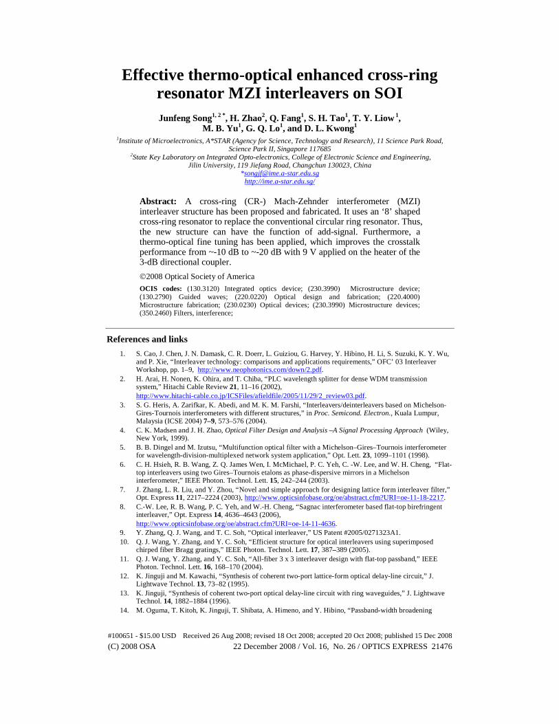
We started the fabrication on a commercially available 200 mm SOI wafer with 240 nm-thick top silicon and 2 μm-thick buried dioxides. The top silicon was thinned down to 200 nm by oxidation. For the cross waveguide in the CR (denoted by an arrow in Fig. 1(b)), the double etching method was adopted [22]. Firstly, we deposited 50 nm undoped silicate glass (USG) oxide as hard mask. The 248 nm deep UV lithography was used to define the device pattern, and an inductively coupled plasma etching system was used to dry etch the hard mask layer. The pattern of the hard mask layer was the same as the device structure except in the cross waveguide region where the waveguide width was expanded from 0.4 μm to 0.8 μm gradually. After a second photo-resist coating, two orthogonal ellipses on the cross waveguide were patterned. We then dry etched the silicon layer, removed the photo-resist, and further dry etched the silicon layer. The Scanning Electron Microscope (SEM) picture of two orthogonal ellipses is shown in Fig. 2(a). The long axis is 6 μm long, and the short axis is 2.5 μm. The Transmission Electron Microscope (TEM) picture of the cross-section of the ellipses with
λ1, λ2, … λ7,λ8,
λ2, λ7
λ1, λ2, λ3, λ5, λ7,
λ2, λ4, λ6,λ7, λ8
Pass Drop Drop Pass
Input Input Add
3-dB DC
RR-DC
(Drop) (Pass)
CR
#100651 - $15.00 USD Received 26 Aug 2008; revised 18 Oct 2008; accepted 20 Oct 2008; published 15 Dec 2008
(C) 2008 OSA 22 December 2008 / Vol. 16, No. 26 / OPTICS EXPRESS 21478
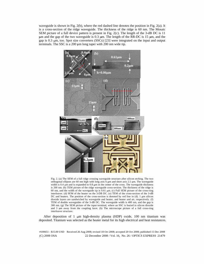
waveguide is shown in Fig. 2(b), where the red dashed line denotes the position in Fig. 2(a). It is a cross-section of the ridge waveguide. The thickness of the ridge is 60 nm. The Mosaic SEM picture of a full device pattern is present in Fig. 2(c). The length of the 3-dB DC is 11 μm and the gap of the two waveguide is 0.3 μm. The length of the RR-DC is 15 μm, and the gap is 0.3 μm, too. Spot size converters (SSCs) [23] were integrated on the input and output terminals. The SSC is a 200 μm long taper with 200 nm wide tip.
Fig. 2. (a) The SEM of a full ridge crossing waveguide structure after silicon etching. The two orthogonal ellipses are 60 nm high with long axis 6 μm and short axis 2.5 μm. The waveguide width is 0.4 μm and is expanded to 0.8 μm in the center of the cross. The waveguide thickness is 200 nm. (b) TEM picture of the ridge waveguide cross-section. The thickness of the ridge is 60 nm, and the width of the waveguide tip is 0.61 μm. (c) Full SEM picture of the cross-ring interleaver. (d) SEM of the heater on the 3-DB DC. (e) TEM of the cross-section of the 3-dB DC and heaters. The position of the cross-section is denoted by red line in (d). 1 μm silicon dioxide layers are sandwiched by waveguide and heater, and heater and air, respectively. (f) TEM of double waveguides of the 3-dB DC. The waveguide width is 400 nm, and the gap is 300 nm. (g) The SEM picture of the input terminal, where an SSC is buried in silicon dioxide and 3 μm away from the coupling facet. (h) The microscope picture of a full cross-ring interleaver structure.
After deposition of 1 μm high-density plasma (HDP) oxide, 100 nm titanium was deposited. Titanium was selected as the heater metal for its high electrical and heat resistances.
Heater
WG
200nm
400nm
300nm
(e) (f) 1μm
1μm
6.2μm
(g)
(d)
(b) (h)
(a)
6μm 2.5μm
0.4μm 0.8μm
(c)
11μm
15μm
0.61μm
h=0.06μm
(b)
0.2μm
#100651 - $15.00 USD Received 26 Aug 2008; revised 18 Oct 2008; accepted 20 Oct 2008; published 15 Dec 2008
(C) 2008 OSA 22 December 2008 / Vol. 16, No. 26 / OPTICS EXPRESS 21479
Lithography was applied again to define the heater pattern on the titanium. The heater was etched as saw-like shape to increase the electrical resistance. The 3-dB DC heaters are shown in Fig. 2(d). The width of the titanium wire is 500 nm and the gap between the wires is also 500 nm. In Fig. 2(e) the TEM picture displays the cross-section of the 3-dB DC and heater shown in Fig. 2(d) and denoted by the red dashed line. The cross-section of the DC is shown in Fig. 2(f). The heaters in the RR-DCs are the same as that of a 3-dB DC. Then, 1 μm HDP oxide was deposited. After the contact holes formation, 750 nm aluminum was deposited. The final process was the deep trench etching. The deep trench is a 3 μm-wide groove. The groove edge is 3 μm away from the waveguide and 2 μm away from the metal (heat or pad). The deep trench will be used to prevent heat diffusion. The depth of the groove is ~100 μm. Such a deep trench is also used for easier fiber coupling subsequently. The micrograph picture of the final device is shown in Fig. 2(g). The dark strip round device is the deep etched groove. A microscope picture of the final cross-ring resonator MZI interleaver is shown in Fig. 2(h). The total length of the device is 2.9 mm.
4. Simulation of waveguide crossing
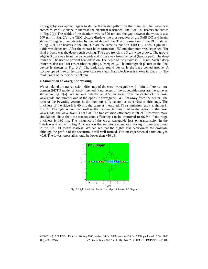
We simulated the transmission efficiency of the cross waveguide with finite difference time domain (FDTD model of RSoft) method. Parameters of the waveguide cross are the same as shown in Fig. 2(a). We set one detector at -4.5 μm away from the center of the cross waveguide and another one at the opposite waveguide +4.5 μm away from the center. The ratio of the Poynting vectors in the monitors is calculated as transmission efficiency. The thickness of the ridge h is 60 nm, the same as measured. The simulation result is shown in Fig. 3. The light is confined well in the incident terminal, but in the region of the cross waveguide, the wave front is not flat. The transmission efficiency is 78.2%. However, more simulations show that, the transmission efficiency can be improved to 96.3% if the ridge thickness is 130 nm. The influence of the cross waveguide loss on transmission in the interleaver is shown in Fig. 4, where γ is the amplitude attenuation for light running a round in the CR. γ=1 means lossless. We can see that the higher loss deteriorates the crosstalk although the profile of the spectrum is still well formed. For our experimental situation, γ is ~0.6. The lowest crosstalk should be lower than ~50 dB.
Fig. 3. Light filed distribution for ridge thickness of 0.06 μm;
h=0.06μm
#100651 - $15.00 USD Received 26 Aug 2008; revised 18 Oct 2008; accepted 20 Oct 2008; published 15 Dec 2008
(C) 2008 OSA 22 December 2008 / Vol. 16, No. 26 / OPTICS EXPRESS 21480
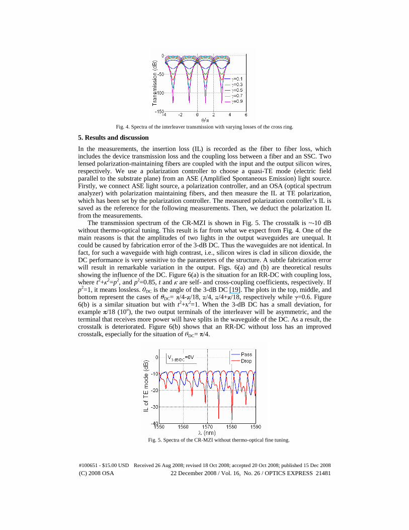
Fig. 4. Spectra of the interleaver transmission with varying losses of the cross ring.
5. Results and discussion
In the measurements, the insertion loss (IL) is recorded as the fiber to fiber loss, which includes the device transmission loss and the coupling loss between a fiber and an SSC. Two lensed polarization-maintaining fibers are coupled with the input and the output silicon wires, respectively. We use a polarization controller to choose a quasi-TE mode (electric field parallel to the substrate plane) from an ASE (Amplified Spontaneous Emission) light source. Firstly, we connect ASE light source, a polarization controller, and an OSA (optical spectrum analyzer) with polarization maintaining fibers, and then measure the IL at TE polarization, which has been set by the polarization controller. The measured polarization controller’s IL is saved as the reference for the following measurements. Then, we deduct the polarization IL from the measurements.
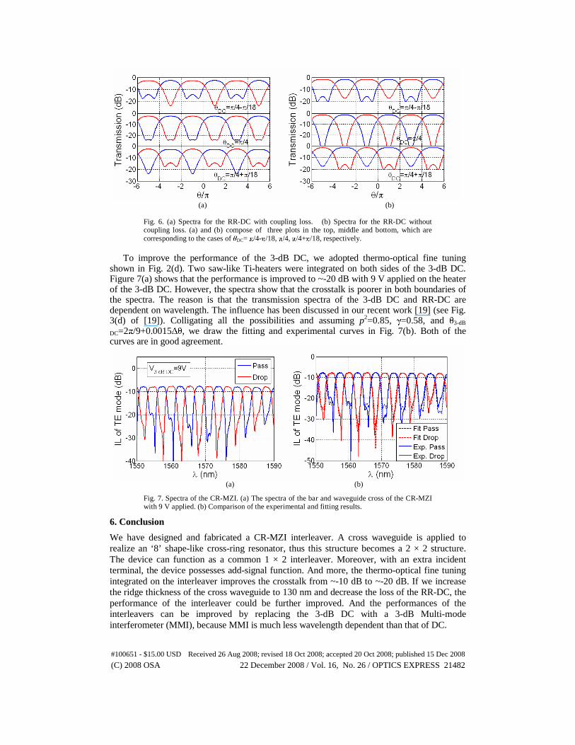
The transmission spectrum of the CR-MZI is shown in Fig. 5. The crosstalk is ~-10 dB without thermo-optical tuning. This result is far from what we expect from Fig. 4. One of the main reasons is that the amplitudes of two lights in the output waveguides are unequal. It could be caused by fabrication error of the 3-dB DC. Thus the waveguides are not identical. In fact, for such a waveguide with high contrast, i.e., silicon wires is clad in silicon dioxide, the DC performance is very sensitive to the parameters of the structure. A subtle fabrication error will result in remarkable variation in the output. Figs. 6(a) and (b) are theoretical results showing the influence of the DC. Figure 6(a) is the situation for an RR-DC with coupling loss, where t2+κ2=p2, and p2=0.85, t and κ are self- and cross-coupling coefficients, respectively. If p2=1, it means lossless. θDC is the angle of the 3-dB DC [19]. The plots in the top, middle, and bottom represent the cases of θDC= π/4-π/18, π/4, π/4+π/18, respectively while γ=0.6. Figure 6(b) is a similar situation but with t2+κ2=1. When the 3-dB DC has a small deviation, for example π/18 (10o), the two output terminals of the interleaver will be asymmetric, and the terminal that receives more power will have splits in the waveguide of the DC. As a result, the crosstalk is deteriorated. Figure 6(b) shows that an RR-DC without loss has an improved crosstalk, especially for the situation of θDC= π/4.
Fig. 5. Spectra of the CR-MZI without thermo-optical fine tuning.
#100651 - $15.00 USD Received 26 Aug 2008; revised 18 Oct 2008; accepted 20 Oct 2008; published 15 Dec 2008
(C) 2008 OSA 22 December 2008 / Vol. 16, No. 26 / OPTICS EXPRESS 21481
(a) (b)
Fig. 6. (a) Spectra for the RR-DC with coupling loss. (b) Spectra for the RR-DC without coupling loss. (a) and (b) compose of three plots in the top, middle and bottom, which are corresponding to the cases of θDC= π/4-π/18, π/4, π/4+π/18, respectively.
To improve the performance of the 3-dB DC, we adopted thermo-optical fine tuning
shown in Fig. 2(d). Two saw-like Ti-heaters were integrated on both sides of the 3-dB DC. Figure 7(a) shows that the performance is improved to ~-20 dB with 9 V applied on the heater of the 3-dB DC. However, the spectra show that the crosstalk is poorer in both boundaries of the spectra. The reason is that the transmission spectra of the 3-dB DC and RR-DC are dependent on wavelength. The influence has been discussed in our recent work [19] (see Fig. 3(d) of [19]). Colligating all the possibilities and assuming p2=0.85, γ=0.58, and θ3-dB
DC=2π/9+0.0015Δθ, we draw the fitting and experimental curves in Fig. 7(b). Both of the curves are in good agreement.
(a) (b)
Fig. 7. Spectra of the CR-MZI. (a) The spectra of the bar and waveguide cross of the CR-MZI with 9 V applied. (b) Comparison of the experimental and fitting results.
6. Conclusion
We have designed and fabricated a CR-MZI interleaver. A cross waveguide is applied to realize an ‘8’ shape-like cross-ring resonator, thus this structure becomes a 2 × 2 structure. The device can function as a common 1 × 2 interleaver. Moreover, with an extra incident terminal, the device possesses add-signal function. And more, the thermo-optical fine tuning integrated on the interleaver improves the crosstalk from ~-10 dB to ~-20 dB. If we increase the ridge thickness of the cross waveguide to 130 nm and decrease the loss of the RR-DC, the performance of the interleaver could be further improved. And the performances of the interleavers can be improved by replacing the 3-dB DC with a 3-dB Multi-mode interferometer (MMI), because MMI is much less wavelength dependent than that of DC.
#100651 - $15.00 USD Received 26 Aug 2008; revised 18 Oct 2008; accepted 20 Oct 2008; published 15 Dec 2008
(C) 2008 OSA 22 December 2008 / Vol. 16, No. 26 / OPTICS EXPRESS 21482
Related Documents