IEEE TRANSACTIONS ON ELECTRON DEVICES, VOL. 62, NO. 3, MARCH 2015 869 Effect of SiO 2 and SiO 2 /SiN x Passivation on the Stability of Amorphous Indium-Gallium Zinc-Oxide Thin-Film Transistors Under High Humidity Md Delwar Hossain Chowdhury, Student Member, IEEE, Mallory Mativenga, Member, IEEE, Jae Gwang Um, Ravi K. Mruthyunjaya, Gregory N. Heiler, Timothy John Tredwell, Senior Member, IEEE , and Jin Jang, Member, IEEE Abstract— We studied the environmental stability of amorphous indium-gallium-zinc-oxide (a-IGZO) thin-film transistors (TFTs) with single-layer (SiO 2 ) and bilayer (SiO 2 /SiN x ) passivation under high-humidity (80%) storage. During the 30 days of investigation, all single-layer passivated TFTs showed negative turn-ON voltage shifts (V ON ), the size of which increased with storing time. The negative V ON is attributed to donor generation inside the active a-IGZO caused by the diffusion of ambient hydrogen/water molecules passing through the SiO 2 passivation layer. The X-ray photoelectron spectroscopy depth profile for the SiO 2 passivated structures confirms that the concentration of oxygen vacancies, which is initially larger at the a-IGZO/SiO 2 interface, compared with the bulk a-IGZO, decreases after 30 days of storage under high humidity. This can be explained as the passivation of oxygen vacancies by diffused hydrogen. On the other hand, all bilayer passivated TFTs showed good air stability at room temperature and high humidity (80%). Index Terms— Amorphous-indium-gallium zinc oxide (a-IGZO), oxide thin-film transistors (TFT) reliability, SiO 2 and SiN x passivation layer, TFT. I. I NTRODUCTION T HE trend in display technology has always been toward large area, optical transparency, and flexibility. As a substitute for hydrogenated amorphous-silicon (a-Si:H) thin-film transistors (TFTs), amorphous indium-gallium zinc-oxide (a-IGZO) TFTs seem to be promising candidates, as they meet most of the requirements needed to achieve these goals. a-IGZO TFTs exhibit 10 times higher field-effect mobility (μ EFF ) compared with a-Si:H TFTs [1], [2], even though a similar manufacturing process is used and both materials are amorphous. Recently, many results for the Manuscript received May 19, 2014; accepted January 10, 2015. Date of publication February 2, 2015; date of current version February 20, 2015. This work was supported in part by the Industrial Strategic Technology Development Program (10045269, Development of Soluble TFT and Pixel Formation Materials/Process Technologies for AMOLED TV) funded by MOTIE/KEIT. The review of this paper was arranged by Editor J. Huang. M. D. H. Chowdhury, M. Mativenga, J. G. Um, and J. Jang are with the Advanced Display Research Center and Department of Information Display, Kyung Hee University, Seoul 130-701, Korea (e-mail: [email protected]). R. K. Mruthyunjaya, G. N. Heiler, and T. J. Tredwell are with Carestream Health Inc., Rochester, NY 14615 USA. Color versions of one or more of the figures in this paper are available online at http://ieeexplore.ieee.org. Digital Object Identifier 10.1109/TED.2015.2392763 electrical stability of a-IGZO TFTs have been published. Most focused on various gate insulator/passivation materials [2]–[7], hydrogen and nitrogen treatments [8], [9] of the a-IGZO back surface, and also time and/or temperature- dependent postfabrication anneals in vacuum, hydrogen, nitrogen, and ambient oxygen [7], [10]–[13]. Amorphous-oxide semiconductors (AOSs) show high sensitivity to hydrogen and oxygen, where the former is commonly considered to be a donor and the latter is an oxygen-vacancy compensator [14]–[16]. These two species are, therefore, used to control the carrier concentration and turn-ON voltage (V ON ) of AOS TFTs. To overcome the dif- fusion of ambient hydrogen/oxygen into the active AOS of a TFT, a good passivation layer is required to protect the devices from external contamination, thus extending the lifetime of the device. Many materials have been used to passivate AOS TFTs [3], [7], and only short-term light and bias stabilities were investigated. For instance, it is a common practice to use SiO 2 rather than SiN x as a gate insulator or passivation material for a-IGZO TFTs because SiO 2 forms less interface trap densities with a-IGZO compared with SiN x [5], [17]. The TFTs with SiO 2 gate insulators and/or passivation have thus been reported to show good stability under positive bias stress (PBS) [18] or negative bias stress [19]. However, the investigation of long-term environmental stability of the SiO 2 passivated TFTs under harsh conditions, such as high humidity, are required to understand the lifetime of the devices. In the present work, we investigated the influence of single-layer (SiO 2 ) and bilayer (SiO 2 /SiN x ) protection layers on the stability of a-IGZO TFTs under high humidity (80%) and room temperature (RT) conditions. It was found that the TFT with the SiO 2 /SiN x bilayer is very stable, but the TFT with the SiO 2 passivation degrades significantly during 30 days of storage. The degradation is related to the diffusion of hydrogen (H) into the a-IGZO layer and the consequential generation of oxygen vacancies, which act as donors. II. EXPERIMENT Bottom-gate, inverted-staggered TFTs with an etch stopper were fabricated on glass substrates. Two sets of samples were prepared. The first set of samples, Sample-A, had a 0018-9383 © 2015 IEEE. Personal use is permitted, but republication/redistribution requires IEEE permission. See http://www.ieee.org/publications_standards/publications/rights/index.html for more information.

Welcome message from author
This document is posted to help you gain knowledge. Please leave a comment to let me know what you think about it! Share it to your friends and learn new things together.
Transcript
IEEE TRANSACTIONS ON ELECTRON DEVICES, VOL. 62, NO. 3, MARCH 2015 869
Effect of SiO2 and SiO2/SiNx Passivation on theStability of Amorphous Indium-Gallium
Zinc-Oxide Thin-Film TransistorsUnder High Humidity
Md Delwar Hossain Chowdhury, Student Member, IEEE, Mallory Mativenga, Member, IEEE,Jae Gwang Um, Ravi K. Mruthyunjaya, Gregory N. Heiler,
Timothy John Tredwell, Senior Member, IEEE ,and Jin Jang, Member, IEEE
Abstract— We studied the environmental stability ofamorphous indium-gallium-zinc-oxide (a-IGZO) thin-filmtransistors (TFTs) with single-layer (SiO2) and bilayer(SiO2/SiNx) passivation under high-humidity (80%) storage.During the 30 days of investigation, all single-layer passivatedTFTs showed negative turn-ON voltage shifts (�VON), the sizeof which increased with storing time. The negative � VON isattributed to donor generation inside the active a-IGZO causedby the diffusion of ambient hydrogen/water molecules passingthrough the SiO2 passivation layer. The X-ray photoelectronspectroscopy depth profile for the SiO2 passivated structuresconfirms that the concentration of oxygen vacancies, which isinitially larger at the a-IGZO/SiO2 interface, compared withthe bulk a-IGZO, decreases after 30 days of storage under highhumidity. This can be explained as the passivation of oxygenvacancies by diffused hydrogen. On the other hand, all bilayerpassivated TFTs showed good air stability at room temperatureand high humidity (80%).
Index Terms— Amorphous-indium-gallium zinc oxide(a-IGZO), oxide thin-film transistors (TFT) reliability, SiO2 andSiNx passivation layer, TFT.
I. INTRODUCTION
THE trend in display technology has always been towardlarge area, optical transparency, and flexibility. As a
substitute for hydrogenated amorphous-silicon (a-Si:H)thin-film transistors (TFTs), amorphous indium-galliumzinc-oxide (a-IGZO) TFTs seem to be promising candidates,as they meet most of the requirements needed to achievethese goals. a-IGZO TFTs exhibit 10 times higher field-effectmobility (μEFF) compared with a-Si:H TFTs [1], [2], eventhough a similar manufacturing process is used and bothmaterials are amorphous. Recently, many results for the
Manuscript received May 19, 2014; accepted January 10, 2015. Date ofpublication February 2, 2015; date of current version February 20, 2015.This work was supported in part by the Industrial Strategic TechnologyDevelopment Program (10045269, Development of Soluble TFT and PixelFormation Materials/Process Technologies for AMOLED TV) funded byMOTIE/KEIT. The review of this paper was arranged by Editor J. Huang.
M. D. H. Chowdhury, M. Mativenga, J. G. Um, and J. Jang are with theAdvanced Display Research Center and Department of Information Display,Kyung Hee University, Seoul 130-701, Korea (e-mail: [email protected]).
R. K. Mruthyunjaya, G. N. Heiler, and T. J. Tredwell are with CarestreamHealth Inc., Rochester, NY 14615 USA.
Color versions of one or more of the figures in this paper are availableonline at http://ieeexplore.ieee.org.
Digital Object Identifier 10.1109/TED.2015.2392763
electrical stability of a-IGZO TFTs have been published.Most focused on various gate insulator/passivationmaterials [2]–[7], hydrogen and nitrogen treatments [8], [9] ofthe a-IGZO back surface, and also time and/or temperature-dependent postfabrication anneals in vacuum, hydrogen,nitrogen, and ambient oxygen [7], [10]–[13].
Amorphous-oxide semiconductors (AOSs) show highsensitivity to hydrogen and oxygen, where the former iscommonly considered to be a donor and the latter is anoxygen-vacancy compensator [14]–[16]. These two speciesare, therefore, used to control the carrier concentration andturn-ON voltage (VON) of AOS TFTs. To overcome the dif-fusion of ambient hydrogen/oxygen into the active AOS of aTFT, a good passivation layer is required to protect the devicesfrom external contamination, thus extending the lifetime ofthe device. Many materials have been used to passivate AOSTFTs [3], [7], and only short-term light and bias stabilitieswere investigated. For instance, it is a common practice touse SiO2 rather than SiNx as a gate insulator or passivationmaterial for a-IGZO TFTs because SiO2 forms less interfacetrap densities with a-IGZO compared with SiNx [5], [17].The TFTs with SiO2 gate insulators and/or passivation havethus been reported to show good stability under positivebias stress (PBS) [18] or negative bias stress [19]. However,the investigation of long-term environmental stability of theSiO2 passivated TFTs under harsh conditions, such as highhumidity, are required to understand the lifetime of the devices.
In the present work, we investigated the influence ofsingle-layer (SiO2) and bilayer (SiO2/SiNx ) protection layerson the stability of a-IGZO TFTs under high humidity (80%)and room temperature (RT) conditions. It was found thatthe TFT with the SiO2/SiNx bilayer is very stable, but theTFT with the SiO2 passivation degrades significantly during30 days of storage. The degradation is related to the diffusionof hydrogen (H) into the a-IGZO layer and the consequentialgeneration of oxygen vacancies, which act as donors.
II. EXPERIMENT
Bottom-gate, inverted-staggered TFTs with an etch stopperwere fabricated on glass substrates. Two sets of sampleswere prepared. The first set of samples, Sample-A, had a
0018-9383 © 2015 IEEE. Personal use is permitted, but republication/redistribution requires IEEE permission.See http://www.ieee.org/publications_standards/publications/rights/index.html for more information.
870 IEEE TRANSACTIONS ON ELECTRON DEVICES, VOL. 62, NO. 3, MARCH 2015
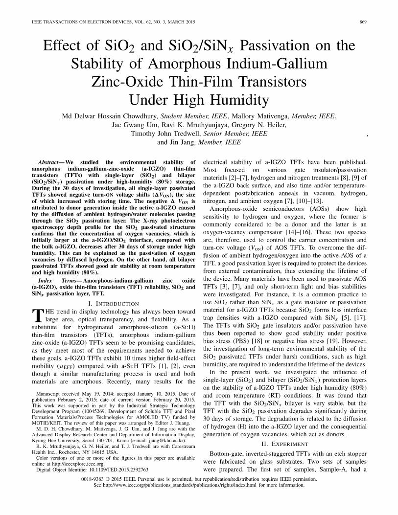
Fig. 1. Cross-sectional view of a-IGZO TFT with (a) single-layer SiO2 asthe passivation layer (Sample-A) and (b) bilayer SiNx /SiO2 as the passivationlayer (Sample-B).
200-nm-thick SiO2 passivation layer. The second set,Sample-B, had a double passivation layer consisting ofSiO2 and SiNx . The thickness of the SiO2 in Sample-B was 150 nm and that of the SiNx was 100 nm. Theschematic cross sections of Sample-A and Sample-B areshown in Fig. 1(a) and (b), respectively. For both samples,a 200-nm-thick SiO2 layer is used as the gate insulator. Thefabrication process begins with deposition by the sputteringof a 150-nm-thick Mo layer that is patterned by wet etch toform the gate electrode. This is followed by the deposition ofthe gate dielectrics by plasma-enhanced chemical vapor depo-sition (PECVD) at 380 °C. The active layer is a 20-nm-thicka-IGZO layer, which is deposited on top of the gate insulator,by sputtering, at 200 °C, using a polycrystalline IGZO target(InO3:Ga2O3:ZnO = 1:1:1 mol %) in an Ar and O2 gasenvironment (with an Ar:O2 ratio of 4:8). After the depositionof the active layer, a 100-nm-thick PECVD SiO2 layer isdeposited and patterned to form an etch stopper, which is usedto protect the a-IGZO during the formation of the source/drainelectrodes.
The gate insulator, active layer, and etch stopper aredeposited without breaking the vacuum in a cluster-depositiontool. This ensures clean interfaces at the back and frontchannel, as the a-IGZO is protected immediately after depo-sition without exposure to air. Note that breaking the vacuumbefore depositing a protective layer on the a-IGZO may lead tosignificant environmental contamination because the a-IGZOis exposed to air when the sample is moved from one place toanother. After the formation of an active island, 150-nm-thickMo is deposited by sputtering at 200 °C and patterned bya wet-etch process, which uses an HNO3-based Mo etchantto form the source/drain electrodes. The fabrication processis completed with the deposition of the passivation layers byPECVD at 200 °C.
The X-ray photoelectron spectroscopy (XPS) depth-profilespectra of a stack of thin films exactly matching thedeposition conditions of the TFT stack in Sample-A(glass/SiO2(200 nm)/a-IGZO(80 nm)/SiO2(300 nm)) weremeasured using a PHI 5000 Versa Probe with a base pressureof 6.7 × 10⁻⁸ Pa and monochromated Al Kα radiation
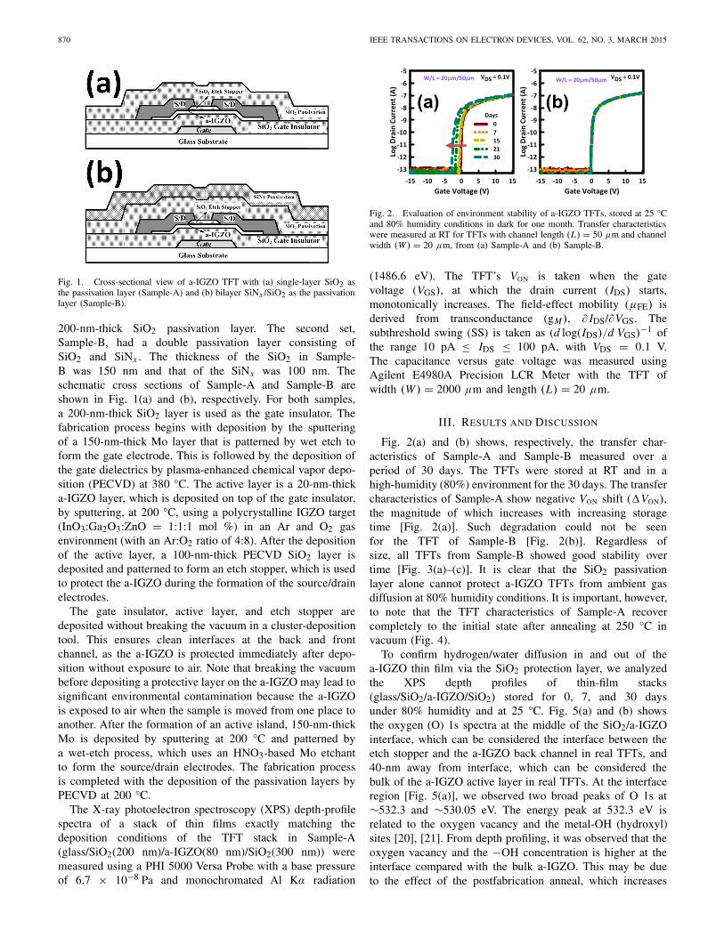
Fig. 2. Evaluation of environment stability of a-IGZO TFTs, stored at 25 °Cand 80% humidity conditions in dark for one month. Transfer characteristicswere measured at RT for TFTs with channel length (L) = 50 μm and channelwidth (W ) = 20 μm, from (a) Sample-A and (b) Sample-B.
(1486.6 eV). The TFT’s VON is taken when the gatevoltage (VGS), at which the drain current (IDS) starts,monotonically increases. The field-effect mobility (μFE) isderived from transconductance (gM), ∂ IDS/∂VGS. Thesubthreshold swing (SS) is taken as (d log(IDS)/d VGS)
−1 ofthe range 10 pA ≤ IDS ≤ 100 pA, with VDS = 0.1 V.The capacitance versus gate voltage was measured usingAgilent E4980A Precision LCR Meter with the TFT ofwidth (W ) = 2000 μm and length (L) = 20 μm.
III. RESULTS AND DISCUSSION
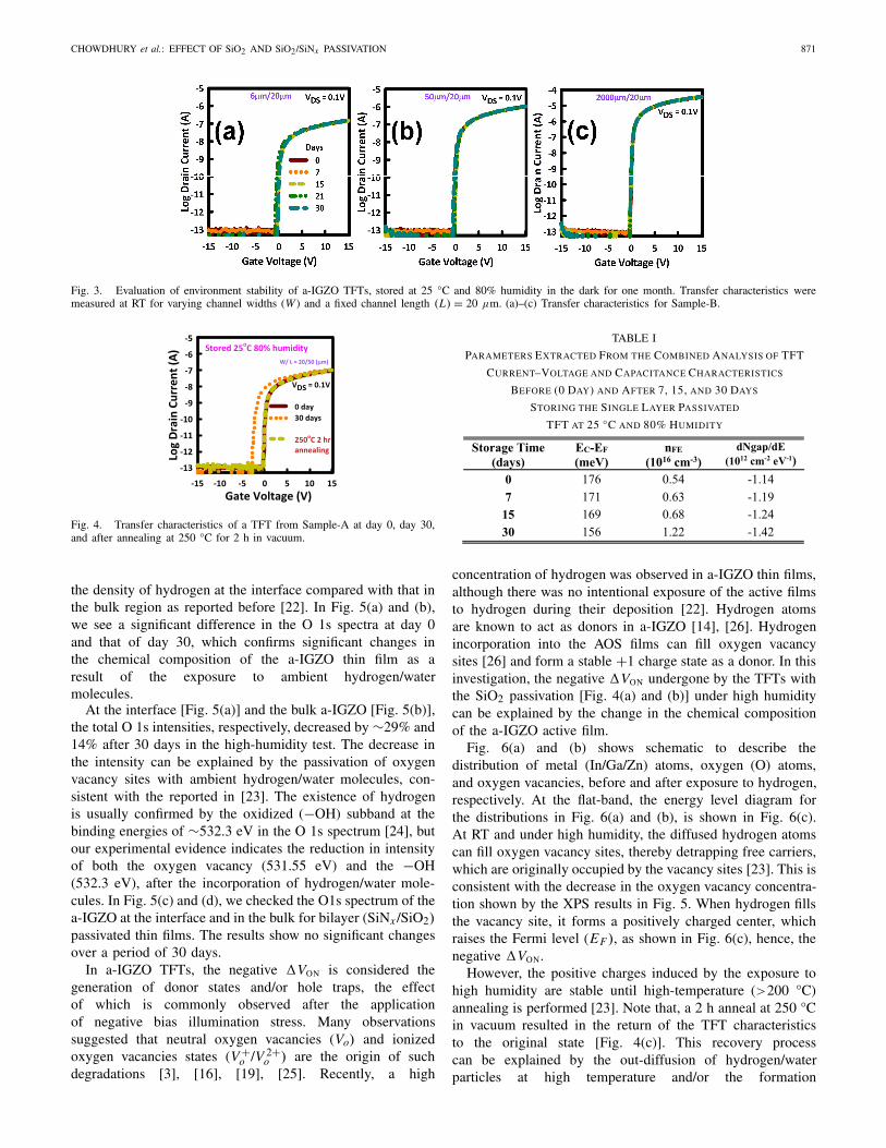
Fig. 2(a) and (b) shows, respectively, the transfer char-acteristics of Sample-A and Sample-B measured over aperiod of 30 days. The TFTs were stored at RT and in ahigh-humidity (80%) environment for the 30 days. The transfercharacteristics of Sample-A show negative VON shift (�VON),the magnitude of which increases with increasing storagetime [Fig. 2(a)]. Such degradation could not be seenfor the TFT of Sample-B [Fig. 2(b)]. Regardless ofsize, all TFTs from Sample-B showed good stability overtime [Fig. 3(a)–(c)]. It is clear that the SiO2 passivationlayer alone cannot protect a-IGZO TFTs from ambient gasdiffusion at 80% humidity conditions. It is important, however,to note that the TFT characteristics of Sample-A recovercompletely to the initial state after annealing at 250 °C invacuum (Fig. 4).
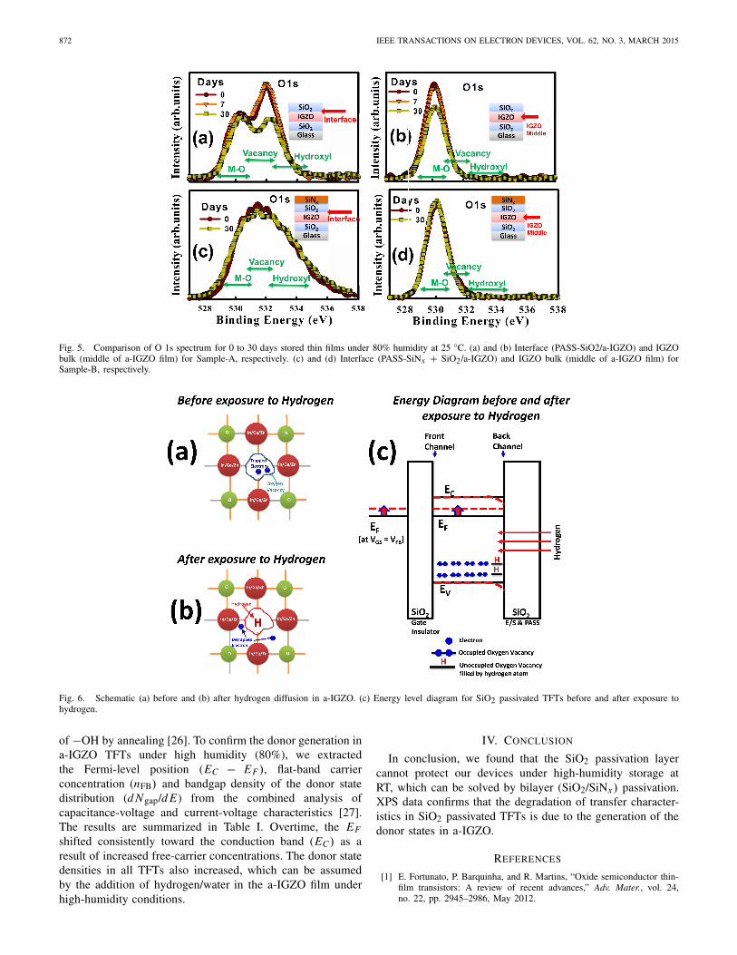
To confirm hydrogen/water diffusion in and out of thea-IGZO thin film via the SiO2 protection layer, we analyzedthe XPS depth profiles of thin-film stacks(glass/SiO2/a-IGZO/SiO2) stored for 0, 7, and 30 daysunder 80% humidity and at 25 °C. Fig. 5(a) and (b) showsthe oxygen (O) 1s spectra at the middle of the SiO2/a-IGZOinterface, which can be considered the interface between theetch stopper and the a-IGZO back channel in real TFTs, and40-nm away from interface, which can be considered thebulk of the a-IGZO active layer in real TFTs. At the interfaceregion [Fig. 5(a)], we observed two broad peaks of O 1s at∼532.3 and ∼530.05 eV. The energy peak at 532.3 eV isrelated to the oxygen vacancy and the metal-OH (hydroxyl)sites [20], [21]. From depth profiling, it was observed that theoxygen vacancy and the −OH concentration is higher at theinterface compared with the bulk a-IGZO. This may be dueto the effect of the postfabrication anneal, which increases
CHOWDHURY et al.: EFFECT OF SiO2 AND SiO2/SiNx PASSIVATION 871
Fig. 3. Evaluation of environment stability of a-IGZO TFTs, stored at 25 °C and 80% humidity in the dark for one month. Transfer characteristics weremeasured at RT for varying channel widths (W ) and a fixed channel length (L) = 20 μm. (a)–(c) Transfer characteristics for Sample-B.
Fig. 4. Transfer characteristics of a TFT from Sample-A at day 0, day 30,and after annealing at 250 °C for 2 h in vacuum.
the density of hydrogen at the interface compared with that inthe bulk region as reported before [22]. In Fig. 5(a) and (b),we see a significant difference in the O 1s spectra at day 0and that of day 30, which confirms significant changes inthe chemical composition of the a-IGZO thin film as aresult of the exposure to ambient hydrogen/watermolecules.
At the interface [Fig. 5(a)] and the bulk a-IGZO [Fig. 5(b)],the total O 1s intensities, respectively, decreased by ∼29% and14% after 30 days in the high-humidity test. The decrease inthe intensity can be explained by the passivation of oxygenvacancy sites with ambient hydrogen/water molecules, con-sistent with the reported in [23]. The existence of hydrogenis usually confirmed by the oxidized (−OH) subband at thebinding energies of ∼532.3 eV in the O 1s spectrum [24], butour experimental evidence indicates the reduction in intensityof both the oxygen vacancy (531.55 eV) and the −OH(532.3 eV), after the incorporation of hydrogen/water mole-cules. In Fig. 5(c) and (d), we checked the O1s spectrum of thea-IGZO at the interface and in the bulk for bilayer (SiNx /SiO2)passivated thin films. The results show no significant changesover a period of 30 days.
In a-IGZO TFTs, the negative �VON is considered thegeneration of donor states and/or hole traps, the effectof which is commonly observed after the applicationof negative bias illumination stress. Many observationssuggested that neutral oxygen vacancies (Vo) and ionizedoxygen vacancies states (V +
o /V 2+o ) are the origin of such
degradations [3], [16], [19], [25]. Recently, a high
TABLE I
PARAMETERS EXTRACTED FROM THE COMBINED ANALYSIS OF TFT
CURRENT–VOLTAGE AND CAPACITANCE CHARACTERISTICS
BEFORE (0 DAY) AND AFTER 7, 15, AND 30 DAYS
STORING THE SINGLE LAYER PASSIVATED
TFT AT 25 °C AND 80% HUMIDITY
concentration of hydrogen was observed in a-IGZO thin films,although there was no intentional exposure of the active filmsto hydrogen during their deposition [22]. Hydrogen atomsare known to act as donors in a-IGZO [14], [26]. Hydrogenincorporation into the AOS films can fill oxygen vacancysites [26] and form a stable +1 charge state as a donor. In thisinvestigation, the negative �VON undergone by the TFTs withthe SiO2 passivation [Fig. 4(a) and (b)] under high humiditycan be explained by the change in the chemical compositionof the a-IGZO active film.
Fig. 6(a) and (b) shows schematic to describe thedistribution of metal (In/Ga/Zn) atoms, oxygen (O) atoms,and oxygen vacancies, before and after exposure to hydrogen,respectively. At the flat-band, the energy level diagram forthe distributions in Fig. 6(a) and (b), is shown in Fig. 6(c).At RT and under high humidity, the diffused hydrogen atomscan fill oxygen vacancy sites, thereby detrapping free carriers,which are originally occupied by the vacancy sites [23]. This isconsistent with the decrease in the oxygen vacancy concentra-tion shown by the XPS results in Fig. 5. When hydrogen fillsthe vacancy site, it forms a positively charged center, whichraises the Fermi level (EF ), as shown in Fig. 6(c), hence, thenegative �VON.
However, the positive charges induced by the exposure tohigh humidity are stable until high-temperature (>200 °C)annealing is performed [23]. Note that, a 2 h anneal at 250 °Cin vacuum resulted in the return of the TFT characteristicsto the original state [Fig. 4(c)]. This recovery processcan be explained by the out-diffusion of hydrogen/waterparticles at high temperature and/or the formation
872 IEEE TRANSACTIONS ON ELECTRON DEVICES, VOL. 62, NO. 3, MARCH 2015
Fig. 5. Comparison of O 1s spectrum for 0 to 30 days stored thin films under 80% humidity at 25 °C. (a) and (b) Interface (PASS-SiO2/a-IGZO) and IGZObulk (middle of a-IGZO film) for Sample-A, respectively. (c) and (d) Interface (PASS-SiNx + SiO2/a-IGZO) and IGZO bulk (middle of a-IGZO film) forSample-B, respectively.
Fig. 6. Schematic (a) before and (b) after hydrogen diffusion in a-IGZO. (c) Energy level diagram for SiO2 passivated TFTs before and after exposure tohydrogen.
of −OH by annealing [26]. To confirm the donor generation ina-IGZO TFTs under high humidity (80%), we extractedthe Fermi-level position (EC − EF ), flat-band carrierconcentration (nFB) and bandgap density of the donor statedistribution (d Ngap/d E) from the combined analysis ofcapacitance-voltage and current-voltage characteristics [27].The results are summarized in Table I. Overtime, the EF
shifted consistently toward the conduction band (EC) as aresult of increased free-carrier concentrations. The donor statedensities in all TFTs also increased, which can be assumedby the addition of hydrogen/water in the a-IGZO film underhigh-humidity conditions.
IV. CONCLUSION
In conclusion, we found that the SiO2 passivation layercannot protect our devices under high-humidity storage atRT, which can be solved by bilayer (SiO2/SiNx ) passivation.XPS data confirms that the degradation of transfer character-istics in SiO2 passivated TFTs is due to the generation of thedonor states in a-IGZO.
REFERENCES
[1] E. Fortunato, P. Barquinha, and R. Martins, “Oxide semiconductor thin-film transistors: A review of recent advances,” Adv. Mater., vol. 24,no. 22, pp. 2945–2986, May 2012.
CHOWDHURY et al.: EFFECT OF SiO2 AND SiO2/SiNx PASSIVATION 873
[2] K. Nomura, H. Ohta, A. Takagi, T. Kamiya, M. Hirano, andH. Hosono, “Room-temperature fabrication of transparent flexiblethin-film transistors using amorphous oxide semiconductors,” Nature,vol. 432, no. 7016, pp. 488–492, Nov. 2004.
[3] M. D. H. Chowdhury, P. Migliorato, and J. Jang, “Light induced insta-bilities in amorphous indium–gallium–zinc–oxide thin-film transistors,”Appl. Phys. Lett., vol. 97, no. 17, p. 173506, Sep. 2010.
[4] K. H. Ji et al., “Comparative study on light-induced bias stress instabilityof IGZO transistors with SiNx and SiO2 gate dielectrics,” IEEE ElectronDevice Lett., vol. 31, no. 12, pp. 1404–1406, Dec. 2010.
[5] J. B. Kim, C. Fuentes-Hernandez, W. J. Potscavage, Jr., X.-H. Zhang, andB. Kippelen, “Low-voltage InGaZnO thin-film transistors with Al2O3gate insulator grown by atomic layer deposition,” Appl. Phys. Lett.,vol. 94, no. 14, p. 142107, Mar. 2009.
[6] Y. S. Chun, S. Chang, and S. Y. Lee, “Effects of gate insulatorson the performance of a-IGZO TFT fabricated at room-temperature,”Microelectron. Eng., vol. 88, no. 7, pp. 1590–1593, Jul. 2011.
[7] K. Nomura, T. Kamiya, and H. Hosono, “Stability and high-frequencyoperation of amorphous In–Ga–Zn–O thin-film transistors with variouspassivation layers,” Thin Solid Films, vol. 520, no. 10, pp. 3778–3782,Mar. 2012.
[8] J. Kim et al., “A study on H2 plasma treatment effect on a-IGZO thinfilm transistor,” J. Mater. Res., vol. 27, no. 17, pp. 2318–2325, Sep. 2012.
[9] J.-C. Jhu et al., “N2O plasma treatment suppressedtemperature-dependent point defects formation with amorphousindium–gallium–zinc-oxide thin film transistors,” ECS Trans., vol. 45,no. 7, pp. 169–178, 2012.
[10] M. D. H. Chowdhury, S. H. Ryu, P. Migliorato, and J. Jang, “Effectof annealing time on bias stress and light-induced instabilities inamorphous indium–gallium–zinc-oxide thin-film transistors,” J. Appl.Phys., vol. 110, no. 11, p. 114503, 2011.
[11] M. D. H. Chowdhury, P. Migliorato, and J. Jang, “Time-temperaturedependence of positive gate bias stress and recovery in amor-phous indium-gallium-zinc-oxide thin-film-transistors,” Appl. Phys.Lett., vol. 98, no. 15, p. 153511, Mar. 2011.
[12] S.-I. Oh, G. Choi, H. Hwang, W. Lu, and J.-H. Jang, “HydrogenatedIGZO thin-film transistors using high-pressure hydrogen annealing,”IEEE Trans. Electron Devices, vol. 60, no. 8, pp. 2537–2541, Aug. 2013.
[13] K. Nomura, T. Kamiya, H. Ohta, M. Hirano, and H. Hosono, “Defectpassivation and homogenization of amorphous oxide thin-film transistorby wet O2 annealing,” Appl. Phys. Lett., vol. 93, no. 19, p. 192107,Oct. 2008.
[14] H. J. Kim et al., “Role of incorporated hydrogen on performance andphoto-bias instability of indium gallium zinc oxide thin film transistors,”J. Phys. D, Appl. Phys., vol. 46, no. 5, p. 055104, 2013.
[15] H.-K. Noh, K. J. Chang, B. Ryu, and W.-J. Lee, “Electronic structureof oxygen-vacancy defects in amorphous In-Ga-Zn-O semiconductors,”Phys. Rev. B, vol. 84, no. 11, p. 115205, Sep. 2011.
[16] K. H. Ji et al., “Effect of high-pressure oxygen annealing on negativebias illumination stress-induced instability of InGaZnO thin film tran-sistors,” Appl. Phys. Lett., vol. 98, no. 10, p. 103509, Feb. 2011.
[17] C.-Y. Jeong et al., “Border trap characterization in amorphousindium-gallium-zinc oxide thin-film transistors with SiOX and SiNXgate dielectrics,” Appl. Phys. Lett., vol. 103, no. 14, p. 142104,Sep. 2013.
[18] M. Mativenga, J. W. Choi, J. H. Hur, H. J. Kim, and J. Jang, “Highlystable amorphous indium–gallium–zinc-oxide thin-film transistor usingan etch-stopper and a via-hole structure,” J. Inf. Display, vol. 12, no. 1,pp. 47–50, Mar. 2011.
[19] J. G. Um, M. Mativenga, P. Migliorato, and J. Jang, “Increase ofinterface and bulk density of states in amorphous-indium-gallium-zinc-oxide thin-film transistors with negative-bias-under-illumination-stresstime,” Appl. Phys. Lett., vol. 101, no. 11, pp. 113504-1–113504-4,Aug. 2012.
[20] A. C. Thompson and D. Vaughan, X-Ray Data Booklet. Berkeley, CA,USA: Lawrence Berkeley National Laboratory, 2001.
[21] Y. Ueoka et al., “Analysis of electronic structure of amorphousInGaZnO/SiO2 interface by angle-resolved X-ray photoelectron spec-troscopy,” J. Appl. Phys., vol. 114, no. 16, p. 163713, Oct. 2013.
[22] K. Nomura, T. Kamiya, and H. Hosono, “Effects of diffusion ofhydrogen and oxygen on electrical properties of amorphous oxidesemiconductor, In-Ga-Zn-O,” ECS J. Solid State Sci. Technol., vol. 2,no. 1, pp. P5–P8, 2013.
[23] Y. Hanyu et al., “Hydrogen passivation of electron trap in amorphousIn-Ga-Zn-O thin-film transistors,” Appl. Phys. Lett., vol. 103, no. 20,p. 202114, Nov. 2013.
[24] J. H. Kang et al., “Mobility enhancement in amorphous InGaZnOthin-film transistors by Ar plasma treatment,” Appl. Phys. Lett., vol. 102,no. 22, p. 222103, Jun. 2013.
[25] M. D. H. Chowdhury, P. Migliorato, and J. Jang, “Temperature depen-dence of negative bias under illumination stress and recovery in amor-phous indium gallium zinc oxide thin film transistors,” Appl. Phys. Lett.,vol. 102, no. 14, p. 143506, Mar. 2013.
[26] H.-K. Noh, J.-S. Park, and K. J. Chang, “Effect of hydrogen incorpora-tion on the negative bias illumination stress instability in amorphousIn-Ga-Zn-O thin-film-transistors,” J. Appl. Phys., vol. 113, no. 6,p. 063712, Jan. 2013.
[27] P. Migliorato, M. Seok, and J. Jang, “Determination of flat band voltagein thin film transistors: The case of amorphous-indium gallium zincoxide,” Appl. Phys. Lett., vol. 100, no. 7, pp. 073506-1–073506-4,Jan. 2012.
Md Delwar Hossain Chowdhury (SM’15) receivedthe M.S. degree in information display engineeringfrom Kyung Hee University, Seoul, Korea, in 2011,where he is currently pursuing the Ph.D. degree ininformation display engineering.
Mallory Mativenga (M’14) received thePh.D. degree in information display from KyungHee University, Seoul, Korea, in 2014.
He is currently a Researcher of InformationDisplay Engineering with Kyung Hee University.
Jae Gwang Um received the M.S. degree ininformation display engineering from Kyung HeeUniversity, Seoul, Korea, in 2013, where he iscurrently pursuing the Ph.D. degree in informationdisplay.
Ravi K. Mruthyunjaya received the B.S. degreein electrical engineering from Clarkson University,Potsdam, NY, USA, and the M.S. degree in electricalengineering from the Rochester Institute ofTechnology, Rochester, NY, USA.
He is currently with Carestream Health, Inc.,Rochester.
Gregory N. Heiler received the B.S. degree from theRochester Institute of Technology, Rochester, NY,USA, in 1985.
He is currently with Carestream Health, Inc.,Rochester, with a specialization on X-ray detectordesign.
874 IEEE TRANSACTIONS ON ELECTRON DEVICES, VOL. 62, NO. 3, MARCH 2015
Timothy John Tredwell (M’79–SM’84) receivedthe Ph.D. degree in solid-state physics from the Uni-versity of Rochester, Rochester, NY, USA, in 1975.
He has been a Senior Research Fellow with Care-stream Health, Inc., Rochester, since 2007.
Jin Jang (M’94) received the Ph.D. degree inphysics from Korea Advanced Institute of Scienceand Technology, Seoul, Korea.
He is currently a Professor of information displayand a director of Advanced Display Research Centerin Kyung Hee University, Seoul and published morethan 450 SCI Journal papers.
Related Documents