JOURNAL OF MICROELECTROMECHANICAL SYSTEMS, VOL. 14, NO. 5, OCTOBER 2005 935 Effect of Nanoscale Heating on Electrical Transport in RF MEMS Switch Contacts Brian D. Jensen, Linda L.-W. Chow, Student Member, IEEE, Kuangwei Huang, Kazuhiro Saitou, Member, IEEE, John L. Volakis, Fellow, IEEE, and Katsuo Kurabayashi, Member, IEEE Abstract—This paper explores contact heating in microelectro- mechanical systems (MEMS) switches with contact spot sizes less than 100 nm in diameter. Experiments are conducted to demonstrate that contact heating causes a drop in contact resis- tance. However, existing theory is shown to over-predict heating for MEMS switch contacts because it does not consider ballistic transport of electrons in the contact. Therefore, we extend the theory and develop a predictive model that shows excellent agreement with the experimental results. It is also observed that mechanical cycling causes an increase in contact resistance. We identify this effect as related to the build-up of an insulating film and demonstrate operational conditions to prevent an increase in contact resistance. The improved understanding of contact behavior gained through our modeling and experiments allows switch performance to be improved. [1424] Index Terms—Electrical contacts, microelectromechanical sys- tems (MEMS), switches. I. INTRODUCTION M ANY examples of metal contact RF MEMS switches are presented in the literature (for example, [1]–[3]). These have demonstrated the excellent performance typical of MEMS switches—high off-state impedance, low on-state impedance,ex- cellent linearity, and low power consumption. This performance makes them attractive alternatives to solid-state switches in mil- itary and commercial radar systems, satellite and wireless com- munications systems, and wireless sensors [4]. In addition to the advantages mentioned above, metal contact switches offer signif- icantly wider bandwidth as compared to capacitive switches, al- lowing them to be used in reconfigurable antennas and circuits in- tended for multiple frequency bands. Understanding the failure of metal contact switches is challenging, however, due to the com- plex interactions between deformation, current flow, and heating at the contact [5]. Still, individual examples of such switches have demonstrated reliable operation to several billion cycles [3], [6]. Several failure mechanisms have been noted for metal contact switches, including adhesion [3], melting, material transport [7], thermally induced explosions related to boiling of the contact Manuscript received September 8, 2004; revised February 15, 2005. This work was supported by the National Science Foundation, a National Defense Science and Engineering Fellowship, and the CIA. Subject Editor H. Fujita. B. D. Jensen is with the Department of Mechanical Engineering, Brigham Young University, Provo, UT 84602 USA (e-mail: [email protected]). L. L.-W. Chow, K. Huang, K. Saitou, and K. Kurabayashi are with the Depart- ment of Mechanical Engineering, University of Michigan, Ann Arbor, MI 48109 USA (e-mail: [email protected]; [email protected]; [email protected]; [email protected]). J. L. Volakis is with the Department of Electrical and Computer Engineering, The Ohio State University, Columbus, OH 43212 USA (e-mail: volakis@ ece.osu.edu). Digital Object Identifier 10.1109/JMEMS.2005.856653 metal [8], and increasing contact resistance [1], [3]. Typically, these failure mechanisms have been noted rather than studied in more depth. For example, an increase in contact resistance as the switch cycles has been reported for both large-scale silver contacts [9] and for MEMS contacts at high cycle numbers [1], [3], but these works have not suggested a hypothesis for the physical cause of the increase. In addition, it is significant that each failure mechanism above relates to the contact behavior. Therefore, improvements in relia- bility and power handling capability require a solid understanding of the physics governing contact formation. However, while con- tact mechanics has been studied extensively over many years, mi- croscale contacts present new challenges. The forces in MEMS contacts (typically tens to hundreds of micro-Newtons) are ap- proximately one thousand times smaller than what has previously been considered as a microcontact force—on the order of 200 mN [10]. Such small forces produce contact spots with size normally comparable to or smaller than the electron mean free path in the material ( 50 nm), leading to additional contact resistance due to boundary scattering of electrons passing though the contact. Heating in contacts due to the passage of current has been studied extensively by Holm [10]. Moreover, finite difference analysis [11] and finite element analysis [12] have both been applied to the heating of contacts in MEMS switches. In all of these works, however, the contact spot size has been assumed to be larger than the electron mean free path. Our experiments suggest that MEMS contacts frequently have spot sizes on the order of or smaller than the mean free path. Such small contact spots are expected to experience reduced heating compared to spots larger than the mean free path. Hence, in this paper we show that existing contact theory sig- nificantly over-predicts contact heating for such small contact spots. We develop improved theory of contact heating for small spots and demonstrate the use of heating for preventing con- tact resistance increase. In multiple experimental results, we show the accuracy of the improved theory. Further, we inves- tigate the causes of contact resistance increase. The resulting understanding allows improved switch operation by keeping re- sistance low. II. EXISTING CONTACT THEORY A significant component of contact resistance is caused by the roughness of the contacting surfaces (see Fig. 1). As the sur- faces come together, high points on each surface make contact, producing real contact at a finite number of asperities. MEMS switch contacts operated under typical conditions are also likely to be covered by a thin insulating film due to process residuals, impurities in the ambient (most likely hydrocarbons), or some 1057-7157/$20.00 © 2005 IEEE

Welcome message from author
This document is posted to help you gain knowledge. Please leave a comment to let me know what you think about it! Share it to your friends and learn new things together.
Transcript

JOURNAL OF MICROELECTROMECHANICAL SYSTEMS, VOL. 14, NO. 5, OCTOBER 2005 935
Effect of Nanoscale Heating on Electrical Transportin RF MEMS Switch Contacts
Brian D. Jensen, Linda L.-W. Chow, Student Member, IEEE, Kuangwei Huang, Kazuhiro Saitou, Member, IEEE,John L. Volakis, Fellow, IEEE, and Katsuo Kurabayashi, Member, IEEE
Abstract—This paper explores contact heating in microelectro-mechanical systems (MEMS) switches with contact spot sizesless than 100 nm in diameter. Experiments are conducted todemonstrate that contact heating causes a drop in contact resis-tance. However, existing theory is shown to over-predict heatingfor MEMS switch contacts because it does not consider ballistictransport of electrons in the contact. Therefore, we extend thetheory and develop a predictive model that shows excellentagreement with the experimental results. It is also observed thatmechanical cycling causes an increase in contact resistance. Weidentify this effect as related to the build-up of an insulating filmand demonstrate operational conditions to prevent an increasein contact resistance. The improved understanding of contactbehavior gained through our modeling and experiments allowsswitch performance to be improved. [1424]
Index Terms—Electrical contacts, microelectromechanical sys-tems (MEMS), switches.
I. INTRODUCTION
MANY examples of metal contact RF MEMS switches arepresented in the literature (for example, [1]–[3]). These
have demonstrated the excellent performance typical of MEMSswitches—highoff-state impedance, lowon-state impedance,ex-cellent linearity, and low power consumption. This performancemakes them attractive alternatives to solid-state switches in mil-itary and commercial radar systems, satellite and wireless com-munications systems, and wireless sensors [4]. In addition to theadvantages mentioned above, metal contact switches offer signif-icantly wider bandwidth as compared to capacitive switches, al-lowing them to be used in reconfigurable antennas and circuits in-tendedformultiple frequencybands.Understanding thefailureofmetal contact switches is challenging, however, due to the com-plex interactions between deformation, current flow, and heatingat the contact [5]. Still, individual examples of such switches havedemonstrated reliable operation to several billion cycles [3], [6].
Several failure mechanisms have been noted for metal contactswitches, including adhesion [3], melting, material transport [7],thermally induced explosions related to boiling of the contact
Manuscript received September 8, 2004; revised February 15, 2005. Thiswork was supported by the National Science Foundation, a National DefenseScience and Engineering Fellowship, and the CIA. Subject Editor H. Fujita.
B. D. Jensen is with the Department of Mechanical Engineering, BrighamYoung University, Provo, UT 84602 USA (e-mail: [email protected]).
L. L.-W. Chow, K. Huang, K. Saitou, and K. Kurabayashi are with the Depart-ment of Mechanical Engineering, University of Michigan, Ann Arbor, MI 48109USA (e-mail: [email protected]; [email protected]; [email protected];[email protected]).
J. L. Volakis is with the Department of Electrical and Computer Engineering,The Ohio State University, Columbus, OH 43212 USA (e-mail: [email protected]).
Digital Object Identifier 10.1109/JMEMS.2005.856653
metal [8], and increasing contact resistance [1], [3]. Typically,these failure mechanisms have been noted rather than studiedin more depth. For example, an increase in contact resistance asthe switch cycles has been reported for both large-scale silvercontacts [9] and for MEMS contacts at high cycle numbers [1],[3], but these works have not suggested a hypothesis for thephysical cause of the increase.
In addition, it is significant that each failure mechanism aboverelates to the contact behavior. Therefore, improvements in relia-bilityandpowerhandlingcapabilityrequireasolidunderstandingof the physics governing contact formation. However, while con-tact mechanics has been studied extensively over many years, mi-croscale contacts present new challenges. The forces in MEMScontacts (typically tens to hundreds of micro-Newtons) are ap-proximatelyone thousand times smaller than what haspreviouslybeenconsidered asa microcontact force—on theorder of200 mN[10]. Such small forces produce contact spots with size normallycomparable to or smaller than the electron mean free path in thematerial ( 50 nm), leading to additional contact resistance dueto boundary scattering of electrons passing though the contact.
Heating in contacts due to the passage of current has beenstudied extensively by Holm [10]. Moreover, finite differenceanalysis [11] and finite element analysis [12] have both beenapplied to the heating of contacts in MEMS switches. In all ofthese works, however, the contact spot size has been assumedto be larger than the electron mean free path. Our experimentssuggest that MEMS contacts frequently have spot sizes on theorder of or smaller than the mean free path. Such small contactspots are expected to experience reduced heating compared tospots larger than the mean free path.
Hence, in this paper we show that existing contact theory sig-nificantly over-predicts contact heating for such small contactspots. We develop improved theory of contact heating for smallspots and demonstrate the use of heating for preventing con-tact resistance increase. In multiple experimental results, weshow the accuracy of the improved theory. Further, we inves-tigate the causes of contact resistance increase. The resultingunderstanding allows improved switch operation by keeping re-sistance low.
II. EXISTING CONTACT THEORY
A significant component of contact resistance is caused bythe roughness of the contacting surfaces (see Fig. 1). As the sur-faces come together, high points on each surface make contact,producing real contact at a finite number of asperities. MEMSswitch contacts operated under typical conditions are also likelyto be covered by a thin insulating film due to process residuals,impurities in the ambient (most likely hydrocarbons), or some
1057-7157/$20.00 © 2005 IEEE

936 JOURNAL OF MICROELECTROMECHANICAL SYSTEMS, VOL. 14, NO. 5, OCTOBER 2005
other source. The presence of this insulating film further limitsmetal-to-metal contact by allowing real contact only at breaksin the film. This creates a restriction causing a larger resistanceacross the contact than results from contact asperities alone.
A contact normally consists of multiple spots of differentsizes. Therefore, prediction of contact spot size distribution isnecessary to fully model contact resistance. Assuming that thespots are sufficiently far apart that they do not interfere signifi-cantly with each other, the resistance of the th spot, , acts inparallel with the others. Hence, the total contact resistance ,accounting for spots, is given by
(1)
Contact surfaces are often modeled using fractal theory, wherethe contact spot distribution follows the power law proposed byMandelbrot [13]. Integrating over each spot gives [14]
(2)
where is the total contact area, is the fractal dimension(a parameter between 2 and 3), and is the area of the largestcontact spot. AFM imaging of the gold surfaces used for ourexperiments showed that for this case is less than 2.05, andtherefore is approximately equal to —indicating that thelargest spot , with the lowest contact resistance, dom-inates the total contact resistance. Then
(3)
Therefore, the contact resistance can be treated as if it werecaused by a single contact spot. By contrast, some previous workin MEMS contacts has estimated that a few tens of asperitieswere in contact [1], [15]. However, this previous work used adifferent fabrication process which resulted in much roughercontact dimples, which would cause the assumption that isnear 2 to be violated. Moreover, the estimate that one asperitydominates the resistance does not preclude the presence of addi-tional contact asperities, so long as the additional contact spotsare sufficiently smaller than the largest spot to contribute littleto the contact conductance.
As current flows, it heats the contact spot to an elevated tem-perature. This heating can be extremely localized, resulting incontact temperatures tens or even hundreds of degrees higherthan the surrounding material. For metal contacts, Holm has ex-pressed the contact spot temperature as a function of contactvoltage as [10]
(4)
Here, is the Lorentz constant andis the ambient temperature. At sufficient contact temperature,
annealing of the contact takes place, reducing the contact hard-ness (a phenomenon known as “contact softening” [10]). More-over, heating of the contact spot may also cause breakdown ordelamination of the insulating film, allowing real contact overa larger area. Either effect is measured as a decrease in contactresistance. This is illustrated in Fig. 1. The published softening
Fig. 1. Illustration of contribution of surface roughness and insulating filmsto contact resistance. Heating due to current flow in the contact spot leads to aresistance decrease caused by material annealing or film breakdown.
Fig. 2. SEM of a gold contact which boiled due to current flow.
Fig. 3. SEM image of a sample contact-type switch. Probe placement is shownfor four-point-probe measurement of contact resistance.
temperature for gold contacts is 100 , corresponding to a con-tact voltage of 70–80 mV for contacts near room temperature[10]. Contact melting or boiling (see Fig. 2) is also possible athigher temperatures. For gold these occur at 1063 and 2817 ,respectively, or about 430 and 900 mV, according to (4).
III. FABRICATION AND EXPERIMENTS
To study contact heating and its effects on contact resistance,we fabricated and tested metal-contact MEMS switches. A SEM

JENSEN et al.: EFFECT OF NANOSCALE HEATING ON ELECTRICAL TRANSPORT IN RF MEMS SWITCH CONTACTS 937
Fig. 4. (a) SEM image of the micromachined dimple, and (b) AFM scan of the gold contact surface.
image of a typical switch is shown in Fig. 3. The switch con-sists of a fixed-fixed beam situated across the ground lines ofa coplanar waveguide. The beam and underlying electrodes aresputtered gold. Electrostatic force is used to pull the beam downuntil the dimple in the center of the beam contacts the central con-ductor of the waveguide. To avoid charging, there is no dielec-tric film coating the actuation electrodes. Instead, the stiffness ofthe beam is relied upon to prevent shorting. The total gap underthe beam is 1.54 , with a dimple height of 1.18 , leavinga distance of 0.36 to travel before contact occurs. The testedbeams had a width of 100 , a thickness of 3.1 , and a lengthof either 400 or 500 . The beam geometry allows four-pointprobe measurements of contact resistance, as illustrated in Fig. 3.The dimples varied in size between 5 5 and , butno difference in contact resistance behavior was seen betweendimples of varying size. SEM imaging of the dimples suggeststhat the bottoms are very flat, without any detectable curvature,as shown in Fig. 4(a). Similarly, AFM imaging of the contactelectrode showed that it has rms roughness of approximately13 nm. A sample AFM scan is shown in Fig. 4(b).
We measured switch pull-down voltage (the voltage justrequired to initiate contact) and ultimate pull-in voltage (thevoltage causing unstable collapse onto the actuation electrodes)and compared them to predictions of a mechanical model toextract Young’s modulus and residual stress. We estimated theYoung’s modulus of our gold film to be 50 5 GPa, with aresidual tensile stress of about 92 6 MPa. Several papers have
Fig. 5. Illustration of fabrication steps.
previously reported estimates between 50–55 GPa for Young’smodulus of microfabricated gold structures, comparing wellwith our measurement [16]–[18]. Contact occurred at approx-imately 55 V for the 500 beam and about 60 V for the400 beam, and catastrophic collapse onto the actuationelectrodes occurs at about 100 and 124 V, respectively.
The contact force in the switches was calculated based onthe measured actuation voltage using a mechanical-electrostaticmodel employing the finite difference method to simulate me-chanical deflection. A reduced-order model based on relationsfor the capacitance of a microstrip line was used to simulatethe electrostatic force [19]. The model was validated by com-parison to simulations using both ANSYS and CoventorWare.
938 JOURNAL OF MICROELECTROMECHANICAL SYSTEMS, VOL. 14, NO. 5, OCTOBER 2005
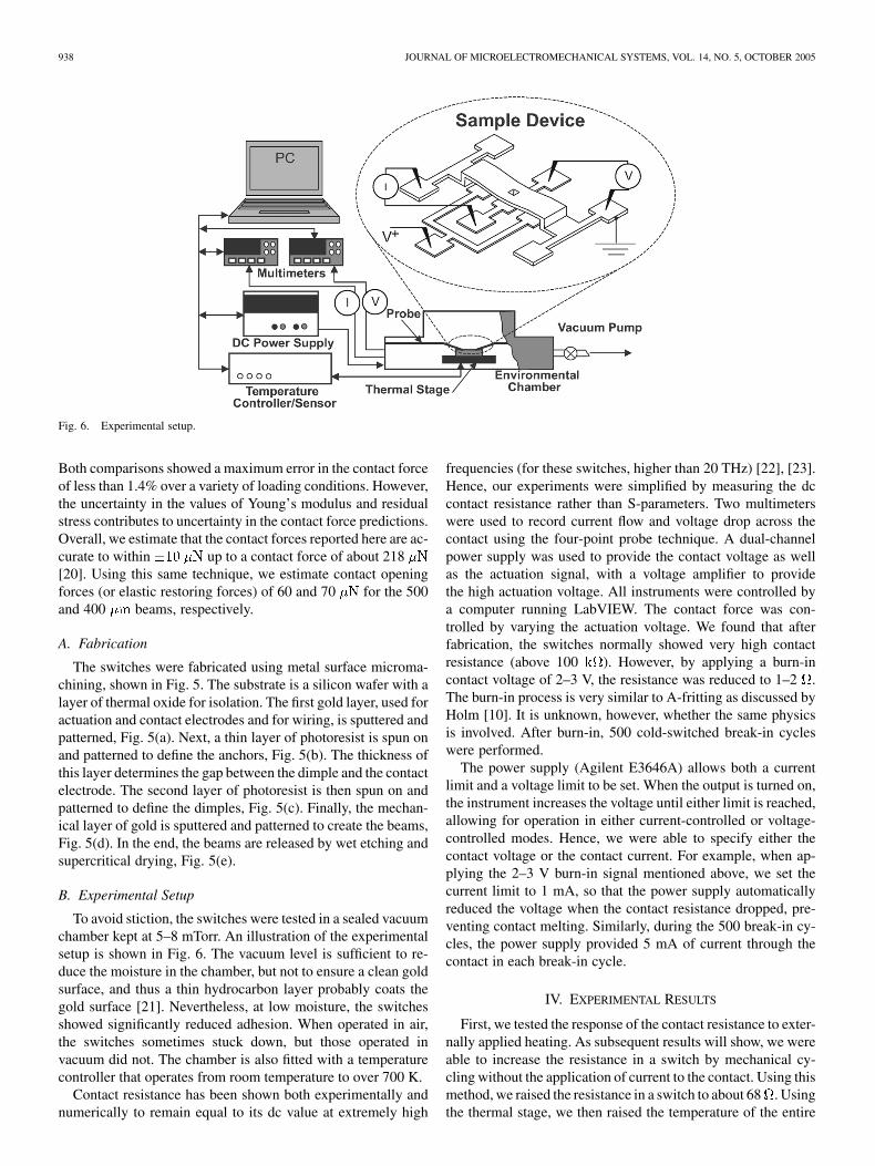
Fig. 6. Experimental setup.
Both comparisons showed a maximum error in the contact forceof less than 1.4% over a variety of loading conditions. However,the uncertainty in the values of Young’s modulus and residualstress contributes to uncertainty in the contact force predictions.Overall, we estimate that the contact forces reported here are ac-curate to within up to a contact force of about 218[20]. Using this same technique, we estimate contact openingforces (or elastic restoring forces) of 60 and 70 for the 500and 400 beams, respectively.
A. Fabrication
The switches were fabricated using metal surface microma-chining, shown in Fig. 5. The substrate is a silicon wafer with alayer of thermal oxide for isolation. The first gold layer, used foractuation and contact electrodes and for wiring, is sputtered andpatterned, Fig. 5(a). Next, a thin layer of photoresist is spun onand patterned to define the anchors, Fig. 5(b). The thickness ofthis layer determines the gap between the dimple and the contactelectrode. The second layer of photoresist is then spun on andpatterned to define the dimples, Fig. 5(c). Finally, the mechan-ical layer of gold is sputtered and patterned to create the beams,Fig. 5(d). In the end, the beams are released by wet etching andsupercritical drying, Fig. 5(e).
B. Experimental Setup
To avoid stiction, the switches were tested in a sealed vacuumchamber kept at 5–8 mTorr. An illustration of the experimentalsetup is shown in Fig. 6. The vacuum level is sufficient to re-duce the moisture in the chamber, but not to ensure a clean goldsurface, and thus a thin hydrocarbon layer probably coats thegold surface [21]. Nevertheless, at low moisture, the switchesshowed significantly reduced adhesion. When operated in air,the switches sometimes stuck down, but those operated invacuum did not. The chamber is also fitted with a temperaturecontroller that operates from room temperature to over 700 K.
Contact resistance has been shown both experimentally andnumerically to remain equal to its dc value at extremely high
frequencies (for these switches, higher than 20 THz) [22], [23].Hence, our experiments were simplified by measuring the dccontact resistance rather than S-parameters. Two multimeterswere used to record current flow and voltage drop across thecontact using the four-point probe technique. A dual-channelpower supply was used to provide the contact voltage as wellas the actuation signal, with a voltage amplifier to providethe high actuation voltage. All instruments were controlled bya computer running LabVIEW. The contact force was con-trolled by varying the actuation voltage. We found that afterfabrication, the switches normally showed very high contactresistance (above 100 ). However, by applying a burn-incontact voltage of 2–3 V, the resistance was reduced to 1–2 .The burn-in process is very similar to A-fritting as discussed byHolm [10]. It is unknown, however, whether the same physicsis involved. After burn-in, 500 cold-switched break-in cycleswere performed.
The power supply (Agilent E3646A) allows both a currentlimit and a voltage limit to be set. When the output is turned on,the instrument increases the voltage until either limit is reached,allowing for operation in either current-controlled or voltage-controlled modes. Hence, we were able to specify either thecontact voltage or the contact current. For example, when ap-plying the 2–3 V burn-in signal mentioned above, we set thecurrent limit to 1 mA, so that the power supply automaticallyreduced the voltage when the contact resistance dropped, pre-venting contact melting. Similarly, during the 500 break-in cy-cles, the power supply provided 5 mA of current through thecontact in each break-in cycle.
IV. EXPERIMENTAL RESULTS
First, we tested the response of the contact resistance to exter-nally applied heating. As subsequent results will show, we wereable to increase the resistance in a switch by mechanical cy-cling without the application of current to the contact. Using thismethod, we raised the resistance in a switch to about 68 . Usingthe thermal stage, we then raised the temperature of the entire
JENSEN et al.: EFFECT OF NANOSCALE HEATING ON ELECTRICAL TRANSPORT IN RF MEMS SWITCH CONTACTS 939
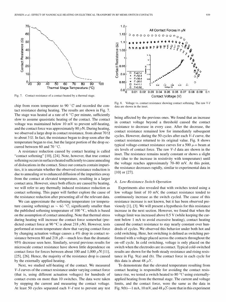
Fig. 7. Contact resistance of a contact heated by a thermal stage.
chip from room temperature to 90 and recorded the con-tact resistance during heating. The results are shown in Fig. 7.The stage was heated at a rate of 6 per minute, sufficientlyslow to assume quasistatic heating of the contact. The contactvoltage was maintained below 10 mV to prevent self-heating,and the contact force was approximately 80 . During heating,we observed a large drop in contact resistance, from about 70to about 3 . In fact, the resistance began to drop soon after thetemperature began to rise, but the largest portion of the drop oc-curred between 60 and 70 .
A resistance reduction caused by contact heating is called“contact softening” [10], [24]. Note, however, that true contactsofteningoccurs insurfacesheatedsufficiently tocauseannealingof dislocations in the contact. Since our contacts contain impuri-ties, it is uncertain whether the observed resistance reduction isdue to annealing or to enhanced diffusion of the impurities awayfrom the contact at elevated temperature, resulting in a largercontact area. However, since both effects are caused by heating,we will refer to any thermally induced resistance reduction ascontact softening. This paper will further explore the cause ofthe resistance reduction after presenting all of the relevant data.
We can approximate the softening temperature (or tempera-ture causing softening) as , significantly smaller thanthe published softening temperature of 100 , which is basedon the assumption of contact annealing. Note that thermal stressduring heating will increase the contact force somewhat (pre-dicted contact force at 90 is about 218 ). However, testsperformed at room temperature show that varying contact forceby changing actuation voltage causes a 4% drop in contact re-sistance between 80 and 218 —much less than the dramatic95% decrease seen here. Similarly, several previous results formicroscale contact resistance have shown little dependence oncontact force for forces between about 100 and 1,000 [11],[25], [26]. Hence, the majority of the resistance drop is causedby the externally applied heating.
Next, we studied self-heating of the contact. We measuredV–I curves of the contact resistance under varying contact force(that is, using different actuation voltages) for hundreds ofcontact events on more than 10 switches. The data were takenby stepping the current and measuring the contact voltage.At least 50 cycles separated each V–I test to prevent any test
Fig. 8. Voltage vs. contact resistance showing contact softening. The raw V-Idata are shown in the inset.
being affected by the previous ones. We found that an increasein contact voltage beyond a threshold caused the contactresistance to decrease in every case. After the decrease, thecontact resistance remained low for immediately subsequentcycles. However, during the 50 cycles after each V–I curve, thecontact resistance returned to its original value. Fig. 8 showstypical voltage-contact resistance curves for a 500 beam atsix levels of contact force. The raw V–I data are shown in theinset. The resistance remains nearly constant or shows a slightrise (due to the increase in resistivity with temperature) untilthe voltage reaches approximately 70–80 mV. At this point,the resistance decreases rapidly, similar to experimental data in[10] or [27].
A. Low-Resistance Switch Operation
Experiments also revealed that with switches tested using alow voltage limit of 10 mV, the contact resistance tended tocontinuously increase as the switch cycled. The cause of thisresistance increase is not known, but it has been observed pre-viously [1], [3]. We will present a hypothesis for this resistanceincrease in the next section. However, we found that when thevoltage limit was increased above 0.5 V (while keeping the cur-rent below 1 mA to avoid excessive heating), contact heatingcaused the contact resistance to stay nearly constant over hun-dreds of cycles. We observed this behavior under both hot andcold switching. Here, hot switching is defined as switching per-formed with a voltage placed across the contacts throughout theon–off cycle. In cold switching, voltage is only placed on theswitch when the electrodes are in contact. Typical cold-switchedresults are shown for the both steady resistance and rising resis-tance in Fig. 9(a) and (b). The contact force in each cycle forthis data is about 48 .
To demonstrate that the elevated temperature resulting fromcontact heating is responsible for avoiding the contact resis-tance rise, we tested a switch heated to 80 using externally-applied heating from the thermal stage. The current and voltagelimits, and the contact force, were the same as the data inFig. 9(b)—1 mA, 10 mV, and 48 (note that in this experiment

940 JOURNAL OF MICROELECTROMECHANICAL SYSTEMS, VOL. 14, NO. 5, OCTOBER 2005
Fig. 9. Cold-switched operation with current limit of 1 mA and voltage limit of(a) 1.3 V (showing steady resistance) and (b) 0.01 V (showing rising resistance).
Fig. 10. Comparison of contact resistance for contacts operated at room-temperature and heated to 80 C.
the actuation voltage was reduced to keep the contact force thesame at elevated temperature). Fig. 10 compares the resultingcontact resistance measurements to the data in Fig. 9(b). Overmore than 200 cycles, while the room-temperature contact resis-tance increases hundreds of times, the heated contact resistanceremains low, showing that heating prevents the increase incontact resistance. While these low-cycle experiments cannotprove that life may be extended in this way, these results suggestthat contact heating may be used to avoid this important failuremechanism for MEMS switches.
TABLE IEXPERIMENTAL RESULTS REGARDING CONTACT RESISTANCE INCREASE
B. Exploration of Resistance Increase
Table I summarizes experimental results that give a better un-derstanding of contact resistance rise. The first two lines give theaverage resistance rise after no operation for 14 and 19 days, re-spectively. In this case, the contact resistance of a switch wasmeasured , and the contact was then opened. For thenext two weeks, neither it nor any of the switches nearby wastested, while the chip remained in the vacuum chamber. On thefourteenth day, the switch was cycled five times with a contactforce of about 48 . The average contact resistance was 5.24higher than the initial contact resistance, with a standard devia-tion of 0.2 . After five further days of no additional operation,the switch was cycled another five times at the same contactforce. In these cycles, the average contact resistance showed anoverall increase of 7.88 (with standard deviation of 0.8 )compared to the initial contact resistance of 2 . Hence, al-though the process was quite slow, the contact resistance in-creased even when no handling of the switches took place. Themost likely cause for such an increase is the gradual build-up orrepair of an insulating film.
The last two lines compare the average contact resistance riseafter 100 cycles for switches tested with a voltage limit of 10 mVand for switches tested with no contact voltage applied. Theseexperiments were performed to test the hypothesis that electro-static force pulled impurities into the contact area, increasingresistance. In each case, three sets of 100 cycles were averaged,with each set beginning after the contact was softened to an ini-tial resistance of 5–10 . As before, the contact force in eachcase was about 48 . The results indicate a statistically in-significant difference. Hence, mechanical cycling alone is animportant factor in the resistance increase.
C. Inconsistencies With Existing Contact Heating Theory
The data in Fig. 8 indicate contact resistance reduction at athreshold voltage of approximately 75–80 mV for an initial con-tact resistance near 1 . This threshold voltage is called the“softening voltage” [10], [24]. (Initial contact resistance hereis the resistance measured at the start, on the linear part of theV–I curve.) However, further testing showed that the softeningvoltage increases as the contact resistance rises. This was testedby measuring V–I curves with a variety of initial contact resis-tance magnitudes. Fig. 11 gives the softening voltages extractedfrom V–I curves of 21 contacts with initial contact resistancesvarying from 0.5 to 336 . The resistances were varied by usingmechanical cycling to raise the resistance and contact heatingto reduce it. The plot shows that the softening voltage increasesfor larger initial contact resistance from about 70 mV at 0.5

JENSEN et al.: EFFECT OF NANOSCALE HEATING ON ELECTRICAL TRANSPORT IN RF MEMS SWITCH CONTACTS 941
Fig. 11. Softening voltage dependence on contact resistance showing theincrease in the softening voltage with higher contact resistance. The linesdrawn on each data point give experimental uncertainty in the measurements.
to over 350 mV at 336 (again, a contact force of about 48was used). These values are all higher than predictions usingexisting theory, as shown by the line at 52 mV. This line repre-sents the voltage prediction from (4) for heating a contact from22 to 65 , the softening temperature measured from Fig. 7.In fact, existing theory gives no explanation for why contactheating should depend on the initial contact resistance. To ex-plain these inconsistencies, we develop below improved theoryfor modeling the contact heating in MEMS-scale contacts. First,we consider further the cause of the resistance increase.
V. DISCUSSION OF RESULTS
While Fig. 10 shows that contact heating prevents immediatecontact resistance rise, the cause of this rapid rise was not ap-parent. We had previously suggested that cold-working of thecontact asperities led to hardening of the metal, increasing con-tact resistance [28]. However, while this may be responsible fora portion of the observed increase, it is unlikely that strain hard-ening can account for a thousand-fold increase like that shownin Fig. 9(b). Since contact resistance scales as the square root ofhardness [24], such a large increase in resistance would requirehardness to increase one million times.
In fact, only the presence of impurities is likely to cause sucha large change in contact resistance. We have already men-tioned that previous work indicated that sputtered gold filmsmost likely retain a thin insulating layer, probably composedof hydrocarbons adsorbed onto the surface [21]. The highcontact resistance of the switches prior to burn-in supports thisidea. However, we believe that actual metal-to-metal contactoccurs after the initial burn-in because the V-I curves are verylinear up to the softening voltage, as will be shown in Fig. 15.In addition, we have found that contacts with lower contactresistance have higher adhesion, suggesting that a larger metalarea is in contact [29].
The results reported in Table I further support the idea that theresistance increase is caused by build-up of an insulating film,with mechanical cycling largely responsible for the build-up.The contact behavior suggested by our results is summarized
Fig. 12. Hypothesis describing contact behavior.
in Fig. 12. Part (a) shows two surfaces in contact. Both surfacesare covered with an insulating film. Placing sufficient voltage onthe contact surfaces causes breakdown of the insulating film, al-lowing current flow, Fig. 12(b). When the surfaces pull apart, thecontact spot is still bare (no film), as depicted in Fig. 12(c). How-ever, randomness in the contact closing process causes the film-free spots to be misaligned in subsequent cycles, Fig. 12(d). Thiscauses the insulating film to be pressed onto the edges of thefilm-free areas, promoting regrowth of the film and leading toincreasing contact resistance. This behavior also explains whythere appears to be just one real contact spot. When the insu-lating film initially breaks down in one spot, the voltage imme-diately drops as current begins to flow, reducing the stress on therest of the film. Based on this hypothesis, the contact resistanceincrease would not be observed in ultra-high vacuum, since ithas been shown that the film is removed in such an environment[21].
VI. THEORY
For a contact radius on the order of the electron mean freepath (about 38 nm in gold [30]) or smaller, the current is con-stricted by both lattice scattering and boundary scattering ofelectrons. For both ohmic constriction and boundary scattering,the contact resistance for a spot of radius is [31]
(5)
where is the mean free path, and is the electrical resistivity.is the Maxwell spreading resistance (the resistance due to
lattice scattering), and is the Sharvin resistance (the addi-tional resistance due to boundary scattering in small constric-tions). Also, is a scaling function. While this equationis well-known, most of the existing work on contact heatingconsiders only the contribution of the Maxwell spreading re-sistance [10], [32]. Even for the smallest contact resistance inFig. 11 of 0.5 , (5) gives a contact radius of 51.8 nm, com-parable to the electron mean free path. (For this calculation,we used a measured resistivity of .) Hence,much of the measured resistance results from boundary scat-tering of electrons. However, boundary-scattered electrons do

942 JOURNAL OF MICROELECTROMECHANICAL SYSTEMS, VOL. 14, NO. 5, OCTOBER 2005
Fig. 13. Half of a contact showing the contact surface, an intermediateisothermal-equipotential surface, and a surface far from the contact spot. Labelsshow the potential and resistance (measured with respect to the contact surface)as well as temperature.
not transfer heat to the metal lattice within the contact constric-tion (see [33]), leading to a reduction in the contact tempera-ture for a given contact voltage. The existing model of contactheating does not include this effect.
In addition, the existing model of (4) assumes that the tem-perature far from the contact spot is equal in each of the con-tacting bodies. This is not true for many MEMS contacts, sincethe small size of the moving contact makes heating of the entiremoving body unlikely. Hence, a difference exists between thesubstrate (at room temperature) and the moving body (at an el-evated temperature). Therefore, understanding of the nanoscalecontact heating requires consideration of both the device-leveltemperature and the extremely localized heating of the contactspot. At the nanometer scale, models relate the real contact sizeand contact voltage with the contact temperature. On the de-vice level, an integrated electrothermal model is necessary todescribe the relationship between current flow and temperature.
A. Asperity Heating Model
The goal of the nanoscale contact heating model is to relatethe contact voltage to the contact spot temperature whileconsidering the effects of contact spot size. The principle dif-ference between the theory presented here and existing theoryis that we assume that heating in the contact is due only to theMaxwell term in (5), .
Greenwood and Williamson have previously shown thatequipotential surfaces are also isothermals in a contact [32].For initial development of the model, we assume that thecontact is symmetric, with maximum temperature at the contactasperity. This assumption will be relaxed later. Hence, weanalyze a half-contact. See Fig. 13 for an illustration, withlabels showing potential, resistance, and temperature at thecontact spot, an arbitrary intermediate isothermal-equipotentialsurface, and on a surface sufficiently far from the contact. Wefurther assume that the potential on an equipotential surfacecan be broken into Maxwell and Sharvin components as
(6)
and are the Maxwell and Sharvin components of re-sistance between the surface and the contact spot, and
is the total resistance in the same volume.Assuming that the Maxwell resistance is the only source of
contact heating, we can write the total heat generated between
the contact spot and any isothermal as . The isothermaldifferential temperature is then
(7)
where is the corresponding differential thermal resistanceof the surface. If we assume that conduction through the metal isthe dominant form of heat transfer through the contact, we canalso compare the differential thermal and electrical resistanceson any equipotential surface via the relation
(8)
Here, and are the effective electrical resistivity andthermal conductivity of the metal accounting for size effects.Substituting (6) and (8) into (7) then gives
(9)
Integrating from the contact spot to the far surface produces
(10)
Unfortunately, the detailed geometry of the contact is re-quired to calculate and . However, we may estimatethe ratio as that of the overall Maxwell resistance tothe overall contact resistance, . Makingthis substitution into (10) and evaluating the integral gives
(11)
The left-hand side of (11) may be evaluated using the Wiede-mann–Franz law. This law states that for metals, ,where and are the material electrical resistivity and thermalconductivity [34]. The Wiedemann–Franz law has been shownto apply even at atomistic length scales, the size of the smallestpossible contact spots, so it applies to the factor as well[35], resulting in
(12)
The only difference between (12) and (4) is the factor .This factor is nearly unity when is small (when is muchlarger than ), and it decreases to nearly zero for large (when
is much smaller than ). Therefore, for a small contact resis-tance, (12) is equal to (4), deviating only when boundary scat-tering contributes to the contact resistance.
Equation (12) gives the asperity temperature assuming bothcontact surfaces are at the same temperature . As describedabove, the moving surface in a MEMS switch is likely to beheated by the passage of current, and so the material in the con-tact surfaces is at different temperatures and (we arbi-trarily choose ). In this case, a constant additional heat

JENSEN et al.: EFFECT OF NANOSCALE HEATING ON ELECTRICAL TRANSPORT IN RF MEMS SWITCH CONTACTS 943
flux will flow through the contact, and so (7) will have an ad-ditional term
(13)
The flux is added if the isothermal surface is in contact body1 (at ) and subtracted in body 2 (at ). Following the samederivation used for (12) leads to
(14)
(15)
Eliminating from both equations yields
(16)
We remark that (16) is identical to (12) when .We also note that (12) has been experimentally validated usingMEMS switch contacts [36].
B. Electrothermal Model
Use of (16) requires knowledge of and , the temper-atures of the contacting bodies. We can assume that the fixedcontact remains at ambient temperature, . However,electrothermal modeling of the switch is required to calculate
, the temperature in the moving contact. The electrothermalmodel used here is described in [37]. Briefly, 2-D finite ele-ment modeling (FEM) is used to solve the heat equation withthe electric current as a heat source. The model includes effectsdue to heat conduction and contact heating, as well as electricaland thermal contact resistance. Convective and radiative heattransfer are ignored because they are insignificant.
C. Comparison to Experimental Data
Using the combination of FEM and (16), we analyzed thedata of Fig. 8 to determine the contact spot temperature andpercent real contact area increase. First, we used the FEM tocalculate the temperature in the beam near the contact. We thencomputed the contact spot temperature using (16). Finding thereal contact area requires knowledge of the change in averageelectrical resistivity as the contact is heated. Holm estimated thatthe average resistivity changes as [10]
(17)
where and are respectively the average and room tempera-ture resistivities and , the difference between thecontact spot temperature and room temperature. We estimatedthe contact spot size for each data point of Fig. 8 using (5) and(17), allowing estimation of the area increase as , whereis the real contact radius and is the initial contact radius (thefirst data point for each V–I curve).
Fig. 14 shows the calculated percent contact area increaseas a function of the predicted contact temperature. The datashow rapidly increasing contact area above about 65 . Thisresult agrees well with the experimental threshold temperature
Fig. 14. Percent increase in contact area as a function of contact spottemperature for the data shown in Fig. 8.
Fig. 15. Four V-I curves with contact temperature isothermals. The expectedsoftening region, 60–80 C, is shaded for emphasis. After becoming nonlinear,the V–I curves follow the shaded isothermals, showing that softening continuesat the same temperature as current increases.
of 60–70 . However, we emphasize again that these temper-atures are well below the published softening temperature forgold of 100 [10]. We believe that the resistance decrease inour experiments is due to the thermal breakdown of bonds be-tween the gold and the insulating film, allowing the film to beeasily pushed aside. Alternatively, it has been shown that goldmelting temperature drops for small gold particles [38]. Hence,it is also possible that softening occurs at reduced temperaturefor small contact spots. Softening at the published softeningtemperature has been linked to annealing, leading to a reduc-tion in hardness of the work-hardened contact spot [10]. We be-lieve that the reason for the disparity is that our measurementsare recording a different physical phenomenon (breakdown ofan insulating film) that seems to dominate contact resistance inlow-force MEMS contacts.
Four V-I curves from the tests summarized in Fig. 11 areshown in Fig. 15 and compared to model predictions of asperitytemperature. The contacts had initial resistance of 2, 17, 50, and336 . Contact temperature isothermals are shown for tempera-tures from 30 to 100 . These isothermal lines were calculated
944 JOURNAL OF MICROELECTROMECHANICAL SYSTEMS, VOL. 14, NO. 5, OCTOBER 2005
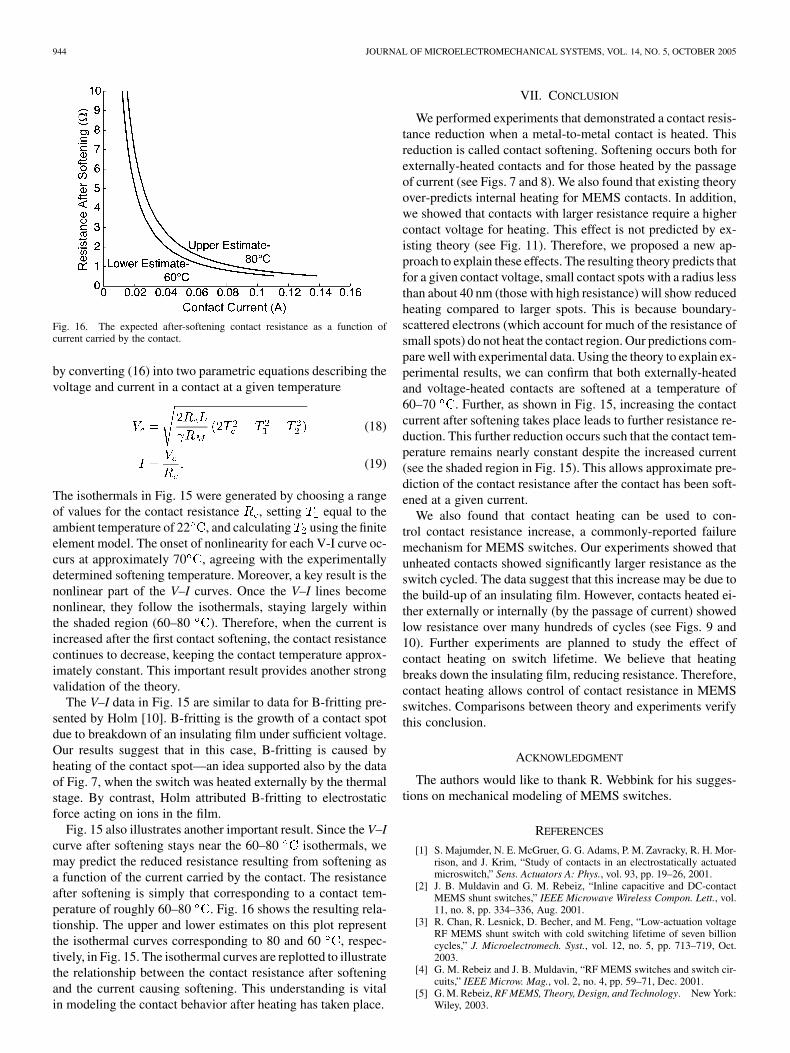
Fig. 16. The expected after-softening contact resistance as a function ofcurrent carried by the contact.
by converting (16) into two parametric equations describing thevoltage and current in a contact at a given temperature
(18)
(19)
The isothermals in Fig. 15 were generated by choosing a rangeof values for the contact resistance , setting equal to theambient temperature of 22 , and calculating using the finiteelement model. The onset of nonlinearity for each V-I curve oc-curs at approximately 70 , agreeing with the experimentallydetermined softening temperature. Moreover, a key result is thenonlinear part of the V–I curves. Once the V–I lines becomenonlinear, they follow the isothermals, staying largely withinthe shaded region (60–80 ). Therefore, when the current isincreased after the first contact softening, the contact resistancecontinues to decrease, keeping the contact temperature approx-imately constant. This important result provides another strongvalidation of the theory.
The V–I data in Fig. 15 are similar to data for B-fritting pre-sented by Holm [10]. B-fritting is the growth of a contact spotdue to breakdown of an insulating film under sufficient voltage.Our results suggest that in this case, B-fritting is caused byheating of the contact spot—an idea supported also by the dataof Fig. 7, when the switch was heated externally by the thermalstage. By contrast, Holm attributed B-fritting to electrostaticforce acting on ions in the film.
Fig. 15 also illustrates another important result. Since the V–Icurve after softening stays near the 60–80 isothermals, wemay predict the reduced resistance resulting from softening asa function of the current carried by the contact. The resistanceafter softening is simply that corresponding to a contact tem-perature of roughly 60–80 . Fig. 16 shows the resulting rela-tionship. The upper and lower estimates on this plot representthe isothermal curves corresponding to 80 and 60 , respec-tively, in Fig. 15. The isothermal curves are replotted to illustratethe relationship between the contact resistance after softeningand the current causing softening. This understanding is vitalin modeling the contact behavior after heating has taken place.
VII. CONCLUSION
We performed experiments that demonstrated a contact resis-tance reduction when a metal-to-metal contact is heated. Thisreduction is called contact softening. Softening occurs both forexternally-heated contacts and for those heated by the passageof current (see Figs. 7 and 8). We also found that existing theoryover-predicts internal heating for MEMS contacts. In addition,we showed that contacts with larger resistance require a highercontact voltage for heating. This effect is not predicted by ex-isting theory (see Fig. 11). Therefore, we proposed a new ap-proach to explain these effects. The resulting theory predicts thatfor a given contact voltage, small contact spots with a radius lessthan about 40 nm (those with high resistance) will show reducedheating compared to larger spots. This is because boundary-scattered electrons (which account for much of the resistance ofsmall spots) do not heat the contact region. Our predictions com-pare well with experimental data. Using the theory to explain ex-perimental results, we can confirm that both externally-heatedand voltage-heated contacts are softened at a temperature of60–70 . Further, as shown in Fig. 15, increasing the contactcurrent after softening takes place leads to further resistance re-duction. This further reduction occurs such that the contact tem-perature remains nearly constant despite the increased current(see the shaded region in Fig. 15). This allows approximate pre-diction of the contact resistance after the contact has been soft-ened at a given current.
We also found that contact heating can be used to con-trol contact resistance increase, a commonly-reported failuremechanism for MEMS switches. Our experiments showed thatunheated contacts showed significantly larger resistance as theswitch cycled. The data suggest that this increase may be due tothe build-up of an insulating film. However, contacts heated ei-ther externally or internally (by the passage of current) showedlow resistance over many hundreds of cycles (see Figs. 9 and10). Further experiments are planned to study the effect ofcontact heating on switch lifetime. We believe that heatingbreaks down the insulating film, reducing resistance. Therefore,contact heating allows control of contact resistance in MEMSswitches. Comparisons between theory and experiments verifythis conclusion.
ACKNOWLEDGMENT
The authors would like to thank R. Webbink for his sugges-tions on mechanical modeling of MEMS switches.
REFERENCES
[1] S. Majumder, N. E. McGruer, G. G. Adams, P. M. Zavracky, R. H. Mor-rison, and J. Krim, “Study of contacts in an electrostatically actuatedmicroswitch,” Sens. Actuators A: Phys., vol. 93, pp. 19–26, 2001.
[2] J. B. Muldavin and G. M. Rebeiz, “Inline capacitive and DC-contactMEMS shunt switches,” IEEE Microwave Wireless Compon. Lett., vol.11, no. 8, pp. 334–336, Aug. 2001.
[3] R. Chan, R. Lesnick, D. Becher, and M. Feng, “Low-actuation voltageRF MEMS shunt switch with cold switching lifetime of seven billioncycles,” J. Microelectromech. Syst., vol. 12, no. 5, pp. 713–719, Oct.2003.
[4] G. M. Rebeiz and J. B. Muldavin, “RF MEMS switches and switch cir-cuits,” IEEE Microw. Mag., vol. 2, no. 4, pp. 59–71, Dec. 2001.
[5] G. M. Rebeiz, RF MEMS, Theory, Design, and Technology. New York:Wiley, 2003.

JENSEN et al.: EFFECT OF NANOSCALE HEATING ON ELECTRICAL TRANSPORT IN RF MEMS SWITCH CONTACTS 945
[6] J. Lampen, S. Majumder, R. Morrison, A. Chaudhry, and J. Maciel,“A wafer-capped, high-lifetime ohmic MEMS RF switch,” Int. J. RFMicrowave Computer-Aided Eng., vol. 14, no. 4, pp. 338–344, Jul.2004.
[7] B. J. Gally, C. C. Abnet, and S. Brown, “Investigation of wear of mi-croelectromechanical contacts,” in Proc. Mat. Res. Soc. Symp., vol. 605,2000, pp. 117–122.
[8] E. J. J. Kruglick and K. S. J. Pister, “Lateral MEMS microcontact con-siderations,” J. Microelectromech. Syst., vol. 8, no. 3, pp. 264–271, Sept.1999.
[9] M. Hasegawa, T. Yamamoto, and K. Sawa, “Significant increase of con-tact resistance of silver contacts by mechanical switching actions,” IEEETrans. Comp., Hybrids, Manufact. Technol., vol. 15, no. 2, pp. 177–183,1992.
[10] R. Holm, Electric Contacts—Theory and Applications, 4th ed. Berlin,Germany: Springer-Verlag, 1967.
[11] D. Hyman and M. Mehregany, “Contact physics of gold microcontactsfor MEMS switches,” IEEE Trans. Comp. Packag. Technol., vol. 22, no.3, pp. 357–364, Sep. 1999.
[12] X. Yan, N. E. McGruer, G. G. Adams, and S. Majumder, “Finite ele-ment analysis of the thermal characteristics of mems switches,” in Proc.12th Int. Conf. on Transducers, Solid-State Sensors, Actuators, and Mi-crosystems, Jun. 2003.
[13] B. B. Mandelbrot, The Fractal Geometry of Nature. New York:Freeman, 1983.
[14] W. Yan and K. Komvopoulos, “Contact analysis of elastic-plastic fractalsurfaces,” J. Appl. Phys., vol. 84, no. 7, pp. 3617–3624, 1998.
[15] S. Majumder, N. E. McGruer, P. M. Zavracky, G. G. Adams, R.H. Morrison, and J. Krim, “Measurement and modeling of surfacemicromachined, electrostatically actuated microswitches,” in Proc.1997 Int. Conf. Solid-State Sensors and Actuators, Jun. 1997, pp.1145–1148.
[16] B. Kracke and B. Damaschke, “Measurement of nanohardness and na-noelasticity of thin gold films with scanning force microscope,” Appl.Phys. Lett., vol. 77, no. 3, pp. 361–363, Jul. 2000.
[17] H. D. Espinosa and B. C. Prorok, “Size effects on the mechanical be-havior of gold thin films,” J. Mat. Sci., vol. 38, pp. 4125–4128, 2003.
[18] H. D. Espinosa, B. C. Prorok, and M. Fischer, “A methodology for de-termining mechanical properties of freestanding thin films and MEMSmaterials,” J. Mechan. Phys. Solids, vol. 51, pp. 47–67, 2003.
[19] F. E. Gardiol, Microstrip Circuits. New York: Wiley, 1994.[20] B. D. Jensen, “Multi-Physics Modeling and Experimental Investigation
of Low-Force MEMS Switch Contact Behavior,” Ph.D. dissertation,University of Michigan, Ann Arbor, MI, 2004.
[21] J. W. Tringe, T. A. Uhlman, A. C. Oliver, and J. E. Houston, “A singleasperity study of Au/Au electrical contacts,” J. Appl. Phys., vol. 93, no.8, pp. 4661–4669, 2003.
[22] R. Kwiatkowski, M. Vladimirescu, A. Zybura, and S. Choi, “Scatteringparameter model of low level electrical contacts in electro-mechanicalmicrowave switches-a switch manufacturer approach,” in Proc. 48thIEEE Holm Conf. on Electrical Contacts, 2002, pp. 221–230.
[23] J. D. Lavers and R. R. Timsit, “Constriction resistance at high signalfrequency,” IEEE Trans. Comp. Packag. Technol., vol. 25, no. 3, pp.446–452, Sep. 2002.
[24] R. S. Timsit, “Electrical contact resistance: properties of stationary inter-faces,” IEEE Trans. Comp. Packag. Technol., vol. 22, pp. 85–98, 1999.
[25] J. Schimkat, “Contact materials for microrelays,” in Proc. 11th IEEE Int.Conf. on Microelectromech. Syst., 1998, pp. 190–194.
[26] B. L. Pruitt, W.-T. Park, and T. W. Kenny, “Measurement system for lowforce and small displacement contacts,” J. Microelectromech. Syst., vol.13, no. 2, pp. 220–229, Apr. 2004.
[27] F. P. Bowden and J. B. P. Williamson, “Electrical conduction in solids. I.Influence of the passage of current on the contact between solids,” Proc.Roy. Soc. London. Series A, Math. Phys. Sci., vol. 246, no. 1244, pp.1–12, Jul. 1958.
[28] B. D. Jensen, K. Huang, L. W. Chow, K. Saitou, J. L. Volakis, and K.Kurabayashi, “Asperity heating for repair of metal contact RF MEMSswitches,” in Proc. 2004 IEEE MTT-S International Microwave Sympo-sium Digest, vol. 3, 2004, pp. 1939–1942.
[29] B. D. Jensen, L. L.-W. Chow, J. L. Volakis, and K. Kurabayashi,“Adhesion effects on contact opening time in MEMS switches,”in Proc. ASME/STLE Int. Joint Tribology Conf., 2004, Paper no.TRIB2004-64 350.
[30] N. W. Ashcroft, N. D. Mermin, and D. Mermin, Solid State Physics, 1sted. New York: Holt, Rinehart and Winston, 1976.
[31] B. Nikolic and P. B. Allen, “Electron transport through a circular con-striction,” Phys. Rev. B, vol. 60, no. 6, pp. 3963–3969, 1999.
[32] J. A. Greenwood and J. B. P. Williamson, “Electrical conduction insolids. II. Theory of temperature-dependent conductors,” Proc. Roy.Soc. London. Series A, Math. Phys. Sci., vol. 246, no. 1244, pp.13–31, 1958.
[33] L. Weber, M. Lehr, and E. Gmelin, “Investigation of the transport prop-erties of gold point contacts,” Phys. B: Condensed Matter, vol. 217, pp.181–192, 1996.
[34] C. Kittel, Introduction to Solid State Physics, 6th ed. New York: JohnWiley & Sons, Inc., 1986.
[35] S. Ciraci, A. Buldum, and I. P. Batra, “Quantum effects in electrical andthermal transport through nanowires,” J. Phys. Condensed Matter, vol.13, pp. R537–R568, 2001.
[36] B. D. Jensen, K. Huang, L. W. Chow, and K. Kurabayashi, “Low-forcecontact heating and softening using micromechanical switches in dif-fusive-ballistic electron transport transition,” Appl. Phys. Lett., vol. 86,2005.
[37] B. D. Jensen, K. Saitou, J. Volakis, and K. Kurabayashi, “Fully inte-grated electrothermal multidomain modeling of RF MEMS switches,”IEEE Microwave Wireless Compon. Lett., vol. 13, no. 9, pp. 364–366,Sep. 2003.
[38] P. Buffat and J.-P. Borel, “Size effect on the melting temperature of goldparticles,” Phys. Rev. A, vol. 13, no. 6, pp. 2287–2298, Jun. 1976.
Brian D. Jensen received the Ph.D. degree inmechanical engineering, as well as the M.S. degreein electrical engineering, from the University ofMichigan, Ann Arbor, in 2004. He also received theB.S. and M.S. degrees in mechanical engineeringfrom Brigham Young University, Provo, UT, in 1996and 1998, respectively.
He has served as an Assistant Professor in the Me-chanical Engineering Department at Brigham YoungUniversity since January 2005. He was previously aPostdoctoral Fellow at the University of Michigan.
Before pursuing his Ph.D., he worked at Sandia National Laboratories as a mi-cromechanical designer. As a graduate student, he was the recipient of a Na-tional Science Foundation Graduate Research Fellowship as well as a NationalDefense Science and Engineering Graduate Fellowship. He holds seven U.S.patents and has authored or coauthored over 35 technical papers.
Linda L.-W. Chow (S’02) is currently working to-wards the Ph.D. degree in mechanical engineering atUniversity of Michigan, Ann Arbor. She has studiedRF MEMS switch design, fabrication process devel-opment, and thermal/contact reliability studies sincefall 2002. In her master studies, she developed a lowtemperature fabricated moisture sensor for packagingreliability study, which was awarded as the Best Stu-dent Paper in IEEE EMAP2000.
She also worked as a teaching assistant for twosemesters, which were both chosen as the Best
Teaching Assistant.
Kuangwei Huang is an undergraduate senior fromthe University of Michigan, Ann Arbor, and receivedthe B.S. degree in mechanical engineering in May2005.
He has worked as a Research Assistant in theDepartment of Mechanical Engineering’s Microelec-tromechanical Systems Testing Laboratory for eightmonths, studying the contact heating of contact-typeRF MEMS switches.
Mr. Huang is a Member of the Mechanical Engi-neering Honor Society, Pi Tau Sigma, a recipient of
the James B. Angell Scholar Award, and he is recognized in the university’sDean’s List.

946 JOURNAL OF MICROELECTROMECHANICAL SYSTEMS, VOL. 14, NO. 5, OCTOBER 2005
Kazuhiro Saitou (M’97) received the Ph.D. degreein mechanical engineering from the MassachusettsInstitute of Technology (MIT), Cambridge, in 1996.
From 1997 to 2003, he was an Assistant Professorwith the Department of Mechanical Engineering,University of Michigan, Ann Arbor, where he is cur-rently an Associate Professor. His research interestsinclude design automation and optimization, designfor X, where X = manufacture, assembly, robust-ness, environment, modeling and optimization ofmicroelectromechanical systems, and evolutionary
computation in mechanical design.Dr. Saitou is a Member of American Society of Mechanical Engineers, So-
ciety of Manufacturing Engineers, Association for Computing Machinery, andSigma Xi. He currently serves as an Associate Editor for IEEE TRANSACTIONS
ON AUTOMATION SCIENCE AND ENGINEERING and an editorial board member ofthe International Journal of CAD/CAM, and Genetic Programming and Evolv-able Machines. He was the recipient of the 1999 CAREER Award from the Na-tional Science Foundation, and of the Best Paper Award at the 5th InternationalSymposium on Tools and Methods of Competitive Engineering in 2004.
John L. Volakis (S’77–A’79–S’80–M’82–SM’88–F’96) was born on May 13, 1956 in Chios, Greece,and immigrated to the United States in 1973. Hereceived the B.E. degree (summa cum laude), in 1978from Youngstown State University, Youngstown,OH, and the M.Sc. and Ph.D. degreesfrom the OhioState University, Columbus, OH, in 1979 and 1982,respectively.
From 1982 to 1984, he was with Rockwell Inter-national, Aircraft Division (now Boeing PhantomWorks), Lakewood, CA, and during 1978–1982, he
was a Graduate Research Associate at the Ohio State University ElectroScienceLaboratory. He has been a Professor in the Electrical Engineering and Com-puter Science Department at the University of Michigan, Ann Arbor, since1984. He also served as the Director of the Radiation Laboratory from 1998to 2000. In January 2003, he was the Roy and Lois Chope Chair Professor ofEngineering at the Ohio State University, Columbus, and also serves as theDirector of the ElectroScience Laboratory. His primary research deals withcomputational methods, electromagnetic compatibility and interference, designof new RF materials, multiphysics engineering, and bioelectromagnetics. Hehas published over 220 articles in major refereed journal articles (nine ofthese have appeared in reprint volumes), nearly 300 conference papers and 10book chapters. In addition, he coauthored two books: Approximate BoundaryConditions in Electromagnetics (Institution of Electrical Engineers, London,1995) and Finite Element Method for Electromagnetics (IEEE Press, NewYork, 1998). He has also written well-edited coursepacks and delivered shortcourses on numerical methods, antennas and frequency selective surfaces. In1998, he received the University of Michigan College of Engineering ResearchExcellence award and in 2001, he received the Department of Electrical Engi-neering and Computer Science Service Excellence Award. He is listed by ISIamong the top 250 most referenced authors in Computer Science/Engineering(2004); He graduated/mentored nearly 40 Ph.D. students/postdoctorals, andcoauthored with them five best paper awards (four at IEEE conferences andone at the Antenna Measurement Techniques Association).
Dr. Volakis served as an Associate Editor of the IEEE TRANSACTIONS ON
ANTENNAS AND PROPAGATION from 1988 to 1992; as an Associate Editor ofRadio Science from 1994 to 1997; Chaired the 1993 IEEE Antennas and Prop-agation Society Symposium and Radio Science Meeting, and was a memberof the AdCom for the IEEE Antennas and Propagation Society (1995–1998).He was the 2004 President of the IEEE Antennas and Propagation Society, andserves as the Technical Chair for USNC/URSI and as anAassociate Editor forthe Journal Electromagnetic Waves and Applications, the IEEE ANTENNAS AND
PROPAGATION SOCIETY MAGAZINE, and the URSI Bulletin. He is a member ofSigma Xi, Tau Beta Pi, Phi Kappa Phi, and Commission B of URSI. He is alsolisted in several Who’s Who directories, including Who’s Who in America.
Katsuo Kurabayashi (M’00) received the B.S.degree in precision engineering from the Universityof Tokyo, Japan, in 1992, and the M.S. and Ph.D.degrees in materials science and engineering withelectrical engineering minor from Stanford Univer-sity, CA, in 1994 and 1998, respectively.
His dissertation work focused on measurementand modeling of the thermal transport propertiesof electronic packaging and organic materials forintegrated circuits under the contract with theSemiconductor Research Corporation (SRC). Upon
completion of his Ph.D. program, he was hired as Research Associate with theDepartment of Mechanical Engineering at Stanford University for 12 months.In January 2000, he joined the faculty of the University of Michigan, AnnArbor, where he is currently Assistant Professor of Mechanical Engineering andElectrical Engineering and Computer Science. His group at Michigan studiesmultiphysics modeling and characterization of RF MEMS, biomolecular motorhybrid NEMS/MEMS technology, and polymer-on-silicon strain-tunablephotonic devices.
Dr. Kurabayashi is a recipient of the Semiconductor Research Corporation(SRC) Best Paper Award (1998), the NSF CAREER Award (2001), and the Uni-versity of Michigan Robert Caddell Memorial Award (2004).
Related Documents