FONDAZIONE GIORGIO RONCHI http://ronchi.isti.cnr.it Estratto da: Atti della Fondazione Giorgio Ronchi Anno LXVIII, n. 5 - Settembre-Ottobre 2013 Tip. L’Arcobaleno s.n.c. - Via Bolognese, 54 - Firenze 2013 SAAD FARHAN OBOUDI, SAMI SALMANN CHIAD, SABAH H. JUMAAH, NADIR FADHIL HABUBI Effect of Mn doping concentration on the electronic transitions of ZnO thin film

Welcome message from author
This document is posted to help you gain knowledge. Please leave a comment to let me know what you think about it! Share it to your friends and learn new things together.
Transcript
FONDAZIONE GIORGIO RONCHIhttp://ronchi.isti.cnr.it
Estratto da: Atti della Fondazione Giorgio RonchiAnno LXVIII, n. 5 - Settembre-Ottobre 2013
Tip. L’Arcobaleno s.n.c. - Via Bolognese, 54 - Firenze2013
SAAD FARHAN OBOUDI, SAMI SALMANN CHIAD,SABAH H. JUMAAH, NADIR FADHIL HABUBI
Effect of Mn doping concentration on the electronic transitions of ZnO thin film
ANNO LXVIII SETTEMBRE-OTTOBRE 2013 N. 5
EDITORIAL BOARD
Pubblicazione bimestrale - Prof. LAURA RONCHI ABBOZZO Direttore ResponsabileLa responsabilità per il contenuto degli articoli è unicamente degli Autori
Iscriz. nel Reg. stampa del Trib. di Firenze N. 681 - Decreto del Giudice Delegato in data 2-1-1953
Tip. L’Arcobaleno - Via Bolognese, 54 - Firenze - Ottobre 2013
Prof. Roberto BuonannoOsservatorio Astronomico di RomaMonteporzio Catorne, Roma, Italy
Prof. Ercole M. GloriaVia Giunta Pisano 2, Pisa, Italy
Prof. Franco GoriDip. di Fisica, Università Roma IIIRoma, Italy
Prof. Vishal GoyalDepartment of Computer SciencePunjabi University, Patiala, Punjab, India
Prof. Enrique Hita VillaverdeDepartamento de OpticaUniversidad de Granada, Spain
Prof. Irving KaufmanDepartment of Electrical EngineeringArizona State University, TucsonArizona, U.S.A.
Prof. Franco LottiI.F.A.C. del CNR, Via Panciatichi 64Firenze, Italy
Prof. Tommaso MaccacaroDirettore Osservatorio Astronomico di Brera,Via Brera 28, Milano
Prof. Manuel MelgosaDepartamento de OpticaUniversidad de Granada, Spain
Prof. Alberto MeschiariScuola Normale Superiore, Pisa, Italy
Prof. Riccardo PratesiDipartimento di FisicaUniversità di Firenze, Sesto Fiorentino, Italy
Prof. Adolfo PazzagliClinical PsychologyProf. Emerito Università di Firenze
Prof. Edoardo ProverbioIstituto di Astronomia e Fisica SuperioreCagliari, Italy
Prof. Andrea RomoliGalileo Avionica, Campi BisenzioFirenze, Italy
Prof. Ovidio SalvettiI.ST.I. del CNRArea della Ricerca CNR di Pisa, Pisa, Italy.
Prof. Mahipal SinghDeputy Director, CFSL, Sector 36 AChandigarh, India
Prof. Marija StrojnikCentro de Investigaciones en OpticaLeon, Gto Mexico
Prof. Jean-Luc TissotULIS, Veurey Voroize, France
Prof. Paolo VanniProfessore Emerito di Chimica Medicadell’Università di Firenze
Prof. Sergio VillaniLatvia State University, Riga, Lettonia
A T T IDELLA «FONDAZIONE GIORGIO RONCHI»
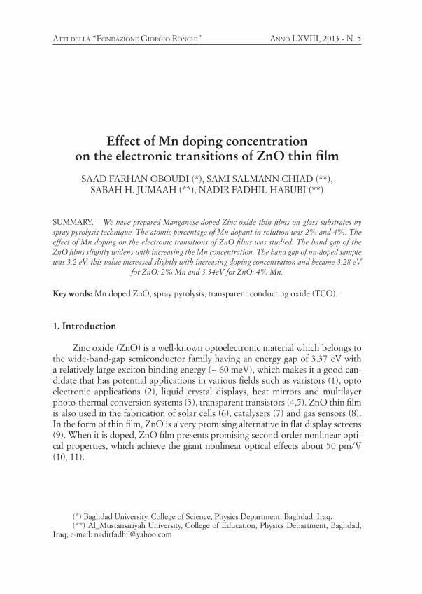
Effect of Mn doping concentration on the electronic transitions of ZnO thin fi lm
SAAD FARHAN OBOUDI (*), SAMI SALMANN CHIAD (**),SABAH H. JUMAAH (**), NADIR FADHIL HABUBI (**)
SUMMARY. – We have prepared Manganese-doped Zinc oxide thin fi lms on glass substrates by spray pyrolysis technique. The atomic percentage of Mn dopant in solution was 2% and 4%. The effect of Mn doping on the electronic transitions of ZnO fi lms was studied. The band gap of the ZnO fi lms slightly widens with increasing the Mn concentration. The band gap of un-doped sample was 3.2 eV, this value increased slightly with increasing doping concentration and became 3.28 eV for ZnO: 2% Mn and 3.34eV for ZnO: 4% Mn.
Key words: Mn doped ZnO, spray pyrolysis, transparent conducting oxide (TCO).
1. Introduction
Zinc oxide (ZnO) is a well-known optoelectronic material which belongs to the wide-band-gap semiconductor family having an energy gap of 3.37 eV with a relatively large exciton binding energy (~ 60 meV), which makes it a good can-didate that has potential applications in various fi elds such as varistors (1), opto electronic applications (2), liquid crystal displays, heat mirrors and multilayer photo-thermal conversion systems (3), transparent transistors (4,5). ZnO thin fi lm is also used in the fabrication of solar cells (6), catalysers (7) and gas sensors (8). In the form of thin fi lm, ZnO is a very promising alternative in fl at display screens (9). When it is doped, ZnO fi lm presents promising second-order nonlinear opti-cal properties, which achieve the giant nonlinear optical effects about 50 pm/V (10, 11).
(*) Baghdad University, College of Science, Physics Department, Baghdad, Iraq.(**) Al_Mustansiriyah University, College of Education, Physics Department, Baghdad,
Iraq; e-mail: [email protected]
ATTI DELLA “FONDAZIONE GIORGIO RONCHI” ANNO LXVIII, 2013 - N. 5
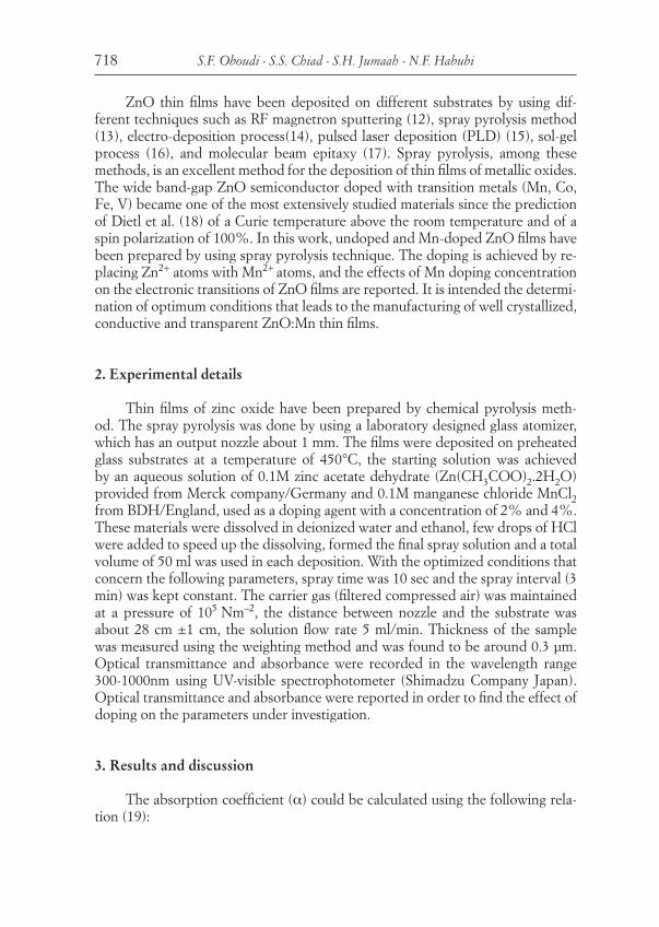
S.F. Oboudi - S.S. Chiad - S.H. Jumaah - N.F. Habubi718
ZnO thin fi lms have been deposited on different substrates by using dif-ferent techniques such as RF magnetron sputtering (12), spray pyrolysis method (13), electro-deposition process(14), pulsed laser deposition (PLD) (15), sol-gel process (16), and molecular beam epitaxy (17). Spray pyrolysis, among these methods, is an excellent method for the deposition of thin fi lms of metallic oxides. The wide band-gap ZnO semiconductor doped with transition metals (Mn, Co, Fe, V) became one of the most extensively studied materials since the prediction of Dietl et al. (18) of a Curie temperature above the room temperature and of a spin polarization of 100%. In this work, undoped and Mn-doped ZnO fi lms have been prepared by using spray pyrolysis technique. The doping is achieved by re-placing Zn2+ atoms with Mn2+ atoms, and the effects of Mn doping concentration on the electronic transitions of ZnO fi lms are reported. It is intended the determi-nation of optimum conditions that leads to the manufacturing of well crystallized, conductive and transparent ZnO:Mn thin fi lms.
2. Experimental details
Thin fi lms of zinc oxide have been prepared by chemical pyrolysis meth-od. The spray pyrolysis was done by using a laboratory designed glass atomizer, which has an output nozzle about 1 mm. The fi lms were deposited on preheated glass substrates at a temperature of 450°C, the starting solution was achieved by an aqueous solution of 0.1M zinc acetate dehydrate (Zn(CH3COO)2.2H2O) provided from Merck company/Germany and 0.1M manganese chloride MnCl2 from BDH/England, used as a doping agent with a concentration of 2% and 4%. These materials were dissolved in deionized water and ethanol, few drops of HCl were added to speed up the dissolving, formed the fi nal spray solution and a total volume of 50 ml was used in each deposition. With the optimized conditions that concern the following parameters, spray time was 10 sec and the spray interval (3 min) was kept constant. The carrier gas (fi ltered compressed air) was maintained at a pressure of 105 Nm–2, the distance between nozzle and the substrate was about 28 cm ±1 cm, the solution fl ow rate 5 ml/min. Thickness of the sample was measured using the weighting method and was found to be around 0.3 µm. Optical transmittance and absorbance were recorded in the wavelength range 300-1000nm using UV-visible spectrophotometer (Shimadzu Company Japan). Optical transmittance and absorbance were reported in order to fi nd the effect of doping on the parameters under investigation.
3. Results and discussion
The absorption coeffi cient (α) could be calculated using the following rela-tion (19):
Effect of Mn doping concentration … 719
[1]
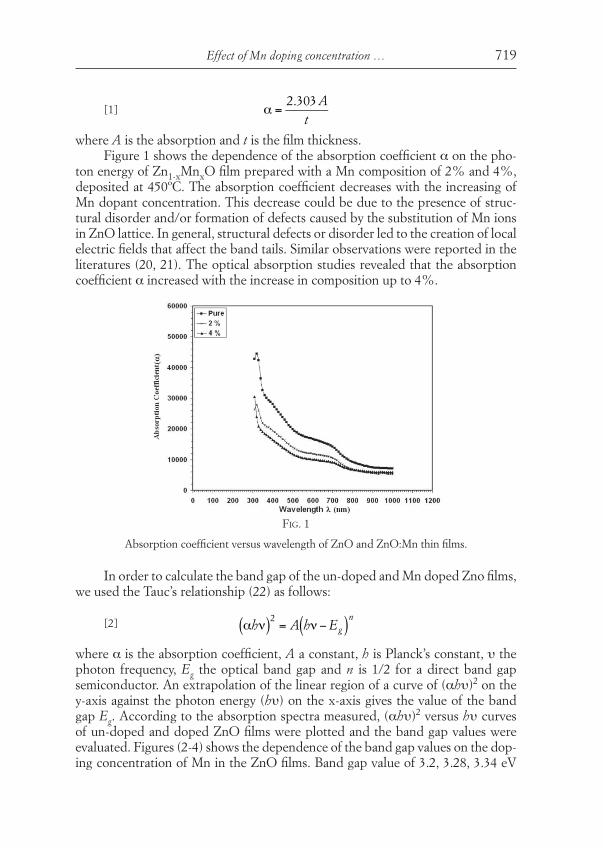
where A is the absorption and t is the fi lm thickness.Figure 1 shows the dependence of the absorption coeffi cient α on the pho-
ton energy of Zn1-xMnxO fi lm prepared with a Mn composition of 2% and 4%, deposited at 450ºC. The absorption coeffi cient decreases with the increasing of Mn dopant concentration. This decrease could be due to the presence of struc-tural disorder and/or formation of defects caused by the substitution of Mn ions in ZnO lattice. In general, structural defects or disorder led to the creation of local electric fi elds that affect the band tails. Similar observations were reported in the literatures (20, 21). The optical absorption studies revealed that the absorption coeffi cient α increased with the increase in composition up to 4%.
α =
2.303 At
FIG. 1
Absorption coeffi cient versus wavelength of ZnO and ZnO:Mn thin fi lms.
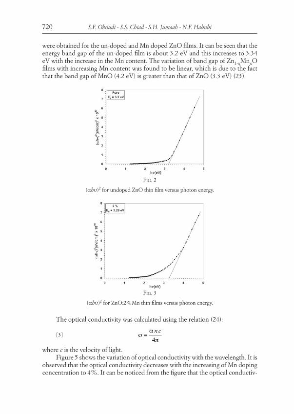
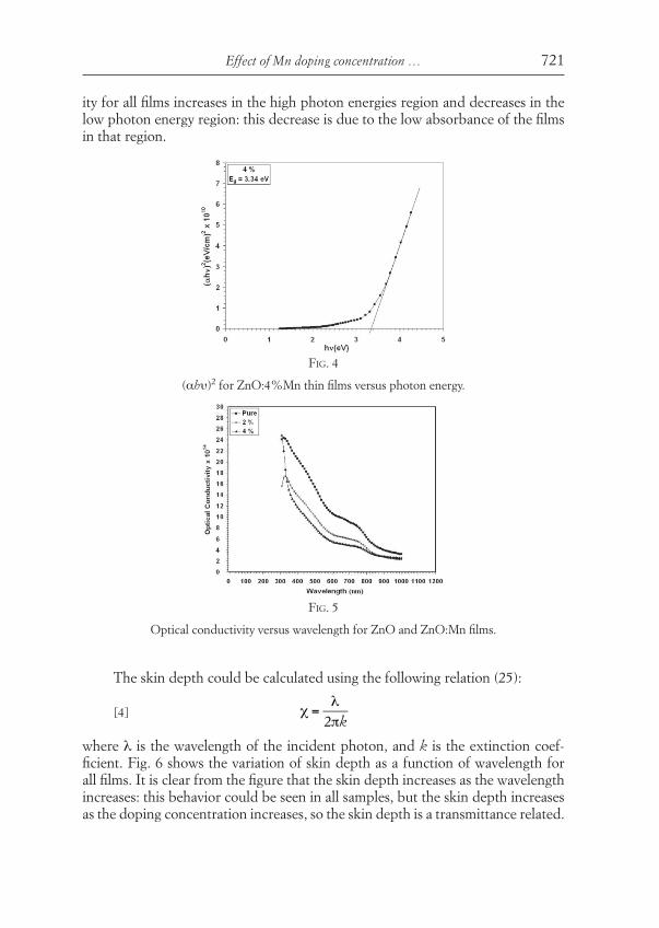
In order to calculate the band gap of the un-doped and Mn doped Zno fi lms, we used the Tauc’s relationship (22) as follows:
[2]
where α is the absorption coeffi cient, A a constant, h is Planck’s constant, υ the photon frequency, Eg the optical band gap and n is 1/2 for a direct band gap semiconductor. An extrapolation of the linear region of a curve of (αhυ)2 on the y-axis against the photon energy (hυ) on the x-axis gives the value of the band gap Eg. According to the absorption spectra measured, (αhυ)2 versus hυ curves of un-doped and doped ZnO fi lms were plotted and the band gap values were evaluated. Figures (2-4) shows the dependence of the band gap values on the dop-ing concentration of Mn in the ZnO fi lms. Band gap value of 3.2, 3.28, 3.34 eV
αhν( )2
= A hν −Eg( )n
S.F. Oboudi - S.S. Chiad - S.H. Jumaah - N.F. Habubi720
were obtained for the un-doped and Mn doped ZnO fi lms. It can be seen that the energy band gap of the un-doped fi lm is about 3.2 eV and this increases to 3.34 eV with the increase in the Mn content. The variation of band gap of Zn1-xMnxO fi lms with increasing Mn content was found to be linear, which is due to the fact that the band gap of MnO (4.2 eV) is greater than that of ZnO (3.3 eV) (23).
FIG. 2
(αhυ)2 for undoped ZnO thin fi lm versus photon energy.
FIG. 3
(αhυ)2 for ZnO:2%Mn thin fi lms versus photon energy.
The optical conductivity was calculated using the relation (24):
[3]
where c is the velocity of light.Figure 5 shows the variation of optical conductivity with the wavelength. It is
observed that the optical conductivity decreases with the increasing of Mn doping concentration to 4%. It can be noticed from the fi gure that the optical conductiv-
σ =
αnc4π
Effect of Mn doping concentration … 721
ity for all fi lms increases in the high photon energies region and decreases in the low photon energy region: this decrease is due to the low absorbance of the fi lms in that region.
FIG. 4
(αhυ)2 for ZnO:4%Mn thin fi lms versus photon energy.
FIG. 5
Optical conductivity versus wavelength for ZnO and ZnO:Mn fi lms.
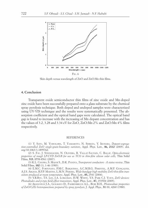
The skin depth could be calculated using the following relation (25):
[4]
where λ is the wavelength of the incident photon, and k is the extinction coef-fi cient. Fig. 6 shows the variation of skin depth as a function of wavelength for all fi lms. It is clear from the fi gure that the skin depth increases as the wavelength increases: this behavior could be seen in all samples, but the skin depth increases as the doping concentration increases, so the skin depth is a transmittance related.
χ =
λ
2πk
S.F. Oboudi - S.S. Chiad - S.H. Jumaah - N.F. Habubi722
4. Conclusion
Transparent oxide semiconductor thin fi lms of zinc oxide and Mn-doped zinc oxide have been successfully prepared onto a glass substrate by the chemical spray pyrolysis technique. Both doped and undoped samples were characterized using UV-VIS technique and the results were systematically presented. The ab-sorption coeffi cient and the optical band gaps were calculated. The optical band gap is found to increase with the increasing of Mn dopant concentration and has the values of 3.2, 3.28 and 3.34 eV for ZnO, ZnO:Mn 2% and ZnO:Mn 4% fi lms respectively.
REFERENCES
(1) Y. SATO, M. YODOGAWA, T. YAMAMOTO, N. SHIBATA, Y. IKUHARA, Dopant-segrega-tion-controlled ZnO single-grain-boundary varistors, Appl. Phys. Lett., 86, 2112 (2005). doi.org/10.1063/1.1899762.
(2) S. FAY, J. STEINHAUSER, N. OLIVEIRA, R. VALLAT-SAUVAIN, C. BALLIF, Opto-electronic properties of rough LP-CVD ZnO:B for use as TCO in thin-fi lm silicon solar cells, Thin Solid Films, 515. 8558-8561 (2007).
(3) K.L. CHOPRA, S. MAJOR S., D.K. PANDYA, Transparent conductors - A status review, Thin Solid Films, 102 (1), 1-46 (1983).
(4) E.M.C. FORTUNATO, P.M.C. BARQUINHA, A.C.M.B.G. PIMENTEL, A.M.F. GONÇALVES, A.J.S. ARQUES, R.F.P. MARTINS, L.M.N. PEREIRA, Wide-bandgap high-mobility ZnO thin-fi lm tran-sistors produced at room temperature, Appl. Phys. Lett., 85, 2541 (2004).
(5) Y.R.RYU, T.S. LEE, J.A. LUBGUBAN, H.W. WHITE, Y.S. PARK C.J. YOUN, ZnO devices: Photodiodes and p-type fi eld-effect transistors, Appl. Phys. Lett., 87, 153504 (2005).
(6) ARANOVICH J.A., GOLMAYO D., FAHRENBRUCH A.L., BUBE R.H., Photovoltaic properties of ZnO/CdTe heterojunctions prepared by spray pyrolysis, J. Appl. Phys., 51 (8), 4260 (1980).
FIG. 6
Skin depth versus wavelength of ZnO and ZnO:Mn thin fi lms.
Effect of Mn doping concentration … 723
(7) M. MIKI-YOSHIDA, V. COLLINS-MARTINEZ, P. AMEZAGA-MADRID, P.A. AGUILAR-ELGUE ZABAL, Thin fi lms of photo catalytic TiO2 and ZnO deposited inside eatubing by Spray pyrolysis, Thin Solid Films, 419, 60-64 (2002).
(8) H.J. LIM, D. YONG, Y.J. OHA, Gas sensing properties of ZnO thin fi lms prepared by micro contact printing, Sensor Actuator, A, 405-410 (2006).
(9) A. GHOSH, S. BASU, Spray/CVD deposition and characterization of surface modifi ed zinc oxide thick fi lms for gas sensor, Mat. Chem. Phys., 27, 45-54 (1991).
(10) J. EBOTHE, I,V. KITYK, S. BENET, B. CLAUDET, K.J. PLUCINSKI, K. OZGA, Photo induced effects in ZnO fi lms deposited on MgO substrates, Opt. Comm., 268, 269-272 (2006).
(11) J. EBOTHE, R. MIEDZINSKI, V. KAPUSTIANYK, B. TURKO, B. KULYK, W. GRUHN, Optical SHG for ZnO fi lms with different morphology stimulated by UV-laser Thermo treatment, J Physic: Conf. Ser., 79, 012001 (2007).
(12) X. PENG, H. ZANG, Z. WANG, J. XU, Y. WANG, Blue-violet luminescence double peak of In-doped fi lms prepared by radio frequency sputtering, J. Luminescence, 128, 328-332 (2008).
(13) B.J. LOKHANDE, M.D. UPLANE, Structural, optical and electrical studies on spray depos-ited highly oriented ZnO fi lms, Appl. Surface Sci., 167 (3-4), 243-246 (2000).
(14) S. ILICAN, M. CAGLAR, Y. CAGLAR, B. DEMIRCI, Polycrystalline indium-doped ZnO thin fi lms: preparation and characterization, J. Opt. and Adv. Mat., 10, 2592-2598 (2008).
(15) H. JAE, T. HITOSHI, K. TOMOJI, Initial preferred growth in zinc oxide thin fi lms on Si and amorphous substrates by a pulsed laser deposition, J. of Crystal Growth, 226 (4), 493-500 (2001).
(16) Y. NATSUME, H. SAKATA, Zinc oxide fi lms prepared by sol-gel spin-coating, Thin Solid Films, 372 (1-2), 30-36 (2000).
(17) D.M. BAGNALL, Y.F. CHEN, Z. ZHU, T. YAO, S. KOYAMA, Y. SHENM, T. GOTO, Optically pumped lasing of ZnO at room temperature, Appl. Phys. Lett., 70 (17), 2230 (1997).
(18) T. DIETL, H. OHNO, F. MATSUKURA, J. CIBERT, D. FERRAND, Zener Model Description of Ferromagnetism in Zinc-Blende Magnetic Semiconductors, Science, 287, 1019-1022 (2000).
(19) X. HAN, R. LIU, W. CHEN, Z. XU, Properties of nanocrystalline zinc oxide thin fi lms prepared by thermal decomposition of electrodeposited zinc peroxide, Thin Solid Films, 516, 4025-4029 (2008).
(20) C. LIU, F. YUN, B. XIAO, S.-J. CHO, Y.T. MOON, H. MORKOC¸, M. ABOUZAID, R. RUTER-ANA, K.M. YU, W. WALUKIEWICZ, Structural analysis of ferromagnetic Mn-doped ZnO thin fi lms deposited by radio frequency magnetron sputtering, J. Appl. Phys., 97, 126107 (2005).
(21) I. AKYUZ, S. KOSE, F. ATAY, V. BILGIN, The optical, structural and morphological proper-ties of ultrasonically sprayed ZnO:Mn fi lms, Semicond. Sci. Technol., 21, 1620 (2006).
(22) J. TAUC, Amorphous and Liquid Semiconductors, (Plenum Press, New York, 1974).(23) J. HUGE, C. CARABATOS, Band structure and opticalproperties of MnO, Solid State
Comm., 60, 369-372 (1986).(24) J.I. PANKOVE, Optical processes in semiconductors, (Dover Publ. Inc.. New York,
1975), p. 91.(25) J.F. ELOY, Power Lasers, (Nat. School of Physics, Grenoble, France: John Wiley and
Sons, 1984), p. 59.
Atti dellA “FondAzione GiorGio ronchi” Anno lXViii, 2013 - n. 5
INDEX
Adaptive opticsK.N. CHOPRA, A short review on modeling and compensation of the aberrations and turbulence effects by adaptive optics technology
BiologyF.H. KAMEL, C.H. SAEED, S.S. QADER, Biological effect of magnetic field on the ultra structure of Staphylococcus aureus
ElectromagnetismD. SCHIAVULLI, A. SORRENTINO, M. MIGLIACCIO, A discussion on the use of X-band SAR images in marine applications
MaterialsZ. AL-RAMADH, H. GHAZI, A. HASHIM, Effect of Carbon NanoFiber on the Transmittance of Poly-Vinyl-Alcohol Edge FiltersM. HADI, S. HADI, A. HASHIM, Study of mechanical properties of UPE-AgNO3 and AlNO3 composites
OphthalmologyA.J. DEL ÁGUILA-CARRASCO, V. SANCHIS-JURADO, A. DOMÍNGUEZVI-CENT, D. MONSÁLVEZ-ROMÍN, P. BERNAL-MOLINA, Importance of pupil size measurement in refractive surgery
Optical instrumentationA.A.D. Al-ZUKY, M. ABDULSTTAR, Using Tilting Angle to Estimate Square Range
Physics of the matterD.H. AL-AMIEDY, Z.A. SALEH, R.K. AL-YASARI, Lambda doubling calculation for Cu63F19
PlasmasK.N. CHOPRA, A short note on the technical investigations of the plasma treatment for biomedical applications
Science of visionL. HSIN HSIN, Visual Cognition: From the Abstract to the Figurative Outline-Con-tinuation-In-Anticipation (OCIA) Phenomena
SpintronicsK.N. CHOPRA, New Materials and their Selection for Designing and Fabricating the Spintronic Devices. A Technical Note
Thin filmsH. SALEH SABIA, N.Z. SHAREEF, The effect of thermal annealing on the electri-cal properties of Ge-Se-Te thin filmsS.S. CHIAD, S.F. OBOUDI, Z.A. TOMA, N.F. HABUBI, Optical dispersion char-acterization of sprayed mixed SnO2-CuO thin filmsB.E. GASGOUS, M.M. ISMAIL, N.I. HASSAN, Effect of laser irradiation on the optical properties of CdO thin filmsG.H. MOHAMED, S.S. CHIAD, S.F. OBOUDI, N.F. HABUBI, Fabrication and characterization of nanoparticles ZnO-NiO thin films prepared by thermal evapora-tion techniqueS.F. OBOUDI, S.S. CHIAD, S.H. JUMAAH, N.F. HABUBI, Effect of Mn doping concentration on the electronic transitions of ZnO thin films
VarietyP. STEFANINI, Il coleottero Lucciola che non vola
Pag. 579
» 595
» 601
» 611
» 615
» 619
» 627
» 637
» 645
» 661
» 673
» 681
» 689
» 699
» 707
» 717
» 725
Related Documents