Effect of fabrication errors in channel waveguide Bragg gratings Giuseppe Coppola, Andrea Irace, Antonello Cutolo, and Mario Iodice The spectral performances of nonideal rectangular Bragg gratings, integrated in a rib waveguide, are analyzed by a multilayer approach based on the effective-index method. The effects of errors on the photolithographic definition of the grating, that is, period and shape, and of errors on the control of etching depth are investigated. Also the influence of the stitching error, which is unavoidable when the grating is realized by means of electron-beam photolithography, is addressed. A novel analytical ap- proach that extends coupled-mode theory to the analysis of real gratings is also presented. © 1999 Optical Society of America OCIS codes: 050.1950, 130.0130. 1. Introduction Semiconductor devices that make extensive use of Bragg’s gratings are commonly used today for differ- ent applications, from distributed Bragg reflector lasers 1–4 to optoelectronic amplitude and phase mod- ulators, 5,6 to realize passive or electrically tunable filters 7,8 and components for telecommunication and optical metrology. The development of this kind of application is in any case closely connected to im- provement in knowledge of the fabrication processes needed to pattern silicon or any other material with dimensions and tolerances that are of the order of tenths of nanometers. Two different technological steps are basically needed to realize a periodic per- turbation on a semiconductor waveguide: photoli- thography and etching. Therefore they are the most important sources of errors and uncertainties in de- termining the geometric properties of the grating. There are several different techniques that are use- ful for defining grating-based devices: deep UV pho- tolithography, 9 holography, 10 and electron-beam lithography. 11–13 The choice between these tech- niques is based on the accuracy that we need for realization of the grating. Recent papers have shown that the electron-beam technique can be con- sidered the most suitable approach for defining the grating: Errors smaller than 0.1% of the period length ~i.e., a few nanometers! have been reported. This is obviously the state of the art in photolitho- graphic processes, whereas, in general, errors as large as 10% of the period length ~i.e., some tens of nanometers! must be considered common. So in this paper we focus only on this kind of lithography. In particular, we analyze Bragg gratings inte- grated in channel waveguides realized by combining electron-beam lithography and optical lithography with silicon-on-insulator substrates, 14 as shown in Fig. 1. Traditional optical lithography can be used to define the waveguide rib stripes, and electron- beam lithography is combined with interferometric alignment systems to write highly coherent grating patterns that can span a length of several millime- ters. The use of an alignment-control system comes from the need to reduce the stitching error. Electron-beam technology is characterized by this type of error, which arises from the limited scanning area of the electron beam, usually 100 mm 3 100 mm, if the electron-beam system is used in a high- resolution mode. Then, if a longer grating is needed, an unavoidable misalignment between two subse- quent sections of the reticule can be present. This fact results in a dimension error on the period corre- sponding to the overlap region between two adjacent scanning areas. Research on this topic 13 has shown that an error of 50 nm can be considered as common whereas use of a control system based on laser inter- G. Coppola, A. Irace, and A. Cutolo are with the Department of Electronic Engineering, University of Naples Federico II, Via Clau- dio 21, 80125 Naples, Italy. The email address for A. Irace is [email protected]. M. Iodice is with the Istituto di Ricerca per l’Elettromagnetismo ed i Componenti Elettronici, Con- siglio Nazionale delle Ricerche, Via Diocleziano 328, 80124 Naples, Italy. Received 25 March 1998; revised manuscript received 21 Sep- tember 1998. 0003-6935y99y091752-07$15.00y0 © 1999 Optical Society of America 1752 APPLIED OPTICS y Vol. 38, No. 9 y 20 March 1999

Welcome message from author
This document is posted to help you gain knowledge. Please leave a comment to let me know what you think about it! Share it to your friends and learn new things together.
Transcript
Effect of fabrication errorsin channel waveguide Bragg gratings
Giuseppe Coppola, Andrea Irace, Antonello Cutolo, and Mario Iodice
The spectral performances of nonideal rectangular Bragg gratings, integrated in a rib waveguide, areanalyzed by a multilayer approach based on the effective-index method. The effects of errors on thephotolithographic definition of the grating, that is, period and shape, and of errors on the control ofetching depth are investigated. Also the influence of the stitching error, which is unavoidable when thegrating is realized by means of electron-beam photolithography, is addressed. A novel analytical ap-proach that extends coupled-mode theory to the analysis of real gratings is also presented. © 1999Optical Society of America
OCIS codes: 050.1950, 130.0130.
1. Introduction
Semiconductor devices that make extensive use ofBragg’s gratings are commonly used today for differ-ent applications, from distributed Bragg reflectorlasers1–4 to optoelectronic amplitude and phase mod-ulators,5,6 to realize passive or electrically tunablefilters7,8 and components for telecommunication andoptical metrology. The development of this kind ofapplication is in any case closely connected to im-provement in knowledge of the fabrication processesneeded to pattern silicon or any other material withdimensions and tolerances that are of the order oftenths of nanometers. Two different technologicalsteps are basically needed to realize a periodic per-turbation on a semiconductor waveguide: photoli-thography and etching. Therefore they are the mostimportant sources of errors and uncertainties in de-termining the geometric properties of the grating.
There are several different techniques that are use-ful for defining grating-based devices: deep UV pho-tolithography,9 holography,10 and electron-beamlithography.11–13 The choice between these tech-
G. Coppola, A. Irace, and A. Cutolo are with the Department ofElectronic Engineering, University of Naples Federico II, Via Clau-dio 21, 80125 Naples, Italy. The email address for A. Irace [email protected]. M. Iodice is with the Istituto diRicerca per l’Elettromagnetismo ed i Componenti Elettronici, Con-siglio Nazionale delle Ricerche, Via Diocleziano 328, 80124 Naples,Italy.
Received 25 March 1998; revised manuscript received 21 Sep-tember 1998.
0003-6935y99y091752-07$15.00y0© 1999 Optical Society of America
1752 APPLIED OPTICS y Vol. 38, No. 9 y 20 March 1999
niques is based on the accuracy that we need forrealization of the grating. Recent papers haveshown that the electron-beam technique can be con-sidered the most suitable approach for defining thegrating: Errors smaller than 0.1% of the periodlength ~i.e., a few nanometers! have been reported.This is obviously the state of the art in photolitho-graphic processes, whereas, in general, errors aslarge as 10% of the period length ~i.e., some tens ofnanometers! must be considered common. So in thispaper we focus only on this kind of lithography.
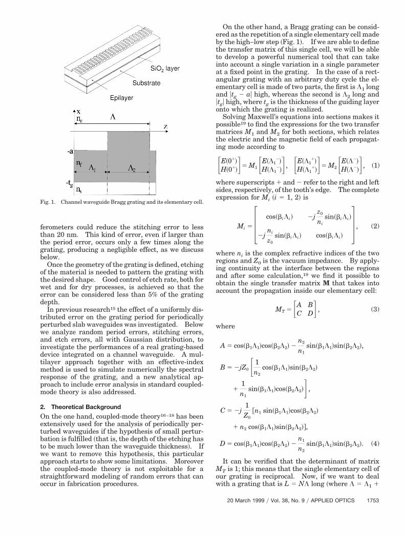
In particular, we analyze Bragg gratings inte-grated in channel waveguides realized by combiningelectron-beam lithography and optical lithographywith silicon-on-insulator substrates,14 as shown inFig. 1. Traditional optical lithography can be usedto define the waveguide rib stripes, and electron-beam lithography is combined with interferometricalignment systems to write highly coherent gratingpatterns that can span a length of several millime-ters. The use of an alignment-control system comesfrom the need to reduce the stitching error.Electron-beam technology is characterized by thistype of error, which arises from the limited scanningarea of the electron beam, usually 100 mm 3 100 mm,if the electron-beam system is used in a high-resolution mode. Then, if a longer grating is needed,an unavoidable misalignment between two subse-quent sections of the reticule can be present. Thisfact results in a dimension error on the period corre-sponding to the overlap region between two adjacentscanning areas. Research on this topic13 has shownthat an error of 50 nm can be considered as commonwhereas use of a control system based on laser inter-
a
ferometers could reduce the stitching error to lessthan 20 nm. This kind of error, even if larger thanthe period error, occurs only a few times along thegrating, producing a negligible effect, as we discussbelow.
Once the geometry of the grating is defined, etchingof the material is needed to pattern the grating withthe desired shape. Good control of etch rate, both forwet and for dry processes, is achieved so that theerror can be considered less than 5% of the gratingdepth.
In previous research15 the effect of a uniformly dis-tributed error on the grating period for periodicallyperturbed slab waveguides was investigated. Belowwe analyze random period errors, stitching errors,and etch errors, all with Gaussian distribution, toinvestigate the performances of a real grating-baseddevice integrated on a channel waveguide. A mul-tilayer approach together with an effective-indexmethod is used to simulate numerically the spectralresponse of the grating, and a new analytical ap-proach to include error analysis in standard coupled-mode theory is also addressed.
2. Theoretical Background
On the one hand, coupled-mode theory16–18 has beenextensively used for the analysis of periodically per-turbed waveguides if the hypothesis of small pertur-bation is fulfilled ~that is, the depth of the etching hasto be much lower than the waveguide thickness!. Ifwe want to remove this hypothesis, this particularapproach starts to show some limitations. Moreoverthe coupled-mode theory is not exploitable for astraightforward modeling of random errors that canoccur in fabrication procedures.
Fig. 1. Channel waveguide Bragg grating and its elementary cell.
On the other hand, a Bragg grating can be consid-ered as the repetition of a single elementary cell madeby the high–low step ~Fig. 1!. If we are able to definethe transfer matrix of this single cell, we will be ableto develop a powerful numerical tool that can takeinto account a single variation in a single parameterat a fixed point in the grating. In the case of a rect-angular grating with an arbitrary duty cycle the el-ementary cell is made of two parts, the first is L1 longand utg 2 au high, whereas the second is L2 long andutgu high, where tg is the thickness of the guiding layeronto which the grating is realized.
Solving Maxwell’s equations into sections makes itpossible19 to find the expressions for the two transfermatrices M1 and M2 for both sections, which relatesthe electric and the magnetic field of each propagat-ing mode according to
FE~01!H~01!G5 M1 FE~L1
2!H~L1
2!G , FE~L11!
H~L11!G5 M2 FE~L2!
H~L2!G , (1)
where superscripts 1 and 2 refer to the right and leftsides, respectively, of the tooth’s edge. The completeexpression for Mi ~i 5 1, 2! is
Mi 5 3 cos~biLi! 2jz0
nisin~biLi!
2jni
z0sin~biLi! cos~biLi! 4 , (2)
where ni is the complex refractive indices of the tworegions and Z0 is the vacuum impedance. By apply-ing continuity at the interface between the regionsand after some calculation,19 we find it possible toobtain the single transfer matrix M that takes intoccount the propagation inside our elementary cell:
MT 5 FA BC DG , (3)
where
A 5 cos~b1L1!cos~b2L2! 2n2
n1sin~b1L1!sin~b2L2!,
B 5 2jZ0 F 1n2
cos~b1L1!sin~b2L2!
11n1
sin~b1L1!cos~b2L2!G ,
C 5 2j1Z0
@n1 sin~b1L1!cos~b2L2!
1 n2 cos~b1L1!sin~b2L2!#,
D 5 cos~b1L1!cos~b2L2! 2n1
n2sin~b1L1!sin~b2L2!. (4)
It can be verified that the determinant of matrixMT is 1; this means that the single elementary cell ofour grating is reciprocal. Now, if we want to dealwith a grating that is L 5 NL long ~where L 5 L1 1
20 March 1999 y Vol. 38, No. 9 y APPLIED OPTICS 1753
cos
wtAgb
tdiwi
ett
t
dt
1
L2!, we can simply evaluate the transfer matrix M ofthe grating:
M 5 )n51
N
MTn 5 FAN BN
CN DNG . (5)
Now we can easily understand how, just by varyingthe parameters inside each matrix MTn in Eq. ~5!, wean take into account all the possible modifications ofur ideal grating. If the grating that we want toimulate is ideal, Eq. ~5! can be rewritten as
M 5 MTn 5 @u1 u2#Fh1
N 00 h2
NG@u1 u2#21, (6)
where hi and ui are, respectively, the eigenvalues andthe eigenvectors of matrix MT. The latter expres-sion can be used to speed up calculations in the anal-ysis of ideal gratings.
From matrix M it is possible with some easy cal-culations to define the transmission coefficient t andthe reflection coefficient r:
r 5
SAN 1no
Z0BND 2
Z0
niSCN 1
no
Z0DND
SAN 1no
Z0BND 1
Z0
niSCN 1
no
Z0DND ,
t 52
SAN 1no
Z0BND 1
Z0
niSCN 1
no
Z0DND . (7)
Then reflectivity and transmissivity are defined as
Teff 5no
niutu2, Reff 5 uru2, (8)
here ni and no are the refractive indices at, respec-ively, the input and the output of the waveguide.ll the results rely only on the fact that the propa-ation along a sequence of slab layers can be modeledy using the transfer matrix approach.Since our scope is to apply this multilayer method
o the study of gratings engraved onto two-imensional waveguides, we apply the effective-ndex method to the transverse cross section of theaveguide and substitute only the modal effective
ndices neff1and neff2
into all the expressions that wehave derived so far. Below we consider single-modechannel waveguides with reference to the fundamen-tal TE propagating mode.
To take into account random errors that occur inthe fabrication of the grating, we need only vary theparameters in the definition of the matrix M; forxample, to introduce a random error in the defini-ion of period L, we can substitute into Eq. ~4! onlyhe real value of each period:
L1R5 L1 1 ε1, L2R
5 L2 1 ε2, (9)
where εi~i 5 1, 2! are the errors that can be commit-ed during fabrication of the grating. In Section 3 a
754 APPLIED OPTICS y Vol. 38, No. 9 y 20 March 1999
etailed description of all the errors that we haveaken into consideration are given.
3. Description of Errors
To determine the propagative behavior of a realstructure, it is necessary to evaluate the statisticaldistribution of fabrication errors and how these er-rors are reflected on the spectral performances of thegrating.
A. Period Error
When going from the ideal layout of a grating to therealization of the real structure, we must consider theposition of the edges of the grating’s steps as affectedby errors due to the nonideal control of the position ofthe electron beam. Therefore the position of eachline scanned by the electron beam is known within anerror that can be assumed to have a Gaussian distri-bution with a zero mean value and a standard devi-ation closely connected to the maximum errorcommitted during the grating definition. Data fromthe literature show that this uncertainty can be con-fined to a value of less than a few tens of nanometersand can be reduced, in the state-of-the-art electron-beam apparatus, to some nanometers. So, for a pe-riod of ;220 nm, we can assume the maximum errorof the tooth size to be smaller than a 10% relativeerror as to the period length itself. We fixed thestandard deviation of the Gaussian random variableso that the probability of having an error larger thanthe uncertainty discussed above should be very small~,1%!. Moreover we considered the errors commit-ted on the two edges of the same tooth independent ofeach other.
B. Stitching Error
The grating patterns are typically composed of hun-dreds or thousands of grating teeth that can span alength of several millimeters. To write this patternwith electron-beam lithography, we must fracture itinto grating segments one electron-beam field longand write each grating segment in turn. Stitchingerrors at the field boundaries correspond to phaseerrors along the grating that in turn distort the fil-ter’s spectral response. The degree of the distortiondepends on the magnitude of the stitching error.
A thorough analysis13 shows that the stitching er-rors are composed of a systematic part and a stochas-tic part. The systematic errors are caused byimperfect calibration of the writing-field size andyordisplacement. The position of the stage with thewafer holder is continuously measured by a laser-beam interferometer. Owing to the limited resolu-tion of the interferometer and the quantized beamdeflection, the exposed fields shift slightly relative toeach other. This shift is one contribution to the sto-chastic stitching error. Another contribution iscaused by the rotation of the stage as it moves be-tween field exposures. The stitching errors have aGaussian distribution with an approximate meanvalue that corresponds to the value of the systematicerror. As previously affirmed, recent data show that
Tbcrvwgatzf
Table 1. Summary of the Physical Geometric Properties of the
a typical value for the mean is 50 nm, but, when moresophisticated interferometric alignment-control sys-tems are used, it is possible to reduce the stitchingerror to 20 nm. The spread of the distribution isgiven by the stochastic errors, and its standard devi-ation is normally13 smaller than 5 nm.
C. Etching Error
The second step in the grating fabrication is its etch-ing. Control of the etching rate in both wet and drysystems has been greatly increased in past years be-cause of the use of in situ process monitor techniques.
he error in determining the exact etching depth cane reduced to a few nanometers.20 For indirect-ontrol techniques, based on knowledge of the etchingate, the accuracy is poorer and the error can reach aalue of 50 nm. This kind of error can be considered,ith good approximation, uniform across the entirerating length. This fact allows us to simplify thenalysis significantly, as we discuss below. Also forhis error we can fix a Gaussian distribution with aero mean value and a standard deviation that is aunction of the maximum error in the grating etching.
4. Simulation Results
A 500-mm-long grating, integrated into a ribwaveguide, has been chosen for all the simulations.In Table 1 the physical and the geometric propertiesof the grating and the waveguide are resumed. Westress that we are analyzing a rib waveguide insteadof a simple slab. Because of the multislabs matrixapproach it is possible to carry out simulations on atwo-dimensional waveguide. The classic coupled-mode theory can be easily applied to slab structures,but a more general formulation is complicated.Moreover the matrix method permits the simulationof both polarizations TE ~Ref. 21! and TM, even withsome correction,22,23 since the classic method must bespecialized for the TM polarization.24
We started from the simulation of the effect of anerror in determining the period length. This erroraffects independently both edges of the grating’steeth and is taken into the account as a Gaussianprocess whose statistics are discussed in Section 3.A.The analysis was carried out for maximum errors asgreat as 25 nm, which is ;10% of the period length,
Waveguide and Grating
Property Value
Grating length 500 mmGrating depth 1.0 mmGrating period 220 nmGrating duty cycle 0.5Substrate refractive index 1.5Guiding layer refractive index 3.5Superstrate refractive index 1.0Rib waveguide thickness 6.0 mmRib waveguide width 6.0 mmRib waveguide definition etch depth 1.5 mm
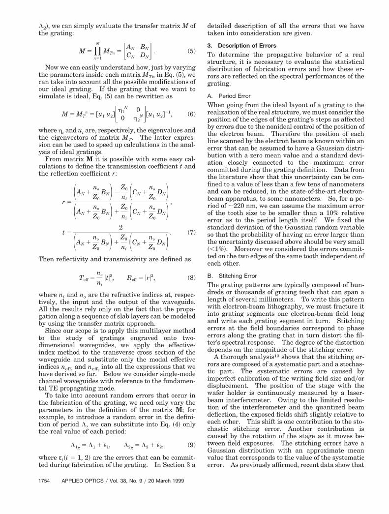
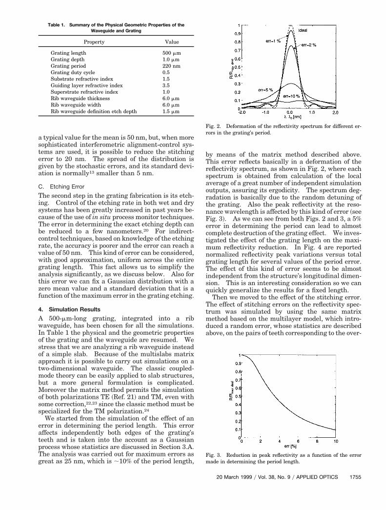
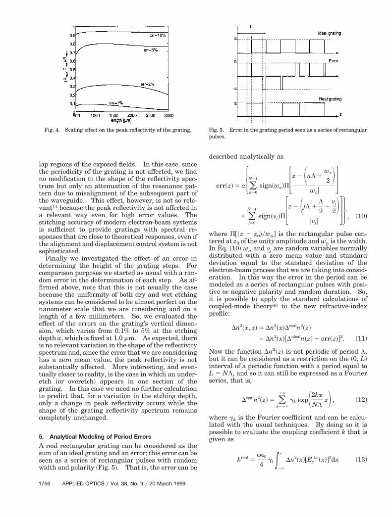
by means of the matrix method described above.This error reflects basically in a deformation of thereflectivity spectrum, as shown in Fig. 2, where eachspectrum is obtained from calculation of the localaverage of a great number of independent simulationoutputs, assuring its ergodicity. The spectrum deg-radation is basically due to the random detuning ofthe grating. Also the peak reflectivity at the reso-nance wavelength is affected by this kind of error ~seeFig. 3!. As we can see from both Figs. 2 and 3, a 5%error in determining the period can lead to almostcomplete destruction of the grating effect. We inves-tigated the effect of the grating length on the maxi-mum reflectivity reduction. In Fig. 4 are reportednormalized reflectivity peak variations versus totalgrating length for several values of the period error.The effect of this kind of error seems to be almostindependent from the structure’s longitudinal dimen-sion. This is an interesting consideration so we canquickly generalize the results for a fixed length.
Then we moved to the effect of the stitching error.The effect of stitching errors on the reflectivity spec-trum was simulated by using the same matrixmethod based on the multilayer model, which intro-duced a random error, whose statistics are describedabove, on the pairs of teeth corresponding to the over-
Fig. 2. Deformation of the reflectivity spectrum for different er-rors in the grating’s period.
Fig. 3. Reduction in peak reflectivity as a function of the errormade in determining the period length.
20 March 1999 y Vol. 38, No. 9 y APPLIED OPTICS 1755
ishste
t
1
lap regions of the exposed fields. In this case, sincethe periodicity of the grating is not affected, we findno modification to the shape of the reflectivity spec-trum but only an attenuation of the resonance pat-tern due to misalignment of the subsequent part ofthe waveguide. This effect, however, is not so rele-vant14 because the peak reflectivity is not affected ina relevant way even for high error values. Thestitching accuracy of modern electron-beam systemsis sufficient to provide gratings with spectral re-sponses that are close to theoretical responses, even ifthe alignment and displacement control system is notsophisticated.
Finally we investigated the effect of an error indetermining the height of the grating steps. Forcomparison purposes we started as usual with a ran-dom error in the determination of each step. As af-firmed above, note that this is not usually the casebecause the uniformity of both dry and wet etchingsystems can be considered to be almost perfect on thenanometer scale that we are considering and on alength of a few millimeters. So, we evaluated theeffect of the errors on the grating’s vertical dimen-sion, which varies from 0.1% to 5% at the etchingdepth a, which is fixed at 1.0 mm. As expected, theres no relevant variation in the shape of the reflectivitypectrum and, since the error that we are consideringas a zero mean value, the peak reflectivity is notubstantially affected. More interesting, and even-ually closer to reality, is the case in which an under-tch ~or overetch! appears in one section of the
grating. In this case we need no further calculationto predict that, for a variation in the etching depth,only a change in peak reflectivity occurs while theshape of the grating reflectivity spectrum remainscompletely unchanged.
5. Analytical Modeling of Period Errors
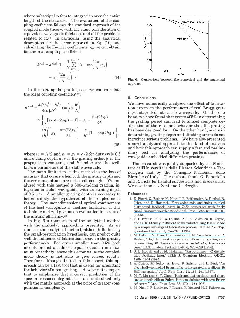
A real rectangular grating can be considered as thesum of an ideal grating and an error; this error can beseen as a series of rectangular pulses with randomwidth and polarity ~Fig. 5!. That is, the error can be
Fig. 4. Scaling effect on the peak reflectivity of the grating.
756 APPLIED OPTICS y Vol. 38, No. 9 y 20 March 1999
described analytically as
err~z! 5 a5(n50
N21
sign~wn!P3z 2 SnL 1wn
2 Duwnu
41 (
j50
N21
sign~nj!P3z 2 SjL 1L
22
nj
2Dunj u
46 , (10)
where P@~z 2 z0!ywn# is the rectangular pulse cen-ered at z0 of the unity amplitude and wn is the width.
In Eq. ~10! wn and nj are random variables normallydistributed with a zero mean value and standarddeviation equal to the standard deviation of theelectron-beam process that we are taking into consid-eration. In this way the error in the period can bemodeled as a series of rectangular pulses with posi-tive or negative polarity and random duration. So,it is possible to apply the standard calculations ofcoupled-mode theory16 to the new refractive-indexprofile:
Dn2~x, z! 5 Dn2~x!Drealn2~z!
5 Dn2~x!@Didealn~z! 1 err~z!#2. (11)
Now the function Dn2~z! is not periodic of period L,but it can be considered as a restriction on the ~0, L!interval of a periodic function with a period equal toL 5 NL, and so it can still be expressed as a Fourierseries, that is,
Drealn2~z! 5 (k52`
1`
gk expS2kp
NLzD , (12)
where gk is the Fourier coefficient and can be calcu-lated with the usual techniques. By doing so it ispossible to evaluate the coupling coefficient k that isgiven as
kreal 5ve0
4gl *
2`
`
Dn2~x!@Ey~s!~x!#2dx (13)
Fig. 5. Error in the grating period seen as a series of rectangularpulses.
w
where subscript l refers to integration over the entirelength of the structure. The evaluation of the cou-pling coefficient follows the standard approach of thecoupled-mode theory, with the same consideration ofequivalent waveguide thickness and all the problemsrelated to it.25 In particular, using the analyticaldescription for the error reported in Eq. ~10! andcalculating the Fourier coefficients gk, we can obtainfor the real coupling coefficient
kreal 5 kidealH1 21N (
n50
N21 F2 2 cosS2p
LwnD
2 cosS2p
LnnDGJ . (14)
In the rectangular-grating case we can calculatethe ideal coupling coefficient25:
kideal 5k0
2~nc2 2 nf
2!
4prbN2 sinSrpwLD
3 H1q
@exp(22qg2! 2 1# 2 g1 2sin~2hg1!
2h
2 SqhD
2Fg1 2sin~2hg1!
2h G 2qh2 @1 2 cos~2hg1!#J ,
(15)
here w 5 Ly2 and g1 5 g2 5 ay2 for duty cycle 0.5and etching depth a, r is the grating order, b is thepropagation constant, and h and q are the well-known parameters of the slab waveguide.
The main limitation of this method is the loss ofaccuracy that occurs when both the grating depth andthe error magnitude are not small enough. We an-alyzed with this method a 500-mm-long grating, in-tegrated in a slab waveguide, with an etching depthof 0.5 mm. A smaller grating depth is necessary tobetter satisfy the hypotheses of the coupled-modetheory. The monodimensional optical confinementof the host waveguide is another limitation of thistechnique and will give us an evaluation in excess ofthe grating efficiency.26
In Fig. 6 a comparison of the analytical methodwith the multislab approach is presented. As wecan see, the analytical method, although limited bythe small-perturbation hypothesis, can predict quitewell the influence of fabrication errors on the gratingperformances. For errors smaller than 0.5% bothmodels predict an almost equal reduction in maxi-mum reflectivity; above this error value the coupled-mode theory is not able to give correct results.Therefore, although limited in this aspect, this ap-proach can be a fast tool that is useful for predictingthe behavior of a real grating. However, it is impor-tant to emphasize that a correct prediction of thespectral response degradation can be obtained onlywith the matrix approach at the price of greater com-putational complexity.
6. Conclusions
We have numerically analyzed the effect of fabrica-tion errors on the performances of real Bragg grat-ings integrated into a rib waveguide. On the onehand, we have found that errors of 5% in determiningthe grating period can lead to almost complete de-struction of the resonant behavior that the gratinghas been designed for. On the other hand, errors indetermining grating depth and stitching errors do notintroduce serious problems. We have also presenteda novel analytical approach to this kind of analysisand how this approach can supply a fast and prelim-inary tool for analyzing the performances ofwaveguide-embedded diffraction gratings.
This research was jointly supported by the Minis-tero dell’Universita’ e della Ricerca Scientifica e Tec-nologica and by the Consiglio Nazionale delleRicerche of Italy. The authors thank G. Panarielloand R. Fiola for helpful suggestions and discussions.We also thank L. Zeni and G. Breglio.
References1. D. Eisert, G. Bacher, N. Mais, J. P. Reithmaier, A. Forchel, B.
Jobst, and D. Hommel, “First order gain and index coupleddistributed feedback lasers in ZnSe structures with finelytuned emission wavelengths,” Appl. Phys. Lett. 68, 599–601~1996!.
2. T. F. Krauss, R. M. De La Rue, P. J. R. Laybourn, B. Vogele,and C. R. Stanley, “Efficient semiconductor ring lasers madeby a simple self-aligned fabrication process,” IEEE J. Sel. Top.Quantum Electron. 1, 757–760 ~1995!.
3. M. Fallahi, M. Dion, F. Chatenoud, I. M. Temoleton, and R.Barber, “High temperature operation of circular grating sur-face emitting DBR lasers fabricated on an InGaAsyGaAs struc-ture,” IEEE Photon. Technol. Lett. 6, 326–329 ~1994!.
4. S. L. McCall and P. M. Platzman, “An optimized py2 distrib-uted feedback laser,” IEEE J. Quantum Electron. QE-21,1899–1904 ~1985!.
5. A. Cutolo, M. Iodice, A. Irace, P. Spirito, and L. Zeni, “Anelectrically controlled Bragg reflector integrated in a silicon ribSOI waveguide,” Appl. Phys. Lett. 71, 199–201 ~1997!.
6. M. Y. Liu and S. Y. Chou, “High modulation depth and shortcavity length silicon Fabry–Perot modulator with two Braggreflectors,” Appl. Phys. Lett. 68, 170–172 ~1996!.
7. M. Okai, I. F. Lealman, J. Rivers, C. Dix, and M. J. Robertson,
Fig. 6. Comparison between the numerical and the analyticalapproach.
20 March 1999 y Vol. 38, No. 9 y APPLIED OPTICS 1757
“In line Fabry–Perot optical waveguide filter with quasi- gated waveguides with rectangular tooth shape,” IEEE J.
1
chirped grating,” Electron. Lett. 32, 108–109 ~1996!.8. H. J. Lee, N. A. Olsson, H. Henry, R. F. Kazarinov, and K. J.
Orlowski, “Narrowband Bragg reflector filter at 1.52 mm,”Appl. Opt. 27, 211–213 ~1988!.
9. J. Martin and F. Ouellette, “Novel writing technique of longhighly reflective in-fiber gratings,” Electron. Lett. 30, 811–812~1994!.
10. C. H. Lin, Z. H. Zhu, and Y. H. Lo, “New grating fabricationtechnology for optoelectronic devices: cascaded self-inducedholography,” Appl. Phys. Lett. 67, 3072–3074 ~1995!.
11. P. Unger, V. Boegli, P. Buchmann, and R. Germann, “Highresolution electron-beam lithography for fabricating visiblesemiconductor lasers with curved mirrors and integrated ho-lograms,” Microelectron. Eng. 23, 461–464 ~1994!.
12. T. Kjellberg, S. Nilsson, T. Klinga, B. Broberg, and R. Schatz,“Investigation on the spectral characteristics of DFB laserswith different grating configurations made by electron-beamlithography,” J. Lightwave Technol. 11, 1405–1415 ~1993!.
13. T. Kjellberg and R. Schatz, “The effect of stitching errors on thespectral characteristics of DFB lasers fabricated usingelectron-beam lithography,” J. Lightwave Technol. 10, 1256–1266 ~1992!.
14. V. V. Wong, J. Ferrara, J. N. Damask, T. E. Murphy, H. I.Smith, and H. A. Haus, “Distributed Bragg grating integrated-optical filters: synthesis and fabrication,” J. Vac. Sci. Tech-nol. B 13, 2859–2864 ~1995!.
15. A. Basu and J. M. Ballantyne, “Random fluctuations in first-order waveguide grating filters,” Appl. Opt. 18, 2575–2579~1979!.
16. A. Yariv, “Coupled mode theory for guided wave optics,” IEEEJ. Quantum Electron. QE-9, 919–933 ~1973!.
17. A. Hardy, “Exact derivation of coupling coefficients in corru-
758 APPLIED OPTICS y Vol. 38, No. 9 y 20 March 1999
Quantum Electron. QE-20, 1132–1139 ~1984!.18. M. J. Li and S. I. Najafi, “Polarization dependence of grating
assisted waveguide Bragg reflectors,” Appl. Opt. 32, 4517–4521 ~1993!.
19. K. A. Winick, “Effective-index method and coupled theory foralmost-periodic waveguide gratings: a comparison,” Appl.Opt. 31, 757–764 ~1992!.
20. P. Blair, M. R. Taghizadeh, W. Parkers, and C. D. W. Wilkin-son, “High-efficiency binary fan-out gratings by modulation ofhigh-frequency carrier grating,” Appl. Opt. 34, 2406–2413~1995!.
21. P. Verly, R. Tremblay, and J. W. Y. Lit, “Application of theeffective-index method to the study of distributed feedback incorrugated waveguides. TE polarization,” J. Opt. Soc. Am.70, 964–968 ~1980!.
22. P. Verly, R. Tremblay, and J. W. Y. Lit, “Application of theeffective-index method to the study of distributed feedback incorrugated waveguides. TM polarization,” J. Opt. Soc. Am.70, 1218–1221 ~1980!.
23. R. W. Gruhlke and D. G. Hall, “Comparison of two approachesto the waveguide scattering problem: TM polarization,” Appl.Opt. 23, 127–133 ~1984!.
24. W. Streifer, D. R. Scrifres, and R. D. Burnham, “TM-modecoupling coefficients in guided-wave distributed feedback la-sers,” IEEE J. Quantum Electron. QE-12, 74–78 ~1976!.
25. W. Streifer, D. R. Scrifres, and R. D. Burnham, “Couplingcoefficients for distributed feedback single and double hetero-structure diode lasers,” IEEE J. Quantum Electron. QE-11,867–873 ~1975!.
26. G. Weitman and A. Hardy, “Reduction of the coupling coeffi-cients for distributed Bragg reflectors in corrugated narrow ribwaveguide,” IEE Proc. Optoelectron. 144, 101–103 ~1997!.
Related Documents