EEW508 Structure of Surfaces Surface structure Rice terrace

EEW508 Structure of Surfaces Surface structure Rice terrace.
Jan 04, 2016
Welcome message from author
This document is posted to help you gain knowledge. Please leave a comment to let me know what you think about it! Share it to your friends and learn new things together.
Transcript

EEW508Structure of Surfaces
Surface structure
Rice terrace

EEW508Structure of Surfaces
Surface structure revealed by SEM and STM
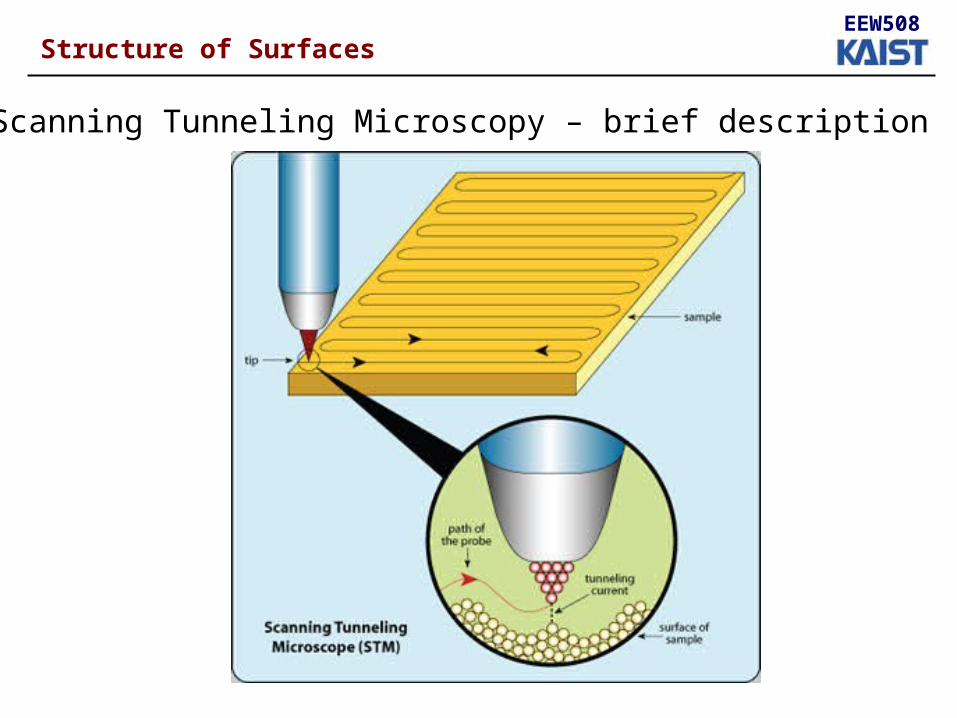
Using STM (Scanning tunneling microscopy) or other techniques such as field ion microscopy (FIM) or LEED (low energy electron diffraction), atomic model of surface structure can be determined.
Surface Chemistryand Catalysis, second editionG. A. Somorjai and Y. Li (2010)

Terrace-step-kink model
EEW508Structure of Surfaces
Steps and kinks are line defects to distinguish them from atomic vacancies or adatoms, which are called point defects.
Relative concentration of atoms in terraces, in line defects, or in point defects can be altered, depending the methods of sample preparation.

EEW508Structure of Surfaces
Terrace – flat surface
Stepped surface
Kinked surface

Dislocations creat surface defects such as steps and kinks
EEW508Structure of Surfaces
Surface Chemistryand Catalysis, second editionG. A. Somorjai and Y. Li (2010)
On heterogeneous solid surface, atoms in terraces are surrounded by the largest number of nearest neighbors. Atoms in steps have fewer, and atoms in kinks have even fewer.
In a rough surface, 10-20% of atoms are often step sites, with about 5% of kink sites.
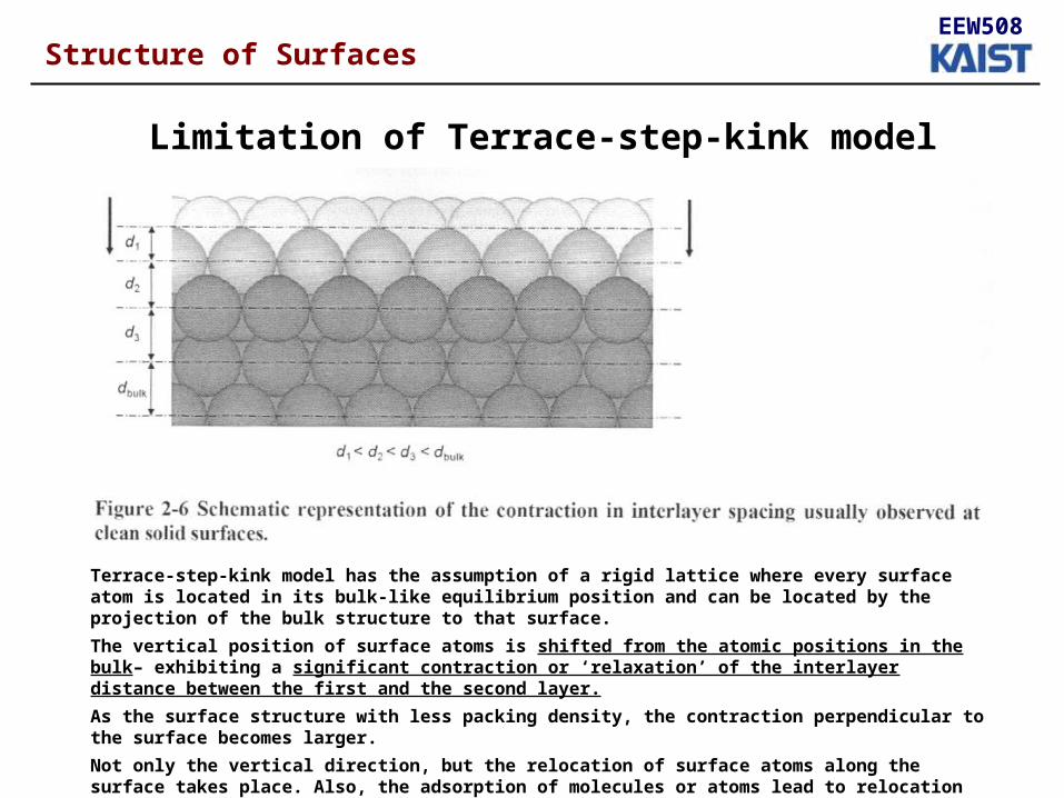
Limitation of Terrace-step-kink model
EEW508Structure of Surfaces
Terrace-step-kink model has the assumption of a rigid lattice where every surface atom is located in its bulk-like equilibrium position and can be located by the projection of the bulk structure to that surface.
The vertical position of surface atoms is shifted from the atomic positions in the bulk– exhibiting a significant contraction or ‘relaxation’ of the interlayer distance between the first and the second layer.
As the surface structure with less packing density, the contraction perpendicular to the surface becomes larger.
Not only the vertical direction, but the relocation of surface atoms along the surface takes place. Also, the adsorption of molecules or atoms lead to relocation of surface atoms to optimize the strength of the adsorption-substrate bond.

Determination of surface structure – Low energy electron diffraction (LEED)
EEW508Structure of Surfaces
LEED produce the quantitative data on bond distance and angles as well as on location of surface atoms and of adsorbed molecules.

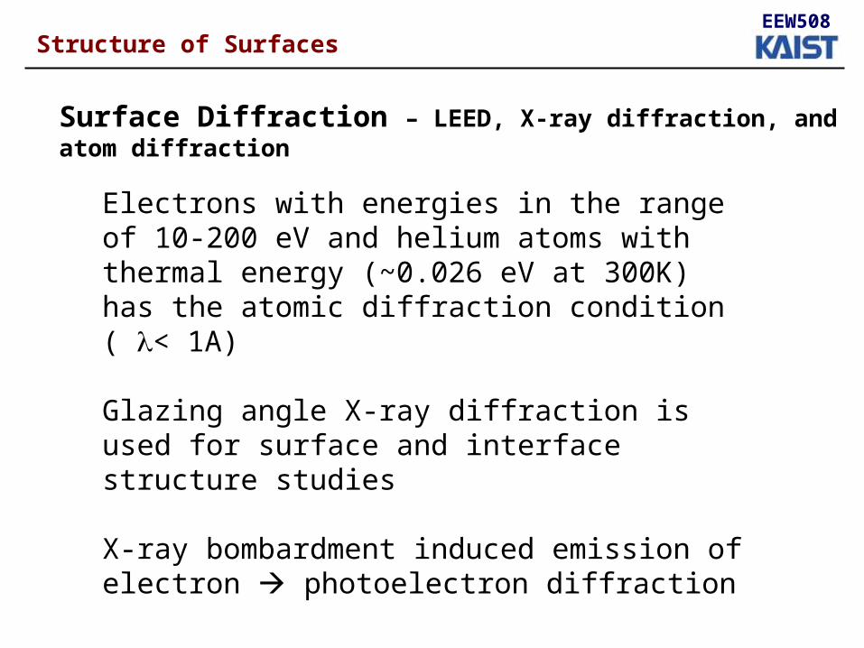
Surface Diffraction – LEED, X-ray diffraction, and atom diffraction
EEW508Structure of Surfaces
The de Broglie wavelength of a particle is given by
mE
h
p
h
2
Where h is Planck’s constant, m is the mass of the particle, and E is the kinetic energy of the particle
For electron, and He atoms
)(
150)(
eVEAo
e )(
02.0)(
eVEAo
He
For X-ray
hchE )(
1024.1)(
4
eVEAo
photon
Surface Diffraction – LEED, X-ray diffraction, and atom diffraction
EEW508Structure of Surfaces
Electrons with energies in the range of 10-200 eV and helium atoms with thermal energy (~0.026 eV at 300K) has the atomic diffraction condition ( < 1A)
Glazing angle X-ray diffraction is used for surface and interface structure studies
X-ray bombardment induced emission of electron photoelectron diffraction

Principle of Low energy electron diffraction (LEED)
EEW508Structure of Surfaces
The single crystal surfaces are used in LEED studies. After chemical or ion-bombardment cleaning in UHV, the crystal is heated to permit the ordering of surface atoms by diffusion to their equilibrium positions.
The electron beam (in the range of 10-200 eV) is backscattered. The elastic electrons that retain their incident kinetic energy are separated from the inelastically scattered electron by applying the reverse potential to the retarding grids. These elastic electrons are accelerated to strike a fluorescent screen and LEED pattern can be obtained.
Types of LEED
Video LEED : LEED patterns can be visualized on a fluorescent screen.
Dynamic LEED or called I-V curve: the intensity I of the diffracted beam is measured as a function of the kinetic energy.

LEED pattern of a Si(100) reconstructed surface. The underlying lattice is a square lattice while the surface reconstruction has a 2x1 periodicity. The diffraction spots are generated by acceleration of elastically scattered electrons onto a hemispherical fluorescent screen. Also seen is the electron gun which generates the primary electron beam. It covers up parts of the screen.
EEW508Structure of Surfaces

EEW508Structure of Surfaces
Example – Si(111)- (7x7)
DAS structure: dimer, adatom, and stacking fault
EEW508Structure of Surfaces
Scanning Tunneling Microscopy – brief description

EEW508Structure of Surfaces
Example – Si(111)- (7x7)
Gerd Binnig and Heinrich Rohrer Nobel prize in Physics (1986)

If the surface unit-cell vector and that are different from and obtained from the bulk projection, then the surface unit vector can be related to the bulk unit vectors
'a
'b
a
b
bmamb
bmama
2221
1211
'
'
mij defines a matrix
2221
1211
mm
mmM
On unreconstructed surface
10
01M
EEW508Structure of Surfaces


Unreconstructed surface of the face-centered crystal structure
EEW508Structure of Surfaces

Unreconstructed surface of the body-centered crystal structure
EEW508Structure of Surfaces

Unreconstructed surface of the diamond crystal structure
EEW508Structure of Surfaces

EEW508Structure of Surfaces
For example, fcc (100) – (2x2)

EEW508Structure of Surfaces
20
02MFor example, fcc (111) – (2x2)

EEW508Structure of Surfaces
20
02MFor example, fcc (110) – (2x2)

EEW508Structure of Surfaces
Abbreviated and Matrix Notation for a variety of superlattices

EEW508Structure of Surfaces
Abbreviated and Matrix Notation for a variety of superlattices

EEW508Structure of Surfaces
Notation of High-Miller-Index Stepped Surface
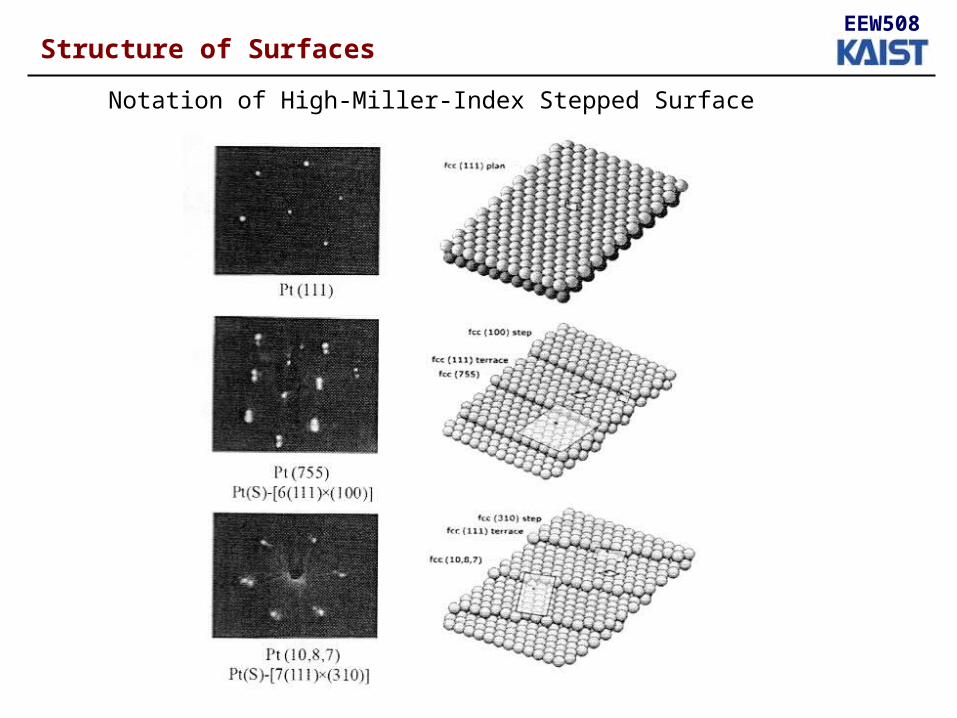
EEW508Structure of Surfaces
Notation of High-Miller-Index Stepped Surface

EEW508Structure of Surfaces
Notation of High-Miller-Index Stepped Surface
stepped surface
kinked surface
6(111) x (100) 4(111) x (100)

EEW508Structure of Surfaces
Bond-Length Contraction or Relaxation
close-packed less close-packed
Related Documents