BUILDING BLOCKS OF INTEGRATED - CIRCUIT AMPLIFIERS Sedra/Smith CHAPTER 7

Eel305 building blocks of op am ps
Jul 16, 2015
Welcome message from author
This document is posted to help you gain knowledge. Please leave a comment to let me know what you think about it! Share it to your friends and learn new things together.
Transcript

BUILDING BLOCKS OFINTEGRATED-CIRCUIT
AMPLIFIERS
Sedra/Smith CHAPTER
7

Integrated-circuit fabrication technology
imposes constraints on—and provides opportunities to—the circuit designer.
While chip-area considerations dictate that
large- and even moderate-value resistors are to be avoided,
constant-current sources are readily available.
Large capacitors, for signal coupling and bypass, are not available to be used,
except perhaps as components external to the IC chip. Even then, the number
of such capacitors has to be kept to a minimum; otherwise the number of chip
terminals increases, and hence the cost.
Very small capacitors, in the picofarad and fraction-of-a-picofarad range,
however, are easy to fabricate in IC MOS technology and can be combined
with MOS amplifiers and MOS switches to realize a wide range of signal
processing functions, both analog and digital.
2
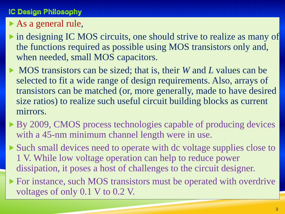
As a general rule,
in designing IC MOS circuits, one should strive to realize as many ofthe functions required as possible using MOS transistors only and, when needed, small MOS capacitors.
MOS transistors can be sized; that is, their W and L values can be selected to fit a wide range of design requirements. Also, arrays of transistors can be matched (or, more generally, made to have desired size ratios) to realize such useful circuit building blocks as current mirrors.
By 2009, CMOS process technologies capable of producing devices with a 45-nm minimum channel length were in use.
Such small devices need to operate with dc voltage supplies close to 1 V. While low voltage operation can help to reduce power dissipation, it poses a host of challenges to the circuit designer.
For instance, such MOS transistors must be operated with overdrive voltages of only 0.1 V to 0.2 V.
3

CMOS is currently the most widely used IC technology for
both analog and digital as well as combined analog and digital
(or mixed-signal) applications.
Nevertheless, bipolar integrated circuits still offer many
exciting opportunities to the analog design engineer.
This is especially the case for general-purpose circuit packages,
such as high-quality op amps that are intended for assembly on
printed-circuit (pc) boards (as opposed to being part of a
system-on-chip). As well, bipolar circuits can provide much
higher output currents and are favored for certain applications,
such as in the automotive industry, for their high reliability
under severe environmental conditions.
Finally, bipolar circuits can be combined with CMOS in innovative
and exciting ways in what is known as BiCMOS technology.
4

The basic gain cell in an IC amplifier is a common-source (CS) or
common-emitter (CE) transistor loaded with a constant-current source, as
shown in Fig. 7.1(a) and (b). These circuits are similar to the CS and CE
amplifiers, except that here we have replaced the resistances RD and RC
with constant-current sources. This is done for two reasons:
First, it is difficult in IC technology to implement resistances with
reasonably precise values; rather, it is much easier to use current sources,
which are implemented using transistors, as we shall see shortly.
Second, by using a constant current source we are in effect operating the
CS and CE amplifiers with a very high (ideally infinite) load resistance;
thus we can obtain a much higher gain than if a finite RD or RC is used.
The circuits in Fig. 7.1(a) and (b) are said to be current-source loaded or
active loaded.
5
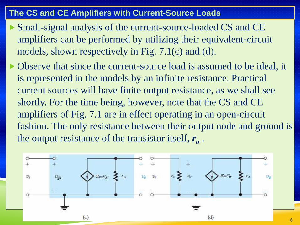
Small-signal analysis of the current-source-loaded CS and CE
amplifiers can be performed by utilizing their equivalent-circuit
models, shown respectively in Fig. 7.1(c) and (d).
Observe that since the current-source load is assumed to be ideal, it
is represented in the models by an infinite resistance. Practical
current sources will have finite output resistance, as we shall see
shortly. For the time being, however, note that the CS and CE
amplifiers of Fig. 7.1 are in effect operating in an open-circuit
fashion. The only resistance between their output node and ground is
the output resistance of the transistor itself, ro .
6
The CS and CE Amplifiers with Current-Source Loads
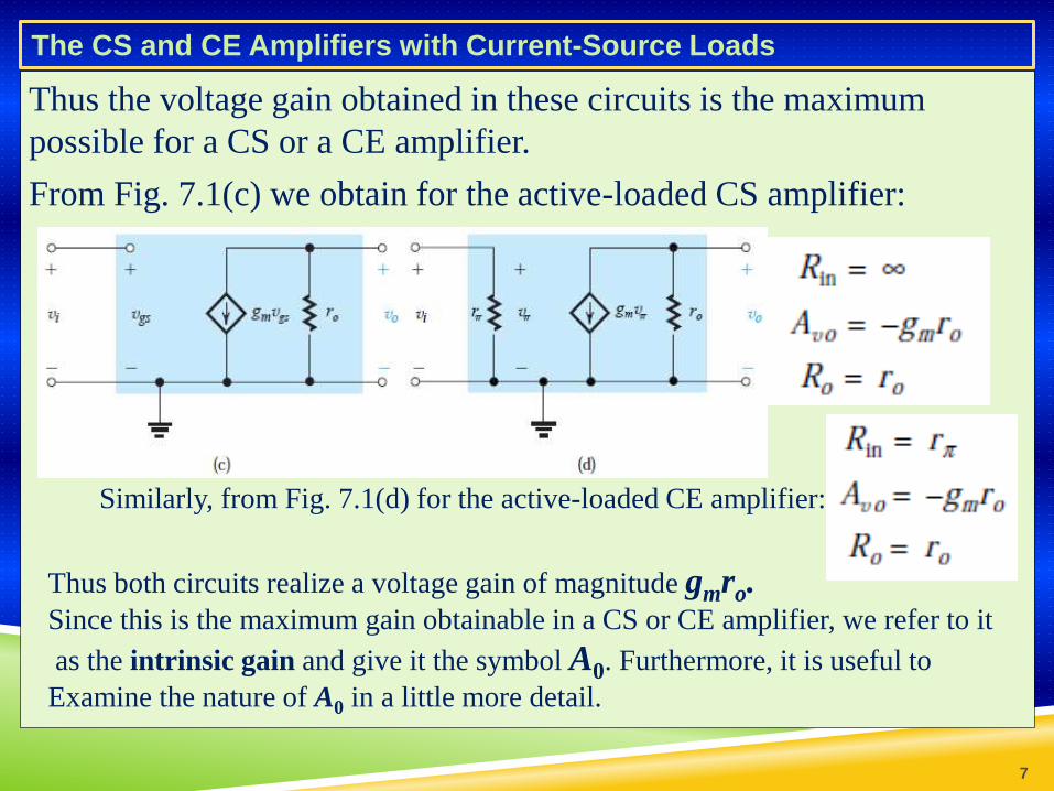
Thus the voltage gain obtained in these circuits is the maximum
possible for a CS or a CE amplifier.
From Fig. 7.1(c) we obtain for the active-loaded CS amplifier:
7
The CS and CE Amplifiers with Current-Source Loads
Similarly, from Fig. 7.1(d) for the active-loaded CE amplifier:
Thus both circuits realize a voltage gain of magnitude gmro.Since this is the maximum gain obtainable in a CS or CE amplifier, we refer to it
as the intrinsic gain and give it the symbol A0. Furthermore, it is useful to
Examine the nature of A0 in a little more detail.
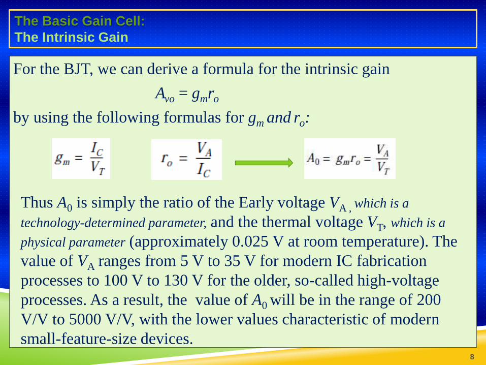
For the BJT, we can derive a formula for the intrinsic gain
Avo = gmro
by using the following formulas for gm and ro:
8
The Basic Gain Cell:
The Intrinsic Gain
Thus A0 is simply the ratio of the Early voltage VA , which is a
technology-determined parameter, and the thermal voltage VT, which is a
physical parameter (approximately 0.025 V at room temperature). The
value of VA ranges from 5 V to 35 V for modern IC fabrication
processes to 100 V to 130 V for the older, so-called high-voltage
processes. As a result, the value of A0 will be in the range of 200
V/V to 5000 V/V, with the lower values characteristic of modern
small-feature-size devices.

It is important to note that for a given bipolar-transistor
fabrication process, A0 is independent of the transistor junction area
and of its bias current.
This is not the case for the MOSFET, as we shall now see.
There are three possible expressions for gm: Two of these are
particularly useful for our purposes here:
and
9
The Intrinsic Gain
For the MOSFET ro we have
where VA is the Early
voltage and V’A is the
technology-dependent
component of the
Early voltage.

Utilizing each of the gm expressions together with the expression for ro,
we obtain for A0 (1)
which can be expressed in the alternate forms
and
The expression in Eq. (1) is the one most directly comparable to that of
the BJT (Eq. 7.9).
10
The Intrinsic Gain

11
The Intrinsic Gain
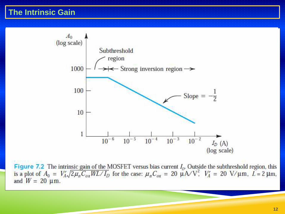
12
The Intrinsic Gain

and
The current-source load of
the CS amplifier in Fig.
7.1(a) can be implemented
using a PMOS transistor
biased in the saturation
region to provide the
required current I, as shown
in Fig. 7.3(a). We can use
the large-signal MOSFET
model (Section 5.2, Fig.
5.15) to model Q2 as shown
in Fig. 7.3(b), where
13
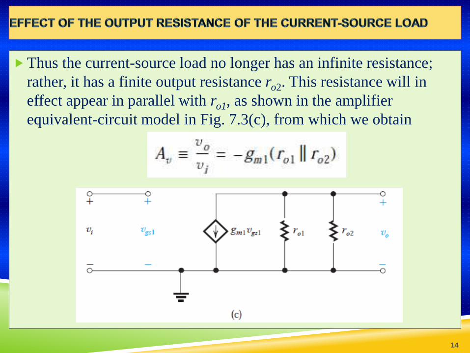
Thus the current-source load no longer has an infinite resistance;
rather, it has a finite output resistance ro2. This resistance will in
effect appear in parallel with ro1, as shown in the amplifier
equivalent-circuit model in Fig. 7.3(c), from which we obtain
14

Thus, not surprisingly, the finite output resistance of the current-
source load reduces the magnitude of the voltage gain from
(gm1ro1) to gm1(ro1||ro2).
This reduction can be substantial.
For instance, if Q2 has an Early voltage equal to that of Q1,
ro2 = ro1
and the gain is reduced by half,
We conclude this section by considering a question:
How can we increase the voltage gain obtained from the basic gain
cell?
15
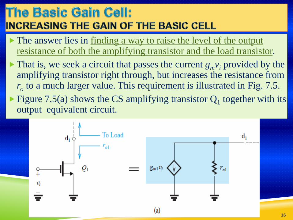
The answer lies in finding a way to raise the level of the output resistance of both the amplifying transistor and the load transistor.
That is, we seek a circuit that passes the current gmvi provided by the amplifying transistor right through, but increases the resistance fromro to a much larger value. This requirement is illustrated in Fig. 7.5.
Figure 7.5(a) shows the CS amplifying transistor Q1 together with its output equivalent circuit.
16
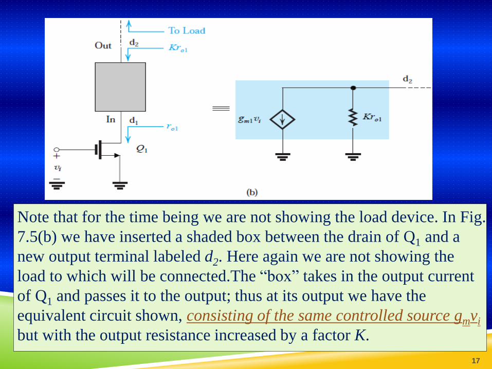
Note that for the time being we are not showing the load device. In Fig.
7.5(b) we have inserted a shaded box between the drain of Q1 and a
new output terminal labeled d2. Here again we are not showing the
load to which will be connected.The “box” takes in the output current
of Q1 and passes it to the output; thus at its output we have the
equivalent circuit shown, consisting of the same controlled source gmvi
but with the output resistance increased by a factor K.
17

Now, what does the box really do?
Since it passes the current but raises the resistance level, it is a current
buffer. It is the dual of the voltage buffer (the source and emitter
followers), which passes the voltage but lowers the resistance level. For
implementing this current-buffering action is the common-gate (or
common-base in bipolar) amplifier.
Indeed, recall that the CG and CB circuits have a unity current gain. What
we have not yet investigated, however, is their resistance transformation
property. Two important final comments:
1. It is not sufficient to raise the output resistance of the amplifying
transistor only. We also need to raise the output resistance of the current-
source load. Obviously, we can use a current buffer to do this also.
2. Placing a CG (or a CB) circuit on top of the CS (or CE) amplifying
transistor to implement the current-buffering action is called cascoding.
18

Cascoding refers to the use of a transistor connected in the common-gate
(or the common base) configuration to provide current buffering for the
output of a common-source (or a common-emitter) amplifying transistor.
Figure 7.6 illustrates the technique for the MOS case. Here the CS
transistor Q1 is the amplifying transistor and Q2 connected in the CG
configuration with a dc bias voltage VG2 (signal ground) at its gate, is the
cascode transistor. The equivalent circuit at the output of the cascode
19
amplifier is that shown in
Fig. 7.6. Thus, the cascode
transistor passes the current
gm1vi to the output node
while raising the resistance
level by a factor K. We will
derive an expression for K.

Figure 7.7(a) shows the MOS cascode
amplifier without a load circuit and with the
gate of Q2 connected to signal ground. Thus
this circuit is for the purpose of small-signal
calculations only. Our objective is to
determine the parameters Gm and Ro of the
equivalent circuit shown in Fig. 7.7(b), which
we shall use to represent the output of the
cascode amplifier.
20
(b)
(a)
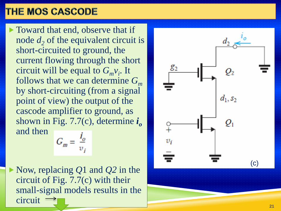
Toward that end, observe that if node d2 of the equivalent circuit is short-circuited to ground, the current flowing through the short circuit will be equal to Gmvi. It follows that we can determine Gm
by short-circuiting (from a signal point of view) the output of the cascode amplifier to ground, as shown in Fig. 7.7(c), determine ioand then
Now, replacing Q1 and Q2 in the circuit of Fig. 7.7(c) with their small-signal models results in the circuit
21
(c)
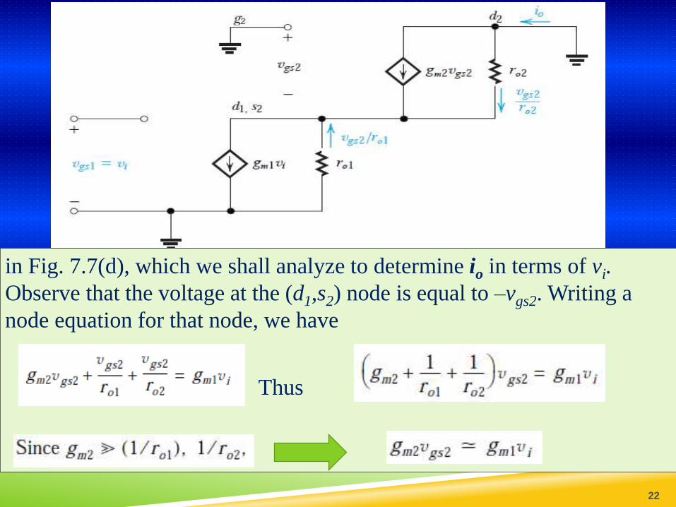
in Fig. 7.7(d), which we shall analyze to determine io in terms of vi.
Observe that the voltage at the (d1,s2) node is equal to –vgs2. Writing a
node equation for that node, we have
Thus
22

In other words, the current of the controlled source of Q1 is equal to
that of the controlled source of Q2. Next, we write an equation for
the d2 node,
Thus
Using
Thus which is the result we have anticipated.
Next we need to determine Ro which is seen from the output
23
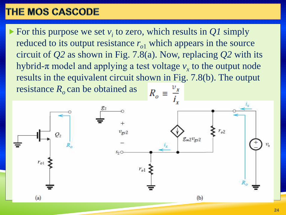
For this purpose we set vi to zero, which results in Q1 simply
reduced to its output resistance ro1 which appears in the source
circuit of Q2 as shown in Fig. 7.8(a). Now, replacing Q2 with its
hybrid-π model and applying a test voltage vx to the output node
results in the equivalent circuit shown in Fig. 7.8(b). The output
resistance Ro can be obtained as
24
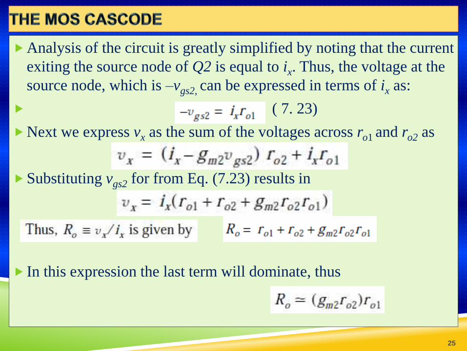
Analysis of the circuit is greatly simplified by noting that the current
exiting the source node of Q2 is equal to ix. Thus, the voltage at the
source node, which is –vgs2, can be expressed in terms of ix as:
( 7. 23)
Next we express vx as the sum of the voltages across ro1 and ro2 as
Substituting vgs2 for from Eq. (7.23) results in
In this expression the last term will dominate, thus
25
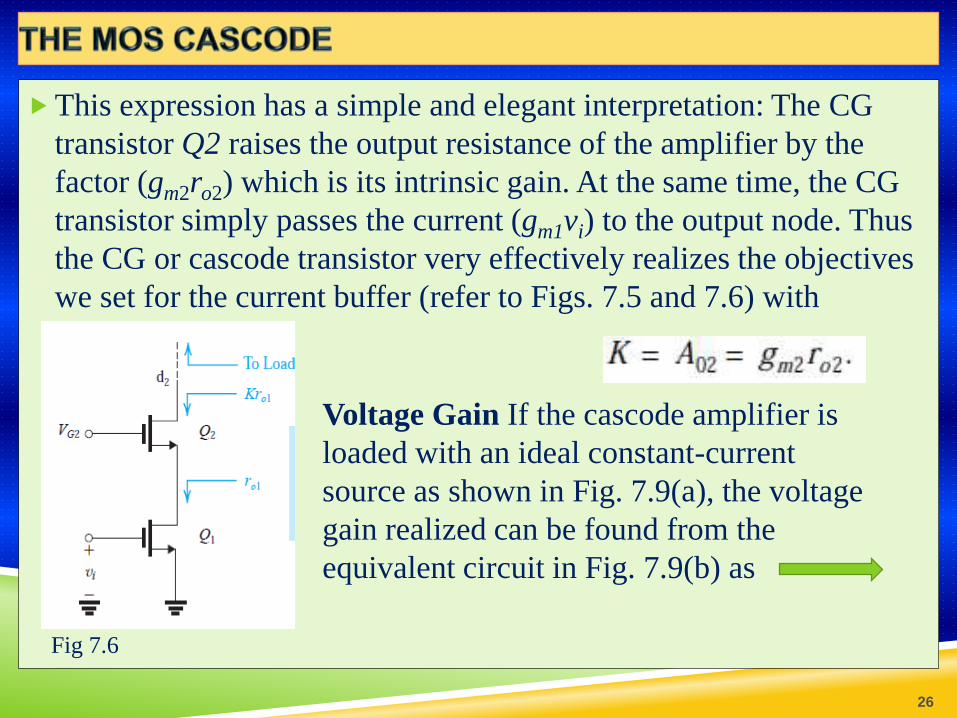
This expression has a simple and elegant interpretation: The CG
transistor Q2 raises the output resistance of the amplifier by the
factor (gm2ro2) which is its intrinsic gain. At the same time, the CG
transistor simply passes the current (gm1vi) to the output node. Thus
the CG or cascode transistor very effectively realizes the objectives
we set for the current buffer (refer to Figs. 7.5 and 7.6) with
26
Fig 7.6
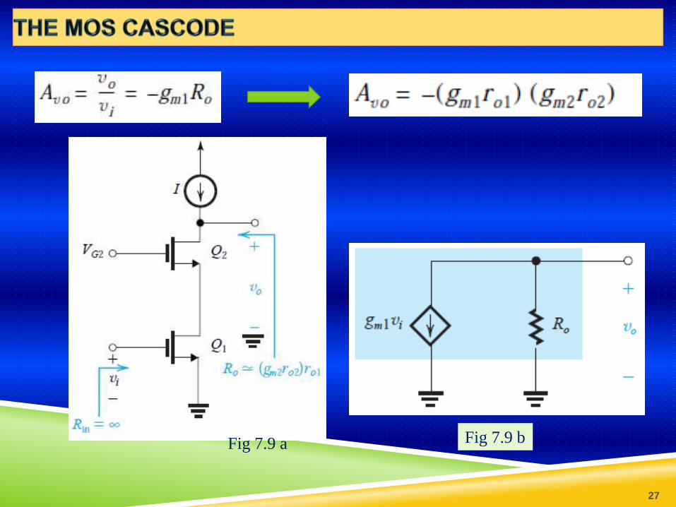
Voltage Gain If the cascode amplifier is
loaded with an ideal constant-current
source as shown in Fig. 7.9(a), the voltage
gain realized can be found from the
equivalent circuit in Fig. 7.9(b) as
27
Fig 7.9 a Fig 7.9 b

Thus cascoding results in increasing the gain
magnitude from A0 to
Cascoding can also be employed to raise
the output resistance of the current-source
load as shown in Fig. 7.10. Here Q4 is the
current-source transistor, and Q3 is the CG
cascode transistor.
Voltages VG3 and VG4 are dc bias voltages.
The cascode transistor Q3 multiplies the
output resistance of Q4, ro4 by (gm3ro3) to
provide an output resistance for the
cascode current source of
28
Fig. 7.10Fig. 7.10
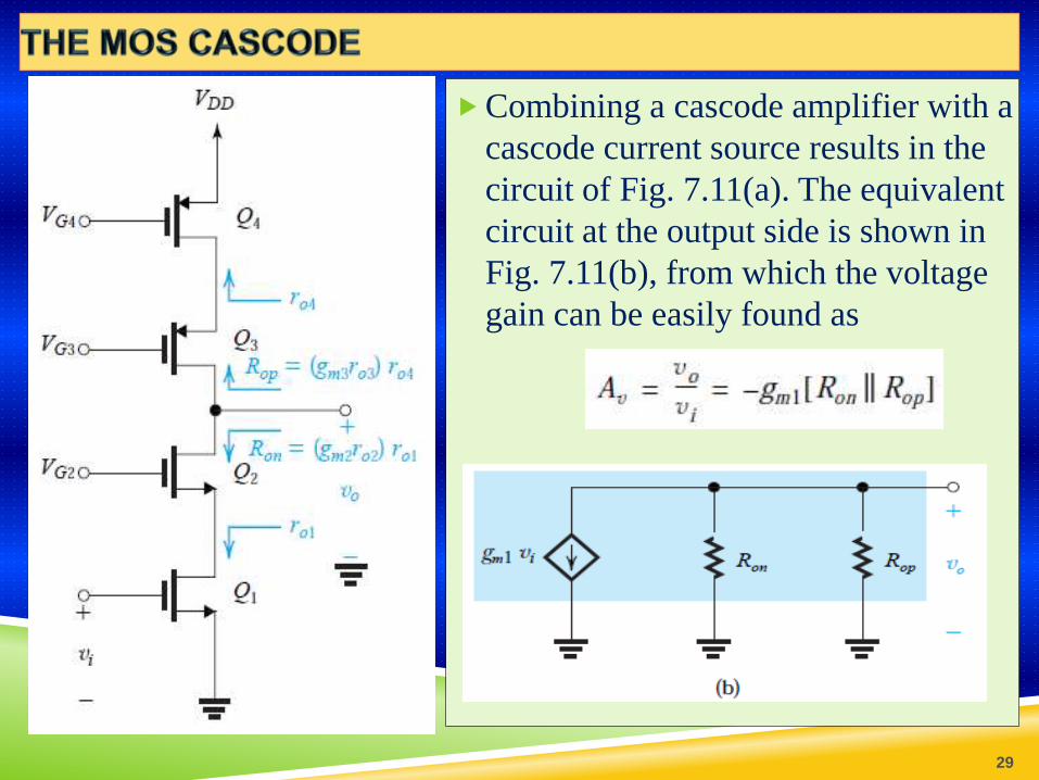
Combining a cascode amplifier with a
cascode current source results in the
circuit of Fig. 7.11(a). The equivalent
circuit at the output side is shown in
Fig. 7.11(b), from which the voltage
gain can be easily found as
29
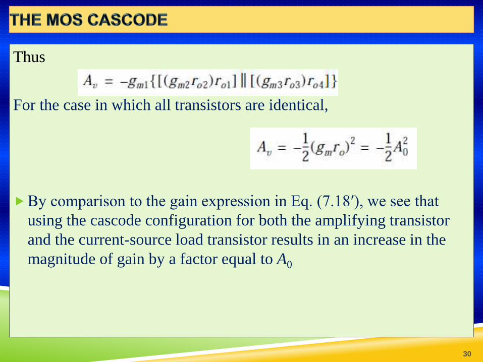
Thus
For the case in which all transistors are identical,
By comparison to the gain expression in Eq. (7.18′), we see that
using the cascode configuration for both the amplifying transistor
and the current-source load transistor results in an increase in the
magnitude of gain by a factor equal to A0
30
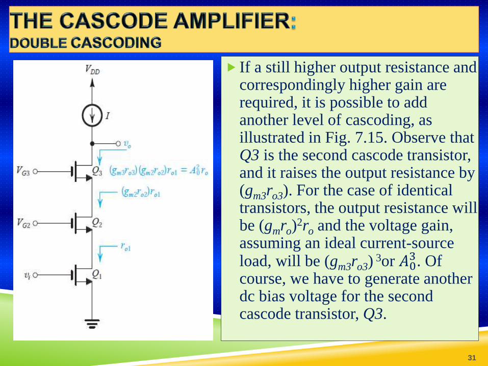
If a still higher output resistance and correspondingly higher gain are required, it is possible to add another level of cascoding, asillustrated in Fig. 7.15. Observe that Q3 is the second cascode transistor, and it raises the output resistance by(gm3ro3). For the case of identicaltransistors, the output resistance will be (gmro)
2ro and the voltage gain, assuming an ideal current-source load, will be (gm3ro3)
3or 𝐴03. Of
course, we have to generate another dc bias voltage for the second cascode transistor, Q3.
31
A drawback of double cascoding is that an additional transistor is
now stacked between the power-supply rails. Furthermore, to realize
the advantage of double cascoding, the current-source load will also
need to use double cascoding with an additional transistor. Since for
proper operation each transistor needs a certain minimum vDS (at
least equal to VOV), and recalling that modern MOS technology
utilizes power supplies in the range of 1V to 2V, we see that there is
a limit on the number of transistors in a cascode stack.
32
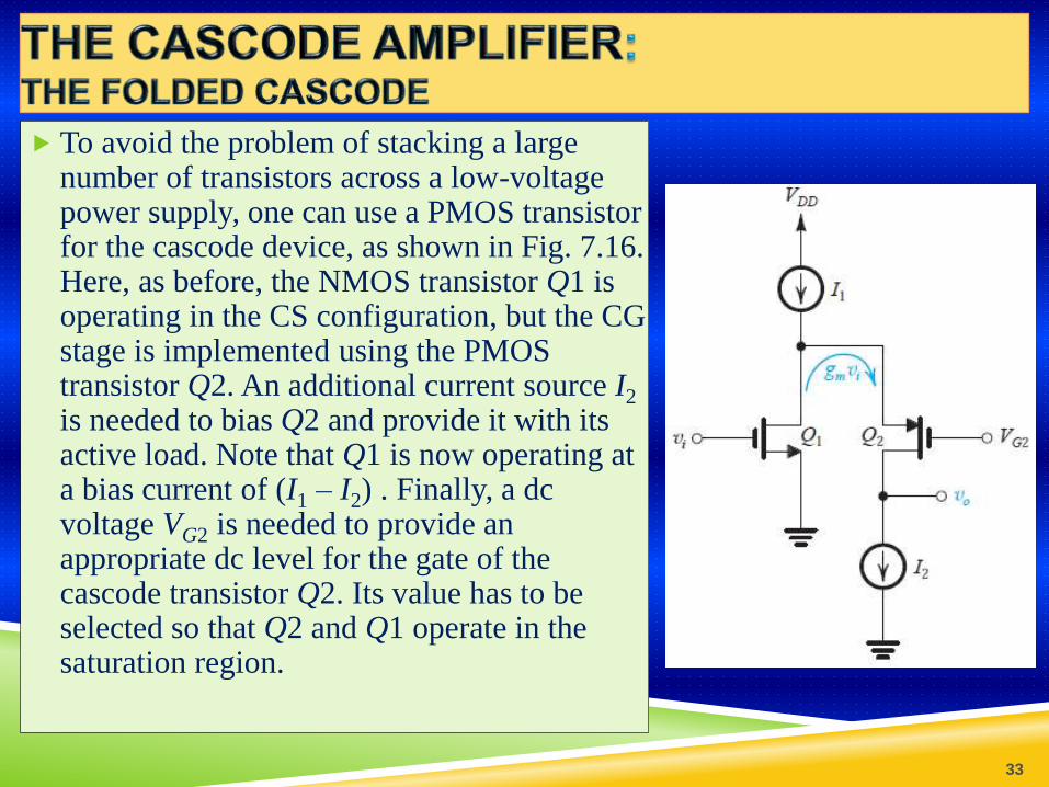
To avoid the problem of stacking a large number of transistors across a low-voltage power supply, one can use a PMOS transistor for the cascode device, as shown in Fig. 7.16. Here, as before, the NMOS transistor Q1 is operating in the CS configuration, but the CG stage is implemented using the PMOS transistor Q2. An additional current source I2
is needed to bias Q2 and provide it with its active load. Note that Q1 is now operating at a bias current of (I1 – I2) . Finally, a dc voltage VG2 is needed to provide an appropriate dc level for the gate of the cascode transistor Q2. Its value has to be selected so that Q2 and Q1 operate in the saturation region.
33
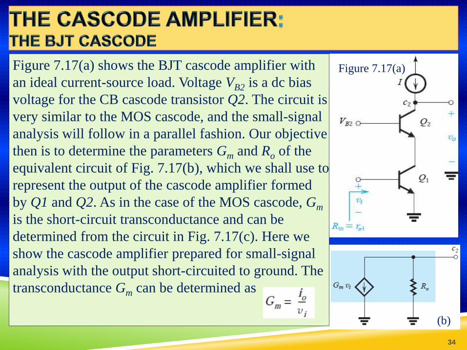
Figure 7.17(a) shows the BJT cascode amplifier with
an ideal current-source load. Voltage VB2 is a dc bias
voltage for the CB cascode transistor Q2. The circuit is
very similar to the MOS cascode, and the small-signal
analysis will follow in a parallel fashion. Our objective
then is to determine the parameters Gm and Ro of the
equivalent circuit of Fig. 7.17(b), which we shall use to
represent the output of the cascode amplifier formed
by Q1 and Q2. As in the case of the MOS cascode, Gm
is the short-circuit transconductance and can be
determined from the circuit in Fig. 7.17(c). Here we
show the cascode amplifier prepared for small-signal
analysis with the output short-circuited to ground. The
transconductance Gm can be determined as
34
Figure 7.17(a)
(b)

Replacing Q1 and Q2 with their hybrid- equivalent-circuit models
gives rise to the circuit in Fig. 7.17(d). Analysis of this circuit is
straightforward and proceeds as follows: The voltage at the node
(c1, e2) is seen to be –vπ .Thus we can write a node equation for
(c1, e2) as
35

Since
we can neglect all the terms beyond the first on the left-hand side to
obtain
Next, we write a node equation at c2
and again neglect the second term on the right-hand side to obtain
Using results in
Thus Gm = gm1 which is the result we have anticipated and is
identical to that for the MOS case.
36
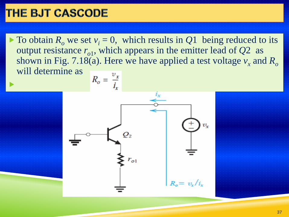
To obtain Ro we set vi = 0, which results in Q1 being reduced to its output resistance ro1, which appears in the emitter lead of Q2 as shown in Fig. 7.18(a). Here we have applied a test voltage vx and Ro
will determine as
37

Replacing Q2 with its hybrid-π model results in the circuit of Fig.
7.18(b). Before embarking on the analysis, it is very useful to
observe first that the current flowing into the emitter node must be
equal to ix. Second, note that ro1 and rπ2 appear in parallel. Thus the
voltage at the emitter node, –vπ2, can be found as
38

39
Since , we can neglect the first term on the
right-hand side of the equation just above.
.
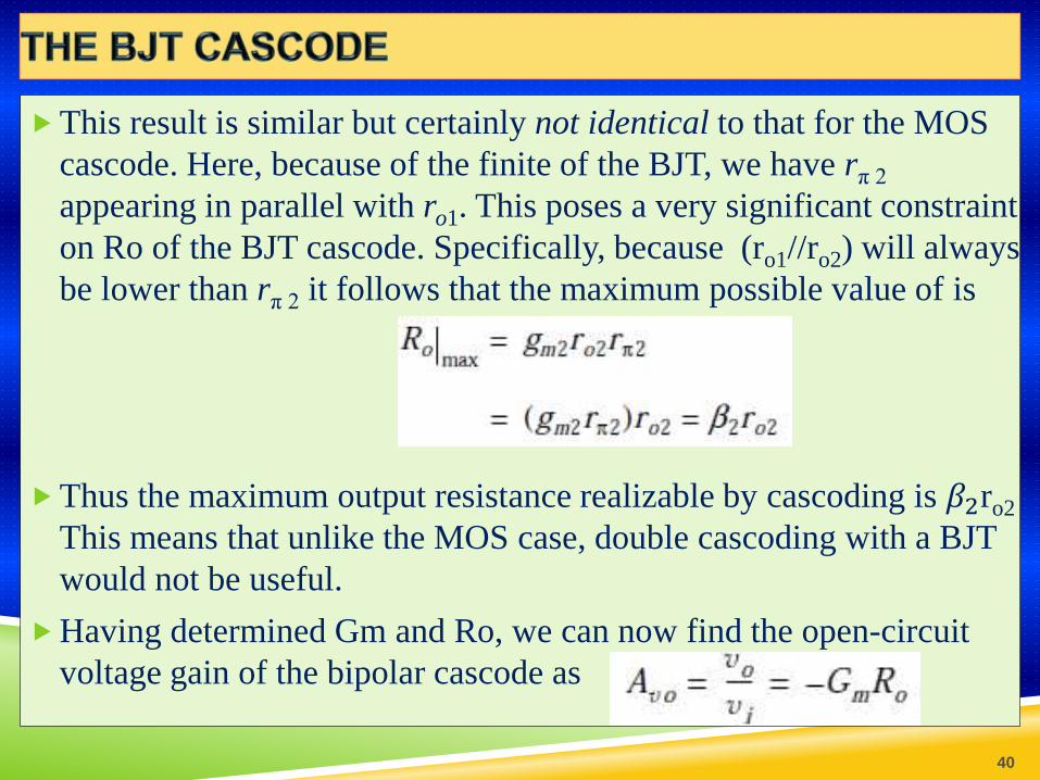
This result is similar but certainly not identical to that for the MOS
cascode. Here, because of the finite of the BJT, we have rπ 2
appearing in parallel with ro1. This poses a very significant constraint
on Ro of the BJT cascode. Specifically, because (ro1//ro2) will always
be lower than rπ 2 it follows that the maximum possible value of is
Thus the maximum output resistance realizable by cascoding is 𝛽2ro2
This means that unlike the MOS case, double cascoding with a BJT
would not be useful.
Having determined Gm and Ro, we can now find the open-circuit
voltage gain of the bipolar cascode as
40
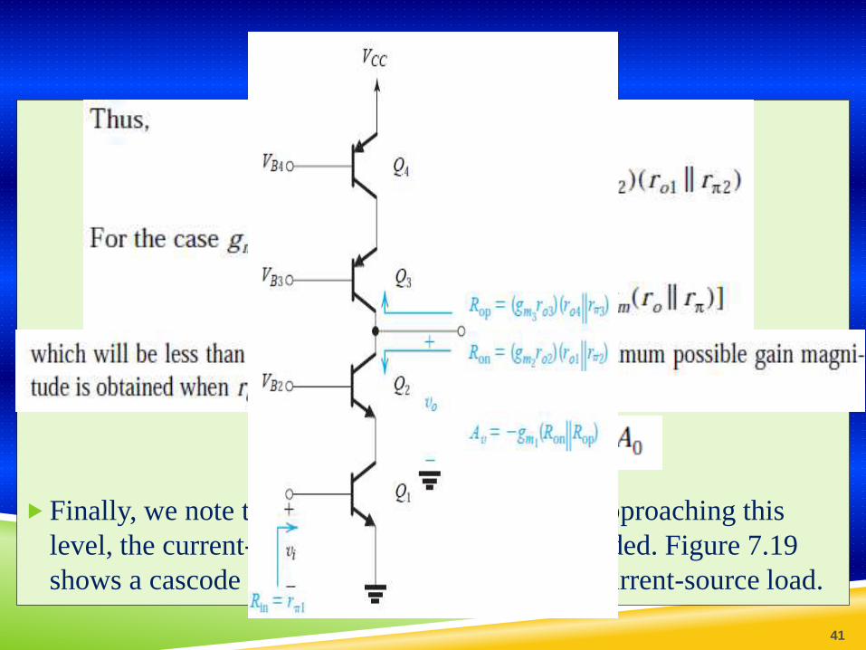
Finally, we note that to be able to realize gains approaching this
level, the current-source load must also be cascoded. Figure 7.19
shows a cascode BJT amplifier with a cascode current-source load.
41
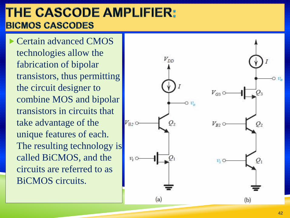
Certain advanced CMOS
technologies allow the
fabrication of bipolar
transistors, thus permitting
the circuit designer to
combine MOS and bipolar
transistors in circuits that
take advantage of the
unique features of each.
The resulting technology is
called BiCMOS, and the
circuits are referred to as
BiCMOS circuits.
42
Figure 7.21 shows two possible BiCMOS cascode amplifiers. The
circuit in Fig. 7.21(a) uses a MOS transistor for the amplifying
device and a BJT for the cascode device. This circuit has the
advantage of an infinite input resistance compared with an input
resistance of rπ obtained in the all-bipolar case. As well, the use of a
bipolar transistor for the cascode stage can result in an increased
output resistance as compared to the all-MOS case [because of the 𝛽bipolar transistor is usually higher than (gmro)of the MOSFET]. The
circuit of Fig. 7.21(b) uses a MOS transistor Q3 to implement double
cascoding. Recall that double cascoding is not possible with BJT
circuits alone.
43
Biasing in integrated-circuit design is based on the use of constant-current sources. On an IC chip with a number of amplifier stages, a constant dc current (called a reference current) is generated at one location and is then replicated at various other locations for biasing the various amplifier stages through a process known as current steering. This approach has the advantage that the effort expended on generating a predictable and stable reference current, usually utilizing a precision resistor external to the chip or a special circuit on the chip, need not be repeated for every amplifier stage. Furthermore, the bias currents of the various stages track each other in case of changes in power-supply voltage or in temperature.
In this section we study circuit building blocks and techniques employed in the bias design of IC amplifiers. These current-source circuits are also utilized as amplifier load elements, as we have seen in
Sections 7.2 and 7.3.
44
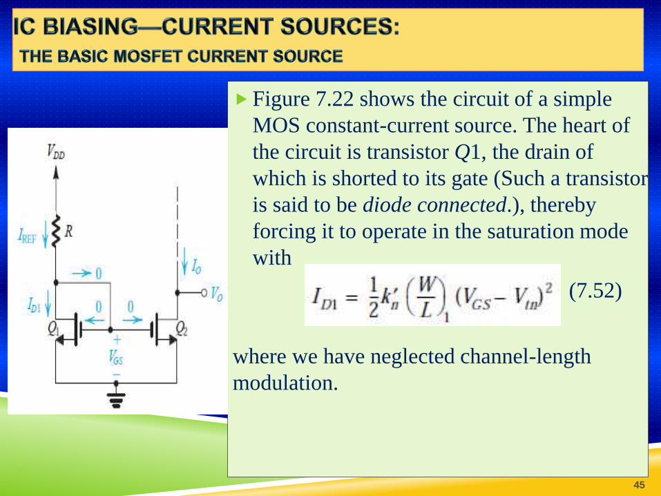
Figure 7.22 shows the circuit of a simple
MOS constant-current source. The heart of
the circuit is transistor Q1, the drain of
which is shorted to its gate (Such a transistor
is said to be diode connected.), thereby
forcing it to operate in the saturation mode
with
(7.52)
where we have neglected channel-length
modulation.
45

THE BASIC MOSFET CURRENT SOURCE
The drain current of Q1 is supplied by VDD
through resistor R, which in most cases
would be outside the IC chip. Since the
gate currents are zero,
(7.53)
where the current through R is considered
to be the reference current of the current
source and is denoted IREF. Equations
(7.52) and (7.53) can be used to determine
the value required for R.
Now consider Q2:
46
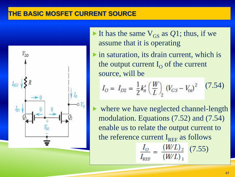
It has the same VGS as Q1; thus, if we
assume that it is operating
in saturation, its drain current, which is
the output current IO of the current
source, will be
(7.54)
where we have neglected channel-length
modulation. Equations (7.52) and (7.54)
enable us to relate the output current to
the reference current IREF as follows
(7.55)
47
THE BASIC MOSFET CURRENT SOURCE

This is a simple and attractive relationship: The special connection
of Q1 and Q2 provides an output current IO that is related to the
reference current IREF by the aspect ratios of the transistors. In other
words, the relationship between IO and IREF is solely determined by
the geometries of the transistors. In the special case of identical
transistors, IO=IREF and the circuit simply replicates or mirrors the
reference current in the output terminal. This has given the circuit
composed Q1 of Q2 and the name current mirror, a name that is
used irrespective of the ratio of device dimensions.
Figure 7.23 depicts the current-mirror circuit with the input reference
current shown as being supplied by a current source for both
simplicity and generality. The current gain or current transfer
ratio of the current mirror is given by Eq. (7.55)
48
THE BASIC MOSFET CURRENT SOURCE
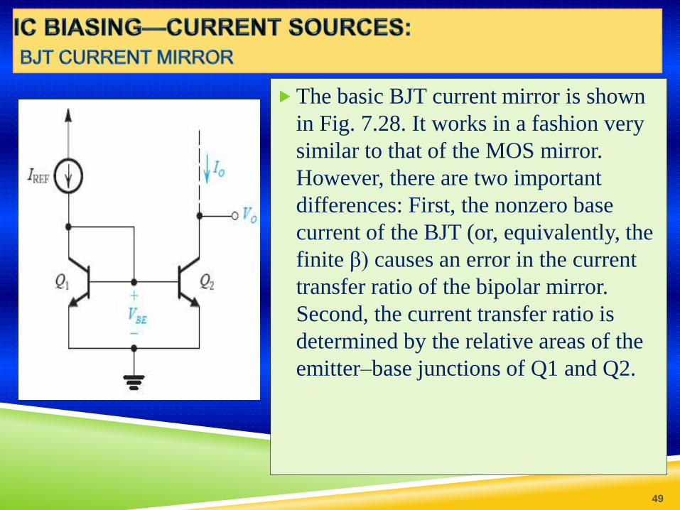
The basic BJT current mirror is shown
in Fig. 7.28. It works in a fashion very
similar to that of the MOS mirror.
However, there are two important
differences: First, the nonzero base
current of the BJT (or, equivalently, the
finite β) causes an error in the current
transfer ratio of the bipolar mirror.
Second, the current transfer ratio is
determined by the relative areas of the
emitter–base junctions of Q1 and Q2.
49

first consider the case:
β sufficiently high
we can neglect the base currents
The reference current IREF is passed through the diode-connected transistor Q1 and thus establishes a corresponding voltage VBE which in turn is applied between base and emitter of Q2. Now, if Q2 is matched to Q1 or, more specifically, if the EBJ area of Q2 is the same as that of Q1, and thus Q2 has the same scale current IS as Q1 then the collector currentof Q2 will be equal to that of Q1; that is,
IO = IREF
50

For this to happen, however, Q2 must be operating in the active
mode, which in turn is achieved as long as the collector voltage VO
is 0.3 V or so higher than that of the emitter. To obtain a current
transfer ratio other than unity, say m, we simply arrange that the area
of the EBJ of Q2 is m times that of Q1.In this case,
IO = m IREF
In general, the current transfer ratio is given by
Alternatively, if the area ratio m is an integer, one can think of as
equivalent to m transistors, each matched to and connected in
parallel.
51

Next we consider the effect of finite
transistor β on the current transfer ratio.
The analysis for the case in which the
current transfer ratio is nominally
unity—that is, for the case in which Q2
is matched to Q1 —is illustrated in Fig.
7.29. The key point here is that since Q1
and Q2 are matched and have the same
VBE their collector currents will be equal.
The rest of the analysis is
straightforward. A node equation at the
collector of Q1 yields
52
Fig. 7.29

Finally, since IO = IC
the current transfer ratio can be found as
Note that as β approaches ∞, IO/IREF
approaches the nominal value of unity.
For typical values of β , however, the
error in the current transfer ratio can be
significant. For instance, results in a 2%
error in the current transfer ratio.
53
Furthermore, the error due to the finite β increases as the nominal
current transfer ratio is increased.
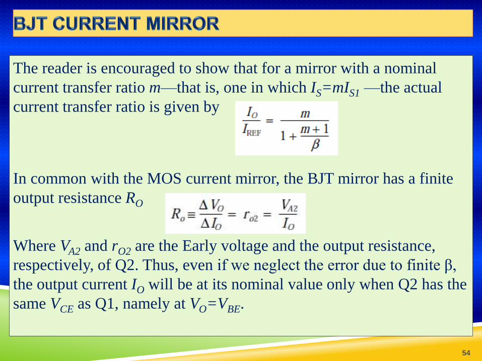
The reader is encouraged to show that for a mirror with a nominal
current transfer ratio m—that is, one in which IS=mIS1 —the actual
current transfer ratio is given by
In common with the MOS current mirror, the BJT mirror has a finite
output resistance RO
Where VA2 and rO2 are the Early voltage and the output resistance,
respectively, of Q2. Thus, even if we neglect the error due to finite β,
the output current IO will be at its nominal value only when Q2 has the
same VCE as Q1, namely at VO=VBE.
54

As VO is increased, IO will correspondingly increase. Taking both the
finite β and the finite RO into account, we can express the output
current of a BJT mirror with a nominal current transfer ratio m as
where we note that the error term due to the Early effect is expressed in
a form that shows that it reduces to zero for VO=VBE
55

56
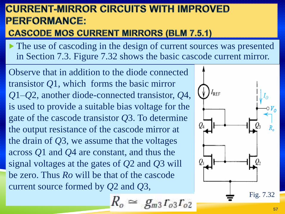
The use of cascoding in the design of current sources was presented in Section 7.3. Figure 7.32 shows the basic cascode current mirror.
57
Observe that in addition to the diode connected
transistor Q1, which forms the basic mirror
Q1–Q2, another diode-connected transistor, Q4,
is used to provide a suitable bias voltage for the
gate of the cascode transistor Q3. To determine
the output resistance of the cascode mirror at
the drain of Q3, we assume that the voltages
across Q1 and Q4 are constant, and thus the
signal voltages at the gates of Q2 and Q3 will
be zero. Thus Ro will be that of the cascode
current source formed by Q2 and Q3,Fig. 7.32
Thus, as expected, cascoding raises the output resistance of the current
source by the factor (gm3ro3), which is the intrinsic gain of the cascode
transistor.
A drawback of the cascode current mirror is that it consumes a
relatively large portion of the steadily shrinking supply voltage VDD.
While the simple MOS mirror operates properly with a voltage as
low as VOV across its output transistor, the cascode circuit of Fig.
7.32 requires a minimum voltage of Vt + 2VOV. This is because the
gate of Q3 is at 2VGS=2Vt+2VOV. Thus the minimum voltage
required across the output of the cascode mirror is 1 V or so. This
obviously limits the signal swing at the output of the mirror (i.e., at
the output of the amplifier that utilizes this current source as a load).
58
The cascode configuration combines CS and CG MOS transistors
(CE and CB bipolar transistors) to great advantage. The key to the
superior performance of the resulting combination is that the
transistor pairing is done in a way that maximizes the advantages
and minimizes the shortcomings of each of the two individual
configurations. In this section we present a number of other such
transistor pairings. In each case the transistor pair can be thought of
as a compound device; thus the resulting amplifier may be
considered as a single stage.
59

Figure 7.38(a) shows an amplifier
formed by cascading a common-collector
(emitter follower) transistor Q1 with a
common-emitter transistor Q2. This
circuit has two main advantages over the
CE amplifier. First, the emitter follower
increases the input resistance by a factor
equal to (β1+1)As a result, the overall
voltage gain is increased, especially if
the resistance of the signal source is
large.
60

The MOS counterpart of the CC–CE amplifier, namely, the CD–CS configuration, is shown in Fig. 7.38(b). Here, since the CS amplifier alone has an infinite input resistance, the sole purpose for adding the source-follower stage is to increase the amplifier bandwidth. Finally, Fig. 7.38(c) shows the BiCMOS version of this circuit type. Compared to the bipolar circuit in Fig. 7.38(a), the BiCMOS circuit has an infinite input resistance. Compared to the MOS circuit in Fig. 7.38(b), the BiCMOScircuit typically has a higher gm2.
61
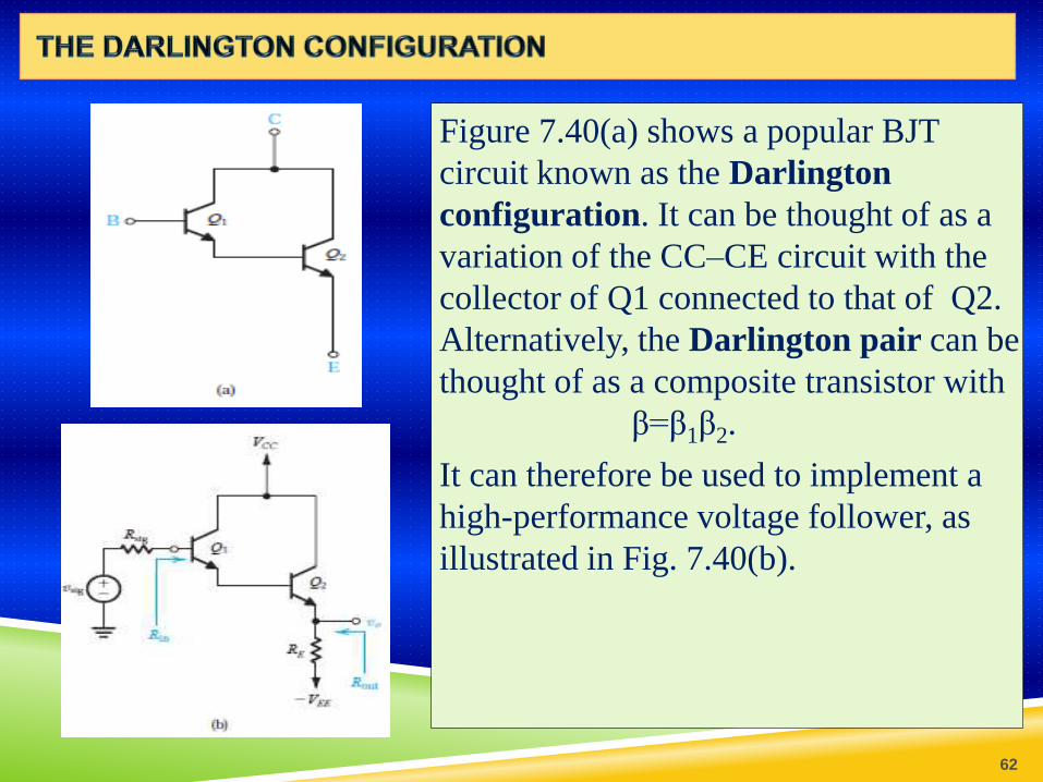
Figure 7.40(a) shows a popular BJT
circuit known as the Darlington
configuration. It can be thought of as a
variation of the CC–CE circuit with the
collector of Q1 connected to that of Q2.
Alternatively, the Darlington pair can be
thought of as a composite transistor with
β=β1β2.
It can therefore be used to implement a
high-performance voltage follower, as
illustrated in Fig. 7.40(b).
62
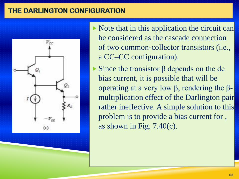
Note that in this application the circuit can
be considered as the cascade connection
of two common-collector transistors (i.e.,
a CC–CC configuration).
Since the transistor β depends on the dc
bias current, it is possible that will be
operating at a very low β, rendering the β-
multiplication effect of the Darlington pair
rather ineffective. A simple solution to this
problem is to provide a bias current for ,
as shown in Fig. 7.40(c).
63
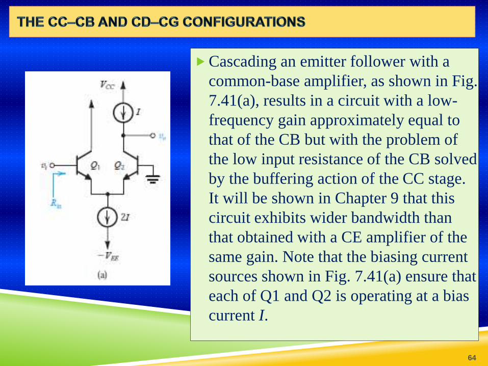
Cascading an emitter follower with a
common-base amplifier, as shown in Fig.
7.41(a), results in a circuit with a low-
frequency gain approximately equal to
that of the CB but with the problem of
the low input resistance of the CB solved
by the buffering action of the CC stage.
It will be shown in Chapter 9 that this
circuit exhibits wider bandwidth than
that obtained with a CE amplifier of the
same gain. Note that the biasing current
sources shown in Fig. 7.41(a) ensure that
each of Q1 and Q2 is operating at a bias
current I.
64
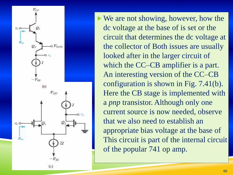
We are not showing, however, how the
dc voltage at the base of is set or the
circuit that determines the dc voltage at
the collector of Both issues are usually
looked after in the larger circuit of
which the CC–CB amplifier is a part.
An interesting version of the CC–CB
configuration is shown in Fig. 7.41(b).
Here the CB stage is implemented with
a pnp transistor. Although only one
current source is now needed, observe
that we also need to establish an
appropriate bias voltage at the base of
This circuit is part of the internal circuit
of the popular 741 op amp.
65

END OF THE CHAPTER
66
Related Documents