Embedded System Lab. II Sound Device Driver in Sound Device Driver in Linux Linux 경희대학교 컴퓨터공학과 조진성 Embedded System Lab. II 2 주요 내용 주요내용 사운드 디바이스 드라이버 제작 디바이스 드라이버를 이용한 응용 프로그램 제작 인터럽트/DMA 등을 활용한 디바이스 드라이버 이해 Embedded System Lab. II 3 디바이스 드라이버 제작 과정 Study Hardware manual 장치 인터페이스 이해 (Registers) 인터럽트 발생의 원인 인지(vector number) 입출력 경로를 알아야 함 Define objective of applications using device Understand interface to related utilities Device setup Device 등록 및 해제 ioctl command Design to adapt to future changes Module Embedded System Lab. II 4 Sound 디바이스 드라이버 Sound 용 Codec chip architecture CS4202 AC’97 Controller Unit Sound Device Driver의 원리 Audio 구동 Mixer madplayer OSS(Open Sound System) Interface를 이용한 Sound Programming

Welcome message from author
This document is posted to help you gain knowledge. Please leave a comment to let me know what you think about it! Share it to your friends and learn new things together.
Transcript

Embedded System Lab. II
Sound Device Driver in Sound Device Driver in LinuxLinux
경희대학교 컴퓨터공학과
조 진 성
Embedded System Lab. II 2
주요내용
주요내용
사운드디바이스드라이버제작
디바이스드라이버를이용한응용프로그램제작
인터럽트/DMA 등을활용한디바이스드라이버이해
Embedded System Lab. II 3
디바이스드라이버제작과정
Study Hardware manual장치인터페이스이해 (Registers)인터럽트발생의원인인지(vector number)입출력경로를알아야함
Define objective of applications using deviceUnderstand interface to related utilities
Device setupDevice 등록및해제ioctl command
Design to adapt to future changesModule
Embedded System Lab. II 4
Sound 디바이스드라이버
Sound 용 Codec chip architectureCS4202AC’97 Controller Unit
Sound Device Driver의원리Audio 구동
Mixermadplayer
OSS(Open Sound System) Interface를이용한 Sound Programming

Embedded System Lab. II 5
CS4202
Embedded System Lab. II 6
AC’97 Controller Unit(ACUNIT)
OverviewAC97 Controller Unit (ACUNIT) of the PXA250 and PXA210 application processors supports the AC97 revision 2.0 features.The ACUNIT also supports audio controller link (AC-link).
AC-link is a serial interface for transferring digital audio, modem, Mic-in, Codec register control, and status information.
The AC97 Codecsends the digitized audio samples that the ACUNIT stores in memory. For playback or synthesized audio production, the processor retrieves stored audio samples and sends them to the Codec through the AC-link. The external digital-to-analog converter (DAC) in the Codec then converts the audio sample to an analog audio waveform.
Embedded System Lab. II 7
AC’97 Controller Unit(ACUNIT)
Supported AC’97 FeaturesIndependent channels for stereo Pulse Code Modulated (PCM) In, Stereo PCM Out, ModemOut, Modem-In and mono Mic-inAll of the above channels support only 16-bit samples in hardware. Samples less than 16 bitsare supported through software.• Multiple sample rate AC97 2.0 Codecs (48 kHz and below). The ACUNIT depends on theCodec to control the varying rate.• Read/write access to AC97 registers• Secondary Codec support• Two Receive FIFOs (32-bit, 16 entries)• Three Transmit FIFOs (32-bit, 16 entries)
Embedded System Lab. II 8
AC’97 Controller Unit(ACUNIT)
Signal DescriptionThe AC97 signals form the AC-link, which is a point-to-point synchronous serial interconnect that supports full-duplex data transfers. All digital audio streams, Modem line Codec streams, and command/status information are communicated over the AC-link.The AC-link uses General Purpose I/Os (GPIOs). Software must reconfigure the GPIOs to use them as the AC-link.

Embedded System Lab. II 9
AC’97 Controller Unit(ACUNIT)
Signal Configuration StepsConfigure SYNC and SDATA_OUT as outputs.Configure BITCLK, SDATA_IN_0, and SDATA_IN_1 as inputs.nACRESET is a dedicated output. It remains asserted on power-up. Complete these steps to deassert nACRESET:
Configure the other AC97 signals as previously described.In the Global Control Register (GCR), Set the GCR[COLD_RST] bit. Refer to
Embedded System Lab. II 10
AC-Link 예
The ACUNIT supports one or two Codecs on the AC-link. SDATA_IN_1 is not needed if only a Primary Codec is connected.
Embedded System Lab. II 11
AC-link Digital Serial Interface Protocol
Each AC97 Codec incorporates a five-pin digital serial interface that links it to the ACUNIT.AC-link is a full-duplex, fixed-clock, PCM digital stream. It employs a time division multiplexed (TDM) scheme to handle control register accesses and multiple input and output audio streams.The AC-link architecture divides each audio frame into 12 outgoing and 12 incoming data streams.Each stream has 20-bit sample resolution and requires a DAC and an analog-to-digital converter(ADC) with a minimum 16-bit resolution.
Embedded System Lab. II 12
Supported Data Stream Formats

Embedded System Lab. II 13
AC-link Digital Serial Interface Protocol
The ACUNIT provides synchronization for all data transaction on the AC-link. A data transaction is made up of 256 bits of information broken up into groups of 13 time slots and is called a frame.Time slot 0 is called the Tag Phase and is 16 bits long.The Tag Phase contains one bit that identifies a valid frame and 12 bits that identify the time slots in the Data Phase that contain valid data.The other 12 time slots are called the Data Phase. Each time slot in the Data Phase is 20 bits long.A frame begins when SYNC goes high. The amount of time that SYNC is high corresponds to the Tag Phase. AC97 frames occur at fixed 48 kHz intervals and are synchronous to the 12.288 MHz bit rate clock, BITCLK.The controller and the Codec use the SYNC and BITCLK to determine when to send transmit data and when to sample receive data. A transmitter transitions the serial data stream on each rising edge of BITCLK and a receiver samples the serial data stream on falling edges of BITCLK.
Embedded System Lab. II 14
AC-link Digital Serial Interface Protocol
The transmitter must tag the valid slots in its serial data stream. The valid slots are tagged in slot 0.Serial data on the AC-link is ordered most significant bit (MSB) to least significant bit (LSB).
The Tag Phase’s first bit is bit 15 and the first bit of each slot in Data Phase is bit 19. The last bit in any slot is bit 0.
Frame = Tag Phase + Data Phase = 13 Slots = 256 bitsTag Phase = Slot 0 = 16 bits, Data Phase = Slot 1 - 12(각20bits)
Embedded System Lab. II 15
AC’97 Controller Unit
AC-link Audio Output Frame(SDATA_OUT)The audio output frame data stream corresponds to the multiplexed bundles that make up the digital output data that targets the AC97 DAC inputs and control registers. Each audio output frame supports up to twelve 20-bit outgoing data time slots.
Embedded System Lab. II 16
AC’97 Controller Unit
Start of Audio Output Frame

Embedded System Lab. II 17
AC’97 Controller Unit
Slot 0: Tag PhaseIn slot 0, the first bit is a global bit (SDATA_OUT slot 0, bit 15) that flags the validity for the entire audio frame.
If the valid frame bit is a 1, the current audio frame contains at least one slot time of valid data.
The next 12 bit positions sampled by AC97 indicate which of the corresponding 12 time slots contain valid data. Bits 0 and 1 of slot 0 are used as Codec ID bits for I/O reads and writes to the Codec registers as described in the next section. Data streams of differing sample rates can be transmitted across AC-link at its fixed 48 kHz audio frame rate. The Codec can control the output sample rate of the controller using the SLOTREQ bits as described later (in the Input frame description).
Embedded System Lab. II 18
AC’97 Controller Unit
Slot 1: Command Address PortThe command port controls features and monitors status for AC97 functions including mixer settings and power management.The control-interface architecture supports up to sixty-four16-bit read/write registers, addressable on even byte boundaries. Audio output frame slot 1 communicates control register address and write/read command information to the ACUNIT.Two Codecs are connected to the single SDATA_OUT. To address the primary and secondary Codecs individually, follow these steps:
To access the primary(secondary) Codec:1. Set the Valid Frame bit (slot 0, bit 15)2. Set the valid bits for slots 1 and 2 (slot 0, bits 14 and 13)3. Write 0b00 to the Codec ID field (slot 0, bits 1 and 0)• secondary 인경우: Write a non-zero value (0b01, 0b10, 0b11) to the Codec ID field
(slot 0, bits 1 and 0)4. Specify the read/write direction of the access (slot 1, bit 19).5. Specify the index to the Codec register (slot 1, bits 18-12)6. If the access is a write, write the data to the command data port (slot 2, bits 19-4)
Embedded System Lab. II 19
AC’97 Controller Unit
Slot 1: Command Address PortFor CODEC reads, the ACUNIT gives the CODEC a maximum of four subsequent frames to respond.if no response is received, the ACUNIT returns a dummy read completion (0xFFFF_FFFF) to the CPU and sets the Read Completion Status (RDCS) bit of the Global Status Register (GSR). The CAIP bit of the CODEC Access Register (CAR) is used to assure that only one I/O cycle occurs across the AC-link at any time. Software must read the CAIP bit before initiating an I/O cycle.If the CAIP bit reads as a one, another driver is performing an I/O cycle.If the CAIP bit reads as a zero, a new I/O cycle can be initiated. The exception to posted accesses is reads to the CODEC GPIO Pin Status register (address 0x54). CODEC GPIO Pin Status read data is sent by the CODEC over the AC-link in the same frame that the read request was sent to the CODEC. The CODEC GPIO Pin Status read data is sent in Slot 12 of the incoming stream. A CODEC with a GPIO Pin Status register must constantly send the status of the register in slot 12.
Embedded System Lab. II 20
AC’97 Controller Unit
Slot 2: Command Data PortSlot 2 (in conjunction with the Command Address Port of Slot 1) delivers 16-bit control register write data in the event that the current command port operation is a write cycle (as indicated by slot 1, bit 19).

Embedded System Lab. II 21
AC’97 Controller Unit
Slot 3: PCM Playback Left Channel Slot 3 contains the composite digital audio left playback stream.
If the playback stream contains an audio sample with a resolution that is less than 20 bits, the ACUNIT fills all trailing non-valid bit positions with zeroes.
Slot 4: PCM Playback Right Channel Slot 4 is the composite digital audio right playback stream.
If the playback stream contains an audio sample with a resolution that is less than 20 bits, the ACUNIT fills all trailing non-valid bit positions with zeroes.
Embedded System Lab. II 22
AC’97 Controller Unit
Slot 5: Modem Line CODECSlot 5 contains the MSB justified modem DAC input data if the modem line CODEC is supported. Slot 6-11: Reserved
Slot 12: I/O ControlSlot 12 contains 16 MSB bits for GPO Status (output).
The following rules govern the use of Slot 12:1. Slot 12 is initially marked invalid by default. 2. A write to address 0x54 in CODEC IO space (using Slot 1 and Slot 2 in the outgoing stream of
the present frame) results in the same write data (sent in Slot 2 of the present outgoing frame) being sent in Slot 12 of the next outgoing frame, where Slot 12 is then marked as valid.
3. After the first write to address 0x54, Slot 12 remains valid for all subsequent frames. The data transmitted on Slot 12 is the data last written to address 0x54. Any subsequent write to the register sends the new data out on the next frame.
4. Following a system reset or AC’97 cold reset, Slot 12 is invalidated. Slot 12 remains invalid until the next write to address 0x54.
Embedded System Lab. II 23
AC’97 Controller Unit
AC-link Audio Input Frame(SDATA_IN)The ACUNIT has two SDATA_IN lines, one primary and one secondary.
Each line can have CODECs attached. The type of CODEC attached determines which slots are valid or invalid. The data slots on the two inputs are completely orthogonal, i.e., no two data slots at the same location will be valid on both lines.
Multiple input data streams are received and multiplexed on slot boundaries as dictated by the slot valid bits in each stream. Each AC-link audio input frame consists of twelve 20-bit time slots.
Slot 0 is reserved and contains 16 bits that are used for AC-link protocol infrastructure.Software must poll the first bit in the audio input frame (SDATA_IN slot 0, bit 15) for an indication that the CODEC is in the CODEC ready state before it places the ACUNIT into data transfer operation. When the “CODEC is ready” state is sampled, the next 12 sampled bits indicate which of the 12 time slots are assigned to input data streams and whether they contain valid data.
Embedded System Lab. II 24
AC’97 Controller Unit
AC’97 Input Frame
Start of an Audio Input Frame

Embedded System Lab. II 25
AC’97 Controller Unit
Slot 0: Tag PhaseIn Slot 0, the first bit is a global bit (SDATA_IN slot 0, bit 15) that indicates whether or not the CODEC is in the CODEC ready state.
If the CODEC Ready bit is a 0, the CODEC is not ready for operation. This condition is normal after power is asserted on reset, i.e., while the CODEC voltage references are settling. When the AC-link CODEC Ready indicator bit is a one, the AC-link and AC’97 control and status registers are fully operational. The ACUNIT must probe the CODEC Powerdown Control/Status register to determine which subsections are ready. The ACUNIT stores CODEC Ready in the PCR bit of the GSR for a primary CODEC and SCR bit of the GSR for a secondary CODEC. Software should monitor PCR or SCR to trigger a DMA or a programmed I/O operation. The ACUNIT only samples CODEC Ready valid once and then ignores it for subsequent frames. CODEC Ready is only resampled after a PR state change.
Embedded System Lab. II 26
AC’97 Controller Unit
Slot 1: Status Address Port/SLOTREQ bits Slot 1 monitors the status of ACUNIT functions including, but not limited to, mixer settings and power management. Slot 1 echoes the control register index for the data to be returned in Slot 2, if the ACUNIT tags Slot 1 and Slot 2 as valid during Slot 0.The ACUNIT only accepts status data (Slot 2 of incoming stream) if the accompanying control register index (Slot 1 of incoming stream) matches the last valid control register index that was sent in Slot 1 of the outgoing stream of the most recent previous frame.
For multiple sample rate output, the CODEC examines its sample-rate control registers, its FIFOs’ states, and the incoming SDATA_OUT tag bits at the beginning of each audio output frame to determine which SLOTREQ bits to set active (low).
Embedded System Lab. II 27
AC’97 Controller Unit
Slot 1: Status Address Port/SLOTREQ bits For multiple sample-rate input, the tag bit for each input slot indicates whether valid data is present.Slot 1 delivers a CODEC control register index and multiple “sample-rate slot request flags” for all output slots. AC’97 defines the ten least significant bits of Slot 1 as CODEC on-demand data request flags for outgoing stream Slots 3-12.
Embedded System Lab. II 28
AC’97 Controller Unit
Slot 2: Status Data PortSlot 2 delivers 16-bit control register read data.

Embedded System Lab. II 29
AC’97 Controller Unit
Slot 3: PCM Record Left Channel Slot 3 contains the CODEC left channel output.
The CODEC transmits its ADC output data (MSB first) and fills any trailing non-valid bit positions with zeroes.
Slot 4: PCM Record Right Channel Slot 4 contains the CODEC right-channel output.
The CODEC transmits its ADC output data (MSB first), and fills any trailing non-valid bit positions with zeroes.
Embedded System Lab. II 30
AC’97 Controller Unit
Slot 5: Optional Modem Line CODECSlot 5 contains MSB justified line modem ADC output data (if the line modem CODEC is supported).
Slot 6: Optional Dedicated Microphone Record DataSlot 6 contains an optional third PCM system-input channel available for dedicated use by a microphone. This input channel supplements a true stereo output to enable a more precise echo-cancellation algorithm for speakerphone applications.
Slot 7-11: ReservedSlot 12: I/O Status
GPIOs which are configured as inputs return their status in Slot 12 of every frame. Only the 16 MSBs are used to return GPIO status.
Bit 0 in the LSBs indicates a GPI Input Interrupt event.The data returned on the latest frame is also accessible to software through the CODEC register at address 0x54 in the modem CODEC I/O space. Data received in Slot 12 is stored internally in the ACUNIT.
Embedded System Lab. II 31
AC’97 Controller Unit
Powering Down the AC-linkThe AC-link signals enter a low power mode after the PR4 bit of the AC’97 CODEC Powerdown Register (0x26) is set to a 1 (by writing 0x1000). Then, the Primary CODEC drives both BITCLK and SDATA_IN to a logic low voltage level.
Embedded System Lab. II 32
AC’97 Controller Unit
Waking up the AC-link

Embedded System Lab. II 33
AC’97 Controller Unit
Waking up the AC-link(Cont’)To wake up the AC-link, a CODEC drives SDATA_IN to a logic high level.
The rising edge triggers the Resume Interrupt if that CODEC’s resume enable bit is set to a one.
The CPU then wakes up the CODEC using the cold or warm reset sequence. The ACUNIT uses a warm reset to wake up the primary CODEC. The CODEC detects a warm reset when SYNC is driven high for a minimum of one microsecond and the BITCLK is absent.
The CODEC must wait until it samples SYNC low before it can start BITCLK. The CODEC that signaled the wake event must keep its SDATA_IN high until it detects that a warm reset has been completed. The CODEC can then transition its SDATA_IN low.
Embedded System Lab. II 34
AC’97 Controller Unit
ACUNIT OperationThe ACUNIT can be accessed through the processor or the DMA controller.
The processor uses programmed I/O instructions to access the ACUNIT, and it can access four register types:
ACUNIT registers: Accessible at 32-bit boundaries.CODEC registers: An audio or modem CODEC can contain up to sixty-four 16-bit registers. A CODEC uses a 16-bit address boundary for registers. The ACUNIT supplies access to the CODEC registers by mapping them to its 32-bit address domain boundary.Modem CODEC GPIO register: If the ACUNIT is connected to a modemCODEC, the CODEC GPIO register can also be accessed. The CODEC GPIO register uses access address 0x0054 in the CODEC domain. ACUNIT FIFO data: The ACUNIT has two Transmit FIFOs for audio-out and modem-out and three receive FIFOs for audio-in, modem-in, and mic-in. Data enters the transmit FIFOs by writing to either the PCM Data Register (PCDR) or the Modem Data Register (MODR).
Embedded System Lab. II 35
AC’97 Controller Unit
ACUNIT OperationOnly the DMA can access the FIFOs.
The DMA controller accesses FIFO data in 8-, 16-, or 32- byte blocks. The ACUNIT makes a transmit DMA request when the transmit FIFO has less than 32 bytes. The ACUNIT makes a receive DMA request when the receive FIFO has 32 bytes or more. Regardless of burst size, the DMA descriptor length must be a multiple of 32 bytes to prevent audio artifacts from being introduced onto the AC-link. The DMA controller responds to the following ACUNIT DMA requests:
PCM FIFO transmit and receive DMA requests made when the PCM transmit and receive FIFOs are half full. Modem FIFO transmit and receive DMA requests made when the modemtransmit and receive FIFOs are half full. Mic-in receive DMA requests made when the Mic-in receive FIFO is half full.
Embedded System Lab. II 36
AC’97 Controller Unit
InitializationAfter power up, the nACRESET signal remains asserted until the audio or modem driver sets the COLD_RST bit of the GCR to one.To initialize the ACUNIT follow theses steps: 1. Program the GPIO Direction register and GPIO Alternate Function Select register to assign
proper pin directions for the ACUNIT ports. 2. Set the COLD_RST bit of the GCR to one to deassert nACRESET. Deasserting nACRESET has
the following effects: a. Frames filled with zeroes are transmitted because the transmit FIFO is still empty. This situation
does not cause an error condition. b. The ACUNIT records zeroes until the CODEC sends valid data. c. DMA requests are enabled. 3. Enable the Primary Ready Interrupt Enable and/or the Secondary Ready Interrupt Enable by
setting the PRIRDY_IEN bit and/or the SECRDY_IEN bit of the GCR to one. 4. Software enables DMA operation in response to primary and secondary ready interrupts. 5. The ACUNIT triggers transmit DMA requests. The DMA fills the transmit FIFO in response. 6. The ACUNIT continues to transmit zeroes until the transmit FIFO is half full. When it is half full,
valid transmit FIFO data is sent across the AC-link.

Embedded System Lab. II 37
AC’97 Controller Unit
Operational Flow for Accessing CODEC Registers Software accesses the CODEC registers by translating a 32-bit processor physical address to a 7-bit CODEC address.Software must read the CODEC Access Register (CAR) to lock the AC-link. The AC-link is free if the CAIP bit of the CAR is zero.
A read access to the CAR sets the CAIP bit. The ACUNIT clears the CAIP bit when the CODEC-write or CODEC-read operation completes. Software can also clear the CAIP bit by writing a zero to it. After it locks the AC-link, software can write or read a CODEC register using the appropriate processor physical address. The ACUNIT sets the CDONE bit of the GSR to one after the completion of a CODEC write operation. Software clears this bit by writing a 1 to it.
Embedded System Lab. II 38
AC’97 Controller Unit
Operational Flow for Accessing CODEC Registers To read a CODEC, the software must complete the following steps:1. Software issues a dummy read to the CODEC register.
The ACUNIT responds to this read operation with invalid data. The ACUNIT then initiates the read access across the AC-link.
2. When the CODEC read operation completes, the ACUNIT sets the SDONE bit of the GSR to one. Software clears this bit by writing a 1 it.
3. Software repeats the read operation as detailed in Step 1. The ACUNIT now returns the data sent by the CODEC. The second read operation also initiates a read access across the AC-link.
4. The ACUNIT times-out the read operation if the CODEC fails to respond in four SYNC frames. In this case, the second read operation returns a timed-out data value of 0x0000_FFFF.
Embedded System Lab. II 39
ACUNIT: Functional Description
FIFOsThe ACUNIT has five FIFOs:
PCM Transmit FIFO, with sixteen 32-bit entries.PCM Receive FIFO, with sixteen 32-bit entries.Modem Transmit FIFO, with sixteen 32-bit entries (upper 16 bits must always be zero).Modem Receive FIFO, with sixteen 32-bit entries (upper 16 bits are always zero).Mic-in Receive FIFO, with sixteen 32-bit entries (upper 16 bits are always zero).
A receive FIFO triggers a DMA request when the FIFO has eight or more entries. A transmit FIFO triggers a DMA request when it holds less than eight entries. A transmit FIFO must be half full (filled with eight entries) before any data is transmitted across the AC-link.
Embedded System Lab. II 40
ACUNIT: Functional Description
InterruptsThe following status bits interrupt the processor when the interrupts are enabled:
Mic-in FIFO error: Mic-in Receive FIFO’s over-run or under-run error.Modem-in FIFO error: Modem Receive FIFO’s over-run or under-run error.PCM-in FIFO error: Audio Receive FIFO’s over-run or under-run error.Modem-out FIFO error: Modem Transmit FIFO’s over-run or under-run error.PCM-out FIFO error: Audio Transmit FIFO’s over-run or under-run error.Modem CODEC GPI status change interrupt: Interrupts the CPU if bit 0 of Slot 12 is set. This indicates a change in one of the bits in the modem CODEC’s GPIO register.Primary CODEC resume interrupt: Sets a status register bit when the Primary CODEC resumes from a lower power mode. Software writes a one to this bit to clear it.

Embedded System Lab. II 41
ACUNIT: Functional Description
Interrupts(2)Secondary CODEC resume interrupt: Sets a status register bit when the Secondary CODEC resumes from a lower power mode. Software writes a one to this bit to clear it.CODEC command done interrupt: Interrupts the CPU when a CODEC register’s command is completed. Software writes a one to this bit to clear it.CODEC status done interrupt: Interrupts the CPU when a CODEC register’s status address and data reception are completed. Software writes a one to this bit to clear it.Primary CODEC ready interrupt: Sets a status register bit when the Primary CODEC is ready. The CODEC sets bit 0 of Slot 0 on the input frame to signal that it is ready. Software clears the PRIRDY_IEN bit of the GCR to clear this interrupt.Secondary CODEC ready interrupt: Sets a status register bit when the Secondary CODEC is ready. The CODEC sets bit 0 of Slot 0 on the input frame to signal that it is ready. Software clears the SECRDY_IEN bit of the GCR to clear this interrupt.
Embedded System Lab. II 42
ACUNIT: Functional Description
RegistersThe ACUNIT and CODEC registers are mapped in addresses ranging from 0x4050_0000 through 0x405F_FFFF. They are accessed via a 32-bit address map and translated to 16-bits for the CODEC.Programmed I/O and DMA bursts can access the following registers:
Global registers: The ACUNIT has three global registers:Status, Control, and CODEC access registers that are common to the audio and modem domains.
Channel-specific audio ACUNIT registers refer to PCM-out, PCM-in, and mic-in channels.Channel-specific Modem ACUNIT registers refer to modem-out and modem-in channels.Audio CODEC registersModem CODEC registers
Embedded System Lab. II 43
AC’97 Controller Unit
Codec Access Register
Embedded System Lab. II 44
Sound Device Driver 함수개요
mixer_fops mixer_ioctl
ac97_audio_state.dev_dsp = register_sound_dsp(&ac97_audio_fops)
ac97_audio_fops
pxa_audio_attach
pxa_ac97_init pxa_ac97_get pxa_ac97_irq(IRQ_AC97, pxa_ac97_irq,…)
pxa_ac97_codec.dev_mixer = register_sound_mixer(&mixer_fops)
pxa_request_dma(.. audio_dma_irq...)
filep->f_op->release,write,read,mmap,poll,ioctl,llseek= audio_release, audio_write, audio_read,
audio_mmap, audio_ioctl,..
ac97_audio_open ac97_audio_attach

Embedded System Lab. II 45
Sound Device Driver의원리
pxa-ac97.c source 분석static u16 pxa_ac97_read(struct ac97_codec *codec, u8 reg){
u16 val = -1;
down(&CAR_mutex);if (!(CAR & CAR_CAIP)) {
volatile u32 *reg_addr = (u32 *)&PAC_REG_BASE + (reg >> 1);
waitingForMask=GSR_SDONE;
init_completion(&CAR_completion);//start read access across the ac97 link(void)*reg_addr;
wait_for_completion(&CAR_completion);
0x40500200 : primary audio codec
Embedded System Lab. II 46
Sound Device Driver의원리
pxa-ac97.c source 분석 (Cont’)
Each CODEC has up to sixty-four 16-bit registers that are addressable internal to the CODEC at half-word boundaries(16-bit boundaries). Because the processor only supports internal register accesses at word boundaries (32-bit boundaries), software must select the one of the following formulas to translate a 7-bit CODEC address into a 32-bit processor address:
Processor physical address for a Primary Audio CODEC = 0x4050-0200 + Shift_Left_Once(Internal 7-bit CODEC Register Address)Processor physical address for a Secondary Audio CODEC = 0x4050-0300 + Shift_Left_Once(Internal 7-bit CODEC Register Address)Processor physical address for a Primary Modem CODEC = 0x4050-0400 + Shift_Left_Once(Internal 7-bit CODEC Register Address)Processor physical address for a Secondary Modem CODEC = 0x4050-0500 + Shift_Left_Once(Internal 7-bit CODEC Register Address)
Embedded System Lab. II 47
Sound Device Driver의원리
pxa-ac97.c source 분석 (Cont’)
if (GSR & GSR_RDCS) {GSR |= GSR_RDCS;
printk(KERN_CRIT __FUNCTION__": read codec register timeout.\n");
}
init_completion(&CAR_completion);val = *reg_addr;
wait_for_completion(&CAR_completion);
} else {printk(KERN_CRIT __FUNCTION__": CAR_CAIP already set\n");
}up(&CAR_mutex);return val;
}
cleared by software writing a ‘1’ to this location
Embedded System Lab. II 48
Sound Device Driver의원리
pxa-ac97.c source 분석 (Cont’)static void pxa_ac97_write(struct ac97_codec *codec, u8 reg, u16 val){
down(&CAR_mutex);if (!(CAR & CAR_CAIP)) {
volatile u32 *reg_addr= (u32 *)&PAC_REG_BASE + reg >>1);waitingForMask=GSR_CDONE;init_completion(&CAR_completion);*reg_addr = val;wait_for_completion(&CAR_completion);
} else {printk(KERN_CRIT __FUNCTION__": CAR_CAIP already set\n");
}up(&CAR_mutex);
}
0x40500200 : primary audio codec

Embedded System Lab. II 49
Sound Device Driver의원리
pxa-ac97.c source 분석 (Cont’)
static void pxa_ac97_irq(int irq, void *dev_id, struct pt_regs *regs){
int gsr = GSR;GSR = gsr & (GSR_SDONE|GSR_CDONE);if (gsr & waitingForMask){
complete(&CAR_completion);}
}
Embedded System Lab. II 50
Sound Device Driver의원리
pxa-ac97.c source 분석 (Cont’)
static struct ac97_codec pxa_ac97_codec = {codec_read: pxa_ac97_read,codec_write: pxa_ac97_write,
};
static DECLARE_MUTEX(pxa_ac97_mutex);static int pxa_ac97_refcount;
Embedded System Lab. II 51
Sound Device Driver의원리
pxa-ac97.c source 분석 (Cont’)int pxa_ac97_get(struct ac97_codec **codec){
int ret;
*codec = NULL;down(&pxa_ac97_mutex);
if (!pxa_ac97_refcount) {ret = request_irq(IRQ_AC97, pxa_ac97_irq, 0, "AC97", NULL);if (ret)
return ret;
Embedded System Lab. II 52
Sound Device Driver의원리
pxa-ac97.c source 분석 (Cont’)CKEN |= CKEN2_AC97; set_GPIO_mode(GPIO31_SYNC_AC97_MD);set_GPIO_mode(GPIO30_SDATA_OUT_AC97_MD);set_GPIO_mode(GPIO28_BITCLK_AC97_MD);set_GPIO_mode(GPIO29_SDATA_IN_AC97_MD);
GCR = 0;udelay(10);GCR = GCR_COLD_RST|GCR_CDONE_IE|GCR_SDONE_IE;while (!(GSR & GSR_PCR)) {
schedule();}

Embedded System Lab. II 53
Sound Device Driver의원리
pxa-ac97.c source 분석 (Cont’)ret = ac97_probe_codec(&pxa_ac97_codec);if (ret != 1) {
free_irq(IRQ_AC97, NULL);GCR = GCR_ACLINK_OFF;CKEN &= ~CKEN2_AC97; return ret;
}pxa_ac97_write(&pxa_ac97_codec,AC97_EXTENDED_STATUS,1);
pxa_ac97_write(&pxa_ac97_codec, 0x6a, 0x0050);pxa_ac97_write(&pxa_ac97_codec, 0x6c, 0x0030);
}pxa_ac97_refcount++;up(&pxa_ac97_mutex);*codec = &pxa_ac97_codec;return 0;
Embedded System Lab. II 54
Sound Device Driver의원리
pxa-ac97.c source 분석 (Cont’)void pxa_ac97_put(void){
down(&pxa_ac97_mutex);pxa_ac97_refcount--;if (!pxa_ac97_refcount) {
GCR = GCR_ACLINK_OFF;CKEN &= ~CKEN2_AC97; free_irq(IRQ_AC97, NULL);
}up(&pxa_ac97_mutex);
}
EXPORT_SYMBOL(pxa_ac97_get);EXPORT_SYMBOL(pxa_ac97_put);
Embedded System Lab. II 55
Sound Device Driver의원리
pxa-ac97.c source 분석 (Cont’)
static int ac97_audio_open(struct inode *inode, struct file *file){
return pxa_audio_attach(inode, file, ac97_audio_state);}
static struct file_operations ac97_audio_fops = {open: ac97_audio_open,owner: THIS_MODULE
};
Embedded System Lab. II 56
Sound Device Driver의원리
pxa-ac97.c source 분석 (Cont’)static int __init pxa_ac97_init(void){
int ret;struct ac97_codec *dummy;
ret = pxa_ac97_get(&dummy);if (ret)
return ret;
ac97_audio_state.dev_dsp = register_sound_dsp(&ac97_audio_fops, -1);pxa_ac97_codec.dev_mixer = register_sound_mixer(&mixer_fops, -1);
return 0;}
Minor number를자동으로잡아준
다.

Embedded System Lab. II 57
Sound Device Driver의원리
pxa-ac97.c source 분석 (Cont’)
static void __exit pxa_ac97_exit(void){
unregister_sound_dsp(ac97_audio_state.dev_dsp);unregister_sound_mixer(pxa_ac97_codec.dev_mixer);pxa_ac97_put();
}module_init(pxa_ac97_init);module_exit(pxa_ac97_exit);
Insmod실행시호출 :모듈을커널에등록
rmmod시호출
Embedded System Lab. II 58
Sound Device Driver의원리
pxa-audio.c source 분석
void pxa_audio_clear_buf(audio_stream_t * s){
DECLARE_WAITQUEUE(wait, current);int frag;
if (!s->buffers)return;
/* Ensure DMA isn't running */set_current_state(TASK_UNINTERRUPTIBLE);add_wait_queue(&s->stop_wq, &wait);DCSR(s->dma_ch) = DCSR_STOPIRQEN;schedule();remove_wait_queue(&s->stop_wq, &wait);
Embedded System Lab. II 59
Sound Device Driver의원리
pxa-audio.c source 분석(cont’d)
/* free DMA buffers */for (frag = 0; frag < s->nbfrags; frag++) {
audio_buf_t *b = &s->buffers[frag];if (!b->master)
continue;consistent_free(b->data, b->master, b->dma_desc->dsadr);
}
/* free descriptor ring */if (s->buffers->dma_desc)
consistent_free(s->buffers->dma_desc, s->nbfrags * s->descs_per_frag * DMA_DESC_SIZE,s->dma_desc_phys);
/* free buffer structure array */kfree(s->buffers);s->buffers = NULL;
}
Embedded System Lab. II 60
Sound Device Driver의원리
pxa-audio.c source 분석(cont’d)
static int audio_set_fragments(audio_stream_t *s, int val){
if (s->mapped || DCSR(s->dma_ch) & DCSR_RUN)return -EBUSY;
if (s->buffers)audio_clear_buf(s);
s->nbfrags = (val >> 16) & 0x7FFF;val &= 0xffff;if (val < 5)
val = 5;if (val > 15)
val = 15;
Device or resource is busy

Embedded System Lab. II 61
Sound Device Driver의원리
pxa-audio.c source 분석(cont’d)
s->fragsize = 1 << val;if (s->nbfrags < 2)
s->nbfrags = 2;if (s->nbfrags * s->fragsize > 256 * 1024)
s->nbfrags = 256 * 1024 / s->fragsize;if (audio_setup_buf(s))
return -ENOMEM;return val|(s->nbfrags << 16);
}
Embedded System Lab. II 62
Sound Device Driver의원리
pxa-audio.c source 분석(cont’d)
static int audio_write(struct file *file, const char *buffer,size_t count, loff_t * ppos)
{const char *buffer0 = buffer;audio_state_t *state = (audio_state_t *)file->private_data;audio_stream_t *s = state->output_stream;int chunksize, ret = 0;
if (ppos != &file->f_pos)return -ESPIPE;
if (s->mapped)return -ENXIO;
if (!s->buffers && audio_setup_buf(s))return -ENOMEM;
Embedded System Lab. II 63
Sound Device Driver의원리
pxa-audio.c source 분석(cont’d)while (count > 0) {
audio_buf_t *b = &s->buffers[s->usr_frag];
/* Grab a fragment */if (file->f_flags & O_NONBLOCK) {
ret = -EAGAIN;if (down_trylock(&s->sem))
break;} else {
ret = -ERESTARTSYS;if (down_interruptible(&s->sem))
break;}/* Feed the current buffer */chunksize = s->fragsize - b->offset;if (chunksize > count)
chunksize = count;
Embedded System Lab. II 64
Sound Device Driver의원리
pxa-audio.c source 분석(cont’d)if (copy_from_user(b->data + b->offset, buffer, chunksize)) {
up(&s->sem);return -EFAULT;
}b->offset += chunksize;buffer += chunksize;count -= chunksize;if (b->offset < s->fragsize) {
up(&s->sem);break;
}/*activate DMA on current buffer*/b->offset = 0;b->dma_desc->ddadr &= ~DDADR_STOP;if (DCSR(s->dma_ch) & DCSR_STOPSTATE) {
DDADR(s->dma_ch) = b->dma_desc->ddadr;DCSR(s->dma_ch) = DCSR_RUN;
}

Embedded System Lab. II 65
Sound Device Driver의원리
pxa-audio.c source 분석(cont’d)/* move the index to the next fragment */
if (++s->usr_frag >= s->nbfrags)s->usr_frag = 0;
}
if ((buffer - buffer0))ret = buffer - buffer0;
return ret;}
Embedded System Lab. II 66
Sound Device Driver의원리
pxa-audio.c source 분석(cont’d)
static int audio_read(struct file *file, char *buffer, size_t count, loff_t * ppos)
{char *buffer0 = buffer;audio_state_t *state = file->private_data;audio_stream_t *s = state->input_stream;int chunksize, ret = 0;
if (ppos != &file->f_pos)return -ESPIPE;
if (s->mapped)return -ENXIO;
if (!s->buffers && audio_setup_buf(s))return -ENOMEM;
Embedded System Lab. II 67
Sound Device Driver의원리
pxa-audio.c source 분석(cont’d)while (count > 0) {
audio_buf_t *b = &s->buffers[s->usr_frag];/* prime DMA */
if (DCSR(s->dma_ch) & DCSR_STOPSTATE) {DDADR(s->dma_ch) =
s->buffers[s->dma_frag].dma_desc->ddadr;DCSR(s->dma_ch) = DCSR_RUN;
}/* Wait for a buffer to become full */
if (file->f_flags & O_NONBLOCK) {ret = -EAGAIN;if (down_trylock(&s->sem)) break;
} else {ret = -ERESTARTSYS;if (down_interruptible(&s->sem))
break;}
Embedded System Lab. II 68
Sound Device Driver의원리
pxa-audio.c source 분석(cont’d)
/* Grab data from current buffer */chunksize = s->fragsize - b->offset;if (chunksize > count)
chunksize = count;if (copy_to_user(buffer, b->data + b->offset, chunksize)) {
up(&s->sem);return -EFAULT;
}b->offset += chunksize;buffer += chunksize;count -= chunksize;if (b->offset < s->fragsize) {
up(&s->sem);break;
}

Embedded System Lab. II 69
Sound Device Driver의원리
pxa-audio.c source 분석(cont’d)
b->offset = 0;b->dma_desc->ddadr &= ~DDADR_STOP;
/* move the index to the next fragment */if (++s->usr_frag >= s->nbfrags)
s->usr_frag = 0;}if ((buffer - buffer0))
ret = buffer - buffer0;return ret;
}
Embedded System Lab. II 70
Sound Device Driver의원리
pxa-audio.c source 분석(cont’d)
static int audio_release(struct inode *inode, struct file *file){
audio_state_t *state = file->private_data;
down(&state->sem);
if (file->f_mode & FMODE_READ) {audio_clear_buf(state->input_stream);*state->input_stream->drcmr = 0;pxa_free_dma(state->input_stream->dma_ch);state->rd_ref = 0;
}
Embedded System Lab. II 71
Sound Device Driver의원리
pxa-audio.c source 분석(cont’d)
if (file->f_mode & FMODE_WRITE) {audio_sync(file);audio_clear_buf(state->output_stream);*state->output_stream->drcmr = 0;pxa_free_dma(state->output_stream->dma_ch);state->wr_ref = 0;
}
up(&state->sem);return 0;
}
Embedded System Lab. II 72
Sound Device Driver의원리
pxa-audio.c source 분석(cont’d)
int pxa_audio_attach(struct inode *inode, struct file *file, audio_state_t *state)
{audio_stream_t *is = state->input_stream;audio_stream_t *os = state->output_stream;int err;
down(&state->sem);
/* access control */err = -ENODEV;if ((file->f_mode & FMODE_WRITE) && !os)
goto out;if ((file->f_mode & FMODE_READ) && !is)
goto out;

Embedded System Lab. II 73
Sound Device Driver의원리
pxa-audio.c source 분석(cont’d)
err = -EBUSY;if ((file->f_mode & FMODE_WRITE) && state->wr_ref)
goto out;if ((file->f_mode & FMODE_READ) && state->rd_ref)
goto out;
/* request DMA channels */if (file->f_mode & FMODE_WRITE) {
err = pxa_request_dma(os->name, DMA_PRIO_LOW, audio_dma_irq, os);
if (err < 0)goto out;
os->dma_ch = err;}
Embedded System Lab. II 74
Sound Device Driver의원리
pxa-audio.c source 분석(cont’d)
if (file->f_mode & FMODE_READ) {err = pxa_request_dma(is->name, DMA_PRIO_LOW,
audio_dma_irq, is);if (err < 0) {
if (file->f_mode & FMODE_WRITE) {*os->drcmr = 0;pxa_free_dma(os->dma_ch);
}goto out;
}is->dma_ch = err;
}file->private_data = state;file->f_op->release = audio_release;file->f_op->write = audio_write;file->f_op->read = audio_read;file->f_op->mmap = audio_mmap;file->f_op->poll = audio_poll;file->f_op->ioctl = audio_ioctl;file->f_op->llseek = no_llseek;
Embedded System Lab. II 75
Sound Device Driver의원리
pxa-audio.c source 분석(cont’d)if ((file->f_mode & FMODE_WRITE)) {
state->wr_ref = 1;os->fragsize = AUDIO_FRAGSIZE_DEFAULT;os->nbfrags = AUDIO_NBFRAGS_DEFAULT;os->output = 1;os->mapped = 0;init_waitqueue_head(&os->frag_wq);init_waitqueue_head(&os->stop_wq);*os->drcmr = os->dma_ch | DRCMR_MAPVLD;
}if (file->f_mode & FMODE_READ) {
state->rd_ref = 1;is->fragsize = AUDIO_FRAGSIZE_DEFAULT;is->nbfrags = AUDIO_NBFRAGS_DEFAULT;is->output = 0;is->mapped = 0;init_waitqueue_head(&is->frag_wq);init_waitqueue_head(&is->stop_wq);*is->drcmr = is->dma_ch | DRCMR_MAPVLD;
}
8192
8
Embedded System Lab. II 76
Sound Device Driver의원리
pxa-audio.c source 분석(cont’d)
err = 0;
out:up(&state->sem);return err;
}
EXPORT_SYMBOL(pxa_audio_attach);EXPORT_SYMBOL(pxa_audio_clear_buf);

Embedded System Lab. II 77
Audio 구동
mixer
/dev 디렉토리에가면 mixer가있음을확인할수있다.
Embedded System Lab. II 78
Audio 구동
mixer
$mixer vol 30 이라고입력하면 volume을설정할수있음
Embedded System Lab. II 79
Audio 구동
mixer
pcm볼륨를설정할수있음
Embedded System Lab. II 80
Sound 관련응용프로그램
Sound driver를이용한응용프로그램madplay를이용한실제적용
madplay파일다운로드출처http://sourceforge.net/project/showfiles.php?group_id=12349
madplay를설치하기위해서는다음의 4가지파일필요

Embedded System Lab. II 81
madplay설치(1)
zlib-1.1.4.tar.gz 압축해제
Embedded System Lab. II 82
madplay설치(2)
madplay-0.15.2b.tar.gz 압축해제
Embedded System Lab. II 83
madplay설치(3)
libmad-0.15.1b.tar.gz 압축해제
Embedded System Lab. II 84
madplay설치(4)
libid3tag-0.15.1b.tar.gz 압축해제

Embedded System Lab. II 85
madplay설치(5)
크로스컴파일을위해 shell 설정파일수정(.bashrc)configure 작업시환경변수를참조하여크로스컴파일이가능하게하기위해설정
CPPFLAGS=‘–I../libid3tag-0.15.1b –I../libmad-0.15.1b –I../zlib-1.1.4 –I/usr/local/hybus-arm-linux-R1.1/arm-linux/include –I/usr/include’
LDFLAGS=‘–I../libid3tag-0.15.1b –I../libmad-0.15.1b –I../zlib-1.1.4’
Embedded System Lab. II 86
madplay설치(6)
zlib-1.1.4 디렉토리로들어가서 configure 및 make실행
# make installmake 이후 make install을해준다.
Embedded System Lab. II 87
madplay설치(7)
libid3tag-0.15.1b 디렉토리로들어가서 configure 실행
./configure시 –host=arm=arm-linux옵션을준다.
Embedded System Lab. II 88
madplay설치(8)
libid3tag-0.15.1b 디렉토리로들어가서 make 실행
# make
컴파일된라이브러리를현재make한디렉토리로이동시킨다.

Embedded System Lab. II 89
madplay설치(9)
libmad-0.15.1b 디렉토리로들어가서 configure 실행
./configure시 –host=arm=arm-linux옵션을준다.
Embedded System Lab. II 90
madplay설치(10)
libmad-0.15.1b 디렉토리로들어가서 make 실행
# make
컴파일된라이브러리를현재make한디렉토리로이동시킨다.
Embedded System Lab. II 91
madplay설치(11)
madplay-0.15.2b 디렉토리로들어가서 configure 실행
./configure시 –host=arm=arm-linux옵션을준다.
Embedded System Lab. II 92
madplay설치(12)
madplay-0.15.2b 디렉토리로들어가서 make 실행
생성된실행파일을확인한다.

Embedded System Lab. II 93
madplay설치(13)
arm 보드에서실행보드에달린사운드포트에서음악이출력되면성공
./mplay sample.mp3
실행시 libmad.a, libid3tag.a 라이브러리가필요하므로라이브러리경로를잡아주거나타겟의디폴트라이브러리위치로복사한다.
타겟보드로복사했을때는libmad.a는 libmad.so.0로,libid3tag.a는 libid3tag.so.0로심볼링크를해준다.
Embedded System Lab. II 94
OSS(Open Sound System)
OSS 샘플소스코드출처http://www.opensound.com/pguide/index.html
Sample Source Code for Audio/MIDI/Mixer다운로드
Embedded System Lab. II 95
OSS 샘플압축해제
snd-util-3.8.tar.gz 압축해제
Embedded System Lab. II 96
vplay의 Makefile수정
자신의크로스개발환경에알맞게 make 파일수정
# vplay Makefile /* Makefile */
CC = arm-linux-gccARM_LIB = /usr/local/arm-linux/libARM_INCLUDE = /root/PXA255-Pro/Kernel/linux-2.4.19-pxa255/include
all: vplay
vplay: vplay.c fmtheaders.h$(CC) -o $@ vplay.c -I$(ARM_INCLUDE) -L$(ARM_LIB)
clean:rm -f vplay *.o core

Embedded System Lab. II 97
vplay설치
sndkit/dsp/vplay디렉토리로이동후 make 실행
make 실행결과
Embedded System Lab. II 98
vplay실행방법
vplay실행방법자세한사용법은 vplay의 Readme파일참고
vplay [-qvwrS] [-s speed] [-t seconds] -b bits [filename1 ...]
-S Stereo (default is mono).-s speed Sets the speed (default is 8 kHz). If the speed is
less than 300, it will be multiplied by 1000.-t seconds Sets the recording (or playback) time in seconds.
(Default is no time limit).-t bits Sets sample size (bits/sample). Possible values are
8 and 16 (default 8).-v record a CREATIVE LABS VOICE file (default)-w record a MICROSOFT WAVE file-r record raw data without header-a record a NeXT sound file-q quiet modeExample :vplay -t 1 a b cplays the first second of each of the files a, b and c (if its raw audio).
Embedded System Lab. II 99
vplay실행(1)
생성된실행파일을개발키트로다운로드
mixer 의 vol/pcm값을적절히설정
Embedded System Lab. II 100
vplay실행(2)
vplay실행방법자세한사용법은 vplay의 Readme파일참고
vplay [-qvwrS] [-s speed] [-t seconds] -b bits [filename1 ...]
-t seconds Sets the recording (or playback) time in seconds.(Default is no time limit)-t bits Sets sample size (bits/sample). Possible values are 8 and 16 (default 8)

Embedded System Lab. II 101
Global Control Register(GCR)(1)
PRIRDY_IEN SECRES_IEN
PRIRES_IEN
ACLINK_OFF
WARM_RST
COLD_RST
GIE
0 0 0 0 0 0 0 0 0 0 0 0 0 0 0 0 0 0 0 0 0 0 0 0 0 0 0 03 2 1 07 6 5 411 10 9 815 14 13 1219 18 17 1623 22 21 2027 26 25 2431 30 29 28
ReservedSDONE_IE
CDONE_IE ReservedSECRDY_IEN
Reserved
0 0 0 0
CDONE_IE[19]
SDONE_IE[18]
SECRDY_IEN[9]
Command Done Interrupt Enable (CDONE_IE):0 = The ACUNIT does not trigger an interrupt to the CPU after sending the command address and data to the CODEC.1 = The ACUNIT triggers an interrupt to the CPU after sending the command address and data to the CODEC.
Status Done Interrupt Enable (SDONE_IE):0 = Interrupt is disabled1 = Enables an interrupt to occur after receiving the status address and data from the CODEC
Secondary Ready Interrupt Enable (SECRDY_IEN):0 = Interrupt is disabled1 = Enables an interrupt to occur when the Secondary CODEC sends the CODEC READY bit on the SDATA_IN_1 pin
Embedded System Lab. II 102
Global Control Register(GCR)(1)
PRIRDY_IEN[8] Primary Ready Interrupt Enable (PRIRDY_IEN):0 = Interrupt is disabled1 = Enables an interrupt to occur when the Primary CODEC sends the CODEC READY bit on the SDATA_IN_0 pin.
Embedded System Lab. II 103
Global Control Register(GCR)(2)
PRIRDY_IEN SECRES_IEN
PRIRES_IEN
ACLINK_OFF
WARM_RST
COLD_RST
GIE
0 0 0 0 0 0 0 0 0 0 0 0 0 0 0 0 0 0 0 0 0 0 0 0 0 0 0 03 2 1 07 6 5 411 10 9 815 14 13 1219 18 17 1623 22 21 2027 26 25 2431 30 29 28
ReservedSDONE_IE
CDONE_IE ReservedSECRDY_IEN
Reserved
0 0 0 0
SECRES_IEN[5]
PRIRES_IEN[4]
ACLINK_OFF[3]
Secondary Resume Interrupt Enable:0 = Interrupt is disabled1 = Enables an interrupt to occur when the Secondary CODEC causes a resume event on the AC-link
Primary Resume Interrupt Enable:0 = Interrupt is disabled1 = Enables an interrupt to occur when the Primary CODEC causes a resume event on the AC-link
AC-link Shut Off:0 = If the AC-link was off, turns it back on, otherwise this bit has no effect.1 = Causes the ACUNIT to drive SDATA_OUT and SYNC outputs low and turn off input buffer enables. The reset output is however maintained high. The AC-link will not be allowed to access any of the FIFOs.Setting this bit does not ensure a clean shut down. Software must make sure that all transactions are complete before setting this bit.
Embedded System Lab. II 104
Global Control Register(GCR)(2)WARM_RST[2]
COLD_RST[1]
GIE[0]
AC’97 Warm Reset0 = A warm reset is not generated.1 = Causes a warm reset to occur on the AC-link. The warm reset will awaken asuspended CODEC without clearing it’s internal registers.If software attempts to perform a warm reset while BITCLK is running, the write will be ignored and the bit will not change. This bit is self clearing i.e., it remains set until the reset completes and BITCLK is seen on the AC-link after which it clears itself.
AC'97 Cold Reset0 = Causes a cold reset to occur throughout the AC'97 circuitry. All data in the ACUNIT and the CODEC will be lost.1 = A cold reset is not generated.Defaults to 0. After reset, the driver must to set this bit to a 1.The value of this bit is retained after suspends, hence, if this bit was set to a 1 before a suspend, a cold reset is not generated on a resume.
CODEC GPI Interrupt Enable (GIE)This bit controls whether the change in status of any Modem CODEC GPI causes an interrupt.0 = If this bit is not set, bit 0 of the Global Status Register is set, but an interrupt is not generated.1 = If this bit is set, the change in value of a GPI (as indicated by bit 0 of slot 12) causes an interrupt and sets bit 0 of the Global Status Register

Embedded System Lab. II 105
Global Status Register(GSR)(1)
PCR POINT
PIINT
Reserved
MOINT
MIINT
GSCI
0 0 0 0 0 0 0 0 0 0 0 0 0 0 0 0 0 0 0 0 0 0 0 0 0 0 0 03 2 1 07 6 5 411 10 9 815 14 13 1219 18 17 1623 22 21 2027 26 25 2431 30 29 28
SDONE MINTSCR
Reserved
0 0 0 0
PRIRES
SECTRES
BIT1SLT12
BIT2SLT12
BIT3SLT12
RDCS
ReservedCDONE
CDONE[19]
SDONE[18]
RDCS[15]
Command Done (CDONE):0 = ACUNIT has not sent command address and data to the CODEC.1 = ACUNIT has sent command address and data to the CODEC.This bit is cleared by software writing a ‘1’ to this location (interruptible)
Status Done (SDONE):0 = ACUNIT has not received status address and data from the CODEC.1 = ACUNIT has received status address and data from the CODEC.This bit is cleared by software writing a ‘1’ to this location (interruptible)
Read Completion Status:This bit indicates the status of CODEC read completions.0 = The CODEC read completed normally1 = The CODEC read resulted in a timeout.The bit remains set until cleared by software. This bit is cleared by software writing a ‘1’ to this location.
Embedded System Lab. II 106
Global Status Register(GSR)(1)
BIT3SLT12[14]
BIT2SLT12[13]
BIT1SLT12[12]
SECRES[11]
PRIRES[10]
Bit 3 of slot 12:Display Bit 3 of the most recent valid slot 12
Bit 2 of slot 12:Display Bit 2 of the most recent valid slot 12
Bit 1 of slot 12:Display Bit 1 of the most recent valid slot 12
Secondary Resume Interrupt:0 = A resume event has not occurred on the SDATA_IN_1.1 = A resume event occurred on the SDATA_IN_1.This bit is cleared by software writing a ‘1’ to this location (interruptible).
Primary Resume Interrupt:0 = A resume event has not occurred on the SDATA_IN_0.1 = A resume event occurred on the SDATA_IN_0.This bit is cleared by software writing a ‘1’ to this location (interruptible).
Embedded System Lab. II 107
Global Status Register(GSR)(1)
SCR[9]
PCR[8]
MINT[7]
Secondary CODEC Ready (SCR)Reflects the state of the CODEC ready bit in SDATA_IN_1 (interruptible)
Primary CODEC Ready (PCR)Reflects the state of the CODEC ready bit in SDATA_IN_0 (interruptible)
Mic In Interrupt (MINT)0 = None of the mic-in channel interrupts occurred.1 = One of the mic-in channel interrupts occurred.When the specific interrupt is cleared, this bit will be cleared (interruptible).
Embedded System Lab. II 108
Global Status Register(GSR)(2)
PCR POINT
PIINT
Reserved
MOINT
MIINT
GSCI
0 0 0 0 0 0 0 0 0 0 0 0 0 0 0 0 0 0 0 0 0 0 0 0 0 0 0 03 2 1 07 6 5 411 10 9 815 14 13 1219 18 17 1623 22 21 2027 26 25 2431 30 29 28
SDONE MINTSCR
Reserved
0 0 0 0
PRIRES
SECTRES
BIT1SLT12
BIT2SLT12
BIT3SLT12
RDCS
ReservedCDONE
POINT[6]
PIINT[5]
MOINT[2]
PCM Out Interrupt (POINT)0 = None of the PCM out channel interrupts occurred.1 = One of the PCM out channel interrupts occurred.When the specific interrupt is cleared, this bit will be cleared (interruptible).
PCM In Interrupt (PIINT)0 = None of the PCM in channel interrupts occurred.1 = One of the PCM in channel interrupts occurred.When the specific interrupt is cleared, this bit will be cleared (interruptible).
Modem-Out Interrupt (MOINT)0 = None of the Modem out channel interrupts occurred.1 = One of the Modem out channel interrupts occurred.When the specific interrupt is cleared, this bit will be cleared (interruptible).

Embedded System Lab. II 109
Global Status Register(GSR)(2)
MIINT[1]
GSCI[0]
Modem-In Interrupt (MIINT)0 = None of the modem-in channel interrupts occurred.1 = One of the modem-in channel interrupts occurred.When the specific interrupt is cleared, this bit will be cleared (interruptible).
CODEC GPI Status Change Interrupt (GSCI)0 = Bit 0 of slot 12 is clear.1 = Bit 0 of slot 12 is set. This indicates that one of the GPI’s changed state and that the new values are available in slot 12.The bit is cleared by software writing a “1” to this bit location (interruptible).
Embedded System Lab. II 110
PCM-Out Control Register(POCR)(1)
Reserved
0 0 0 0 0 0 0 0 0 0 0 0 0 0 0 0 0 0 0 0 0 0 0 0 0 0 0 03 2 1 07 6 5 411 10 9 815 14 13 1219 18 17 1623 22 21 2027 26 25 2431 30 29 28
0 0 0 0
FEIEReserved
Embedded System Lab. II 111
PCM-Out Control Register(POCR)(2)
Reserved
0 0 0 0 0 0 0 0 0 0 0 0 0 0 0 0 0 0 0 0 0 0 0 0 0 0 0 03 2 1 07 6 5 411 10 9 815 14 13 1219 18 17 1623 22 21 2027 26 25 2431 30 29 28
0 0 0 0
FEIEReserved
FEIE[3] FIFO Error Interrupt Enable (FEIE)This bit controls whether the occurrence of a transmit FIFO error will cause an interrupt ornot.0 = No interrupt will occur even if bit 4 in the POSR is set1 = An interrupt will occur if bit 4 in the POSR is set.
Embedded System Lab. II 112
PCM-In Control Register(PICR)
Reserved
0 0 0 0 0 0 0 0 0 0 0 0 0 0 0 0 0 0 0 0 0 0 0 0 0 0 0 03 2 1 07 6 5 411 10 9 815 14 13 1219 18 17 1623 22 21 2027 26 25 2431 30 29 28
0 0 0 0
FEIEReserved
FEIE[3] FIFO Error Interrupt Enable (FEIE)This bit controls whether the occurrence of a receive FIFO error will cause an interrupt ornot.0 = No interrupt will occur even if bit 4 in the PISR is set1 = An interrupt will occur if bit 4 in the PISR is set.

Embedded System Lab. II 113
PCM-Out Status Register(POSR)
Reserved
0 0 0 0 0 0 0 0 0 0 0 0 0 0 0 0 0 0 0 0 0 0 0 0 0 0 0 03 2 1 07 6 5 411 10 9 815 14 13 1219 18 17 1623 22 21 2027 26 25 2431 30 29 28
0 0 0 0
FEIEReserved
FIFOE[4] FIFO error (FIFOE)0 = No transmit FIFO errors have occurred1 = A transmit FIFO error occurred. This bit is set if a transmit FIFO underrunoccurs. In this case, the last valid sample is repetitively sent out and the pointers are not incremented.This could happen due to:a. No more valid buffer data available for transmits.b. Buffer data available but DMA controller has excessive bandwidth requirements.Bit is cleared by writing a 1 to this bit position.
Embedded System Lab. II 114
PCM-In Status Register(PISR)
Reserved
0 0 0 0 0 0 0 0 0 0 0 0 0 0 0 0 0 0 0 0 0 0 0 0 0 0 0 03 2 1 07 6 5 411 10 9 815 14 13 1219 18 17 1623 22 21 2027 26 25 2431 30 29 28
0 0 0 0
FIFOEReserved
FIFOE[4] FIFO error (FIFOE)0 = No Receive FIFO error has occurred.1 = A receive FIFO error occurred. This bit is set if a receive FIFO overrun occurs. In thiscase, the FIFO pointers don't increment, the incoming data from the AC-link is notwritten into the FIFO and will be lost. This could happen due to DMA controller havingexcessive bandwidth requirements and hence not being able to flush out the receiveFIFO in time.Bit is cleared by writing a 1 to this bit position.
Embedded System Lab. II 115
CODEC Access Register(CAR)
CAIP
0 0 0 0 0 0 0 0 0 0 0 0 0 0 0 0 0 0 0 0 0 0 0 0 0 0 0 03 2 1 07 6 5 411 10 9 815 14 13 1219 18 17 1623 22 21 2027 26 25 2431 30 29 28
0 0 0 0
Reserved
CAIP[0] CODEC Access In Progress (CAIP)This bit is read by software to check whether a CODEC IO cycle is currently in progress.0 = No cycle is in progress and the act of reading the register sets this bit to ‘1’. This reserves the right for the software driver to perform the IO cycle. Once the cycle is complete, this bit is automatically cleared. Software can clear this bit by writing a ‘0’ to this bit location if it decides not to perform a CODEC IO cycle after having read this bit.1 = Indicates that another driver is performing a CODEC IO cycle across the AC-link and the currently accessing driver must try again later. (This bit applies to all CODEC IO cycles - GPIO or otherwise).
Embedded System Lab. II 116
PCM Data Register(PCDR)
0 0 0 0 0 0 0 0 0 0 0 0 0 0 0 0 0 0 0 0 0 0 0 0 0 0 0 03 2 1 07 6 5 411 10 9 815 14 13 1219 18 17 1623 22 21 2027 26 25 2431 30 29 28
0 0 0 0
PCM_RDATA PCM_LDATA
PCM_RDATA[31:16]
PCM_LDATA[15:0]
PCM right-channel data
PCM left-channel data

Embedded System Lab. II 117
PCM Transmit and Receive Operation
TxEntry15
PCM TransmitFIFO
TxEntry3
TxEntry2
TxEntry1
TxEntry0
PCDR RegisterRxEntry15
PCM ReceiveFIFO
RxEntry3
RxEntry2
RxEntry1
RxEntry0
31 0
31 0
31 0
Transmit Data Receive DataProcessor/DMA Write
Processor/DMARead
TxFIFOWritten
RxFIFORead
16 15 16 15Right Left Right Left
Embedded System Lab. II 118
0 0 0 0 0 0 0 0 0 0 0 0 0 0 0 0 0 0 0 0 0 0 0 0 0 0 0 03 2 1 07 6 5 411 10 9 815 14 13 1219 18 17 1623 22 21 2027 26 25 2431 30 29 28
0 0 0 0
Reserved
Reserved
FEIE
FEIE[3] FIFO Error Interrupt Enable (FEIEThis bit controls whether the occurrence of a receive FIFO error will cause an interrupt ornot.0 = No interrupt will occur even if bit 4 in the MCSR is set1 = An interrupt will occur if bit 4 in the MCSR is set.
Embedded System Lab. II 119
Mic-In Status Register(MCSR)
0 0 0 0 0 0 0 0 0 0 0 0 0 0 0 0 0 0 0 0 0 0 0 0 0 0 0 03 2 1 07 6 5 411 10 9 815 14 13 1219 18 17 1623 22 21 2027 26 25 2431 30 29 28
0 0 0 0
Reserved
Reserved
FIFOE
FIFOE[4] FIFO error (FIFOE)0 = No Receive FIFO error has occurred.1 = A receive FIFO error occurred. This bit is set if a receive FIFO overrun occurs. In thiscase, the FIFO pointers don't increment, the incoming data from the AC-link is notwritten into the FIFO and will be lost. This could happen due to DMA controller havingexcessive bandwidth requirements and hence not being able to flush out the ReceiveFIFO in time.Bit is cleared by writing a 1 to this bit position.
Embedded System Lab. II 120
Mic-In Data Register(MCDR)
0 0 0 0 0 0 0 0 0 0 0 0 0 0 0 0 0 0 0 0 0 0 0 0 0 0 0 03 2 1 07 6 5 411 10 9 815 14 13 1219 18 17 1623 22 21 2027 26 25 2431 30 29 28
0 0 0 0
Reserved MIC_IN_DAT
MIC_IN_DAT[15:0] mic-in data
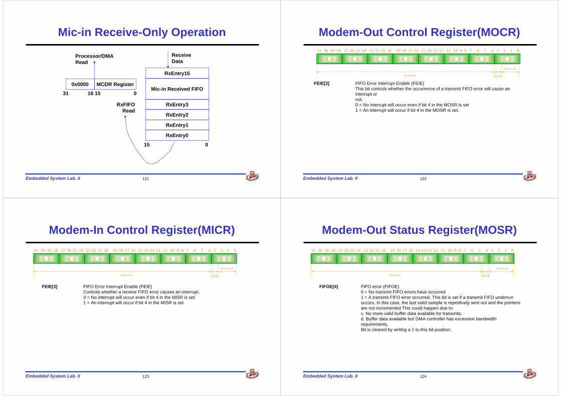
Embedded System Lab. II 121
Mic-in Receive-Only Operation
ReceiveData
RxEntry15
Mic-in Received FIFO
RxEntry3
RxEntry2
RxEntry1
RxEntry0
MCDR Register0x0000
Processor/DMARead
RxFIFORead
15 0
31 16 15 0
Embedded System Lab. II 122
Modem-Out Control Register(MOCR)
0 0 0 0 0 0 0 0 0 0 0 0 0 0 0 0 0 0 0 0 0 0 0 0 0 0 0 03 2 1 07 6 5 411 10 9 815 14 13 1219 18 17 1623 22 21 2027 26 25 2431 30 29 28
0 0 0 0
Reserved
Reserved
FEIE
FEIE[3] FIFO Error Interrupt Enable (FEIE)This bit controls whether the occurrence of a transmit FIFO error will cause an interrupt ornot.0 = No interrupt will occur even if bit 4 in the MOSR is set1 = An interrupt will occur if bit 4 in the MOSR is set.
Embedded System Lab. II 123
Modem-In Control Register(MICR)
0 0 0 0 0 0 0 0 0 0 0 0 0 0 0 0 0 0 0 0 0 0 0 0 0 0 0 03 2 1 07 6 5 411 10 9 815 14 13 1219 18 17 1623 22 21 2027 26 25 2431 30 29 28
0 0 0 0
Reserved
Reserved
FEIE
FEIE[3] FIFO Error Interrupt Enable (FEIE)Controls whether a receive FIFO error causes an interrupt.0 = No interrupt will occur even if bit 4 in the MISR is set1 = An interrupt will occur if bit 4 in the MISR is set.
Embedded System Lab. II 124
Modem-Out Status Register(MOSR)
Reserved
0 0 0 0 0 0 0 0 0 0 0 0 0 0 0 0 0 0 0 0 0 0 0 0 0 0 0 03 2 1 07 6 5 411 10 9 815 14 13 1219 18 17 1623 22 21 2027 26 25 2431 30 29 28
0 0 0 0
FIFOEReserved
FIFOE[4] FIFO error (FIFOE)0 = No transmit FIFO errors have occurred1 = A transmit FIFO error occurred. This bit is set if a transmit FIFO underrunoccurs. In this case, the last valid sample is repetitively sent out and the pointers are not incremented.This could happen due to:c. No more valid buffer data available for transmits.d. Buffer data available but DMA controller has excessive bandwidth requirements.Bit is cleared by writing a 1 to this bit position.

Embedded System Lab. II 125
Modem-In Status Register(MISR)
Reserved
0 0 0 0 0 0 0 0 0 0 0 0 0 0 0 0 0 0 0 0 0 0 0 0 0 0 0 0 0 0 0 0
FIFOEReserved
FIFOE[4] FIFO error (FIFOE)0 = No Receive FIFO error has occurred.1 = A receive FIFO error occurred. This bit is set if a receive FIFO overrun occurs. In thiscase, the FIFO pointers don't increment, the incoming data from the AC-link is notwritten into the FIFO and will be lost. This could happen due to DMA controller havingexcessive bandwidth requirements and hence not being able to flush out the ReceiveFIFO in time.Bit is cleared by writing a 1 to this bit position.
Embedded System Lab. II 126
Modem Data Register(MODR)
0 0 0 0 0 0 0 0 0 0 0 0 0 0 0 0 0 0 0 0 0 0 0 0 0 0 0 03 2 1 07 6 5 411 10 9 815 14 13 1219 18 17 1623 22 21 2027 26 25 2431 30 29 28
0 0 0 0
Reserved MODEM_DAT
MODEM_DAT[15:0] Modem data
Embedded System Lab. II 127
Modem Transmit and Receive Operation
TxEntry15
Modem TransmitFIFO
TxEntry3
TxEntry2
TxEntry1
TxEntry0
0x0000RxEntry15
Modem ReceiveFIFO
RxEntry3
RxEntry2
RxEntry1
RxEntry0
15 0
31 0
15 0
Transmit Data ReceiveDataProcessor/DMA
Write
Processor/DMARead
MODR Register16 15
Related Documents


![Udk] sound (sound cue)](https://static.cupdf.com/doc/110x72/5562fb97d8b42a62598b4b0a/udk-sound-sound-cue.jpg)