國 立 交 通 大 學 電機學院微電子奈米科技產業研發碩士班 碩 士 論 文 低溫複晶矽面板上之靜電放電耐受度研究 Investigation on Electrostatic Discharge (ESD) Robustness of Low Temperature Poly-Silicon (LTPS) Devices and Panels 研 究 生 : 莊介堯 指導教授 : 柯明道 教授 中華民國九十七年一月

Welcome message from author
This document is posted to help you gain knowledge. Please leave a comment to let me know what you think about it! Share it to your friends and learn new things together.
Transcript

國 立 交 通 大 學
電機學院微電子奈米科技產業研發碩士班
碩 士 論 文
低溫複晶矽面板上之靜電放電耐受度研究
Investigation on Electrostatic Discharge (ESD) Robustness of Low Temperature Poly-Silicon (LTPS)
Devices and Panels
研 究 生 莊介堯
指導教授 柯明道 教授
中華民國九十七年一月
低溫複晶矽面板上之靜電放電耐受度研究
Investigation on Electrostatic Discharge (ESD)
Robustness of Low Temperature Poly-Silicon
(LTPS) Devices and Panels
研 究 生 莊介堯 Student Jie-Yao Chuang
指導教授 柯明道 教授 Advisor Prof Ming-Dou Ker
國立交通大學
電機學院微電子奈米產業研發碩士班
碩士論文
A Thesis Submitted to Department of Electronics Engineering amp Institute of Electronics
College of Electrical and Computer Engineering National Chiao-Tung University
in Partial Fulfillment of the Requirements for the Degree of
Master in
Industrial Technology R amp D Master Program Jan 2008
Hsin-Chu Taiwan Republic of China
中華民國九十七年一月
低溫複晶矽面板上之靜電放電耐受度研究
學生 莊 介 堯 指導教授 柯 明 道 教授
國立交通大學
電機學院微電子奈米產業研發碩士班
摘要
低溫複晶矽 (low temperature poly-silicon LTPS) 薄膜電晶體 (thin-film
transistors TFT)已被視為一種材料廣泛地研究於可攜帶式系統產品中例如數位
相機行動電話個人數位助理(PDA) 筆記型電腦等等這是由於低溫複晶
矽薄膜電晶體的電子遷移率(electron mobility)約是傳統非晶矽(amorphous silicon)
薄膜電晶體的百倍大此外低溫複晶矽技術可藉由將驅動電路整合於顯示器之
週邊區域來達到輕薄巧小且高解析度的顯示器這樣的技術也將越來越適合於
系統面板(system-on-panelsystem-on-glass)應用之實現
靜電放電(electrostatic discharge ESD)在積體電路(integrated circuits ICs)中
是一個產品可靠度上的重要問題當靜電放電發生於平面顯示器上時常會造成
產品生產良率的降低所以如何防制靜電放電的發生在平面顯示器的生產上更
是一重要課題
基於此本論文詳細研究了在 3μm 低溫複晶矽薄膜製程下之靜電放電防護
元件並藉由在元件上變化不同的佈局參數使用傳統的傳輸線脈衝(transmission
line pulsing TLP)產生系統和長脈衝-傳輸線脈衝系統(long-pulse transmission
line pulsing system LP-TLP)觀測元件在靜電轟擊下之電性特徵本論文利用傳統
型傳輸線脈衝系統及長脈衝-傳輸線脈衝系統量測到之待測薄膜元件之二次崩
潰特性(secondary breakdown characteristic)點來說明及探討元件佈局結構之靜電
耐受力的影響並憑藉量測不同參數和佈局尺寸的薄膜元件可歸納出應用於液
晶面板上的靜電放電防護設計之最佳化方式
在全系統面板應用電路設計組裝中因隨著全面板的生產過程之各模組的組
裝待組裝物設備或是人員之間所產生的面板上靜電放電以致於越來越嚴重
良率下降問題故本論文藉由利用於觀測面板上之靜電放電實際事件來進一步
分析電路元件遭受人體放電模式(Human Body Model HBM)機器放電模式
(Machine Model MM)及模組儲存電荷模式(Charged Device Model CDM) 之元件
故障點分析
-iii-
Investigation on Electrostatic Discharge (ESD)
Robustness of Low Temperature Poly-Silicon
(LTPS) Devices and Panels
Student Jie-Yao Chuang Advisor Prof Ming-Dou Ker
Industrial Technology R amp D Master Program of Electrical and Computer Engineering College
National Chiao-Tung University
ABSTRACT
Low temperature poly-silicon (LTPS) thin-film transistors (TFTs) have been
widely investigated as a material for portable systems such as digital camera mobile
phone personal digital assistants (PDAs) notebook and so on because the electron
mobility of LTPS TFTs is about 100 times larger than that of the conventional
amorphous silicon TFTs Furthermore LTPS technology can achieve slim compact
and high-resolution display by integrating the driving circuits on peripheral area of
display This technology will also become more suitable for realization of
system-on-panelsystem-on-glass (SoPSoG) applications
The electrostatic discharge (ESD) is one of the major reliability concerns in
integrated circuits (ICs) and the most critical issue on the flat display panel to reduce
the production yield
In order to design high performance ESD protection device and realize the
-iv-
secondary breakdown characteristic of ESD protection devices in 3-μm LTPS
technology the turn-on characteristics of those devices must be measured and
analyzed by using the long-pulse transmission line pulsing (LP-TLP) system and
traditional 100-ns transmission line pulsing (TLP) system in this thesis From the
investigation of layout dependence on ESD protection devices with finger-type
layout the turn-on mechanisms of ESD protection devices can be clearly understood
to optimize the layout rules for the device dimensions the layout style and the
layout spacing of those devices
More ESD problems on panel are growing importance due to many industrial
cases where such discharges have resulted in numerous device failures of
electrostatic origin for the assembliesmodules The goal of this thesis is to analyze
and explain the integrated circuit of whole-panel under LTPS process the effects that
are seen on display panel when they are subjected to the charged device model
(CDM) versus human body model (HBM) and machine model (MM) ESD events
-v-
誌謝
來到交通大學最難得的莫過於能受到柯明道教授的指導柯教授讓我瞭解到
專業知識固然重要但如何運用來解決問題才最重要另外柯教授對於凡事積極
正面的態度對我於學校中做實驗的方向受益良多讓我從一個一開始什麼都不
懂的菜鳥歷經多次的摸索與跌倒開始對做研究有個比較清晰的概念而在每
次的討論除了專業上的教導讓我收穫更多的則是柯教授對生命的熱忱對人
事物諸多正面且正確的分析與見解著實讓我受益匪淺讓我不論在未來的工
作或生活上能夠有另外一種層次的思考來面對所遭遇的種種是我在這碩士班二
年的日子以來讓我最感深刻然而現實生活中的研究正如同現實生活中的人
生在實驗學習過程中往往會發生許多料想不到的意外和很多很麻煩卻又不得
不去做的事物在繁雜瑣碎的意外事我們無法去避免而我們唯一能努力的
無非是仔細地思考用心地計畫未來必須做的每一步及規劃並且努力地去完成
它突破它至於成功與否就虛心接受因為自己已經盡了最大的努力而問
心無愧教授的苦口婆心到最後才真正的有所體悟而柯教授在細心且耐心的
指導下學生為此由衷地感謝教授對學生的付出 在這段求學實驗的過程中『友達光電股份有限公司』給予我許多的研究的
資源與幫助使我的靜電放電防護元件能夠順利完成在此特別感謝李純懷經
理郭俊宏副理等諸位長官以及『工研院系統晶片技術發展中心』的陳世宏學長
和『晶焱科技股份有限公司』的曾當貴林昆賢陳子平李健銘等學長們在
實驗與量測設備上所給予我的幫忙與專業上的指導 此外我也要感謝『奈米晶片與系統實驗室』的陳榮昇顏承正陳穩義
張瑋仁蕭淵文陳志豪賴泰翔王資閔王暢資李宇軒廖期聖陸亭州
陳紹岐蔡佳琪翁怡歆等學長姐以和學弟們以及『電子材料及電子構裝實驗
室諸位實驗室』的鄧至剛學長等在各方面給予我許多幫助及指導使我能順利完
成碩士論文更感謝『奈米晶片與系統實驗室』及助理卓慧貞小姐給予我在研究
上的資源及行政上的幫助讓我完成學業我在撰寫本論文的過程中雖力求嚴
謹然誤謬之處在所難免尚祈各位讀者賜予寶貴意見使本論文能更加完善 最後我要謝謝我的父母和家人及女友給予我一切的協助使我無後顧之
憂並且在我失去信心時給我支持與鼓勵而從未對我失去過信心這一直是我
精神上最大的支柱 還要感謝很多人不可勝數在此一併謝過我不會讓你們失望的
莊介堯
僅誌於竹塹交大
九十七年一月
-vi-
CONTENTS
ABSTRACT (CHINESE) i
ABSTRACT (ENGLISH)iii
ACKNOWLEDGEMENT v
FIGURE CAPTIONS viii
TABLE CAPTIONS xii
Chapter 1 Introduction 1
11 MOTIVATION 1 12 THESIS ORGANIZATION 2
Chapter 2 Background Knowledge of Thin-Film Transistor
Liquid Crystal Displays and ESD 4
21 LCD INDUSTRY AND LTPS TECHNOLOGY4 211 System-on-PaneSystem-on-GlasslDisplays 5 212 The Advantages of the SoPSoG LTPS TFT-LCD Displays 6
22 GENERAL INTRODUCTION TO ESD 7 221 Human Body Model (HBM) 8 222 Machine Model (MM) 8 223 Charged Device Model (CDM)9
23 ESD TEST METHODS 9 231 ESD Test on IO Pins9 232 Pin to Pin ESD Test10 233 VDD-to-VSS ESD Test11
24 ESD PROTECTION NETWORK11 25 ESD PROTECTION DEVICES IN MODERN CMOS ICS 12
Chapter 3 Wafer-Level Transmission Line Pulsing (WL-TLP)
System 27
31 100-ns TRANSMISSION LINE PULSING (TLP) SYSTEM 27
-vii-
32 Long-Pulse Transmission Line Pulsing (LP-TLP) System28 321 Verification on conventional N-type TFT Under 300-ns
Long-Pulse Transmission Line Pulsing Stress 30
Chapter 4 Dependence of Layout Parameters on ESD
Robustness devices in 3-μm LTPS Process 36
41 LTPS N-TFTP-TFT ESD PROTECTION DEVICES36 411 Channel Width37 412 Channel Length 38 413 Fixed WL Radio 40 414 LDD Length 41
42 LTPS P+-Nminus-N+P+-i-N+ DIODES42 421 Measurement Result of the LTPS Diodes42
43 THIN-FILM POLY SILICON-CONTROLLED-RECTIFIER (SCR) DEVICE 44
Chapter 5 The Comparison of Failure Signatures of LTPS
Display Panel under HBM MM and CDM ESD
Stresses 67
51 INTRODUCTION 67 52 ESD TESTER MEASUREMENT SETUP68 53 ESD EVENT EXPERIMENTAL RESULTS 69
531 HBM and MM Experimental Results 69 532 CBM Experimental Results 70
Chapter 6 Conclusion and Future Works 76
61 CONCLUSION76 62 FUTRUE WORKS77
REFERENCES 78
VITA
-viii-
FIGURE CAPTIONS
Fig 21 System integration roadmap of LTPS TFT-LCD16 Fig 22 Basic concept of pixel memory technology 16 Fig 23 (a) The schematic illustration of the ldquosheet computerrdquo concept and (b) a CPU
with an instruction set of 1-4 bytes and an 8b data bus on glass substrate17 Fig 24 The roadmap of LTPS technologies leading toward the realization of sheet
computers 17 Fig 25 Schematic cross-section view of the structure of a LTPS complementary metal
oxide semiconductor (CMOS) LDD = lightly doped drain 18 Fig 26 (a) Comparison of an amorphous silicon TFT-LCD module and (b) a
low-temperature polycrystalline silicon TFT-LCD module 18 Fig 27 The comparison of new SoPSoG technology product and conventional
product The new 38rdquo SoP LTPS TFT-LCD panel has been manufactured by SONY corp in 2002 19
Fig 28 The equivalent circuit of the human body model ESD event19 Fig 29 Definition of the HBM pulse decay time (td)20 Fig 210 The equivalent circuit of the machine model ESD event20 Fig 211 The current waveform of a 400-V MM ESD stress discharging through a
short wire21 Fig 212 The equivalent circuit of the charge device model ESD event 21 Fig 213 Field induced CDM simulator22 Fig 214 Comparison on waveforms of a 2-kV HBM ESD stress 200-V MM ESD
stress and a 1-kV CDM ESD stress22 Fig 215 (a) PS-mode (b) NS-mode (c) PD-mode and (d) ND-mode ESD test on
IO pins23 Fig 216 (a) Positive mode (b) Negative-mode pin-to-pin ESD test23 Fig 217 (a) Positive mode (b) Negative-mode VDD-to-VSS ESD test24 Fig 218 The ESD current discharging paths (path 1 and path 2) during the pin-to-pin
ESD stress condition 24 Fig 219 (a) Device cross-sectional view (b) simplified structural illustration (c)
equivalent circuit and (d) typical I-V characteristic of SCR device25 Fig 220 (a) Device cross-sectional view (b) simplified structural illustration and (c)
equivalent circuit of another SCR device26 Fig 31 The configuration of 100-ns TLP system applied for LTPS thin-film devices
31 Fig 32 The LTPS thin-film device is measured by TLP system 31
-ix-
Fig 33 The TLP waveforms on LTPS devices are monitored by the oscilloscope (a) before and (b) after the thin-film device fails 32
Fig 34 The configuration of LP-TLP system applied for LTPS thin-film devices 33 Fig 35 The actual measurement setup for the LP-TLP test33 Fig 36 The 300-ns LP-TLP measured I-V characteristic of the N-type TFT device
34 Fig 37 (a)-(d) The measured time-domain I-V waveforms of the N-type TFT device
at the corresponding points marked in Fig 36 35 Fig 41 The layout top views of (a) the conventional N-type TFT device and (b) the
conventional P-type TFT device in LTPS technology47 Fig 42 (a) The top views of the diode-connected N-TFT device and (b) the layout
top views of the diode-connected N-TFT device in LTPS technology 48 Fig 43 The TLP-measured I-V curves of (a) the diode-connected N-TFT devices
and (b) the diode-connected P-TFT devices with different channel widths under forward TLP stress 49
Fig 44 The dependence of the It2 and the fresh leakage currents of (a) the diode-connected N-TFT devices and (b) the diode-connected P-TFT devices on different channel widths 50
Fig 45 The dependence of the It2 of (a) the diode-connected N-TFT devices and (b) the diode-connected P-TFT devices on different channel widths under forward 100-ns TLP and 300-ns 500-ns or 1000-ns LP-TLP stress51
Fig 46 The TLP-measured I-V curves of (a) the diode-connected N-TFT devices and (b) the diode-connected P-TFT devices with different channel lengths under forward TLP stress 52
Fig 47 The dependence of the It2 and the fresh leakage currents of (a) the diode-connected N-TFT devices and (b) the diode-connected P-TFT devices on different channel lengths 53
Fig 48 The dependence of the It2 of (a) the diode-connected N-TFT devices and (b) the diode-connected P-TFT devices on different channel lengths under forward 100-ns TLP and 300-ns 500-ns or 1000-ns LP-TLP stress54
Fig 49 The TLP-measured I-V curves of (a) the diode-connected N-TFT devices and (b) the diode-connected P-TFT devices with fixed radio of WL=100 under forward TLP stress 55
Fig 410 The dependence of the It2 and the fresh leakage currents of (a) the diode-connected N-TFT devices and (b) the diode-connected P-TFT devices on fixed WL=100 ratio 56
Fig 411 The dependence of the It2 of (a) the diode-connected N-TFT devices and (b) the diode-connected P-TFT devices on fixed radio of WL=100 under
-x-
forward 100-ns TLP and 300-ns 500-ns or 1000-ns LP-TLP stress57 Fig 412 The TLP-measured I-V curves of the diode-connected N-TFT devices
with different LDD lengths under forward TLP stress58 Fig 413 The dependence of the It2 and the fresh leakage currents of the
diode-connected N-TFT devices on different LDD lengths under forward 100-ns TLP stress 58
Fig 414 Fig 410 The simulation result of the diode-connected N-TFT device with (a) LDD=125 μm (b) LDD=325 μm under forward ESD-like voltage stress59
Fig 415 The dependence of the It2 of the diode-connected N-TFT devices on different LDD lengths under forward 100-ns TLP and 300-ns 500-ns or 1000-ns LP-TLP stress 60
Fig 416 The layout top views of three LTPS diodes with (a) Nminus and (b) intrinsic ion doping in the center region61
Fig 417 The TLP-measured I-V curves of two LTPS diodes with a dimension (WS) of 500 μm5 μm under forward-biased condition 62
Fig 418 The TLP-measured I-V curves of the P+-Nminus-N+ LTPS diodes under forward TLP stress 62
Fig 419 The TLP-measured I-V curves of the P+-i-N+ LTPS diodes under forward TLP stress 63
Fig 420 The dependence of the It2 and the fresh leakage currents of the P+-i-N+ LTPS diodes 63
Fig 421 The dependence of the It2 and the fresh leakage currents of the P+-Nminus-N+ LTPS diodes 64
Fig 422 The relations of It2 and the spacing S of these two different LTPS diodes under forward TLP stresses 64
Fig 423 The dependence of the It2 of (a) the P+-Nminus-N+ LTPS diodes (b) the P+-Nminus-N+ LTPS diodes with different spacing under forward 100-ns TLP and 300-ns 500-ns or 1000-ns LP-TLP stress65
Fig 424 The cross-section of the thin-film poly silicon-controlled rectifier structure under the LTPS process 66
Fig 425 The measurement setup and measurement result of poly-SCR under the LTPS process66
Fig 51 The 1-to-6 switch circuit of basic integrated circuit under LTPS process71 Fig 52 The measurement setup for the HBM and MM ESD events test 71 Fig 53 The measurement setup for the CBM ESD events test 72 Fig 54 The actual measurement setup for the CBM ESD events test72 Fig 55 The impact of 1-to-6 switch circuit to the discharging paths of ESD current
-xi-
under the specified pin-to-pin ESD stress 73 Fig 56 The top-view of failure site after (a) HBM 350V ESD stress and (b) MM
150V ESD stress73 Fig 57 The impact of 1-to-6 switch circuit to the discharging paths of ESD current
from device to ground 74 Fig 58 Measurement 800-V field-induced CDM ESD discharge current waveform
74 Fig 59 The top-view of failure site after CDM 800V ESD stress ESD stress 75 Fig 510 The impact of 1-to-6 switch circuit to the discharging paths of ESD current
from device to ground 75 Fig 511 The top-view of failure site after CDM 800V ESD stress ESD stress 75
-xii-
TABLE CAPTIONS
Table 41 The descriptions for different layout parameters 46
-1-
Chapter 1
Introduction
11 MOTIVATION
Low temperature poly-silicon (LTPS) thin-film transistors (TFTs) have been
widely used in active matrix liquid crystal display (AMLCD) because their electron
mobility can be 100 times faster than that of the conventional amorphous silicon
(a-SiH) TFTs [1] Many small-size to mid-size AMLCDs fabricated by LTPS
technology have been used in mobile phone digital camera personal digital assistants
(PDAs) notebook and so on The state-of-the-art design efforts focus on realization
of system-on-panel system-on-glass (SoPSoG) application [2] [3] to integrate more
control and driver circuits on the glass substrate
The electrostatic discharge (ESD) is one of the major reliability concerns in
integrated circuits (ICs) [4] and it is also the most critical issue on the flat display
panel to reduce the production yield [5] When the large glass panel is delivered or
assembled in the factory the insulator material or the process machines could
accumulate considerable static charges by triboelectric and field-induced charging
Since the fabricated material used for thin-film devices has a low thermal conductivity
the heat generated by ESD current cannot be efficiently dissipated in contract to the
CMOS devices in deep substrate with a low thermal resistance At the secondary
breakdown point the stressed device reaches a critical temperature by ESD to initiate
thermal runaway [6] With joule heating consideration [7] the ESD reliability of
LTPS thin-film devices becomes more serious when the design rules are shrunk to
-2-
make more devices and circuits integrated on LCD panel
Compared to silicon-based CMOS technology a few papers were studied on
thin-film devices under ESD-stress condition [8-13] Under the system level ESD test
[14] the ESD reliability of panel was tested by an ESD gun with a voltage level of
several kV [8] At the device level a-Si TFTs under machine-model (MM) ESD test
[15] and under transmission line pulsing (TLP) test [16] were studied [8-11] The
transmission line pulsing (TLP) system with a 100-ns current pulse was used to
investigate ESD degradation on LTPS TFTs [12] [13] The device dimension of TFTs
studied in [8-13] was so small that they could not sustain high ESD current and failed
as long as they were turned on Therefore only the failure result on TFTs after
different over-voltage stress conditions is demonstrated No high-current
characteristic of TFT under ESD-stress condition was presented in those published
papers
In order to design high performance ESD protection device and realize the
secondary breakdown characteristic of ESD protection devices in 3-μm LTPS
technology the turn-on characteristics of those devices must be measured and
analyzed by using the long-pulse transmission line pulsing (LP-TLP) system and
traditional 100-ns TLP system in this thesis From the investigation of layout
dependence on ESD protection devices with finger-type layout the turn-on
mechanisms of ESD protection devices can be clearly understood to optimize the
layout rules for the device dimensions the layout style and the layout spacing of
those devices
12 THESIS ORGANIZATION
The chapter 2 of this thesis introduces some background knowledge of thin-film
-3-
transistor liquid crystal displays liquid crystal display structure in TFT-LCD panel
ESD events ESD test methods and general ESD protection techniques
In the chapter 3 and chapter 4 this thesis introduces traditional 100 ns
transmission line pulsing (TLP) system and long-pulse transmission line pulsing
(LP-TLP) system is set up The LP-TLP system with three kinds of long pulse widths
(300 ns 500 ns and 1000 ns) is evidently different from the with a short pulse width
of 100 ns From the experimental results of ESD protection under LTPS process can
be clearly understood to optimize the layout rules for the device dimensions the
layout style and the layout spacing of those devices
Chapter 5 is to compare and contrast the effects that are seen on display panel
when they are subjected to the CBM versus HBM and MM ESD events
Chapter 6 is the conclusions of this thesis and the future works on this topic
-4-
Chapter 2
Background Knowledge of Thin-Film Transistor
Liquid Crystal Displays and ESD
21 LCD INDUSTRY AND LTPS TECHNOLOGY [17] [18]
The liquid-crystal display (LCD) industry has shown rapid growth in five market
areas namely notebook computers monitors mobile equipment mobile telephones
and televisions For high-speed communication networks the emerging portable
information tools are expected to grow in following on the rapid development of
display technologies Thus the development of higher specification is demanded for
LCD as an information display device Moreover the continual growth in network
infrastructures will drive the demand for displays in mobile applications and flat
panels for computer monitors and TVs The specifications of these applications will
require high-quality displays that are inexpensive energy-efficient lightweight and
thin
Amorphous silicon (a-Si) thin-film transistors (TFTs) are widely used for
flat-panel displays However the low field-effect mobility (ability to conduct current)
of a-Si TFTs allows their application only as pixel switching devices they cannot be
used for complex circuits In contrast the high driving ability of polycrystalline Si
(p-Si) TFTs allows the integration of various circuits such as display drivers
Eliminating LSI (large-scale integration) chips for display drivers will decrease the
cost and thickness of displays for various applications There are high-temperature
-5-
and low-temperature poly-Si TFTs defined by the maximum process temperature they
can withstand The process temperature for high-temperature poly-Si can be as high
as 900degC Hence expensive quartz substrates are required and the profitable substrate
size is limited to around 6 in (diagonal) Typical applications are limited to small
displays The process temperature for low-temperature poly-Si (LTPS) TFTs on the
other hand is less than 600degC which would allow the use of low-cost glass substrates
This makes possible direct-view large-area displaysmdashfor example UXGA (ultra
extended graphics array) monitors of up to 151 in (diagonal) with a resolution of
1600 x 1200 pixels For this reason LTPS technology has been applied successfully to
not only small-sized displays but also medium- and large-screen products
211 System-on-PanelSystem-on-glass Displays
LTPS TFT-LCD technology has some features of system integration within a
display It can make a compact high reliable high resolution display Because of this
property LTPS TFT-LCD technology is widely used for mobile displays Fig 21
shows the system integration roadmap of LTPS TFT-LCD [19] [20]
System-on-panel (SoP) displays are value-added displays with various functional
circuits including static random access memory (SRAM) in each pixel integrated on
the glass substrate [19] Fig 22 shows the basic concept of pixel memory technology
When SRAMs and a liquid crystal AC driver are integrated in a pixel area under the
reflective pixel electrode the LCD is driven by only the pixel circuit to display a still
image It means that no charging current to the data line for a still image This result is
more suitable for ultra low power operation Eventually it may be possible to
combine the keyboard CPU memory and display into a single ldquosheet computerrdquo The
schematic illustration of the ldquosheet computerrdquo concept and a CPU with an instruction
set of 1-4 bytes and an 8b data bus on glass substrate are shown in Fig 23
-6-
respectively [17] [21] Fig 24 shows the roadmap of LTPS technologies leading
toward the realization of sheet computers Finally all of the necessary function will be
integrated in LTPS TFT-LCD Although the level of LTPS is as almost the same as the
level of the crystal Si of 20 years ago actual operation of 50MHz with 1μm design
will be realized near future [22]
212 The Advantages of the SoPSoG LTPS TFT-LCD Displays
The distinctive feature of the LTPS TFT-LCD is the elimination of TAB-ICs
(integrated circuits formed by means of an interconnect technology known as
tape-automated bonding) LTPS TFTs can be used to manufacture complementary
metal oxide semiconductors (CMOSs) in the same way as in crystalline silicon metal
oxide semiconductor field-effect transistors (MOSFETs) Fig 25 shows the cross
sectional structure of a LTPS TFT CMOS In the LTPS process a buffer oxide and an
α-SiH film were deposited on glass substrate by plasma enhanced chemical vapor
deposition (PECVD) system and then the XeCl excimer laser was used to crystallize
this film [23] The thickness of α-Si film deposited in this work is about 50 nm After
active islands were defined the ion doping process was carried out to the N+ regions
Following double gate insulator films SiOX and SiNX were deposited by PECVD
system The gate metal Mo was deposited and then patterned Subsequently the
Nminus and P+ ion dopings were implanted in the lightly doped drain (LDD) region and
the P+ region of LTPS TFT device on panel respectively Here the Nminus doping is a
self-aligned process without extra mask All ion doping processes were completed the
doping activation was performed by rapid thermal annealing (RTA) After the
inter-metal dielectric (IMD) layer was deposited the contact holes and the metal pads
were formed for interconnection as shown in Fig 25 Moreover hydrogenation was
used to improve the device performance [24] Finally all LTPS thin-film devices
-7-
including diodes and transistors were finished after their contact holes and metal pads
formation
For a-Si TFT-LCDs TAB-ICs are connected to the left and bottom side as the Y
driver and the X driver respectively Integration of the Y and X drivers with LTPS
TFTs requires PCB (printed circuit board) connections on the bottom of the panel only
The PCB connection pads are thus reduced to one-twentieth the size of those in a-Si
TFT-LCDs The most common failure mechanism of TFT-LCDs disconnection of the
TAB-ICs is therefore decreased significantly For this reason the reliability and yield
of the manufacturing can be improved Decreasing the number of TAB-IC
connections also achieves a high-resolution display because the TAB-IC pitch
(spacing between connection pads) limits display resolution to 130 ppi (pixels per
inch) A higher resolution of up to 200 ppi can be achieved by LTPS TFT-LCDs
Therefore the SoP technology can effectively relax the limit on the pitch between
connection terminals to be suitable for high-resolution display Furthermore
eliminating TAB-ICs allows more flexibility in the design of the display system
because three sides of the display are now free of TAB-ICs [17] Fig 26 shows a
comparison of a-Si and LTPS TFT-LCD modules The 38rdquo SoP LTPS TFT-LCD
panel has been manufactured successfully and it is shown in Fig 27
22 GENERAL INTRODUCTION TO ESD
ESD is a phenomenon caused by the discharging of electrostatic charges on IC
pins It can be arose from events such as a physical contact of a human body and an
IC products touch of manufacturing machines and wafers or discharge of
secondhand induced electrical field on an IC chips Because ESD can be brought
about by different origins it can be classified to human-body model (HBM)
-8-
machine-model (MM) and charged-device model (CDM) according to different
discharging methods and sources of electrostatic charges
221 Human-Body Model (HBM)
HBM is a typical ESD event arose from the contact of an electrified human body
and an IC product The ESD static charges are initially stored in the human body and
then transfer into the IC when the human body touches the IC The equivalent circuit
for HBM ESD event is shown in Fig 28 [25] where the 15-kΩ resistor and the
100-pF capacitor represent the equivalent parasitic resistor and capacitor of a human
body The DUT in Fig 28 represents the device under test The HBM circuit is
designed to eliminate the weak protection designs and susceptible devices of the DUT
Fig 29 shows the specifications of a HBM ESD waveform generated by the ESD
HBM tester to a short wire [25] Generally commercial ICs are requested to pass
2-kV HBM ESD stress at least which can generate ESD current with a peak value of
~13Amp and a rise time of ~10ns
222 Machine Model (MM)
The equivalent circuit diagram of MM ESD event is shown in Fig 210 [26]
where there is no equivalent resistor on the equivalent discharging path because the
MM ESD stress is to replicate the ESD event arose from the contact of a machine and
a semiconductor device Fig 211 shows the waveform of a 400-V MM ESD pulse
generated by the MM ESD tester [26] A commercial IC product is generally required
to pass at least 200-V MM ESD stress which can generate an ESD current with a
peak value of ~35Amp and a rise time of ~10ns The MM ESD level of a
semiconductor device is generally 8~12 times smaller than its HBM ESD level for the
faster rise time and voltage resonance of a MM ESD pulse
-9-
223 Charged-Device Model (CDM)
The equivalent circuit for CDM ESD event is shown in Fig 213 The CDM
ESD event is caused by the discharging of electrostatic charges initially stored in the
body of a floating IC Most of the CDM charges are stored in the body (the
p-substrate) of a CMOS IC at first by triboelectric and field-induced charging as
shows in Fig 213 When one or more pins of this charged IC is touched by an
external grounded object charges in the p-substrate will be discharged from the IC
inside to the grounded pin outside There is no standard equivalent parasitic capacitor
for the CDM ESD stress because different dimension of chips different form and size
of packages result in different values of the parasitic capacitor of IC chips A
commercial IC is generally requested to pass at least 1-kV CDM ESD stress which
can generate an ESD current with peak current value as high as ~15A within a rise
time less than 200ps [27] Fig 214 compares the waveforms of a 2-kV HBM ESD
stress a 200-V MM ESD stress and a 1-kV CDM ESD stress which has 4-pF
equivalent capacitor of the device under test
23 ESD TEST METHODS
Since electrical charges in natural environment can be either positive or negative
ESD tests have positive and negative modes too Moreover since ESD event can
occur on inputoutput (IO) pins power pins or between different IO pins of an IC
chip ESD test methods have pin combinations as follows
231 ESD Test on IO Pins
For every IO pin of an IC chip under the human-body model and the
machine-mode ESD tests there are four test modes as illustrated through Fig 215(a)
-10-
to 215(d) [28] [29]
(1) PS mode
Positive ESD voltage applied to the tested IO pin with VSS pins relatively
grounded VDD pins and all other pins are kept floating during the test as shown in
Fig 215(a)
(2) NS mode
Negative ESD voltage applied to the tested IO pin with VSS pins relatively
grounded VDD pins and all other pins are kept floating during the test as shown in
Fig 215(b)
(3) PD mode
Positive ESD voltage applied to the tested IO pin with VDD pins relatively
grounded VSS pins and all other pins are kept floating during the test as shown in
Fig 215(c)
(4) ND mode
Negative ESD voltage applied to the tested IO pin with VDD pins relatively
grounded VSS pins and all other pins are kept floating during the test as shown in
Fig 215(d)
232 Pin-to-Pin ESD Test
Besides the ESD test on IO pins ESD events can happen on one of the IO
pins with another IO pin relatively grounded If the two IO pins are not correlated to
each other in circuitry ESD current will first be diverted from the stressed IO pin to
the VDD or VSS power line and then be discharged to the grounded IO pin
Therefore during the pin-to-pin ESD tests power pins of the tested chip are kept
floating However it could take a long testing period if every IO pin of an IC chip is
tested one by one To shorten the testing period positive or negative ESD voltage is
-11-
applied on the tested IO pin with all other IO pins relatively grounded as illustrated
in Fig 216(a) and Fig 216(b)
233 ESD Test on Power Pins (VDD-to-VSS ESD Test)
The ESD test on power pins or the VDD-to-VSS ESD stresses simulate ESD
events that happen between two power pins A positive or a negative ESD voltage
during the VDD-to-VSS ESD stress is applied to the VDD power pin of the device
under test while the VSS power pin is relatively grounded as shown in Fig 217
24 ESD PROTECTION NETWORK
The various ESD test methods suggest that ESD events can damage not only IO
circuits but also internal circuits especially under the pin-to-pin and the VDD-to-VSS
ESD stresses These two ESD test modes often lead to some unexpected ESD current
through the IO ESD protection circuits and the power lines into the internal circuits
and result in ESD damage on the internal circuits [30] [31] Therefore to effectively
protect chips from the ESD damage ESD protection designs are required on both IO
circuits and between the power lines Fig 218 illustrates the impact of the power-rail
ESD clamp circuit to the discharging paths of ESD current (IESD) under the specified
pin-to-pin ESD stress When a positive ESD voltage is applied to some input pin (IP)
with some output pin (OP) grounded and the VDD and VSS pins floating some ESD
current will be diverted from the input pin to the floating VDD power line and then to
the internal circuits (path 1) if the power-rail ESD protection circuit is not designed
in Fig 218 The ESD protection circuits at the IO pins are often designed strong
enough to discharge the huge ESD current but the internal circuits are easily damaged
to cause unexpected damages on internal circuits If an effective ESD clamp circuit is
-12-
added between the VDD and VSS power lines the ESD current can be discharged
through the power-rail ESD clamp circuit (path 2) instead of the internal circuits (path
1) Therefore the internal circuits can be safely protected against such unexpected
ESD damage Moreover the power-rail ESD clamp circuit can also protect the whole
chip against the VDD-to-VSS ESD testing mode Thus an effective power-rail ESD
clamp circuit between the VDD and VSS power lines is necessary for the whole-chip
ESD protection [31]
Therefore a whole-chip ESD protection network should include not only ESD
protection circuits at the IO pins but also power-rail ESD clamp circuits The
whole-chip ESD protection network appropriate ESD protection devices and
effective techniques to trigger the ESD protection devices are the keys for IC products
to carry off high ESD robustness
25 ESD PROTECTION DEVICES IN MODERN CMOS ICS
To protect ICs from being damaged by ESD current it is important to choose
appropriate ESD protection device under different ESD protection networks and
different system specifications In modern CMOS ICs ESD protection devices in
common use include
(1) P-N Junction Diode
A diode device has low forward cut-in voltage (~06 V) and high reverse
breakdown voltage which can be higher than 10 V Both forward diodes in series and
a reverse diode can serve as the ESD protection circuit to protect internal circuits from
being damaged by ESD current When a reverse diode is used as an ESD protection
device its reverse breakdown voltage is required to be smaller than the gate oxide
-13-
breakdown voltage of MOS devices so that ESD current can be discharged to ground
through the reverse diode without damaging the gate oxide of internal circuits A
larger device dimension of the ESD protection diode is also required when it is
operated in reverse mode because the high reverse breakdown voltage generates huge
heat to be dissipated during ESD stresses
(2) MOS Device (NMOS or PMOS)
MOS devices are the most common ESD protection devices in CMOS ICs The
n+ drain junction p-substrate and the n+ source junction of an NMOS device construct
a parasitic n-p-n bipolar junction transistor When the high ESD stress voltage occurs
the parasitic n-p-n bipolar junction transistor inherent in NMOS device structure can
be turned-on to carry the huge ESD current and to clamp down the ESD voltage to
protect gate oxide of internal circuits As a result the I-V characteristic curve of an
NMOS device under ESD stresses often has the snapback phenomenon due to the turn
on of the parasitic n-p-n bipolar The p+ drain junction n-well substrate and p+ source
junction of PMOS device form a parasitic p-n-p bipolar junction transistor inherent in
its device structure PMOS devices in CMOS ICs can therefore serve as an ESD
protection device However the beta gain of p-n-p bipolar junction transistor in
CMOS process is much smaller than that of n-p-n bipolar junction transistor I-V
characteristic curves of PMOS under ESD stresses have no or weak snapback
phenomenon
(3) Silicon Controlled Rectifier (SCR)
The SCR device can sustain a much higher ESD level within a smaller layout
area in CMOS ICs so it has been used to protect the internal circuits against ESD
damage for a long time The SCR device is a component with p-n-p-n structure it
-14-
consists of P-plus (P+) diffusion N-well (NW) P-well (PW) and N-plus (N+)
diffusion in CMOS ICs process as shown in Fig 219(a) and Fig 219(b) A SCR
device has a p-n-p and an n-p-n bipolar junction transistor with regenerative feedback
to each other so that SCR device can clamp the ESD voltage at a relatively low
holding voltage (~12 V) compared to that of NMOS devices A typical I-V
characteristic of the SCR device operation and equivalent circuit is shown in Fig
219(c) and Fig 219(d) Therefore SCR device can achieve high ESD protection
level within small layout area due to its low holding voltage However a SCR device
has drawbacks such as high turn-on voltage low turn-on speed and latch-up issue To
sum up different ESD protection devices have respective advantages and
disadvantages The SCR device is important to pick the appropriate device as an ESD
protection element according to different power-supply voltages ESD protection
networks system specifications and device characteristics Therefore The SCR
device can sustain a much higher ESD level within a smaller layout area in CMOS
ICs so it has been used to protect the internal circuits against ESD damage for a long
time [32] [33]
A slight modification on the SCR structure gives it faster turn-on efficiency and
the ability to be triggered on by an external trigger circuit as shown in Fig 220(a) to
Fig 220(c) [33] Once an additional p-plus diffusion layer is inserted right in between
the p-well and n-well layer the SCR can have a much lower avalanche breakdown
voltage since the p-plus diffusion doping concentration is higher than that in the
p-well Therefore the switching voltage is reduced from the NW-PW junction
avalanche breakdown voltage to the NW-P+ junction breakdown voltage The SCR
can then be turned on by a much lower positive anode voltage Further if a current is
purposefully injected into this p-plus layer this current serve as the base current of the
lateral n-p-n transistor and thus the lateral n-p-n transistor can be triggered on
-15-
Consequently the positive-feedback regenerative mechanism of latchup is initiated
and the SCR device will be soon turned on
-16-
Fig 21 System integration roadmap of LTPS TFT-LCD
Fig 22 Basic concept of pixel memory technology
-17-
Fig 23 (a) The schematic illustration of the ldquosheet computerrdquo concept and (b) a CPU
with an instruction set of 1-4 bytes and an 8b data bus on glass substrate
Fig 24 The roadmap of LTPS technologies leading toward the realization of sheet
computers
(a) (b)
-18-
Fig 25 Schematic cross-section view of the structure of a LTPS complementary
metal oxide semiconductor (CMOS) LDD = lightly doped drain
(a) (b)
Fig 26 (a) Comparison of an amorphous silicon TFT-LCD module and (b) a
low-temperature polycrystalline silicon TFT-LCD module
-19-
Fig 27 The comparison of new SoPSoG technology product and conventional
product The new 38rdquo SoP LTPS TFT-LCD panel has been manufactured by SONY
corp in 2002
Fig 28 The equivalent circuit of the human body model ESD event
-20-
Fig 29 Definition of the HBM pulse decay time (td)
Fig 210 The equivalent circuit of the machine model ESD event
-21-
Fig 211 The current waveform of a 400-V MM ESD stress discharging through a
short wire
Fig 212 The equivalent circuit of the charge device model ESD event
-22-
Fig 213 Field induced CDM simulator
Fig 214 Comparison on waveforms of a 2-kV HBM ESD stress 200-V MM ESD
stress and a 1-kV CDM ESD stress
-23-
Fig 215 (a) PS-mode (b) NS-mode (c) PD-mode and (d) ND-mode ESD test on
IO pins
Fig 216 (a) Positive mode (b) Negative-mode pin-to-pin ESD test
-24-
Fig 217 (a) Positive mode (b) Negative-mode VDD-to-VSS ESD test
Fig 218 The ESD current discharging paths (path 1 and path 2) during the pin-to-pin
ESD stress condition
-25-
(a)
(b)
(c) (d) Fig 219 (a) Device cross-sectional view (b) simplified structural illustration (c) equivalent circuit and (d) typical I-V characteristic of SCR device
-26-
(a)
(b)
(c)
Fig 220 (a) Device cross-sectional view (b) simplified structural illustration and (c) equivalent circuit of another SCR device
-27-
Chapter 3
Wafer-Level Transmission Line Pulsing
(WL-TLP) System
31 100-ns TRANSMISSION LINE PULSING (TLP) SYSTEM
The ESD event is a current stress in a short time In CMOS device testing TLP
system is usually used to measure the turn-on resistance of device (Rdevice) and the
second breakdown current (It2) [34] TLP system can stimulate the ESD event of
human body model (HBM) with a short current pulse width of 100 ns to qualify the
ESD robustness of protection devices or circuits [35] From the TLPG measurement
results the relation between It2 and HBM ESD level (VESD) can be approximated as
[36]
VESDasymp(15kΩ+Rdevice)timesIt2 (31)
Therefore the larger It2 value is obtained from TLP system and the higher HBM
ESD level of test device can be expected In this paper the TLP system is also used to
investigate the ESD robustness of thin-film devices including LTPS TFTs and LTPS
diodes Those devices are zapped with step-by-step increasing TLP stresses to obtain
relative TLP currents and voltages on the devices The configuration of TLP system
applied for LTPS thin-film devices is shown in Fig 31 The transmission line is
charged by the high voltage source and then it generates a current pulse to discharges
to the test device Both current probe and voltage probes measure the ESD-like
current and voltage pulses on the test device which are displayed by the oscilloscope
-28-
The current probe (CT1) has a sensitivity of 5 mV1 mA Unlike CMOS device the
turn-on resistance value of the thin-film device has twice order magnitudes larger than
that of CMOS device during ESD current stress Consequently a shunt resistance of
50 Ω is added in front of the test device for impendence matching [37] The
transmission line with a characteristic impedance of 50 Ω can discharge a current
pulse (square wave) to the test device in our TLP system The Fig 32 shows the LTPS
thin-film device is measured by TLP system
The failure criterion is defined when the permanent damage is observed to cause
a huge leakage current (over 1 μA) or open on the thin-film device DUT After the
DUT is damaged the DUT will have an abnormal turn-on resistance so that the
measured waveform on the oscilloscope is changed abruptly As shown in Fig 33(a)
with the TLP energy increasing step-by-step the TLP voltage and the TLP current
waveforms are almost kept as square pulses before the DUT fails The TLP current
flows through the thin-film of DUT but not the transient current flows through the
parasitic drain-to-gate capacitor On the contrary Fig 33(b) shows that the TLP
current sharply increases but with the TLP voltage decreasing after the DUT fails
Therefore It2 can be obtained from the TLP I-V curves by increasing ESD energy
step-by-step until the DUT fails
32 LONG-PULSE TRANSMISSION LINE PULSING (LP-TLP) SYSTEM
By using the excellent characteristics of TLP system the long-pulse transmission
line pulsing (LP-TLP) system is proposed to evaluate Thin-film ESD protection
device behavior of integrated circuits on display panel The proposed LP-TLP system
with three kinds of long pulse widths (300 ns 500 ns and 1000 ns) is evidently
different from the traditional TLP system with a short pulse width of 100 ns Thus the
-29-
LP-TLP system can be utilized to examine the damage situation on the DUT under
LP-TLP stress Fig 34 sketches the measurement setup for the LP-TLP test Besides
the actual measurement setup is shown in Fig 35 The measurement setup includes a
diode a load resistance (RL) a 30-m transmission line (a 50-m or 100-m transmission
line) two switches (SW1 and SW2) a high-voltage DC supply a current probe a
voltage probe an oscilloscope and a shunt resistance of 50 Ω is added in front of the
test device for impendence matching
The diode and the load resistance (RL) are defined as the polarization end to
absorb the reflection wave The principle of LP-TLP operation is described as follows
In the initial state the switch SW1 is short-circuit and the switch SW2 is open-circuit
Through high-voltage resistance RH the high-voltage DC supply provides the
transmission line with a fixed voltage The switch SW1 is open-circuit and the switch
SW2 is short-circuit in the next state The stored energy on the transmission line
transfers to the DUT by the electromagnetic wave and then the current and voltage
pulses on the DUT are measured by the oscilloscope to obtain the first group data of
the LP-TLP measured I-V curve Afterward the switch SW1 returns to short-circuit
and the switch SW2 reverts to open-circuit Through the high-voltage resistance RH
the high-voltage DC supply provides the transmission line with a higher fixed voltage
The second group of currentvoltage data is measured by repeating the
aforementioned steps The foregoing procedures are continuously duplicated until all
I-V characteristics are measured However a permanent damage happens when the
DUT is over-heated Therefore It2 can be obtained from the LP-TLP I-V curves by
increasing ESD energy step-by-step until the DUT fails
-30-
321 Verification on conventional N-type TFT Under 300-ns Long-Pulse
Transmission Line Pulsing Stress
A N-type TFT device which has been widely used as the on-chip ESD protection
device TFT LCD panel is regarded as the DUT to demonstrate that TLP system can
accurately measure its device characteristics and secondary breakdown current (It2)
The TFT device has three terminals drain source and gate If the TFT device is used
as an ESD protection device at the input pad it must be kept in off-state under normal
circuit operation The N-type TFT device is under reverse TLP stress when a TLP
(ESD) current injects from drain to source with the gate of N-type TFT device
connected to the source (Diode-Connected N-TFT) On the contrary when a TLP
(ESD) current injects from source to drain the N-type TFT device is under forward
TLP stress
The 300-ns LP-TLP measured I-V characteristic of diode-connected N-TFT
device with a device dimension of WL= 1000 μm10 μm is shown in Fig 36 In
addition Figs 37(a)-(d) exhibit the time-domain I-V waveforms of diode-connected
N-TFT device at the corresponding points marked in Fig 37 The I-V curves of
diode-connected N-TFT device will shift from the initial point (A) to the point (B)
that device is turned on as the high-voltage DC supply continuously provides the
higher energy The point (B) is the middle point in turn-on region Subsequently the
curve will reach the critical point (C) called the secondary breakdown point of
diode-connected N-TFT device Furthermore the corresponding current of secondary
breakdown point is named the secondary breakdown current (It2) If the high-voltage
DC supply further raises the charged voltage the I-V curve will reach the point (D)
into the secondary breakdown region which causes the permanent damage on the
diode-connected N-TFT device Here the failure criterion of silicon devices is defined
when the leakage current of DUT exceeds 1 μA after the TLP stress [38]
-31-
Fig 31 The configuration of 100-ns TLP system applied for LTPS thin-film devices
Fig 32 The LTPS thin-film device is measured by TLP system
-32-
Time (20 nsdiv)
TLP
Cur
rent
and
Vol
tage
100 ns
40 V
018 A
V (10Vdiv)
I (02Adiv)
(a)
Time (20 nsdiv)
TLP
Cur
rent
and
Vol
tage
100 ns
Device fails
Damage
V (10Vdiv)
I (02Adiv)
(b)
Fig 33 The TLP waveforms on LTPS devices are monitored by the oscilloscope (a) before and (b) after the thin-film device fails
-33-
Fig 34 The configuration of LP-TLP system applied for LTPS thin-film devices
Fig 35 The actual measurement setup for the LP-TLP test
30m 50m
100m
-34-
Fig 36 The 300-ns LP-TLP measured I-V characteristic of the N-type TFT device
A
B
C
D
-35-
(a) (b)
(c) (d)
Fig 37 (a)-(d) The measured time-domain I-V waveforms of the N-type TFT device
at the corresponding points marked in Fig 36
B
C D
A
-36-
Chapter 4
Dependence of Layout Parameters on ESD
Robustness Devices in 3-μm LTPS Process
41 LTPS N-TFTP-TFT ESD PROTECTION DEVICES
In standard LTPS process the LTPS N-type TFT with a 125-μm lightly doped
drain (LDD) was drawn in finger layout style However the fabrication process for
the LTPS P-type TFT does not have LDD structure which are illustrated in Fig 41(a)
and Fig 41(b) The total channel width is the product of the number of fingers and
the unit finger width The N-type TFT source node and the gate node are connected
with by metal interconnection namely diode-connected N-TFT device However the
P-type TFT drain node and the gate node are connected with by metal interconnection
namely diode-connected P-TFT device The diode-connected N-TFT devices and
diode-connected P-TFT devices are drawn in finger-type configuration which are
illustrated in Fig 42(a) and Fig 42(b) The channel length (L) and the channel width
(W) of diode-connected N-TFT devices and diode-connected P-TFT devices are
varied from 5 μm to 20 μm and 100 μm to 500 μm respectively The diode-connected
N-TFT devices and diode-connected P-TFT devices with the same WL ratio were
also drawn in different device dimensions to investigate the effects on ESD robustness
The LDD length (LLDD) of the diode-connected N-TFT devices are varied from 125
μm to 325 μm with device dimension of 1000 μm 10 μm The description of
different layout parameter is shown in Table 41
-37-
In this section the dependence of these four layout factors on component-level
of the diode-connected N-TFT device and diode-connected P-TFT device are
practically investigated through fabricated on display panel The long-pulse
transmission line pulsing (LP-TLP) with different pulse width of 300-ns 500-ns or
1000-ns and the 100-ns transmission line pulsing (TLP) techniques will be used to
measure the second breakdown characteristics of devices The LP-TLP and the 100-ns
TLP measured data are compared to find the dependence on layout parameters as
follows
411 Channel Width
Fig 43(a) and Fig 43(b) show the 100-ns TLP-measured I-V curves of the
diode-connected N-TFT devices and the diode-connected P-TFT devices with
different channel widths under forward 100- ns TLP stress The channel length is kept
at 5 μm under the different channel width The unit-finger width (WCH) of
diode-connected N-TFT devices and diode-connected P-TFT devices in the
finger-type layout is kept at 50 μm The It2 of the diode-connected N-TFT is
increased from 005 A to 022 A and the It2 of the diode-connected P-TFT is
increased from 006 A to 015 A when the channel width is increased from 100 μm to
500 μm Here the turn-on resistance is defined as the voltage variation over current
variation before second breakdown in the TLP-measured I-V curve The turn-on
resistance can be expressed as
Rdevice
equiv partVDS
partID
(41)
Therefore the diode-connected N-TFT devices and diode-connected P-TFT
devices with longer channel widths have a lower turn-on resistance
Fig 44(a) and Fig 44(b) show the dependence of the It2 and the fresh leakage
-38-
currents of the diode-connected N-TFT devices and the diode-connected P-TFT
devices with different channel widths
The dependence of the It2 levels of diode-connected N-TFT devices and
diode-connected P-TFT devices on the channel width under the 100-ns TLP and the
300-ns (500-ns or 1000-ns) LP-TLP tests is shown in Fig 45(a) and Fig 45(b)
respectively In Fig 45(a) these It2 levels of diode-connected N-TFT devices are
linearly increased while the channel width is increased Besides the It2 levels of
diode-connected N-TFT devices under the 100-ns TLP test are much higher than those
under the proposed 300-ns (500-ns or 1000-ns) LP-TLP test For instance the It2 of
diode-connected N-TFT device with a channel width of 300 μm under the traditional
100-ns stress is 017 A but that with the same device dimension and layout style
under the proposed 300-ns 500-ns and 1000-ns LP-TLP tests are only 009 A 007 A
and 006 A respectively Similarly while the channel width is increased the It2 levels
of diode-connected P-TFT devices under the 100-ns TLP and the 300-ns (500-ns or
1000-ns) LP-TLP tests are all increased as shown in Fig 45(b) Furthermore under
the same device dimensions and layout style the It2 levels of diode-connected P-TFT
devices under 300-ns (500-ns or 1000-ns) LP-TLP stress are evidently lower than
those under the 100-ns TLP stress Attributed to the longer LP-TLP pulse width the
stronger energy is injected in to the DUT device
412 Channel Length
From the 100-ns TLP-measured I-V curves the diode-connected N-TFT devices
exhibit short-circuit or open-circuit characteristic after the secondary breakdown point
especially for those with long channel length When the channel length is increased
with the channel width unchanged the turn-on efficiency of the diode-connected
N-TFT devices and the diode-connected P-TFT devices are decreased The It2 of the
-39-
diode-connected P-TFT device is decreased from 015 A to 009 A when the channel
length is linearly increased from 3 μm to 16 μm However the It2 of the
diode-connected N-TFT devices is kept between 02 A to 025 A which presents less
dependence on the increased channel length As shown in Fig 46(a) and Fig 46(b)
the failure power (It2 times failure voltage) under TLP stress is increased with the
increase of the channel length The reason is that the longer channel length of the
diode-connected N-TFT devices under the same channel width can enlarge the device
dimension and result in larger heat dissipation area under forward TLP (ESD) stress
Fig 47(a) and Fig 47(b) show the dependence of the It2 and the fresh leakage
currents of the diode-connected N-TFT devices and the diode-connected P-TFT
devices with different channel lengths Therefore for on-panel standby current
consideration under the same channel width the diode-connected N-TFT devices and
the diode-connected P-TFT devices would be drawn with channel length between 10
μm to 15 μm to obtain a good ESD robustness
The relations between the channel length and the It2 levels of the
diode-connected N-TFT devices and the diode-connected P-TFT devices under the
100-ns TLP and the 300-ns (500-ns or 1000-ns) LP-TLP tests are illustrated in Fig
48(a) and Fig 48(b) respectively The diode-connected N-TFT devices with a
shorter channel length under the 300-ns or 500-ns LP-TLP test have a lower It2
especially in a channel width of 3 μm The It2 levels of the diode-connected N-TFT
and the diode-connected P-TFT devices under the 1000-ns LP-TLP test are the lowest
and not obviously varied with different channel lengths Similarly the It2 levels of the
diode-connected N-TFT and the diode-connected P-TFT devices under the 100-ns
TLP test are still higher than those under the 300-ns (500-ns or 1000-ns) LP-TLP test
-40-
413 Fixed WL Radio
The TLP-measured I-V curves of the diode-connected N-TFT devices and the
diode-connected P-TFT devices with the fixed WL ratio of 100 under forward TLP
stress are shown in Fig 49(a) and Fig 49(b) When the channel width of the
diode-connected N-TFT devices and the diode-connected P-TFT devices with the
fixed WL ratio of 100 is linearly increased from 500 μm to 2500 μm the It2 of the
diode-connected N-TFT device is increased from 022 A to 13 A However the It2 of
the diode-connected P-TFT device is just increased from 015 A to 081 A From (41)
equation the HBM ESD level of the diode-connected N-TFT device with WL = 2500
μm 15 μm is about 22 kV which is larger than the basic specification of 2-kV HBM
ESD level for commercial ICs products Therefore when the diode-connected N-TFT
is used as an ESD protection device on LTPS display panel its channel width can be
enlarged with the fixed WL ratio to improve the ESD robustness and to have a low
fresh leakage current
Fig 410(a) and Fig 410(b) show the dependence of the It2 and the fresh
leakage currents of the diode-connected N-TFT devices and the diode-connected
P-TFT devices with fixed WL ratio of 100 The fresh leakage current measured at -15
V is kept at low level of below 2 nA because the longer channel length decreases the
electrical field at source side
The relations between the fixed WL ratio and the It2 levels of the
diode-connected N-TFT devices and the diode-connected P-TFT devices under the
100-ns TLP and the 300-ns (500-ns or 1000-ns) LP-TLP tests are illustrated in Figs
411(a) and 411(b) respectively When the diode-connected N-TFT device is drawn
with the fixed WL radio for instance the lowest It2 levels of the diode-connected
N-TFT device of W=500 μm under the 300-ns (500-ns or 1000-ns) LP-TLP stress are
decreased from 012 A to 008 A Similarly the fixed WL radio in the
-41-
diode-connected P-TFT device leads to lowest ESD robustness From the
above-mentioned analysis the diode-connected N-TFT device and the
diode-connected P-TFT device with the longest channel width under the fixed WL
radio which means the largest heat dissipation area have the highest It2 level
414 Lightly Doped Drain (LDD) Length
The lightly doped drain (LDD) technology widely adopted in both bulk-Si
CMOS and thin-film LTPS technology was also the well-concerned issue for the ESD
protection design [39] The TLP-measured I-V curves of the diode-connected N-TFT
devices which device dimension of 1000 μm10μm with the different LDD length
(LLDD) under forward TLP stress are shown in Fig 412 When the LDD length is
linearly increased from 125 μm to 325 μm the It2 of the diode-connected N-TFT
decrease from 042 A to 018 A Therefore when the LDD length is increased with the
device dimension unchanged the turn-on efficiency of the diode-connected N-TFT
decreased
Fig 413 shows the dependence of the It2 and the fresh leakage currents of the
diode-connected N-TFT devices with different LDD lengths Fig 414(a) and Fig
414(b) show the simulation result the higher turn-on resistance of diode-connected
N-TFT device induced by longer LDD length would result in larger voltage drop and
generated more heat to level down the ESD robustness
The relations between the LDD length and the It2 levels of the diode-connected
N-TFT devices which device dimension of 1000 μm10μm under the 100-ns TLP and
the 300-ns (500-ns or 1000-ns) LP-TLP tests are illustrated in Fig 415 respectively
The It2 levels of the diode-connected N-TFT devices under the 100-ns TLP test are
higher than those under the 300-ns (500-ns or 1000-ns) LP-TLP test Furthermore
under the same device dimensions and layout style the It2 levels with of
-42-
diode-connected TFT devices with the different LDD length under 300-ns (500-ns or
1000-ns) LP-TLP stress are evidently lower than those under the 100-ns TLP stress
Attributed to the longer LP-TLP pulse width the stronger energy is injected in to the
DUT device the failure power under LP-TLP stress is decreased with the increase of
the LDD length
42 LTPS P+-Nminus-N+P+-i-N+ DIODES
The diode is often used as the ESD protection device in CMOS technology
because it has a good ESD robustness in small region However the LTPS thin-film
diodes as shown in Fig 416(a) and in Fig 416(b) formed by different doping types
in the center region are named as the P+-Nminus-N+ diode and the P+-i-N+ diode
respectively To avoid implanting Nminus doping in center regions of the P+-i-N+ diode the
gate metal must be formed above center regions for the shielding mask application
The spacing S of LTPS diodes varied from 3 μm to 11 μm is the main layout
parameter for ESD consideration All LTPS thin-film p-n junction diode are drawn in
finger style which each finger has a width of 125 μm The total widths of LTPS
diodes are drawn as 500 μm on the test panel
421 Measurement Results of the LTPS Diodes
The LTPS diode with a small dimension cannot sustain such high ESD current
stress due to hard heat dissipation The TLP-measured I-V curves of two LTPS diodes
with a dimension (WS) of 500 μm5 μm under forward-biased condition are shown
in Fig 417 where a positive current injects from the P+ node to the N+ node The
P+-Nminus-N+ diode has the smallest turn-on resistance in the TLP I-V curves and that in
turn to have the highest It2 among these LTPS diodes Compared with the It2 of the
-43-
P+-Nminus-N+ diode the It2 of the P+-i-N+ diode is smaller because the P+-i-N+ diode has a
higher turn-on resistance under forward-biased condition Especially the TLP I-V
curve of the P+-Nminus-N+ diode is skew and its turn-on resistance will reduce sharply
when the TLP current is greater than 03 A The skew on the TLP I-V curve is due to
unsettled process of the Nminus doping and no gate-metal shield on the P+-Nminus-N+ diode
The Nminus ion doping used in the LTPS process is designed for the LDD formation in
N-type TFT device to prevent the kink effect However the activation of Nminus dopants
in the poly-Si film is hardly completed during RTA process When the TLP current is
smaller than 03 A the turn-on resistance of the P+-Nminus-N+ diode without gate-metal
(Mo) above the center region is larger than that of the P+-i-N+ diode The P+-i-N+
diode with the gate-metal coupling effect can has higher turn-on efficiency In the
high-current region where the TLP current is greater than 03 A the electron current is
dominant in the P+-Nminus-N+ diode with the center region of the Nminus doping The turn-on
resistance of the P+-Nminus-N+ diode with current greater than 03 A becomes smaller than
that of the P+-i-N+ diodes
The TLP-measured I-V curves of the tow diodes with the different spacing S
under forward TLP stress are shown in Fig 418 and Fig 419 respectively The
dependence of the It2 and the fresh leakage currents of the two LTPS diodes are
shown in Fig 420 and Fig 421 respectively Furthermore Fig 422 shows the
relations of It2 and the spacing S of these two different LTPS diodes under forward
TLP stresses As the spacing S is increased from 3 μm to 11 μm the It2 of these
diodes is decreased gradually under forward TLP stress While the spacing S is
smaller than 5 μm the It2 values of the P+-Nminus-N+ diode dominated by the turn-on
resistance of the center region are higher than that of the P+-i-N+ diode Besides the
reason why the It2 of the P+-Nminus-N+ diode degrades abruptly when the spacing S of the
P+-Nminus-N+ diode is larger than 5 μm is the skew TLP I-V curve caused larger TLP
-44-
voltage on the device at the same TLP current [40] The skew TLP I-V curve of the
P+-Nminus-N+ diode causes larger power dissipation on the diode which has a longer
spacing S Therefore the It2 is below 05 A if the spacing S of the P+-Nminus-N+ diode is
longer than 8 μm as shown in Fig 422
The relationships between the different spacing S and the It2 levels of LTPS
diodes under the traditional 100-ns TLP and the proposed 300-ns (500-ns or 1000-ns)
LP-TLP tests are investigated in Fig 423(a) and Fig 423(b) respectively The LTPS
diodes under the 300-ns (500-ns or 1000ns) LP-TLP test have a lower It2 Similarly
the It2 levels of the LTPS diodes under the 100-ns TLP test are still higher than those
under the 300-ns (500-ns or 1000-ns) LP-TLP test
43 THIN-FILM POLY SILICON-CONTROLLED RECTIFIER DEVICE
The SCR device can sustain a much higher ESD level within a smaller layout
area in CMOS ICs so it has been used to protect the internal circuits against ESD
damage for a long time [33]
Fig 424 illustrates the cross-section of the thin-film poly silicon-controlled
rectifier (poly-SCR) structure under the LTPS process The P+-Nminus-P+-Nminus-N+ poly-SCR
structure is formed in the normal poly-Silicon layer on top of glass substrate
connected into three terminals (anode cathode and trigger node)
An additional trigger node is inserted P+ layer between the Nminus and Nminus layer
When the insert current (ITrigger) into trigger node the β current gains (ICITrigger) of
poly-SCR device can be measured by curve tracer To investigate the suitable trigger
current for a poly-SCR the curve tracer (Tektronix 370B) was used to measure the
DC current-voltage (I-V) curves of the poly-SCR
Letrsquos assume that the cathode of the SCR is connected to the ground reference
-45-
level The positive voltage applied to the anode is greater than turn-on voltage the
trigger current (ITrigger) is continually increased form 0 A to 2mA with a step of 200
μA The DC I-V curves of poly-SCR under different trigger currents are shown in Fig
425 However measurement of the poly-SCR cannot be realized on panel in LTPS
technology because their β current gains are smaller than unity so that the positive
feedback event dose not happen in thin-film devices
-46-
Table 41 The descriptions for different layout parameters
Parameter Description W Channel Width
L Channel Length
WCH Unit-finger Width
LLDD Lightly Doped Drain (LDD) Length
S Spacing of Nminus or i
-47-
(a)
(b)
Fig 41 The layout top views of (a) the conventional N-type TFT device and (b) the
conventional P-type TFT device in LTPS technology
-48-
(a)
(b)
Fig 42 (a) The top views of the diode-connected N-TFT device and (b) the layout
top views of the diode-connected N-TFT device in LTPS technology
-49-
(a)
(b)
Fig 43 The TLP-measured I-V curves of (a) the diode-connected N-TFT devices
and (b) the diode-connected P-TFT devices with different channel widths under
forward TLP stress
-50-
(a)
(b)
Fig 44 The dependence of the It2 and the fresh leakage currents of (a) the
diode-connected N-TFT devices and (b) the diode-connected P-TFT devices on
different channel widths
-51-
(a)
(b)
Fig 45 The dependence of the It2 of (a) the diode-connected N-TFT devices and (b)
the diode-connected P-TFT devices on different channel widths under forward 100-ns
TLP and 300-ns 500-ns or 1000-ns LP-TLP stress
-52-
(a)
(b)
Fig 46 The TLP-measured I-V curves of (a) the diode-connected N-TFT devices
and (b) the diode-connected P-TFT devices with different channel lengths under
forward TLP stress
-53-
(a)
(b)
Fig 47 The dependence of the It2 and the fresh leakage currents of (a) the
diode-connected N-TFT devices and (b) the diode-connected P-TFT devices on
different channel lengths
-54-
(a)
(b)
Fig 48 The dependence of the It2 of (a) the diode-connected N-TFT devices and (b)
the diode-connected P-TFT devices on different channel lengths under forward 100-ns
TLP and 300-ns 500-ns or 1000-ns LP-TLP stress
-55-
(a)
(b)
Fig 49 The TLP-measured I-V curves of (a) the diode-connected N-TFT devices
and (b) the diode-connected P-TFT devices with fixed radio of WL=100 under
forward TLP stress
-56-
(a)
(b)
Fig 410 The dependence of the It2 and the fresh leakage currents of (a) the
diode-connected N-TFT devices and (b) the diode-connected P-TFT devices on fixed
WL = 100 ratio
-57-
(a)
(b)
Fig 411 The dependence of the It2 of (a) the diode-connected N-TFT devices and (b)
the diode-connected P-TFT devices on fixed radio of WL=100 under forward 100-ns
TLP and 300-ns 500-ns or 1000-ns LP-TLP stress
-58-
Fig 412 The TLP-measured I-V curves of the diode-connected N-TFT devices with
different LDD lengths under forward TLP stress
Fig 413 The dependence of the It2 and the fresh leakage currents of the
diode-connected N-TFT devices on different LDD lengths
-59-
(a)
(b)
Fig 414 The simulation results of the diode-connected N-TFT device with (a)
LDD=125 μm (b) LDD=325 μm under forward ESD stress
-60-
(b)
Fig 415 The dependence of the It2 of the diode-connected N-TFT devices on
different LDD lengths under forward 100-ns TLP and 300-ns 500-ns or 1000-ns
LP-TLP stress
-61-
P+ N+
P+ N+
S
Nminus
region
(a)
P+ N+
P+ N+
S
intrinsic region
(b)
Fig 416 The layout top views of three LTPS diodes with (a) Nminus and (b) intrinsic ion
doping in the center region
-62-
Fig 417 The TLP-measured I-V curves of two LTPS diodes with a dimension (WS)
of 500 μm5 μm under forward-biased condition
Fig 418 The TLP-measured I-V curves of the P+-Nminus-N+ LTPS diodes under forward
TLP stress
-63-
Fig 419 The TLP-measured I-V curves of the P+-i-N+ LTPS diodes under forward
TLP stress
Fig 420 The dependence of the It2 and the fresh leakage currents of the P+-Nminus-N+
LTPS diodes
-64-
Fig 421 The dependence of the It2 and the fresh leakage currents of the P+-i-N+
LTPS diodes
Fig 422 The relations of It2 and the spacing S of these two different LTPS diodes
under forward TLP stresses
-65-
(a)
(b)
Fig 423 The dependence of the It2 of (a) the P+-Nminus-N+ LTPS diodes (b) the P+-i-N+
LTPS diodes with different spacing under forward 100-ns TLP and 300-ns 500-ns or
1000-ns LP-TLP stress
-66-
Fig 424 The cross-section of the thin-film poly silicon-controlled rectifier (poly-SCR)
structure under the LTPS process
Fig 425 The measurement setup and measurement result of poly-SCR under the
LTPS process
-67-
Chapter 5
Comparison of Failure Signatures of LTPS
Display Panel under HBM MM and CDM ESD
Stresses
51 INTRODUCTION
Over the past several years ESD models Rave proliferated as integrated circuit
(IC) users and manufacturers endeavor to predict IC performance in application
environments Several publications have addressed these issues and solutions [41-43]
that charge-device model (CDM) stress tests are mandatory in addition to the
human-body model (HBM) or machine-model (MM) to address the full spectrum of
ESD-induced device failures The CDM ESD test imposes different requirements to
integrated circuits which is evidenced by a comparison of typical characteristic HBM
MM and CDM ESD pulses The comparison of characteristic HBM (2 kV) MM (200
V) and CDM (1 kV 4 pF) ESD pulses are shown in Fig 214 The CDM stress
clearly causes a much faster and higher amplitude discharge current ICrsquos that are
robust to HBM and MM damage at the component-level may be susceptible by CDM
damage at the board-level The goal of this work is to compare and contrast the effects
that are seen on display panel when they are under the CDM versus HBM and MM
ESD stresses The HBM MM and CDM waveform can be provided a starting point
for understanding ESD damage to display panel Form three ESD models and
simulators created multiple failure signatures it is believed that besides the HBM or
-68-
MM ESD stress the CDM ESD stress has a more useful basis in the reality of display
panel manufacturing [44]
52 ESD TESTER MEASUREMENT SETUP
Thin Film Transistor (TFT) LCD is further classified into at least two categories
amorphous-silicon (a-Si) LCD and poly-silicon (poly-Si) LCD where Low
Temperature Poly-Silicon (LTPS) LCD has been successfully developed Since LTPS
TFT provides higher mobility than a-Si LCD it serves as an active element of the
LCD and it can be integrated with peripheral circuits on the glass substrate (including
the gate driver data driver and DC-DC converter shifter registers level shifters
digital-to-analog converters and analog output buffer) to realize the applications of
system-on-panel (SoP) In testing the flat panel display with conventional testing
method external probe serves to input a digital switching signal to each data line and
each scanning line so as to diagnose each TFT of a pixel For example Fig 51
shows the 1-to-6 switch circuit of display panel basic integrated circuit under LTPS
process
The ESD tester setup illustrations for HBM MM and CDM measurement are
shown in Fig 52 Fig 53 and Fig 54 respectively In Fig 52 shows the HBM and
MM ESD robustness of LTPS TFT were evaluated by using a manual ESD tester
ETS-910 For example under HBM ESD test a 15-kΩ resistor (RTEST) and a 100-pF
capacitor CTEST) the standard appurtenances of manual HBM ESD tester ETS-910
are installed to represent the equivalent resistor and the equivalent capacitor of human
body respectively The manual HBM ESD tester stores the energy in the CTEST and
then releases the stored energy through the RTEST into device under test (DUT) By
this way the manual HBM ESD tester can simulate ESD current discharged from the
-69-
human body into DUT The zapping voltage (VESD) used to pre-charge the CTEST
indicates the HBM ESD level stressed on DUT as long as the measured current
waveform on DUT meets the specification of JESD22-A114-B standard [25] The
equipment setup for measuring the ESD current waveform on TFT devices is shown
in Fig 52 The ESD current waveform would be affected by the parasitic effect of
measurement system [45] In order to get a correct current waveform on LTPS TFT
device it was performed by minimizing the parasitic effects from device under test
(DUT) to current probe CT-I [46][47]
In the Fig 53 the setup was simulated field-induced Charge Device Model
(FICDM) ESD tester Besides the actual measurement setup is shown in Fig 54 The
equipment setup for measuring the ESD current waveform on TFT devices is shown
in Fig 53 Tektronix 370B is a curve tracer which can provide a high power source
Give charge voltage to charging plate when the display panel was centered on the
charging plate Discharging from the charged devices to ground prove the ESD
discharge will be simulated via FICBM testing [27]
To insure an accurate evaluation all experimental panels were functionally tested
at each location before and after being subjected to ESD stress The failure criteria
was a change in device functionality or leakage current exceeding the applicable
device specification requirements as specified in the industry ESD test specifications
53 ESD EVENT EXPERIMENTAL RESULTS
531 HBM and MM Experimental Results
The 1-to-6 switch circuit was fabricated by 3-μm LTPS process Fig 55
illustrates the impact of 1-to-6 switch circuit to the discharging paths of ESD current
(IESD) under the specified pin-to-pin ESD stress Under the ESD test when a positive
-70-
ESD voltage is applied to input pin (IP) with output pin (OP) grounded and the VDD
and VSS pins floating the most weakest path will be diverted from the input pin to
the 1-to-6 switch circuits and then to the output pin It was passed HBM 300V and
MM 100V during the pin-to-pin ESD zapping conditions Fig 56(a) showed the
top-view of failure site after HBM 350V ESD stress from input pin by manual ESD
tester ETS-910 which ESD stress energy is centralized on one failure spot However
Fig 56(b) showed the top-view of failure spot is dispersed after MM 150V ESD
stress from input pin by manual ESD tester ETS-910 In comparison to the HBM
failure spot the MM failure spot is severe on panel Because the MM the stored
electrostatic charges are much more than that in the HBM Further more the MM has
no resistance (though practically a few ohms) on the discharging path and therefore
the MM ESD event is faster Thus the ESD current in the MM is much larger than
that in the HBM
532 CDM Experimental Results
Fig 57 and Fig 510 showed the impact of 1-to-6 switch circuit to the
discharging paths of ESD current from device to ground Fig 58 showed
Measurement of 800-V field-induced CDM ESD discharge current waveform Fig 59
and Fig 511 the top-view of failure site after field-induced CDM 800V ESD stress
from 1-to-6 switch circuit devices to ground The CDM occurs when a display panel
is subjected to a static field and is subsequently grounded while the device remains in
the static field The top-view of failure site shows that the CDM experiment results in
a high-current discharge from the device to ground Furthermore the failure spot
shows small dot damage of 1-to-6 switch circuit on panel after field-induced CDM
test Therefore the CDM ESD event is generally faster and severer than MM
-71-
Fig 51 The 1-to-6 switch circuit of basic integrated circuit under LTPS process
Fig 52 The measurement setup for the HBM and MM ESD events test
-72-
Fig 53 The measurement setup for the CBM ESD events test
(a) (b)
Fig 54 The actual measurement setup for the CDM ESD events test
-73-
Fig 55 The impact of 1-to-6 switch circuit to the discharging paths of ESD current
under the specified pin-to-pin ESD stress
(a) (b)
Fig 56 The top-view of failure site after (a) HBM 350V ESD stress and (b) MM
150V ESD stress
-74-
Fig 57 The impact of 1-to-6 switch circuit to the discharging paths of ESD current
from device to ground
Fig 58 Measurement 800-V field-induced CDM ESD discharge current waveform
-75-
Fig 59 The top-view of failure site after CBM 800V ESD stress
Fig 510 The impact of 1-to-6 switch circuit to the discharging paths of ESD current
from device to ground
Fig 511 The top-view of failure site after CBM 800V ESD stress
-76-
Chapter 6
Conclusions and Future Works
61 CONCLUSIONS
This thesis presents the experimental of the ESD robustness among the
diode-connected N-TFT device and the diode-connected P-TFT device different
layout structures in a LTPS process have been investigated by using the TLP system
and LP-TLP system Enlarging the channel width immediately improves the It2 (or
ESD) level but it also accompanies the increased fresh leakage current On the other
hand enlarging channel length and LDD length decreases the It2 level and the fresh
leakage current The diode-connected N-TFT device and the diode-connected P-TFT
device drawn in the fixed WL ratio with the increased channel width and channel
length can greatly improve the It2 level due to the large heat dissipation area From
this investigation the diode-connected N-TFT device with WL = 2500 μm25 μm can
sustain 22-kV HBM ESD level so it can meet the basic ESD specification for
system-on-panel applications ESD robustness of LTPS thin-film devices fabricated
on LCD panel has been investigated in this work The modified TLP system with a
shunt resistor of 50 Ω for impedance matching is used to measure the secondary
breakdown current (It2) of LTPS thin-film devices
During the investigation on ESD protection device the parasitic bipolar and the
SCR cannot be realized on panel in LTPS technology because their β current gains are
smaller than unity so that the positive feedback does not happen in these thin-film
devices under ESD stress Besides the P+-Nminus-N+ diode under forward TLP stress has
-77-
the best ESD robustness than P+-i-N+ diodes and diode-connected TFT due to its
small turn-on resistance which depends on the doping type and the spacing S in the
center region
Due to the high energy associated with CDM discharges CDM ESD damage can
be far more severe than typical device-level ESD damage on panel A method utilizing
filed-induced discharging to emulate real-world CDM discharging was proposed in
this thesis This technique successfully duplicated the same failure resulted from
CDM discharging for display panel The CDM test method was developed to
successfully replicate the damage observed on real-world failures on panel
62 FUTURE WORKS
By using measurement result of best ESD protection devices to achieve
whole-panel ESD protection scheme in LTPS technology The whole-panel needs to
be further verified under the four modes of ESD testing namely the PS NS PD and
ND modes for completion To design the best power-rail clamp circuit and TLP
testing needs to be carried out to understand the exact ESD behaviors of the ESD
clamp circuit devices Further investigate into whole-panel ESD protection improve
the ESD level during the HBM MM and CDM ESD test stress After all the ESD
testing is completed failure analysis is to be done for those device whose
functionality is damaged by ESD zapping fully understanding of the ESD protection
strategies can be obtained
-78-
REFERENCES
[1] K Yoneda R Yokoyama and T Yamada ldquoDevelopment trends of LTPS TFT
LCDs for mobile applicationrdquo in Symp VLSI Circuits Dig Tech Papers 2001 pp 14-16
[2] K Chung M-P Hong C-W Kim and I Kang ldquoNeed and solutions of future flat panel display for information technology industryrdquo in IEDM Tech Dig 2002 pp 385-388
[3] B Lee Y Hirayama Y Kubota S Imai A Imaya M Katayama K Kato A Ishikawa T Ikeda Y Kurokawa T Ozaki K Mutaguch and S Yamazaki ldquoA CPU on a glass substrate using CG-silicon TFTsrdquo in IEEE Int Solid-State Circuits Conf Dig Tech Papers 2001 pp 164-165
[4] S Voldman ldquoThe state of art of electrostatic discharge protection physics technology circuits design simulation and scalingrdquo IEEE J Solid-State Circuits vol 34 pp 1272-1282 Sept 1999
[5] F R Libsch and H Abe ldquoESD how much protection is need for AMLCDsrdquo in Dig Tech Papers SID 1994 pp 255-258
[6] S M Sze Physics of Semiconductor Device 2nd Ed New York Wiley 1981
[7] N T Golo F G Kuper and T J Mouthaan ldquoZapping thin-film transistorsrdquo Microelectronics Reliability vol 42 pp 747-765 Apr 2002
[8] T Yanagisawa ldquoElectrostatic damage and protection for TFT-LCDrsquosrdquo in Dig Tech Papers SID 1993 pp 735-738
[9] S Uchikoga M Kakinoki K Suzuki and M Ikeda ldquoDeterioration mechanism of α-SiH TFT caused by ESDrdquo in Proc AM-LCD 1994 pp 128-131
[10] N T Golo F G Kuper and T J Mouthaan ldquoAnalysis of the electrical breakdown in hydrogenated amorphous silicon thin-film transistorsrdquo IEEE Trans Electron Devices vol 49 pp 1012-1018 June 2000
-79-
[11] N T Golo F G Kuper and T J Mouthaan ldquoTransmission line model testing of top-gate amorphous silicon thin film transistorsrdquo in Proc IRPS 2000 pp 289-294
[12] S-C Lee B-C Jeon K-C Moon M-C Lee and M-K Han ldquoElectrostatic discharge effects on polysilicon TFTs for AMLCDrdquo in Dig Tech Papers SID 2002 pp 212-215
[13] B-C Jeon S-C Lee M-C Lee K-C Moon J-K Oh and M-K Han ldquoESD degradation analysis of poly-Si N-type TFT employing TLP (transmission line pulse) testrdquo in Proc EOSESD Symp 2002 pp 191-196
[14] ldquoElectromagnetic Compatibility (EMC) ndash Part 4-2 Testing and Measurement Techniques ndash Electrostatic Discharge Immunity Testrdquo International Standard IEC 6000-4-2 1995
[15] ldquoElectrostatic Discharge (ESD) Sensitivity Testing ndash Machine Model (MM)-Component Levelrdquo ESD Association ESD Association Standard Test Method ESD STM-52 1999
[16] T J Maloney and N Khurana ldquoTransmission line pulsing techniques for circuit modeling of ESD phenomenardquo in Proc EOSESD Symp 1985 pp 49-54
[17] S Uchikoga ldquoLow-temperature polycrystalline silicon thin-film transistor technologies for system-on-glass displaysrdquo in MRS Bulletin pp 881minus886 Nov 2002
[18] K Yoneda R Yokoyama and T Yamada ldquoFuture application potential of low temperature p-Si TFT LCD displaysrdquo SID Dig Tech Papers 2001 vol 50 No 1 pp 1242minus1245
[19] Y Nakajima Y Teranishi Y Kida and Y Maki ldquoUltra-low-power LTPS TFT-LCD technology using a multi-bit pixel memory circuitrdquo SID Dig Tech Papers 2006 vol 22 No 4 pp 1185minus1188
[20] Y Nakajima Y Kida M Murase Y Toyoshima and Y Maki ldquoLatest development of ldquoSystem-on-Glassrdquo display with low temperature poly-Si TFTrdquo
-80-
SID Dig Tech Papers 2004 vol 21 No 3 pp 864minus867
[21] B Lee Y Hirayama Y Kubota S Imai A Imaya M Katayama K Kato A Ishikawa T Ikeda Y Kurokawa T Ozaki K Mutaguch and S Yamazaki ldquoA CPU on a glass substrate using CG-silicon TFTsrdquo ISSCC 2003 vol 9 No 4 Feb 2003
[22] T Nishibe and H Nakamura ldquoValue-added circuit and function integration for SOG (System-on-Glass) based on LTPS technologyrdquo SID Dig Tech Papers 2006 vol 16 No 4 pp 1091minus1094
[23] K Sera F Okumara H Uchida S Itoh S Kaneko and K Hotta ldquoHigh-performance TFTs fabricated by XeCl excimer laser annealing of hydrogenated amorphous-silicon filmrdquo IEEE Trans Electron Devices vol 36 pp 2868-2872 Dec 1989
[24] K Pangal J C Sturm and S Wagner ldquoHydrogen plasma-enhanced crystallization of amorphous silicon for low-temperature polycrystalline silicon TFTsrdquo in IEDM Tech Dig 1998 pp 261-264
[25] Electrostatic discharge (ESD) sensitivity testing - human body model (HBM) EIAJEDEC Standard Test Method A114-B 2000
[26] Electrostatic discharge (ESD) sensitivity testing - machine model (MM) EIAJEDEC Standard Test Method A115-A 1997
[27] Field-induced charged-device model test method for electrostatic discharge withstand thresholds of microelectronic components EIAJEDEC Standard Test Method C101-A 2000
[28] ESD test standard for electrostatic discharge sensitivity testing human body model (HBM) - component level ESD Association ESD STM51 2001
[29] ESD test standard for electrostatic discharge sensitivity testing machine model (MM) - component level ESD Association ESD STM52 1999
[30] C Cook and S Daniel ldquoCharacterization of new failure mechanisms arising from power-pin ESD stressingrdquo in Proc EOSESD Symp 1993 pp 149ndash156
-81-
[31] M-D Ker ldquoWhole-chip ESD protection design with efficient VDD-to-VSS ESD clamp circuits for submicron CMOS VLSIrdquo IEEE Trans Electron Devices vol 46 pp 173ndash183 1999
[32] M-D Ker and K-H Lin ldquoESD protection design for IO cells with embedded SCR structure as power-rail ESD clamp device in nanoscale CMOS technologyrdquo IEEE J Solid-State Circuits vol 40 no 11 pp 2329ndash2338 Nov 2005
[33] M-D Ker and K-C Hsu ldquoOverview of on-chip electrostatic discharge protection design with SCR-based devices in CMOS integrated circuitsrdquo IEEE Trans Device Mater Reliab vol 5 no 2 pp 235ndash249 Jun 2005
[34] J Barth K Verhaege L G Henry and J Richner ldquoTLP calibration correlation standards and new techniquesrdquo in Proc EOSESD Symp 2000 pp 85-96
[35] ldquoElectrostatic Discharge (ESD) Sensitivity Testing ndash Human Body Model (HBM)-Component Levelrdquo ESD Association ESD Association Standard Test Method ESD STM-51 1998
[36] C H Diaz T E Kopley and P J Marcoux ldquoBuilding in ESDEOS reliability for sub-halfmicron CMOS processrdquo in Proc of IEEE EDSSC 2005 pp 499-502
[37] T J Maloney and N Khurana ldquoTransmission line pulsing techniques for circuit modeling of ESD phenomenardquo in Proc EOSESD Symp 1985 pp 49minus54
[38] T-X Lai and M-D Ker ldquoMethodology to evaluate the robustness of integrated circuits under cable discharge eventrdquo IEEE J Solid-State Circuits vol 40 no 11 pp 2329ndash2338 Nov 2005
[39] C Duvvury R McPhee D Baglee and R Rountree ldquoESD protection in 1 μm CMOS circuit performancerdquo in Proc 24th IRPS IEEE 1986 pp199-208
[40] C-K Deng and M-D Ker ldquoESD robustness of thin-film devices with different layout structures in LTPS technologyrdquo Microelectronics Reliability vol 6 no 4 pp 2067-2073 Dec 2006
-82-
[41] DL Lin ldquoFCBM ndash A Field-Induced Charged-Board Model for Electrostatic Dischargesrdquo IEEE Transactions on Industry Applications Vol29 No6 pp1047-1052 Nov Dec 1993
[42] DC Smith and ENakauchi ldquoESD Immunity in System Designs Systems Field Experiences and Effects of PWB Layoutrdquo in Proc of EOSESD Symp pp48-53 2000
[43] Andrew Olney Brad Gifford John Guravage Alan Righter ldquoReal-World Charged Board Model (CBM) Failuresrdquo in Proc of EOSESD Symp pp34-43 2003
[44] 陳東暘 ldquo液晶顯示模組在撕膜後的殘存靜電擊傷及電性過壓破壞 in Proc TESDC pp 102-108 Nov 2007
[45] T Brodbeck ldquoInfluence of the charging effect on HBM ESD device testingrdquo in Proc of EOSESD Symp 2000 pp66-71
[46] M-D Ker C-L Hou C-Y Chang and F-T Chu ldquoCorrelation between transmission-line-pulsing I-V curve and human-body-model ESD level on low temperature poly-Si TFT device in Proc IPFA 2004 pp 209- 212
[47] R J Consiglio and 1 H Morgan ldquoA method of calibration for human body model ESD testers to establish correlatable resultsrdquo in Proc of EOSESD Symp 1988 pp 155-161
-83-
簡歷
姓 名莊 介 堯
學 歷
市立海青高級工商 (87年9月~90年6月)
國立台北科技大學電子工程學系 (90 年 9 月~94 年 6 月)
國立交通大學 95 微電子奈米產業碩士專班究所碩士班
(94 年 6 月~96 年 6 月)
PUBLICATION LIST
[1] C-K Deng M-D Ker J-Y Chung and W-T Sun ldquoESD robustness of LTPS N-type TFTs under different layout structuresrdquo in Proc Taiwan Display Conference (TDC) 2006 pp 235-238
[2] C-K Deng M-D Ker J-Y Chung and W-T Sun ldquoOptimization on layout structures of LTPS TFTs for on-panel ESD protection designrdquo in Proc of Solid State Devices and Materials (SSDM) pp 600-601 Sep 2006
[3] M-D Ker J-Y Chuang C-K Deng C-H Kuo C-H Li M-S Lai C-W Wang and C-T Liu ldquoOn-panel electrostatic discharge (ESD) protection design with thin-film transistor in LTPS processrdquo in Proc Asia Display 2007 (AD07) 2007 pp 551-556
[4] M-D Ker J-Y Chuang C-K Deng C-H Kuo C-H Li M-S Lai ldquoInvestigation on ESD robustness of P-type TFTs under different layout structures in LTPS process for on-panel ESD protection designrdquo in Proc International Electrostatic Discharge Workshop (IEW) 2007 pp 228-239

低溫複晶矽面板上之靜電放電耐受度研究
Investigation on Electrostatic Discharge (ESD)
Robustness of Low Temperature Poly-Silicon
(LTPS) Devices and Panels
研 究 生 莊介堯 Student Jie-Yao Chuang
指導教授 柯明道 教授 Advisor Prof Ming-Dou Ker
國立交通大學
電機學院微電子奈米產業研發碩士班
碩士論文
A Thesis Submitted to Department of Electronics Engineering amp Institute of Electronics
College of Electrical and Computer Engineering National Chiao-Tung University
in Partial Fulfillment of the Requirements for the Degree of
Master in
Industrial Technology R amp D Master Program Jan 2008
Hsin-Chu Taiwan Republic of China
中華民國九十七年一月
低溫複晶矽面板上之靜電放電耐受度研究
學生 莊 介 堯 指導教授 柯 明 道 教授
國立交通大學
電機學院微電子奈米產業研發碩士班
摘要
低溫複晶矽 (low temperature poly-silicon LTPS) 薄膜電晶體 (thin-film
transistors TFT)已被視為一種材料廣泛地研究於可攜帶式系統產品中例如數位
相機行動電話個人數位助理(PDA) 筆記型電腦等等這是由於低溫複晶
矽薄膜電晶體的電子遷移率(electron mobility)約是傳統非晶矽(amorphous silicon)
薄膜電晶體的百倍大此外低溫複晶矽技術可藉由將驅動電路整合於顯示器之
週邊區域來達到輕薄巧小且高解析度的顯示器這樣的技術也將越來越適合於
系統面板(system-on-panelsystem-on-glass)應用之實現
靜電放電(electrostatic discharge ESD)在積體電路(integrated circuits ICs)中
是一個產品可靠度上的重要問題當靜電放電發生於平面顯示器上時常會造成
產品生產良率的降低所以如何防制靜電放電的發生在平面顯示器的生產上更
是一重要課題
基於此本論文詳細研究了在 3μm 低溫複晶矽薄膜製程下之靜電放電防護
元件並藉由在元件上變化不同的佈局參數使用傳統的傳輸線脈衝(transmission
line pulsing TLP)產生系統和長脈衝-傳輸線脈衝系統(long-pulse transmission
line pulsing system LP-TLP)觀測元件在靜電轟擊下之電性特徵本論文利用傳統
型傳輸線脈衝系統及長脈衝-傳輸線脈衝系統量測到之待測薄膜元件之二次崩
潰特性(secondary breakdown characteristic)點來說明及探討元件佈局結構之靜電
耐受力的影響並憑藉量測不同參數和佈局尺寸的薄膜元件可歸納出應用於液
晶面板上的靜電放電防護設計之最佳化方式
在全系統面板應用電路設計組裝中因隨著全面板的生產過程之各模組的組
裝待組裝物設備或是人員之間所產生的面板上靜電放電以致於越來越嚴重
良率下降問題故本論文藉由利用於觀測面板上之靜電放電實際事件來進一步
分析電路元件遭受人體放電模式(Human Body Model HBM)機器放電模式
(Machine Model MM)及模組儲存電荷模式(Charged Device Model CDM) 之元件
故障點分析
-iii-
Investigation on Electrostatic Discharge (ESD)
Robustness of Low Temperature Poly-Silicon
(LTPS) Devices and Panels
Student Jie-Yao Chuang Advisor Prof Ming-Dou Ker
Industrial Technology R amp D Master Program of Electrical and Computer Engineering College
National Chiao-Tung University
ABSTRACT
Low temperature poly-silicon (LTPS) thin-film transistors (TFTs) have been
widely investigated as a material for portable systems such as digital camera mobile
phone personal digital assistants (PDAs) notebook and so on because the electron
mobility of LTPS TFTs is about 100 times larger than that of the conventional
amorphous silicon TFTs Furthermore LTPS technology can achieve slim compact
and high-resolution display by integrating the driving circuits on peripheral area of
display This technology will also become more suitable for realization of
system-on-panelsystem-on-glass (SoPSoG) applications
The electrostatic discharge (ESD) is one of the major reliability concerns in
integrated circuits (ICs) and the most critical issue on the flat display panel to reduce
the production yield
In order to design high performance ESD protection device and realize the
-iv-
secondary breakdown characteristic of ESD protection devices in 3-μm LTPS
technology the turn-on characteristics of those devices must be measured and
analyzed by using the long-pulse transmission line pulsing (LP-TLP) system and
traditional 100-ns transmission line pulsing (TLP) system in this thesis From the
investigation of layout dependence on ESD protection devices with finger-type
layout the turn-on mechanisms of ESD protection devices can be clearly understood
to optimize the layout rules for the device dimensions the layout style and the
layout spacing of those devices
More ESD problems on panel are growing importance due to many industrial
cases where such discharges have resulted in numerous device failures of
electrostatic origin for the assembliesmodules The goal of this thesis is to analyze
and explain the integrated circuit of whole-panel under LTPS process the effects that
are seen on display panel when they are subjected to the charged device model
(CDM) versus human body model (HBM) and machine model (MM) ESD events
-v-
誌謝
來到交通大學最難得的莫過於能受到柯明道教授的指導柯教授讓我瞭解到
專業知識固然重要但如何運用來解決問題才最重要另外柯教授對於凡事積極
正面的態度對我於學校中做實驗的方向受益良多讓我從一個一開始什麼都不
懂的菜鳥歷經多次的摸索與跌倒開始對做研究有個比較清晰的概念而在每
次的討論除了專業上的教導讓我收穫更多的則是柯教授對生命的熱忱對人
事物諸多正面且正確的分析與見解著實讓我受益匪淺讓我不論在未來的工
作或生活上能夠有另外一種層次的思考來面對所遭遇的種種是我在這碩士班二
年的日子以來讓我最感深刻然而現實生活中的研究正如同現實生活中的人
生在實驗學習過程中往往會發生許多料想不到的意外和很多很麻煩卻又不得
不去做的事物在繁雜瑣碎的意外事我們無法去避免而我們唯一能努力的
無非是仔細地思考用心地計畫未來必須做的每一步及規劃並且努力地去完成
它突破它至於成功與否就虛心接受因為自己已經盡了最大的努力而問
心無愧教授的苦口婆心到最後才真正的有所體悟而柯教授在細心且耐心的
指導下學生為此由衷地感謝教授對學生的付出 在這段求學實驗的過程中『友達光電股份有限公司』給予我許多的研究的
資源與幫助使我的靜電放電防護元件能夠順利完成在此特別感謝李純懷經
理郭俊宏副理等諸位長官以及『工研院系統晶片技術發展中心』的陳世宏學長
和『晶焱科技股份有限公司』的曾當貴林昆賢陳子平李健銘等學長們在
實驗與量測設備上所給予我的幫忙與專業上的指導 此外我也要感謝『奈米晶片與系統實驗室』的陳榮昇顏承正陳穩義
張瑋仁蕭淵文陳志豪賴泰翔王資閔王暢資李宇軒廖期聖陸亭州
陳紹岐蔡佳琪翁怡歆等學長姐以和學弟們以及『電子材料及電子構裝實驗
室諸位實驗室』的鄧至剛學長等在各方面給予我許多幫助及指導使我能順利完
成碩士論文更感謝『奈米晶片與系統實驗室』及助理卓慧貞小姐給予我在研究
上的資源及行政上的幫助讓我完成學業我在撰寫本論文的過程中雖力求嚴
謹然誤謬之處在所難免尚祈各位讀者賜予寶貴意見使本論文能更加完善 最後我要謝謝我的父母和家人及女友給予我一切的協助使我無後顧之
憂並且在我失去信心時給我支持與鼓勵而從未對我失去過信心這一直是我
精神上最大的支柱 還要感謝很多人不可勝數在此一併謝過我不會讓你們失望的
莊介堯
僅誌於竹塹交大
九十七年一月
-vi-
CONTENTS
ABSTRACT (CHINESE) i
ABSTRACT (ENGLISH)iii
ACKNOWLEDGEMENT v
FIGURE CAPTIONS viii
TABLE CAPTIONS xii
Chapter 1 Introduction 1
11 MOTIVATION 1 12 THESIS ORGANIZATION 2
Chapter 2 Background Knowledge of Thin-Film Transistor
Liquid Crystal Displays and ESD 4
21 LCD INDUSTRY AND LTPS TECHNOLOGY4 211 System-on-PaneSystem-on-GlasslDisplays 5 212 The Advantages of the SoPSoG LTPS TFT-LCD Displays 6
22 GENERAL INTRODUCTION TO ESD 7 221 Human Body Model (HBM) 8 222 Machine Model (MM) 8 223 Charged Device Model (CDM)9
23 ESD TEST METHODS 9 231 ESD Test on IO Pins9 232 Pin to Pin ESD Test10 233 VDD-to-VSS ESD Test11
24 ESD PROTECTION NETWORK11 25 ESD PROTECTION DEVICES IN MODERN CMOS ICS 12
Chapter 3 Wafer-Level Transmission Line Pulsing (WL-TLP)
System 27
31 100-ns TRANSMISSION LINE PULSING (TLP) SYSTEM 27
-vii-
32 Long-Pulse Transmission Line Pulsing (LP-TLP) System28 321 Verification on conventional N-type TFT Under 300-ns
Long-Pulse Transmission Line Pulsing Stress 30
Chapter 4 Dependence of Layout Parameters on ESD
Robustness devices in 3-μm LTPS Process 36
41 LTPS N-TFTP-TFT ESD PROTECTION DEVICES36 411 Channel Width37 412 Channel Length 38 413 Fixed WL Radio 40 414 LDD Length 41
42 LTPS P+-Nminus-N+P+-i-N+ DIODES42 421 Measurement Result of the LTPS Diodes42
43 THIN-FILM POLY SILICON-CONTROLLED-RECTIFIER (SCR) DEVICE 44
Chapter 5 The Comparison of Failure Signatures of LTPS
Display Panel under HBM MM and CDM ESD
Stresses 67
51 INTRODUCTION 67 52 ESD TESTER MEASUREMENT SETUP68 53 ESD EVENT EXPERIMENTAL RESULTS 69
531 HBM and MM Experimental Results 69 532 CBM Experimental Results 70
Chapter 6 Conclusion and Future Works 76
61 CONCLUSION76 62 FUTRUE WORKS77
REFERENCES 78
VITA
-viii-
FIGURE CAPTIONS
Fig 21 System integration roadmap of LTPS TFT-LCD16 Fig 22 Basic concept of pixel memory technology 16 Fig 23 (a) The schematic illustration of the ldquosheet computerrdquo concept and (b) a CPU
with an instruction set of 1-4 bytes and an 8b data bus on glass substrate17 Fig 24 The roadmap of LTPS technologies leading toward the realization of sheet
computers 17 Fig 25 Schematic cross-section view of the structure of a LTPS complementary metal
oxide semiconductor (CMOS) LDD = lightly doped drain 18 Fig 26 (a) Comparison of an amorphous silicon TFT-LCD module and (b) a
low-temperature polycrystalline silicon TFT-LCD module 18 Fig 27 The comparison of new SoPSoG technology product and conventional
product The new 38rdquo SoP LTPS TFT-LCD panel has been manufactured by SONY corp in 2002 19
Fig 28 The equivalent circuit of the human body model ESD event19 Fig 29 Definition of the HBM pulse decay time (td)20 Fig 210 The equivalent circuit of the machine model ESD event20 Fig 211 The current waveform of a 400-V MM ESD stress discharging through a
short wire21 Fig 212 The equivalent circuit of the charge device model ESD event 21 Fig 213 Field induced CDM simulator22 Fig 214 Comparison on waveforms of a 2-kV HBM ESD stress 200-V MM ESD
stress and a 1-kV CDM ESD stress22 Fig 215 (a) PS-mode (b) NS-mode (c) PD-mode and (d) ND-mode ESD test on
IO pins23 Fig 216 (a) Positive mode (b) Negative-mode pin-to-pin ESD test23 Fig 217 (a) Positive mode (b) Negative-mode VDD-to-VSS ESD test24 Fig 218 The ESD current discharging paths (path 1 and path 2) during the pin-to-pin
ESD stress condition 24 Fig 219 (a) Device cross-sectional view (b) simplified structural illustration (c)
equivalent circuit and (d) typical I-V characteristic of SCR device25 Fig 220 (a) Device cross-sectional view (b) simplified structural illustration and (c)
equivalent circuit of another SCR device26 Fig 31 The configuration of 100-ns TLP system applied for LTPS thin-film devices
31 Fig 32 The LTPS thin-film device is measured by TLP system 31
-ix-
Fig 33 The TLP waveforms on LTPS devices are monitored by the oscilloscope (a) before and (b) after the thin-film device fails 32
Fig 34 The configuration of LP-TLP system applied for LTPS thin-film devices 33 Fig 35 The actual measurement setup for the LP-TLP test33 Fig 36 The 300-ns LP-TLP measured I-V characteristic of the N-type TFT device
34 Fig 37 (a)-(d) The measured time-domain I-V waveforms of the N-type TFT device
at the corresponding points marked in Fig 36 35 Fig 41 The layout top views of (a) the conventional N-type TFT device and (b) the
conventional P-type TFT device in LTPS technology47 Fig 42 (a) The top views of the diode-connected N-TFT device and (b) the layout
top views of the diode-connected N-TFT device in LTPS technology 48 Fig 43 The TLP-measured I-V curves of (a) the diode-connected N-TFT devices
and (b) the diode-connected P-TFT devices with different channel widths under forward TLP stress 49
Fig 44 The dependence of the It2 and the fresh leakage currents of (a) the diode-connected N-TFT devices and (b) the diode-connected P-TFT devices on different channel widths 50
Fig 45 The dependence of the It2 of (a) the diode-connected N-TFT devices and (b) the diode-connected P-TFT devices on different channel widths under forward 100-ns TLP and 300-ns 500-ns or 1000-ns LP-TLP stress51
Fig 46 The TLP-measured I-V curves of (a) the diode-connected N-TFT devices and (b) the diode-connected P-TFT devices with different channel lengths under forward TLP stress 52
Fig 47 The dependence of the It2 and the fresh leakage currents of (a) the diode-connected N-TFT devices and (b) the diode-connected P-TFT devices on different channel lengths 53
Fig 48 The dependence of the It2 of (a) the diode-connected N-TFT devices and (b) the diode-connected P-TFT devices on different channel lengths under forward 100-ns TLP and 300-ns 500-ns or 1000-ns LP-TLP stress54
Fig 49 The TLP-measured I-V curves of (a) the diode-connected N-TFT devices and (b) the diode-connected P-TFT devices with fixed radio of WL=100 under forward TLP stress 55
Fig 410 The dependence of the It2 and the fresh leakage currents of (a) the diode-connected N-TFT devices and (b) the diode-connected P-TFT devices on fixed WL=100 ratio 56
Fig 411 The dependence of the It2 of (a) the diode-connected N-TFT devices and (b) the diode-connected P-TFT devices on fixed radio of WL=100 under
-x-
forward 100-ns TLP and 300-ns 500-ns or 1000-ns LP-TLP stress57 Fig 412 The TLP-measured I-V curves of the diode-connected N-TFT devices
with different LDD lengths under forward TLP stress58 Fig 413 The dependence of the It2 and the fresh leakage currents of the
diode-connected N-TFT devices on different LDD lengths under forward 100-ns TLP stress 58
Fig 414 Fig 410 The simulation result of the diode-connected N-TFT device with (a) LDD=125 μm (b) LDD=325 μm under forward ESD-like voltage stress59
Fig 415 The dependence of the It2 of the diode-connected N-TFT devices on different LDD lengths under forward 100-ns TLP and 300-ns 500-ns or 1000-ns LP-TLP stress 60
Fig 416 The layout top views of three LTPS diodes with (a) Nminus and (b) intrinsic ion doping in the center region61
Fig 417 The TLP-measured I-V curves of two LTPS diodes with a dimension (WS) of 500 μm5 μm under forward-biased condition 62
Fig 418 The TLP-measured I-V curves of the P+-Nminus-N+ LTPS diodes under forward TLP stress 62
Fig 419 The TLP-measured I-V curves of the P+-i-N+ LTPS diodes under forward TLP stress 63
Fig 420 The dependence of the It2 and the fresh leakage currents of the P+-i-N+ LTPS diodes 63
Fig 421 The dependence of the It2 and the fresh leakage currents of the P+-Nminus-N+ LTPS diodes 64
Fig 422 The relations of It2 and the spacing S of these two different LTPS diodes under forward TLP stresses 64
Fig 423 The dependence of the It2 of (a) the P+-Nminus-N+ LTPS diodes (b) the P+-Nminus-N+ LTPS diodes with different spacing under forward 100-ns TLP and 300-ns 500-ns or 1000-ns LP-TLP stress65
Fig 424 The cross-section of the thin-film poly silicon-controlled rectifier structure under the LTPS process 66
Fig 425 The measurement setup and measurement result of poly-SCR under the LTPS process66
Fig 51 The 1-to-6 switch circuit of basic integrated circuit under LTPS process71 Fig 52 The measurement setup for the HBM and MM ESD events test 71 Fig 53 The measurement setup for the CBM ESD events test 72 Fig 54 The actual measurement setup for the CBM ESD events test72 Fig 55 The impact of 1-to-6 switch circuit to the discharging paths of ESD current
-xi-
under the specified pin-to-pin ESD stress 73 Fig 56 The top-view of failure site after (a) HBM 350V ESD stress and (b) MM
150V ESD stress73 Fig 57 The impact of 1-to-6 switch circuit to the discharging paths of ESD current
from device to ground 74 Fig 58 Measurement 800-V field-induced CDM ESD discharge current waveform
74 Fig 59 The top-view of failure site after CDM 800V ESD stress ESD stress 75 Fig 510 The impact of 1-to-6 switch circuit to the discharging paths of ESD current
from device to ground 75 Fig 511 The top-view of failure site after CDM 800V ESD stress ESD stress 75
-xii-
TABLE CAPTIONS
Table 41 The descriptions for different layout parameters 46
-1-
Chapter 1
Introduction
11 MOTIVATION
Low temperature poly-silicon (LTPS) thin-film transistors (TFTs) have been
widely used in active matrix liquid crystal display (AMLCD) because their electron
mobility can be 100 times faster than that of the conventional amorphous silicon
(a-SiH) TFTs [1] Many small-size to mid-size AMLCDs fabricated by LTPS
technology have been used in mobile phone digital camera personal digital assistants
(PDAs) notebook and so on The state-of-the-art design efforts focus on realization
of system-on-panel system-on-glass (SoPSoG) application [2] [3] to integrate more
control and driver circuits on the glass substrate
The electrostatic discharge (ESD) is one of the major reliability concerns in
integrated circuits (ICs) [4] and it is also the most critical issue on the flat display
panel to reduce the production yield [5] When the large glass panel is delivered or
assembled in the factory the insulator material or the process machines could
accumulate considerable static charges by triboelectric and field-induced charging
Since the fabricated material used for thin-film devices has a low thermal conductivity
the heat generated by ESD current cannot be efficiently dissipated in contract to the
CMOS devices in deep substrate with a low thermal resistance At the secondary
breakdown point the stressed device reaches a critical temperature by ESD to initiate
thermal runaway [6] With joule heating consideration [7] the ESD reliability of
LTPS thin-film devices becomes more serious when the design rules are shrunk to
-2-
make more devices and circuits integrated on LCD panel
Compared to silicon-based CMOS technology a few papers were studied on
thin-film devices under ESD-stress condition [8-13] Under the system level ESD test
[14] the ESD reliability of panel was tested by an ESD gun with a voltage level of
several kV [8] At the device level a-Si TFTs under machine-model (MM) ESD test
[15] and under transmission line pulsing (TLP) test [16] were studied [8-11] The
transmission line pulsing (TLP) system with a 100-ns current pulse was used to
investigate ESD degradation on LTPS TFTs [12] [13] The device dimension of TFTs
studied in [8-13] was so small that they could not sustain high ESD current and failed
as long as they were turned on Therefore only the failure result on TFTs after
different over-voltage stress conditions is demonstrated No high-current
characteristic of TFT under ESD-stress condition was presented in those published
papers
In order to design high performance ESD protection device and realize the
secondary breakdown characteristic of ESD protection devices in 3-μm LTPS
technology the turn-on characteristics of those devices must be measured and
analyzed by using the long-pulse transmission line pulsing (LP-TLP) system and
traditional 100-ns TLP system in this thesis From the investigation of layout
dependence on ESD protection devices with finger-type layout the turn-on
mechanisms of ESD protection devices can be clearly understood to optimize the
layout rules for the device dimensions the layout style and the layout spacing of
those devices
12 THESIS ORGANIZATION
The chapter 2 of this thesis introduces some background knowledge of thin-film
-3-
transistor liquid crystal displays liquid crystal display structure in TFT-LCD panel
ESD events ESD test methods and general ESD protection techniques
In the chapter 3 and chapter 4 this thesis introduces traditional 100 ns
transmission line pulsing (TLP) system and long-pulse transmission line pulsing
(LP-TLP) system is set up The LP-TLP system with three kinds of long pulse widths
(300 ns 500 ns and 1000 ns) is evidently different from the with a short pulse width
of 100 ns From the experimental results of ESD protection under LTPS process can
be clearly understood to optimize the layout rules for the device dimensions the
layout style and the layout spacing of those devices
Chapter 5 is to compare and contrast the effects that are seen on display panel
when they are subjected to the CBM versus HBM and MM ESD events
Chapter 6 is the conclusions of this thesis and the future works on this topic
-4-
Chapter 2
Background Knowledge of Thin-Film Transistor
Liquid Crystal Displays and ESD
21 LCD INDUSTRY AND LTPS TECHNOLOGY [17] [18]
The liquid-crystal display (LCD) industry has shown rapid growth in five market
areas namely notebook computers monitors mobile equipment mobile telephones
and televisions For high-speed communication networks the emerging portable
information tools are expected to grow in following on the rapid development of
display technologies Thus the development of higher specification is demanded for
LCD as an information display device Moreover the continual growth in network
infrastructures will drive the demand for displays in mobile applications and flat
panels for computer monitors and TVs The specifications of these applications will
require high-quality displays that are inexpensive energy-efficient lightweight and
thin
Amorphous silicon (a-Si) thin-film transistors (TFTs) are widely used for
flat-panel displays However the low field-effect mobility (ability to conduct current)
of a-Si TFTs allows their application only as pixel switching devices they cannot be
used for complex circuits In contrast the high driving ability of polycrystalline Si
(p-Si) TFTs allows the integration of various circuits such as display drivers
Eliminating LSI (large-scale integration) chips for display drivers will decrease the
cost and thickness of displays for various applications There are high-temperature
-5-
and low-temperature poly-Si TFTs defined by the maximum process temperature they
can withstand The process temperature for high-temperature poly-Si can be as high
as 900degC Hence expensive quartz substrates are required and the profitable substrate
size is limited to around 6 in (diagonal) Typical applications are limited to small
displays The process temperature for low-temperature poly-Si (LTPS) TFTs on the
other hand is less than 600degC which would allow the use of low-cost glass substrates
This makes possible direct-view large-area displaysmdashfor example UXGA (ultra
extended graphics array) monitors of up to 151 in (diagonal) with a resolution of
1600 x 1200 pixels For this reason LTPS technology has been applied successfully to
not only small-sized displays but also medium- and large-screen products
211 System-on-PanelSystem-on-glass Displays
LTPS TFT-LCD technology has some features of system integration within a
display It can make a compact high reliable high resolution display Because of this
property LTPS TFT-LCD technology is widely used for mobile displays Fig 21
shows the system integration roadmap of LTPS TFT-LCD [19] [20]
System-on-panel (SoP) displays are value-added displays with various functional
circuits including static random access memory (SRAM) in each pixel integrated on
the glass substrate [19] Fig 22 shows the basic concept of pixel memory technology
When SRAMs and a liquid crystal AC driver are integrated in a pixel area under the
reflective pixel electrode the LCD is driven by only the pixel circuit to display a still
image It means that no charging current to the data line for a still image This result is
more suitable for ultra low power operation Eventually it may be possible to
combine the keyboard CPU memory and display into a single ldquosheet computerrdquo The
schematic illustration of the ldquosheet computerrdquo concept and a CPU with an instruction
set of 1-4 bytes and an 8b data bus on glass substrate are shown in Fig 23
-6-
respectively [17] [21] Fig 24 shows the roadmap of LTPS technologies leading
toward the realization of sheet computers Finally all of the necessary function will be
integrated in LTPS TFT-LCD Although the level of LTPS is as almost the same as the
level of the crystal Si of 20 years ago actual operation of 50MHz with 1μm design
will be realized near future [22]
212 The Advantages of the SoPSoG LTPS TFT-LCD Displays
The distinctive feature of the LTPS TFT-LCD is the elimination of TAB-ICs
(integrated circuits formed by means of an interconnect technology known as
tape-automated bonding) LTPS TFTs can be used to manufacture complementary
metal oxide semiconductors (CMOSs) in the same way as in crystalline silicon metal
oxide semiconductor field-effect transistors (MOSFETs) Fig 25 shows the cross
sectional structure of a LTPS TFT CMOS In the LTPS process a buffer oxide and an
α-SiH film were deposited on glass substrate by plasma enhanced chemical vapor
deposition (PECVD) system and then the XeCl excimer laser was used to crystallize
this film [23] The thickness of α-Si film deposited in this work is about 50 nm After
active islands were defined the ion doping process was carried out to the N+ regions
Following double gate insulator films SiOX and SiNX were deposited by PECVD
system The gate metal Mo was deposited and then patterned Subsequently the
Nminus and P+ ion dopings were implanted in the lightly doped drain (LDD) region and
the P+ region of LTPS TFT device on panel respectively Here the Nminus doping is a
self-aligned process without extra mask All ion doping processes were completed the
doping activation was performed by rapid thermal annealing (RTA) After the
inter-metal dielectric (IMD) layer was deposited the contact holes and the metal pads
were formed for interconnection as shown in Fig 25 Moreover hydrogenation was
used to improve the device performance [24] Finally all LTPS thin-film devices
-7-
including diodes and transistors were finished after their contact holes and metal pads
formation
For a-Si TFT-LCDs TAB-ICs are connected to the left and bottom side as the Y
driver and the X driver respectively Integration of the Y and X drivers with LTPS
TFTs requires PCB (printed circuit board) connections on the bottom of the panel only
The PCB connection pads are thus reduced to one-twentieth the size of those in a-Si
TFT-LCDs The most common failure mechanism of TFT-LCDs disconnection of the
TAB-ICs is therefore decreased significantly For this reason the reliability and yield
of the manufacturing can be improved Decreasing the number of TAB-IC
connections also achieves a high-resolution display because the TAB-IC pitch
(spacing between connection pads) limits display resolution to 130 ppi (pixels per
inch) A higher resolution of up to 200 ppi can be achieved by LTPS TFT-LCDs
Therefore the SoP technology can effectively relax the limit on the pitch between
connection terminals to be suitable for high-resolution display Furthermore
eliminating TAB-ICs allows more flexibility in the design of the display system
because three sides of the display are now free of TAB-ICs [17] Fig 26 shows a
comparison of a-Si and LTPS TFT-LCD modules The 38rdquo SoP LTPS TFT-LCD
panel has been manufactured successfully and it is shown in Fig 27
22 GENERAL INTRODUCTION TO ESD
ESD is a phenomenon caused by the discharging of electrostatic charges on IC
pins It can be arose from events such as a physical contact of a human body and an
IC products touch of manufacturing machines and wafers or discharge of
secondhand induced electrical field on an IC chips Because ESD can be brought
about by different origins it can be classified to human-body model (HBM)
-8-
machine-model (MM) and charged-device model (CDM) according to different
discharging methods and sources of electrostatic charges
221 Human-Body Model (HBM)
HBM is a typical ESD event arose from the contact of an electrified human body
and an IC product The ESD static charges are initially stored in the human body and
then transfer into the IC when the human body touches the IC The equivalent circuit
for HBM ESD event is shown in Fig 28 [25] where the 15-kΩ resistor and the
100-pF capacitor represent the equivalent parasitic resistor and capacitor of a human
body The DUT in Fig 28 represents the device under test The HBM circuit is
designed to eliminate the weak protection designs and susceptible devices of the DUT
Fig 29 shows the specifications of a HBM ESD waveform generated by the ESD
HBM tester to a short wire [25] Generally commercial ICs are requested to pass
2-kV HBM ESD stress at least which can generate ESD current with a peak value of
~13Amp and a rise time of ~10ns
222 Machine Model (MM)
The equivalent circuit diagram of MM ESD event is shown in Fig 210 [26]
where there is no equivalent resistor on the equivalent discharging path because the
MM ESD stress is to replicate the ESD event arose from the contact of a machine and
a semiconductor device Fig 211 shows the waveform of a 400-V MM ESD pulse
generated by the MM ESD tester [26] A commercial IC product is generally required
to pass at least 200-V MM ESD stress which can generate an ESD current with a
peak value of ~35Amp and a rise time of ~10ns The MM ESD level of a
semiconductor device is generally 8~12 times smaller than its HBM ESD level for the
faster rise time and voltage resonance of a MM ESD pulse
-9-
223 Charged-Device Model (CDM)
The equivalent circuit for CDM ESD event is shown in Fig 213 The CDM
ESD event is caused by the discharging of electrostatic charges initially stored in the
body of a floating IC Most of the CDM charges are stored in the body (the
p-substrate) of a CMOS IC at first by triboelectric and field-induced charging as
shows in Fig 213 When one or more pins of this charged IC is touched by an
external grounded object charges in the p-substrate will be discharged from the IC
inside to the grounded pin outside There is no standard equivalent parasitic capacitor
for the CDM ESD stress because different dimension of chips different form and size
of packages result in different values of the parasitic capacitor of IC chips A
commercial IC is generally requested to pass at least 1-kV CDM ESD stress which
can generate an ESD current with peak current value as high as ~15A within a rise
time less than 200ps [27] Fig 214 compares the waveforms of a 2-kV HBM ESD
stress a 200-V MM ESD stress and a 1-kV CDM ESD stress which has 4-pF
equivalent capacitor of the device under test
23 ESD TEST METHODS
Since electrical charges in natural environment can be either positive or negative
ESD tests have positive and negative modes too Moreover since ESD event can
occur on inputoutput (IO) pins power pins or between different IO pins of an IC
chip ESD test methods have pin combinations as follows
231 ESD Test on IO Pins
For every IO pin of an IC chip under the human-body model and the
machine-mode ESD tests there are four test modes as illustrated through Fig 215(a)
-10-
to 215(d) [28] [29]
(1) PS mode
Positive ESD voltage applied to the tested IO pin with VSS pins relatively
grounded VDD pins and all other pins are kept floating during the test as shown in
Fig 215(a)
(2) NS mode
Negative ESD voltage applied to the tested IO pin with VSS pins relatively
grounded VDD pins and all other pins are kept floating during the test as shown in
Fig 215(b)
(3) PD mode
Positive ESD voltage applied to the tested IO pin with VDD pins relatively
grounded VSS pins and all other pins are kept floating during the test as shown in
Fig 215(c)
(4) ND mode
Negative ESD voltage applied to the tested IO pin with VDD pins relatively
grounded VSS pins and all other pins are kept floating during the test as shown in
Fig 215(d)
232 Pin-to-Pin ESD Test
Besides the ESD test on IO pins ESD events can happen on one of the IO
pins with another IO pin relatively grounded If the two IO pins are not correlated to
each other in circuitry ESD current will first be diverted from the stressed IO pin to
the VDD or VSS power line and then be discharged to the grounded IO pin
Therefore during the pin-to-pin ESD tests power pins of the tested chip are kept
floating However it could take a long testing period if every IO pin of an IC chip is
tested one by one To shorten the testing period positive or negative ESD voltage is
-11-
applied on the tested IO pin with all other IO pins relatively grounded as illustrated
in Fig 216(a) and Fig 216(b)
233 ESD Test on Power Pins (VDD-to-VSS ESD Test)
The ESD test on power pins or the VDD-to-VSS ESD stresses simulate ESD
events that happen between two power pins A positive or a negative ESD voltage
during the VDD-to-VSS ESD stress is applied to the VDD power pin of the device
under test while the VSS power pin is relatively grounded as shown in Fig 217
24 ESD PROTECTION NETWORK
The various ESD test methods suggest that ESD events can damage not only IO
circuits but also internal circuits especially under the pin-to-pin and the VDD-to-VSS
ESD stresses These two ESD test modes often lead to some unexpected ESD current
through the IO ESD protection circuits and the power lines into the internal circuits
and result in ESD damage on the internal circuits [30] [31] Therefore to effectively
protect chips from the ESD damage ESD protection designs are required on both IO
circuits and between the power lines Fig 218 illustrates the impact of the power-rail
ESD clamp circuit to the discharging paths of ESD current (IESD) under the specified
pin-to-pin ESD stress When a positive ESD voltage is applied to some input pin (IP)
with some output pin (OP) grounded and the VDD and VSS pins floating some ESD
current will be diverted from the input pin to the floating VDD power line and then to
the internal circuits (path 1) if the power-rail ESD protection circuit is not designed
in Fig 218 The ESD protection circuits at the IO pins are often designed strong
enough to discharge the huge ESD current but the internal circuits are easily damaged
to cause unexpected damages on internal circuits If an effective ESD clamp circuit is
-12-
added between the VDD and VSS power lines the ESD current can be discharged
through the power-rail ESD clamp circuit (path 2) instead of the internal circuits (path
1) Therefore the internal circuits can be safely protected against such unexpected
ESD damage Moreover the power-rail ESD clamp circuit can also protect the whole
chip against the VDD-to-VSS ESD testing mode Thus an effective power-rail ESD
clamp circuit between the VDD and VSS power lines is necessary for the whole-chip
ESD protection [31]
Therefore a whole-chip ESD protection network should include not only ESD
protection circuits at the IO pins but also power-rail ESD clamp circuits The
whole-chip ESD protection network appropriate ESD protection devices and
effective techniques to trigger the ESD protection devices are the keys for IC products
to carry off high ESD robustness
25 ESD PROTECTION DEVICES IN MODERN CMOS ICS
To protect ICs from being damaged by ESD current it is important to choose
appropriate ESD protection device under different ESD protection networks and
different system specifications In modern CMOS ICs ESD protection devices in
common use include
(1) P-N Junction Diode
A diode device has low forward cut-in voltage (~06 V) and high reverse
breakdown voltage which can be higher than 10 V Both forward diodes in series and
a reverse diode can serve as the ESD protection circuit to protect internal circuits from
being damaged by ESD current When a reverse diode is used as an ESD protection
device its reverse breakdown voltage is required to be smaller than the gate oxide
-13-
breakdown voltage of MOS devices so that ESD current can be discharged to ground
through the reverse diode without damaging the gate oxide of internal circuits A
larger device dimension of the ESD protection diode is also required when it is
operated in reverse mode because the high reverse breakdown voltage generates huge
heat to be dissipated during ESD stresses
(2) MOS Device (NMOS or PMOS)
MOS devices are the most common ESD protection devices in CMOS ICs The
n+ drain junction p-substrate and the n+ source junction of an NMOS device construct
a parasitic n-p-n bipolar junction transistor When the high ESD stress voltage occurs
the parasitic n-p-n bipolar junction transistor inherent in NMOS device structure can
be turned-on to carry the huge ESD current and to clamp down the ESD voltage to
protect gate oxide of internal circuits As a result the I-V characteristic curve of an
NMOS device under ESD stresses often has the snapback phenomenon due to the turn
on of the parasitic n-p-n bipolar The p+ drain junction n-well substrate and p+ source
junction of PMOS device form a parasitic p-n-p bipolar junction transistor inherent in
its device structure PMOS devices in CMOS ICs can therefore serve as an ESD
protection device However the beta gain of p-n-p bipolar junction transistor in
CMOS process is much smaller than that of n-p-n bipolar junction transistor I-V
characteristic curves of PMOS under ESD stresses have no or weak snapback
phenomenon
(3) Silicon Controlled Rectifier (SCR)
The SCR device can sustain a much higher ESD level within a smaller layout
area in CMOS ICs so it has been used to protect the internal circuits against ESD
damage for a long time The SCR device is a component with p-n-p-n structure it
-14-
consists of P-plus (P+) diffusion N-well (NW) P-well (PW) and N-plus (N+)
diffusion in CMOS ICs process as shown in Fig 219(a) and Fig 219(b) A SCR
device has a p-n-p and an n-p-n bipolar junction transistor with regenerative feedback
to each other so that SCR device can clamp the ESD voltage at a relatively low
holding voltage (~12 V) compared to that of NMOS devices A typical I-V
characteristic of the SCR device operation and equivalent circuit is shown in Fig
219(c) and Fig 219(d) Therefore SCR device can achieve high ESD protection
level within small layout area due to its low holding voltage However a SCR device
has drawbacks such as high turn-on voltage low turn-on speed and latch-up issue To
sum up different ESD protection devices have respective advantages and
disadvantages The SCR device is important to pick the appropriate device as an ESD
protection element according to different power-supply voltages ESD protection
networks system specifications and device characteristics Therefore The SCR
device can sustain a much higher ESD level within a smaller layout area in CMOS
ICs so it has been used to protect the internal circuits against ESD damage for a long
time [32] [33]
A slight modification on the SCR structure gives it faster turn-on efficiency and
the ability to be triggered on by an external trigger circuit as shown in Fig 220(a) to
Fig 220(c) [33] Once an additional p-plus diffusion layer is inserted right in between
the p-well and n-well layer the SCR can have a much lower avalanche breakdown
voltage since the p-plus diffusion doping concentration is higher than that in the
p-well Therefore the switching voltage is reduced from the NW-PW junction
avalanche breakdown voltage to the NW-P+ junction breakdown voltage The SCR
can then be turned on by a much lower positive anode voltage Further if a current is
purposefully injected into this p-plus layer this current serve as the base current of the
lateral n-p-n transistor and thus the lateral n-p-n transistor can be triggered on
-15-
Consequently the positive-feedback regenerative mechanism of latchup is initiated
and the SCR device will be soon turned on
-16-
Fig 21 System integration roadmap of LTPS TFT-LCD
Fig 22 Basic concept of pixel memory technology
-17-
Fig 23 (a) The schematic illustration of the ldquosheet computerrdquo concept and (b) a CPU
with an instruction set of 1-4 bytes and an 8b data bus on glass substrate
Fig 24 The roadmap of LTPS technologies leading toward the realization of sheet
computers
(a) (b)
-18-
Fig 25 Schematic cross-section view of the structure of a LTPS complementary
metal oxide semiconductor (CMOS) LDD = lightly doped drain
(a) (b)
Fig 26 (a) Comparison of an amorphous silicon TFT-LCD module and (b) a
low-temperature polycrystalline silicon TFT-LCD module
-19-
Fig 27 The comparison of new SoPSoG technology product and conventional
product The new 38rdquo SoP LTPS TFT-LCD panel has been manufactured by SONY
corp in 2002
Fig 28 The equivalent circuit of the human body model ESD event
-20-
Fig 29 Definition of the HBM pulse decay time (td)
Fig 210 The equivalent circuit of the machine model ESD event
-21-
Fig 211 The current waveform of a 400-V MM ESD stress discharging through a
short wire
Fig 212 The equivalent circuit of the charge device model ESD event
-22-
Fig 213 Field induced CDM simulator
Fig 214 Comparison on waveforms of a 2-kV HBM ESD stress 200-V MM ESD
stress and a 1-kV CDM ESD stress
-23-
Fig 215 (a) PS-mode (b) NS-mode (c) PD-mode and (d) ND-mode ESD test on
IO pins
Fig 216 (a) Positive mode (b) Negative-mode pin-to-pin ESD test
-24-
Fig 217 (a) Positive mode (b) Negative-mode VDD-to-VSS ESD test
Fig 218 The ESD current discharging paths (path 1 and path 2) during the pin-to-pin
ESD stress condition
-25-
(a)
(b)
(c) (d) Fig 219 (a) Device cross-sectional view (b) simplified structural illustration (c) equivalent circuit and (d) typical I-V characteristic of SCR device
-26-
(a)
(b)
(c)
Fig 220 (a) Device cross-sectional view (b) simplified structural illustration and (c) equivalent circuit of another SCR device
-27-
Chapter 3
Wafer-Level Transmission Line Pulsing
(WL-TLP) System
31 100-ns TRANSMISSION LINE PULSING (TLP) SYSTEM
The ESD event is a current stress in a short time In CMOS device testing TLP
system is usually used to measure the turn-on resistance of device (Rdevice) and the
second breakdown current (It2) [34] TLP system can stimulate the ESD event of
human body model (HBM) with a short current pulse width of 100 ns to qualify the
ESD robustness of protection devices or circuits [35] From the TLPG measurement
results the relation between It2 and HBM ESD level (VESD) can be approximated as
[36]
VESDasymp(15kΩ+Rdevice)timesIt2 (31)
Therefore the larger It2 value is obtained from TLP system and the higher HBM
ESD level of test device can be expected In this paper the TLP system is also used to
investigate the ESD robustness of thin-film devices including LTPS TFTs and LTPS
diodes Those devices are zapped with step-by-step increasing TLP stresses to obtain
relative TLP currents and voltages on the devices The configuration of TLP system
applied for LTPS thin-film devices is shown in Fig 31 The transmission line is
charged by the high voltage source and then it generates a current pulse to discharges
to the test device Both current probe and voltage probes measure the ESD-like
current and voltage pulses on the test device which are displayed by the oscilloscope
-28-
The current probe (CT1) has a sensitivity of 5 mV1 mA Unlike CMOS device the
turn-on resistance value of the thin-film device has twice order magnitudes larger than
that of CMOS device during ESD current stress Consequently a shunt resistance of
50 Ω is added in front of the test device for impendence matching [37] The
transmission line with a characteristic impedance of 50 Ω can discharge a current
pulse (square wave) to the test device in our TLP system The Fig 32 shows the LTPS
thin-film device is measured by TLP system
The failure criterion is defined when the permanent damage is observed to cause
a huge leakage current (over 1 μA) or open on the thin-film device DUT After the
DUT is damaged the DUT will have an abnormal turn-on resistance so that the
measured waveform on the oscilloscope is changed abruptly As shown in Fig 33(a)
with the TLP energy increasing step-by-step the TLP voltage and the TLP current
waveforms are almost kept as square pulses before the DUT fails The TLP current
flows through the thin-film of DUT but not the transient current flows through the
parasitic drain-to-gate capacitor On the contrary Fig 33(b) shows that the TLP
current sharply increases but with the TLP voltage decreasing after the DUT fails
Therefore It2 can be obtained from the TLP I-V curves by increasing ESD energy
step-by-step until the DUT fails
32 LONG-PULSE TRANSMISSION LINE PULSING (LP-TLP) SYSTEM
By using the excellent characteristics of TLP system the long-pulse transmission
line pulsing (LP-TLP) system is proposed to evaluate Thin-film ESD protection
device behavior of integrated circuits on display panel The proposed LP-TLP system
with three kinds of long pulse widths (300 ns 500 ns and 1000 ns) is evidently
different from the traditional TLP system with a short pulse width of 100 ns Thus the
-29-
LP-TLP system can be utilized to examine the damage situation on the DUT under
LP-TLP stress Fig 34 sketches the measurement setup for the LP-TLP test Besides
the actual measurement setup is shown in Fig 35 The measurement setup includes a
diode a load resistance (RL) a 30-m transmission line (a 50-m or 100-m transmission
line) two switches (SW1 and SW2) a high-voltage DC supply a current probe a
voltage probe an oscilloscope and a shunt resistance of 50 Ω is added in front of the
test device for impendence matching
The diode and the load resistance (RL) are defined as the polarization end to
absorb the reflection wave The principle of LP-TLP operation is described as follows
In the initial state the switch SW1 is short-circuit and the switch SW2 is open-circuit
Through high-voltage resistance RH the high-voltage DC supply provides the
transmission line with a fixed voltage The switch SW1 is open-circuit and the switch
SW2 is short-circuit in the next state The stored energy on the transmission line
transfers to the DUT by the electromagnetic wave and then the current and voltage
pulses on the DUT are measured by the oscilloscope to obtain the first group data of
the LP-TLP measured I-V curve Afterward the switch SW1 returns to short-circuit
and the switch SW2 reverts to open-circuit Through the high-voltage resistance RH
the high-voltage DC supply provides the transmission line with a higher fixed voltage
The second group of currentvoltage data is measured by repeating the
aforementioned steps The foregoing procedures are continuously duplicated until all
I-V characteristics are measured However a permanent damage happens when the
DUT is over-heated Therefore It2 can be obtained from the LP-TLP I-V curves by
increasing ESD energy step-by-step until the DUT fails
-30-
321 Verification on conventional N-type TFT Under 300-ns Long-Pulse
Transmission Line Pulsing Stress
A N-type TFT device which has been widely used as the on-chip ESD protection
device TFT LCD panel is regarded as the DUT to demonstrate that TLP system can
accurately measure its device characteristics and secondary breakdown current (It2)
The TFT device has three terminals drain source and gate If the TFT device is used
as an ESD protection device at the input pad it must be kept in off-state under normal
circuit operation The N-type TFT device is under reverse TLP stress when a TLP
(ESD) current injects from drain to source with the gate of N-type TFT device
connected to the source (Diode-Connected N-TFT) On the contrary when a TLP
(ESD) current injects from source to drain the N-type TFT device is under forward
TLP stress
The 300-ns LP-TLP measured I-V characteristic of diode-connected N-TFT
device with a device dimension of WL= 1000 μm10 μm is shown in Fig 36 In
addition Figs 37(a)-(d) exhibit the time-domain I-V waveforms of diode-connected
N-TFT device at the corresponding points marked in Fig 37 The I-V curves of
diode-connected N-TFT device will shift from the initial point (A) to the point (B)
that device is turned on as the high-voltage DC supply continuously provides the
higher energy The point (B) is the middle point in turn-on region Subsequently the
curve will reach the critical point (C) called the secondary breakdown point of
diode-connected N-TFT device Furthermore the corresponding current of secondary
breakdown point is named the secondary breakdown current (It2) If the high-voltage
DC supply further raises the charged voltage the I-V curve will reach the point (D)
into the secondary breakdown region which causes the permanent damage on the
diode-connected N-TFT device Here the failure criterion of silicon devices is defined
when the leakage current of DUT exceeds 1 μA after the TLP stress [38]
-31-
Fig 31 The configuration of 100-ns TLP system applied for LTPS thin-film devices
Fig 32 The LTPS thin-film device is measured by TLP system
-32-
Time (20 nsdiv)
TLP
Cur
rent
and
Vol
tage
100 ns
40 V
018 A
V (10Vdiv)
I (02Adiv)
(a)
Time (20 nsdiv)
TLP
Cur
rent
and
Vol
tage
100 ns
Device fails
Damage
V (10Vdiv)
I (02Adiv)
(b)
Fig 33 The TLP waveforms on LTPS devices are monitored by the oscilloscope (a) before and (b) after the thin-film device fails
-33-
Fig 34 The configuration of LP-TLP system applied for LTPS thin-film devices
Fig 35 The actual measurement setup for the LP-TLP test
30m 50m
100m
-34-
Fig 36 The 300-ns LP-TLP measured I-V characteristic of the N-type TFT device
A
B
C
D
-35-
(a) (b)
(c) (d)
Fig 37 (a)-(d) The measured time-domain I-V waveforms of the N-type TFT device
at the corresponding points marked in Fig 36
B
C D
A
-36-
Chapter 4
Dependence of Layout Parameters on ESD
Robustness Devices in 3-μm LTPS Process
41 LTPS N-TFTP-TFT ESD PROTECTION DEVICES
In standard LTPS process the LTPS N-type TFT with a 125-μm lightly doped
drain (LDD) was drawn in finger layout style However the fabrication process for
the LTPS P-type TFT does not have LDD structure which are illustrated in Fig 41(a)
and Fig 41(b) The total channel width is the product of the number of fingers and
the unit finger width The N-type TFT source node and the gate node are connected
with by metal interconnection namely diode-connected N-TFT device However the
P-type TFT drain node and the gate node are connected with by metal interconnection
namely diode-connected P-TFT device The diode-connected N-TFT devices and
diode-connected P-TFT devices are drawn in finger-type configuration which are
illustrated in Fig 42(a) and Fig 42(b) The channel length (L) and the channel width
(W) of diode-connected N-TFT devices and diode-connected P-TFT devices are
varied from 5 μm to 20 μm and 100 μm to 500 μm respectively The diode-connected
N-TFT devices and diode-connected P-TFT devices with the same WL ratio were
also drawn in different device dimensions to investigate the effects on ESD robustness
The LDD length (LLDD) of the diode-connected N-TFT devices are varied from 125
μm to 325 μm with device dimension of 1000 μm 10 μm The description of
different layout parameter is shown in Table 41
-37-
In this section the dependence of these four layout factors on component-level
of the diode-connected N-TFT device and diode-connected P-TFT device are
practically investigated through fabricated on display panel The long-pulse
transmission line pulsing (LP-TLP) with different pulse width of 300-ns 500-ns or
1000-ns and the 100-ns transmission line pulsing (TLP) techniques will be used to
measure the second breakdown characteristics of devices The LP-TLP and the 100-ns
TLP measured data are compared to find the dependence on layout parameters as
follows
411 Channel Width
Fig 43(a) and Fig 43(b) show the 100-ns TLP-measured I-V curves of the
diode-connected N-TFT devices and the diode-connected P-TFT devices with
different channel widths under forward 100- ns TLP stress The channel length is kept
at 5 μm under the different channel width The unit-finger width (WCH) of
diode-connected N-TFT devices and diode-connected P-TFT devices in the
finger-type layout is kept at 50 μm The It2 of the diode-connected N-TFT is
increased from 005 A to 022 A and the It2 of the diode-connected P-TFT is
increased from 006 A to 015 A when the channel width is increased from 100 μm to
500 μm Here the turn-on resistance is defined as the voltage variation over current
variation before second breakdown in the TLP-measured I-V curve The turn-on
resistance can be expressed as
Rdevice
equiv partVDS
partID
(41)
Therefore the diode-connected N-TFT devices and diode-connected P-TFT
devices with longer channel widths have a lower turn-on resistance
Fig 44(a) and Fig 44(b) show the dependence of the It2 and the fresh leakage
-38-
currents of the diode-connected N-TFT devices and the diode-connected P-TFT
devices with different channel widths
The dependence of the It2 levels of diode-connected N-TFT devices and
diode-connected P-TFT devices on the channel width under the 100-ns TLP and the
300-ns (500-ns or 1000-ns) LP-TLP tests is shown in Fig 45(a) and Fig 45(b)
respectively In Fig 45(a) these It2 levels of diode-connected N-TFT devices are
linearly increased while the channel width is increased Besides the It2 levels of
diode-connected N-TFT devices under the 100-ns TLP test are much higher than those
under the proposed 300-ns (500-ns or 1000-ns) LP-TLP test For instance the It2 of
diode-connected N-TFT device with a channel width of 300 μm under the traditional
100-ns stress is 017 A but that with the same device dimension and layout style
under the proposed 300-ns 500-ns and 1000-ns LP-TLP tests are only 009 A 007 A
and 006 A respectively Similarly while the channel width is increased the It2 levels
of diode-connected P-TFT devices under the 100-ns TLP and the 300-ns (500-ns or
1000-ns) LP-TLP tests are all increased as shown in Fig 45(b) Furthermore under
the same device dimensions and layout style the It2 levels of diode-connected P-TFT
devices under 300-ns (500-ns or 1000-ns) LP-TLP stress are evidently lower than
those under the 100-ns TLP stress Attributed to the longer LP-TLP pulse width the
stronger energy is injected in to the DUT device
412 Channel Length
From the 100-ns TLP-measured I-V curves the diode-connected N-TFT devices
exhibit short-circuit or open-circuit characteristic after the secondary breakdown point
especially for those with long channel length When the channel length is increased
with the channel width unchanged the turn-on efficiency of the diode-connected
N-TFT devices and the diode-connected P-TFT devices are decreased The It2 of the
-39-
diode-connected P-TFT device is decreased from 015 A to 009 A when the channel
length is linearly increased from 3 μm to 16 μm However the It2 of the
diode-connected N-TFT devices is kept between 02 A to 025 A which presents less
dependence on the increased channel length As shown in Fig 46(a) and Fig 46(b)
the failure power (It2 times failure voltage) under TLP stress is increased with the
increase of the channel length The reason is that the longer channel length of the
diode-connected N-TFT devices under the same channel width can enlarge the device
dimension and result in larger heat dissipation area under forward TLP (ESD) stress
Fig 47(a) and Fig 47(b) show the dependence of the It2 and the fresh leakage
currents of the diode-connected N-TFT devices and the diode-connected P-TFT
devices with different channel lengths Therefore for on-panel standby current
consideration under the same channel width the diode-connected N-TFT devices and
the diode-connected P-TFT devices would be drawn with channel length between 10
μm to 15 μm to obtain a good ESD robustness
The relations between the channel length and the It2 levels of the
diode-connected N-TFT devices and the diode-connected P-TFT devices under the
100-ns TLP and the 300-ns (500-ns or 1000-ns) LP-TLP tests are illustrated in Fig
48(a) and Fig 48(b) respectively The diode-connected N-TFT devices with a
shorter channel length under the 300-ns or 500-ns LP-TLP test have a lower It2
especially in a channel width of 3 μm The It2 levels of the diode-connected N-TFT
and the diode-connected P-TFT devices under the 1000-ns LP-TLP test are the lowest
and not obviously varied with different channel lengths Similarly the It2 levels of the
diode-connected N-TFT and the diode-connected P-TFT devices under the 100-ns
TLP test are still higher than those under the 300-ns (500-ns or 1000-ns) LP-TLP test
-40-
413 Fixed WL Radio
The TLP-measured I-V curves of the diode-connected N-TFT devices and the
diode-connected P-TFT devices with the fixed WL ratio of 100 under forward TLP
stress are shown in Fig 49(a) and Fig 49(b) When the channel width of the
diode-connected N-TFT devices and the diode-connected P-TFT devices with the
fixed WL ratio of 100 is linearly increased from 500 μm to 2500 μm the It2 of the
diode-connected N-TFT device is increased from 022 A to 13 A However the It2 of
the diode-connected P-TFT device is just increased from 015 A to 081 A From (41)
equation the HBM ESD level of the diode-connected N-TFT device with WL = 2500
μm 15 μm is about 22 kV which is larger than the basic specification of 2-kV HBM
ESD level for commercial ICs products Therefore when the diode-connected N-TFT
is used as an ESD protection device on LTPS display panel its channel width can be
enlarged with the fixed WL ratio to improve the ESD robustness and to have a low
fresh leakage current
Fig 410(a) and Fig 410(b) show the dependence of the It2 and the fresh
leakage currents of the diode-connected N-TFT devices and the diode-connected
P-TFT devices with fixed WL ratio of 100 The fresh leakage current measured at -15
V is kept at low level of below 2 nA because the longer channel length decreases the
electrical field at source side
The relations between the fixed WL ratio and the It2 levels of the
diode-connected N-TFT devices and the diode-connected P-TFT devices under the
100-ns TLP and the 300-ns (500-ns or 1000-ns) LP-TLP tests are illustrated in Figs
411(a) and 411(b) respectively When the diode-connected N-TFT device is drawn
with the fixed WL radio for instance the lowest It2 levels of the diode-connected
N-TFT device of W=500 μm under the 300-ns (500-ns or 1000-ns) LP-TLP stress are
decreased from 012 A to 008 A Similarly the fixed WL radio in the
-41-
diode-connected P-TFT device leads to lowest ESD robustness From the
above-mentioned analysis the diode-connected N-TFT device and the
diode-connected P-TFT device with the longest channel width under the fixed WL
radio which means the largest heat dissipation area have the highest It2 level
414 Lightly Doped Drain (LDD) Length
The lightly doped drain (LDD) technology widely adopted in both bulk-Si
CMOS and thin-film LTPS technology was also the well-concerned issue for the ESD
protection design [39] The TLP-measured I-V curves of the diode-connected N-TFT
devices which device dimension of 1000 μm10μm with the different LDD length
(LLDD) under forward TLP stress are shown in Fig 412 When the LDD length is
linearly increased from 125 μm to 325 μm the It2 of the diode-connected N-TFT
decrease from 042 A to 018 A Therefore when the LDD length is increased with the
device dimension unchanged the turn-on efficiency of the diode-connected N-TFT
decreased
Fig 413 shows the dependence of the It2 and the fresh leakage currents of the
diode-connected N-TFT devices with different LDD lengths Fig 414(a) and Fig
414(b) show the simulation result the higher turn-on resistance of diode-connected
N-TFT device induced by longer LDD length would result in larger voltage drop and
generated more heat to level down the ESD robustness
The relations between the LDD length and the It2 levels of the diode-connected
N-TFT devices which device dimension of 1000 μm10μm under the 100-ns TLP and
the 300-ns (500-ns or 1000-ns) LP-TLP tests are illustrated in Fig 415 respectively
The It2 levels of the diode-connected N-TFT devices under the 100-ns TLP test are
higher than those under the 300-ns (500-ns or 1000-ns) LP-TLP test Furthermore
under the same device dimensions and layout style the It2 levels with of
-42-
diode-connected TFT devices with the different LDD length under 300-ns (500-ns or
1000-ns) LP-TLP stress are evidently lower than those under the 100-ns TLP stress
Attributed to the longer LP-TLP pulse width the stronger energy is injected in to the
DUT device the failure power under LP-TLP stress is decreased with the increase of
the LDD length
42 LTPS P+-Nminus-N+P+-i-N+ DIODES
The diode is often used as the ESD protection device in CMOS technology
because it has a good ESD robustness in small region However the LTPS thin-film
diodes as shown in Fig 416(a) and in Fig 416(b) formed by different doping types
in the center region are named as the P+-Nminus-N+ diode and the P+-i-N+ diode
respectively To avoid implanting Nminus doping in center regions of the P+-i-N+ diode the
gate metal must be formed above center regions for the shielding mask application
The spacing S of LTPS diodes varied from 3 μm to 11 μm is the main layout
parameter for ESD consideration All LTPS thin-film p-n junction diode are drawn in
finger style which each finger has a width of 125 μm The total widths of LTPS
diodes are drawn as 500 μm on the test panel
421 Measurement Results of the LTPS Diodes
The LTPS diode with a small dimension cannot sustain such high ESD current
stress due to hard heat dissipation The TLP-measured I-V curves of two LTPS diodes
with a dimension (WS) of 500 μm5 μm under forward-biased condition are shown
in Fig 417 where a positive current injects from the P+ node to the N+ node The
P+-Nminus-N+ diode has the smallest turn-on resistance in the TLP I-V curves and that in
turn to have the highest It2 among these LTPS diodes Compared with the It2 of the
-43-
P+-Nminus-N+ diode the It2 of the P+-i-N+ diode is smaller because the P+-i-N+ diode has a
higher turn-on resistance under forward-biased condition Especially the TLP I-V
curve of the P+-Nminus-N+ diode is skew and its turn-on resistance will reduce sharply
when the TLP current is greater than 03 A The skew on the TLP I-V curve is due to
unsettled process of the Nminus doping and no gate-metal shield on the P+-Nminus-N+ diode
The Nminus ion doping used in the LTPS process is designed for the LDD formation in
N-type TFT device to prevent the kink effect However the activation of Nminus dopants
in the poly-Si film is hardly completed during RTA process When the TLP current is
smaller than 03 A the turn-on resistance of the P+-Nminus-N+ diode without gate-metal
(Mo) above the center region is larger than that of the P+-i-N+ diode The P+-i-N+
diode with the gate-metal coupling effect can has higher turn-on efficiency In the
high-current region where the TLP current is greater than 03 A the electron current is
dominant in the P+-Nminus-N+ diode with the center region of the Nminus doping The turn-on
resistance of the P+-Nminus-N+ diode with current greater than 03 A becomes smaller than
that of the P+-i-N+ diodes
The TLP-measured I-V curves of the tow diodes with the different spacing S
under forward TLP stress are shown in Fig 418 and Fig 419 respectively The
dependence of the It2 and the fresh leakage currents of the two LTPS diodes are
shown in Fig 420 and Fig 421 respectively Furthermore Fig 422 shows the
relations of It2 and the spacing S of these two different LTPS diodes under forward
TLP stresses As the spacing S is increased from 3 μm to 11 μm the It2 of these
diodes is decreased gradually under forward TLP stress While the spacing S is
smaller than 5 μm the It2 values of the P+-Nminus-N+ diode dominated by the turn-on
resistance of the center region are higher than that of the P+-i-N+ diode Besides the
reason why the It2 of the P+-Nminus-N+ diode degrades abruptly when the spacing S of the
P+-Nminus-N+ diode is larger than 5 μm is the skew TLP I-V curve caused larger TLP
-44-
voltage on the device at the same TLP current [40] The skew TLP I-V curve of the
P+-Nminus-N+ diode causes larger power dissipation on the diode which has a longer
spacing S Therefore the It2 is below 05 A if the spacing S of the P+-Nminus-N+ diode is
longer than 8 μm as shown in Fig 422
The relationships between the different spacing S and the It2 levels of LTPS
diodes under the traditional 100-ns TLP and the proposed 300-ns (500-ns or 1000-ns)
LP-TLP tests are investigated in Fig 423(a) and Fig 423(b) respectively The LTPS
diodes under the 300-ns (500-ns or 1000ns) LP-TLP test have a lower It2 Similarly
the It2 levels of the LTPS diodes under the 100-ns TLP test are still higher than those
under the 300-ns (500-ns or 1000-ns) LP-TLP test
43 THIN-FILM POLY SILICON-CONTROLLED RECTIFIER DEVICE
The SCR device can sustain a much higher ESD level within a smaller layout
area in CMOS ICs so it has been used to protect the internal circuits against ESD
damage for a long time [33]
Fig 424 illustrates the cross-section of the thin-film poly silicon-controlled
rectifier (poly-SCR) structure under the LTPS process The P+-Nminus-P+-Nminus-N+ poly-SCR
structure is formed in the normal poly-Silicon layer on top of glass substrate
connected into three terminals (anode cathode and trigger node)
An additional trigger node is inserted P+ layer between the Nminus and Nminus layer
When the insert current (ITrigger) into trigger node the β current gains (ICITrigger) of
poly-SCR device can be measured by curve tracer To investigate the suitable trigger
current for a poly-SCR the curve tracer (Tektronix 370B) was used to measure the
DC current-voltage (I-V) curves of the poly-SCR
Letrsquos assume that the cathode of the SCR is connected to the ground reference
-45-
level The positive voltage applied to the anode is greater than turn-on voltage the
trigger current (ITrigger) is continually increased form 0 A to 2mA with a step of 200
μA The DC I-V curves of poly-SCR under different trigger currents are shown in Fig
425 However measurement of the poly-SCR cannot be realized on panel in LTPS
technology because their β current gains are smaller than unity so that the positive
feedback event dose not happen in thin-film devices
-46-
Table 41 The descriptions for different layout parameters
Parameter Description W Channel Width
L Channel Length
WCH Unit-finger Width
LLDD Lightly Doped Drain (LDD) Length
S Spacing of Nminus or i
-47-
(a)
(b)
Fig 41 The layout top views of (a) the conventional N-type TFT device and (b) the
conventional P-type TFT device in LTPS technology
-48-
(a)
(b)
Fig 42 (a) The top views of the diode-connected N-TFT device and (b) the layout
top views of the diode-connected N-TFT device in LTPS technology
-49-
(a)
(b)
Fig 43 The TLP-measured I-V curves of (a) the diode-connected N-TFT devices
and (b) the diode-connected P-TFT devices with different channel widths under
forward TLP stress
-50-
(a)
(b)
Fig 44 The dependence of the It2 and the fresh leakage currents of (a) the
diode-connected N-TFT devices and (b) the diode-connected P-TFT devices on
different channel widths
-51-
(a)
(b)
Fig 45 The dependence of the It2 of (a) the diode-connected N-TFT devices and (b)
the diode-connected P-TFT devices on different channel widths under forward 100-ns
TLP and 300-ns 500-ns or 1000-ns LP-TLP stress
-52-
(a)
(b)
Fig 46 The TLP-measured I-V curves of (a) the diode-connected N-TFT devices
and (b) the diode-connected P-TFT devices with different channel lengths under
forward TLP stress
-53-
(a)
(b)
Fig 47 The dependence of the It2 and the fresh leakage currents of (a) the
diode-connected N-TFT devices and (b) the diode-connected P-TFT devices on
different channel lengths
-54-
(a)
(b)
Fig 48 The dependence of the It2 of (a) the diode-connected N-TFT devices and (b)
the diode-connected P-TFT devices on different channel lengths under forward 100-ns
TLP and 300-ns 500-ns or 1000-ns LP-TLP stress
-55-
(a)
(b)
Fig 49 The TLP-measured I-V curves of (a) the diode-connected N-TFT devices
and (b) the diode-connected P-TFT devices with fixed radio of WL=100 under
forward TLP stress
-56-
(a)
(b)
Fig 410 The dependence of the It2 and the fresh leakage currents of (a) the
diode-connected N-TFT devices and (b) the diode-connected P-TFT devices on fixed
WL = 100 ratio
-57-
(a)
(b)
Fig 411 The dependence of the It2 of (a) the diode-connected N-TFT devices and (b)
the diode-connected P-TFT devices on fixed radio of WL=100 under forward 100-ns
TLP and 300-ns 500-ns or 1000-ns LP-TLP stress
-58-
Fig 412 The TLP-measured I-V curves of the diode-connected N-TFT devices with
different LDD lengths under forward TLP stress
Fig 413 The dependence of the It2 and the fresh leakage currents of the
diode-connected N-TFT devices on different LDD lengths
-59-
(a)
(b)
Fig 414 The simulation results of the diode-connected N-TFT device with (a)
LDD=125 μm (b) LDD=325 μm under forward ESD stress
-60-
(b)
Fig 415 The dependence of the It2 of the diode-connected N-TFT devices on
different LDD lengths under forward 100-ns TLP and 300-ns 500-ns or 1000-ns
LP-TLP stress
-61-
P+ N+
P+ N+
S
Nminus
region
(a)
P+ N+
P+ N+
S
intrinsic region
(b)
Fig 416 The layout top views of three LTPS diodes with (a) Nminus and (b) intrinsic ion
doping in the center region
-62-
Fig 417 The TLP-measured I-V curves of two LTPS diodes with a dimension (WS)
of 500 μm5 μm under forward-biased condition
Fig 418 The TLP-measured I-V curves of the P+-Nminus-N+ LTPS diodes under forward
TLP stress
-63-
Fig 419 The TLP-measured I-V curves of the P+-i-N+ LTPS diodes under forward
TLP stress
Fig 420 The dependence of the It2 and the fresh leakage currents of the P+-Nminus-N+
LTPS diodes
-64-
Fig 421 The dependence of the It2 and the fresh leakage currents of the P+-i-N+
LTPS diodes
Fig 422 The relations of It2 and the spacing S of these two different LTPS diodes
under forward TLP stresses
-65-
(a)
(b)
Fig 423 The dependence of the It2 of (a) the P+-Nminus-N+ LTPS diodes (b) the P+-i-N+
LTPS diodes with different spacing under forward 100-ns TLP and 300-ns 500-ns or
1000-ns LP-TLP stress
-66-
Fig 424 The cross-section of the thin-film poly silicon-controlled rectifier (poly-SCR)
structure under the LTPS process
Fig 425 The measurement setup and measurement result of poly-SCR under the
LTPS process
-67-
Chapter 5
Comparison of Failure Signatures of LTPS
Display Panel under HBM MM and CDM ESD
Stresses
51 INTRODUCTION
Over the past several years ESD models Rave proliferated as integrated circuit
(IC) users and manufacturers endeavor to predict IC performance in application
environments Several publications have addressed these issues and solutions [41-43]
that charge-device model (CDM) stress tests are mandatory in addition to the
human-body model (HBM) or machine-model (MM) to address the full spectrum of
ESD-induced device failures The CDM ESD test imposes different requirements to
integrated circuits which is evidenced by a comparison of typical characteristic HBM
MM and CDM ESD pulses The comparison of characteristic HBM (2 kV) MM (200
V) and CDM (1 kV 4 pF) ESD pulses are shown in Fig 214 The CDM stress
clearly causes a much faster and higher amplitude discharge current ICrsquos that are
robust to HBM and MM damage at the component-level may be susceptible by CDM
damage at the board-level The goal of this work is to compare and contrast the effects
that are seen on display panel when they are under the CDM versus HBM and MM
ESD stresses The HBM MM and CDM waveform can be provided a starting point
for understanding ESD damage to display panel Form three ESD models and
simulators created multiple failure signatures it is believed that besides the HBM or
-68-
MM ESD stress the CDM ESD stress has a more useful basis in the reality of display
panel manufacturing [44]
52 ESD TESTER MEASUREMENT SETUP
Thin Film Transistor (TFT) LCD is further classified into at least two categories
amorphous-silicon (a-Si) LCD and poly-silicon (poly-Si) LCD where Low
Temperature Poly-Silicon (LTPS) LCD has been successfully developed Since LTPS
TFT provides higher mobility than a-Si LCD it serves as an active element of the
LCD and it can be integrated with peripheral circuits on the glass substrate (including
the gate driver data driver and DC-DC converter shifter registers level shifters
digital-to-analog converters and analog output buffer) to realize the applications of
system-on-panel (SoP) In testing the flat panel display with conventional testing
method external probe serves to input a digital switching signal to each data line and
each scanning line so as to diagnose each TFT of a pixel For example Fig 51
shows the 1-to-6 switch circuit of display panel basic integrated circuit under LTPS
process
The ESD tester setup illustrations for HBM MM and CDM measurement are
shown in Fig 52 Fig 53 and Fig 54 respectively In Fig 52 shows the HBM and
MM ESD robustness of LTPS TFT were evaluated by using a manual ESD tester
ETS-910 For example under HBM ESD test a 15-kΩ resistor (RTEST) and a 100-pF
capacitor CTEST) the standard appurtenances of manual HBM ESD tester ETS-910
are installed to represent the equivalent resistor and the equivalent capacitor of human
body respectively The manual HBM ESD tester stores the energy in the CTEST and
then releases the stored energy through the RTEST into device under test (DUT) By
this way the manual HBM ESD tester can simulate ESD current discharged from the
-69-
human body into DUT The zapping voltage (VESD) used to pre-charge the CTEST
indicates the HBM ESD level stressed on DUT as long as the measured current
waveform on DUT meets the specification of JESD22-A114-B standard [25] The
equipment setup for measuring the ESD current waveform on TFT devices is shown
in Fig 52 The ESD current waveform would be affected by the parasitic effect of
measurement system [45] In order to get a correct current waveform on LTPS TFT
device it was performed by minimizing the parasitic effects from device under test
(DUT) to current probe CT-I [46][47]
In the Fig 53 the setup was simulated field-induced Charge Device Model
(FICDM) ESD tester Besides the actual measurement setup is shown in Fig 54 The
equipment setup for measuring the ESD current waveform on TFT devices is shown
in Fig 53 Tektronix 370B is a curve tracer which can provide a high power source
Give charge voltage to charging plate when the display panel was centered on the
charging plate Discharging from the charged devices to ground prove the ESD
discharge will be simulated via FICBM testing [27]
To insure an accurate evaluation all experimental panels were functionally tested
at each location before and after being subjected to ESD stress The failure criteria
was a change in device functionality or leakage current exceeding the applicable
device specification requirements as specified in the industry ESD test specifications
53 ESD EVENT EXPERIMENTAL RESULTS
531 HBM and MM Experimental Results
The 1-to-6 switch circuit was fabricated by 3-μm LTPS process Fig 55
illustrates the impact of 1-to-6 switch circuit to the discharging paths of ESD current
(IESD) under the specified pin-to-pin ESD stress Under the ESD test when a positive
-70-
ESD voltage is applied to input pin (IP) with output pin (OP) grounded and the VDD
and VSS pins floating the most weakest path will be diverted from the input pin to
the 1-to-6 switch circuits and then to the output pin It was passed HBM 300V and
MM 100V during the pin-to-pin ESD zapping conditions Fig 56(a) showed the
top-view of failure site after HBM 350V ESD stress from input pin by manual ESD
tester ETS-910 which ESD stress energy is centralized on one failure spot However
Fig 56(b) showed the top-view of failure spot is dispersed after MM 150V ESD
stress from input pin by manual ESD tester ETS-910 In comparison to the HBM
failure spot the MM failure spot is severe on panel Because the MM the stored
electrostatic charges are much more than that in the HBM Further more the MM has
no resistance (though practically a few ohms) on the discharging path and therefore
the MM ESD event is faster Thus the ESD current in the MM is much larger than
that in the HBM
532 CDM Experimental Results
Fig 57 and Fig 510 showed the impact of 1-to-6 switch circuit to the
discharging paths of ESD current from device to ground Fig 58 showed
Measurement of 800-V field-induced CDM ESD discharge current waveform Fig 59
and Fig 511 the top-view of failure site after field-induced CDM 800V ESD stress
from 1-to-6 switch circuit devices to ground The CDM occurs when a display panel
is subjected to a static field and is subsequently grounded while the device remains in
the static field The top-view of failure site shows that the CDM experiment results in
a high-current discharge from the device to ground Furthermore the failure spot
shows small dot damage of 1-to-6 switch circuit on panel after field-induced CDM
test Therefore the CDM ESD event is generally faster and severer than MM
-71-
Fig 51 The 1-to-6 switch circuit of basic integrated circuit under LTPS process
Fig 52 The measurement setup for the HBM and MM ESD events test
-72-
Fig 53 The measurement setup for the CBM ESD events test
(a) (b)
Fig 54 The actual measurement setup for the CDM ESD events test
-73-
Fig 55 The impact of 1-to-6 switch circuit to the discharging paths of ESD current
under the specified pin-to-pin ESD stress
(a) (b)
Fig 56 The top-view of failure site after (a) HBM 350V ESD stress and (b) MM
150V ESD stress
-74-
Fig 57 The impact of 1-to-6 switch circuit to the discharging paths of ESD current
from device to ground
Fig 58 Measurement 800-V field-induced CDM ESD discharge current waveform
-75-
Fig 59 The top-view of failure site after CBM 800V ESD stress
Fig 510 The impact of 1-to-6 switch circuit to the discharging paths of ESD current
from device to ground
Fig 511 The top-view of failure site after CBM 800V ESD stress
-76-
Chapter 6
Conclusions and Future Works
61 CONCLUSIONS
This thesis presents the experimental of the ESD robustness among the
diode-connected N-TFT device and the diode-connected P-TFT device different
layout structures in a LTPS process have been investigated by using the TLP system
and LP-TLP system Enlarging the channel width immediately improves the It2 (or
ESD) level but it also accompanies the increased fresh leakage current On the other
hand enlarging channel length and LDD length decreases the It2 level and the fresh
leakage current The diode-connected N-TFT device and the diode-connected P-TFT
device drawn in the fixed WL ratio with the increased channel width and channel
length can greatly improve the It2 level due to the large heat dissipation area From
this investigation the diode-connected N-TFT device with WL = 2500 μm25 μm can
sustain 22-kV HBM ESD level so it can meet the basic ESD specification for
system-on-panel applications ESD robustness of LTPS thin-film devices fabricated
on LCD panel has been investigated in this work The modified TLP system with a
shunt resistor of 50 Ω for impedance matching is used to measure the secondary
breakdown current (It2) of LTPS thin-film devices
During the investigation on ESD protection device the parasitic bipolar and the
SCR cannot be realized on panel in LTPS technology because their β current gains are
smaller than unity so that the positive feedback does not happen in these thin-film
devices under ESD stress Besides the P+-Nminus-N+ diode under forward TLP stress has
-77-
the best ESD robustness than P+-i-N+ diodes and diode-connected TFT due to its
small turn-on resistance which depends on the doping type and the spacing S in the
center region
Due to the high energy associated with CDM discharges CDM ESD damage can
be far more severe than typical device-level ESD damage on panel A method utilizing
filed-induced discharging to emulate real-world CDM discharging was proposed in
this thesis This technique successfully duplicated the same failure resulted from
CDM discharging for display panel The CDM test method was developed to
successfully replicate the damage observed on real-world failures on panel
62 FUTURE WORKS
By using measurement result of best ESD protection devices to achieve
whole-panel ESD protection scheme in LTPS technology The whole-panel needs to
be further verified under the four modes of ESD testing namely the PS NS PD and
ND modes for completion To design the best power-rail clamp circuit and TLP
testing needs to be carried out to understand the exact ESD behaviors of the ESD
clamp circuit devices Further investigate into whole-panel ESD protection improve
the ESD level during the HBM MM and CDM ESD test stress After all the ESD
testing is completed failure analysis is to be done for those device whose
functionality is damaged by ESD zapping fully understanding of the ESD protection
strategies can be obtained
-78-
REFERENCES
[1] K Yoneda R Yokoyama and T Yamada ldquoDevelopment trends of LTPS TFT
LCDs for mobile applicationrdquo in Symp VLSI Circuits Dig Tech Papers 2001 pp 14-16
[2] K Chung M-P Hong C-W Kim and I Kang ldquoNeed and solutions of future flat panel display for information technology industryrdquo in IEDM Tech Dig 2002 pp 385-388
[3] B Lee Y Hirayama Y Kubota S Imai A Imaya M Katayama K Kato A Ishikawa T Ikeda Y Kurokawa T Ozaki K Mutaguch and S Yamazaki ldquoA CPU on a glass substrate using CG-silicon TFTsrdquo in IEEE Int Solid-State Circuits Conf Dig Tech Papers 2001 pp 164-165
[4] S Voldman ldquoThe state of art of electrostatic discharge protection physics technology circuits design simulation and scalingrdquo IEEE J Solid-State Circuits vol 34 pp 1272-1282 Sept 1999
[5] F R Libsch and H Abe ldquoESD how much protection is need for AMLCDsrdquo in Dig Tech Papers SID 1994 pp 255-258
[6] S M Sze Physics of Semiconductor Device 2nd Ed New York Wiley 1981
[7] N T Golo F G Kuper and T J Mouthaan ldquoZapping thin-film transistorsrdquo Microelectronics Reliability vol 42 pp 747-765 Apr 2002
[8] T Yanagisawa ldquoElectrostatic damage and protection for TFT-LCDrsquosrdquo in Dig Tech Papers SID 1993 pp 735-738
[9] S Uchikoga M Kakinoki K Suzuki and M Ikeda ldquoDeterioration mechanism of α-SiH TFT caused by ESDrdquo in Proc AM-LCD 1994 pp 128-131
[10] N T Golo F G Kuper and T J Mouthaan ldquoAnalysis of the electrical breakdown in hydrogenated amorphous silicon thin-film transistorsrdquo IEEE Trans Electron Devices vol 49 pp 1012-1018 June 2000
-79-
[11] N T Golo F G Kuper and T J Mouthaan ldquoTransmission line model testing of top-gate amorphous silicon thin film transistorsrdquo in Proc IRPS 2000 pp 289-294
[12] S-C Lee B-C Jeon K-C Moon M-C Lee and M-K Han ldquoElectrostatic discharge effects on polysilicon TFTs for AMLCDrdquo in Dig Tech Papers SID 2002 pp 212-215
[13] B-C Jeon S-C Lee M-C Lee K-C Moon J-K Oh and M-K Han ldquoESD degradation analysis of poly-Si N-type TFT employing TLP (transmission line pulse) testrdquo in Proc EOSESD Symp 2002 pp 191-196
[14] ldquoElectromagnetic Compatibility (EMC) ndash Part 4-2 Testing and Measurement Techniques ndash Electrostatic Discharge Immunity Testrdquo International Standard IEC 6000-4-2 1995
[15] ldquoElectrostatic Discharge (ESD) Sensitivity Testing ndash Machine Model (MM)-Component Levelrdquo ESD Association ESD Association Standard Test Method ESD STM-52 1999
[16] T J Maloney and N Khurana ldquoTransmission line pulsing techniques for circuit modeling of ESD phenomenardquo in Proc EOSESD Symp 1985 pp 49-54
[17] S Uchikoga ldquoLow-temperature polycrystalline silicon thin-film transistor technologies for system-on-glass displaysrdquo in MRS Bulletin pp 881minus886 Nov 2002
[18] K Yoneda R Yokoyama and T Yamada ldquoFuture application potential of low temperature p-Si TFT LCD displaysrdquo SID Dig Tech Papers 2001 vol 50 No 1 pp 1242minus1245
[19] Y Nakajima Y Teranishi Y Kida and Y Maki ldquoUltra-low-power LTPS TFT-LCD technology using a multi-bit pixel memory circuitrdquo SID Dig Tech Papers 2006 vol 22 No 4 pp 1185minus1188
[20] Y Nakajima Y Kida M Murase Y Toyoshima and Y Maki ldquoLatest development of ldquoSystem-on-Glassrdquo display with low temperature poly-Si TFTrdquo
-80-
SID Dig Tech Papers 2004 vol 21 No 3 pp 864minus867
[21] B Lee Y Hirayama Y Kubota S Imai A Imaya M Katayama K Kato A Ishikawa T Ikeda Y Kurokawa T Ozaki K Mutaguch and S Yamazaki ldquoA CPU on a glass substrate using CG-silicon TFTsrdquo ISSCC 2003 vol 9 No 4 Feb 2003
[22] T Nishibe and H Nakamura ldquoValue-added circuit and function integration for SOG (System-on-Glass) based on LTPS technologyrdquo SID Dig Tech Papers 2006 vol 16 No 4 pp 1091minus1094
[23] K Sera F Okumara H Uchida S Itoh S Kaneko and K Hotta ldquoHigh-performance TFTs fabricated by XeCl excimer laser annealing of hydrogenated amorphous-silicon filmrdquo IEEE Trans Electron Devices vol 36 pp 2868-2872 Dec 1989
[24] K Pangal J C Sturm and S Wagner ldquoHydrogen plasma-enhanced crystallization of amorphous silicon for low-temperature polycrystalline silicon TFTsrdquo in IEDM Tech Dig 1998 pp 261-264
[25] Electrostatic discharge (ESD) sensitivity testing - human body model (HBM) EIAJEDEC Standard Test Method A114-B 2000
[26] Electrostatic discharge (ESD) sensitivity testing - machine model (MM) EIAJEDEC Standard Test Method A115-A 1997
[27] Field-induced charged-device model test method for electrostatic discharge withstand thresholds of microelectronic components EIAJEDEC Standard Test Method C101-A 2000
[28] ESD test standard for electrostatic discharge sensitivity testing human body model (HBM) - component level ESD Association ESD STM51 2001
[29] ESD test standard for electrostatic discharge sensitivity testing machine model (MM) - component level ESD Association ESD STM52 1999
[30] C Cook and S Daniel ldquoCharacterization of new failure mechanisms arising from power-pin ESD stressingrdquo in Proc EOSESD Symp 1993 pp 149ndash156
-81-
[31] M-D Ker ldquoWhole-chip ESD protection design with efficient VDD-to-VSS ESD clamp circuits for submicron CMOS VLSIrdquo IEEE Trans Electron Devices vol 46 pp 173ndash183 1999
[32] M-D Ker and K-H Lin ldquoESD protection design for IO cells with embedded SCR structure as power-rail ESD clamp device in nanoscale CMOS technologyrdquo IEEE J Solid-State Circuits vol 40 no 11 pp 2329ndash2338 Nov 2005
[33] M-D Ker and K-C Hsu ldquoOverview of on-chip electrostatic discharge protection design with SCR-based devices in CMOS integrated circuitsrdquo IEEE Trans Device Mater Reliab vol 5 no 2 pp 235ndash249 Jun 2005
[34] J Barth K Verhaege L G Henry and J Richner ldquoTLP calibration correlation standards and new techniquesrdquo in Proc EOSESD Symp 2000 pp 85-96
[35] ldquoElectrostatic Discharge (ESD) Sensitivity Testing ndash Human Body Model (HBM)-Component Levelrdquo ESD Association ESD Association Standard Test Method ESD STM-51 1998
[36] C H Diaz T E Kopley and P J Marcoux ldquoBuilding in ESDEOS reliability for sub-halfmicron CMOS processrdquo in Proc of IEEE EDSSC 2005 pp 499-502
[37] T J Maloney and N Khurana ldquoTransmission line pulsing techniques for circuit modeling of ESD phenomenardquo in Proc EOSESD Symp 1985 pp 49minus54
[38] T-X Lai and M-D Ker ldquoMethodology to evaluate the robustness of integrated circuits under cable discharge eventrdquo IEEE J Solid-State Circuits vol 40 no 11 pp 2329ndash2338 Nov 2005
[39] C Duvvury R McPhee D Baglee and R Rountree ldquoESD protection in 1 μm CMOS circuit performancerdquo in Proc 24th IRPS IEEE 1986 pp199-208
[40] C-K Deng and M-D Ker ldquoESD robustness of thin-film devices with different layout structures in LTPS technologyrdquo Microelectronics Reliability vol 6 no 4 pp 2067-2073 Dec 2006
-82-
[41] DL Lin ldquoFCBM ndash A Field-Induced Charged-Board Model for Electrostatic Dischargesrdquo IEEE Transactions on Industry Applications Vol29 No6 pp1047-1052 Nov Dec 1993
[42] DC Smith and ENakauchi ldquoESD Immunity in System Designs Systems Field Experiences and Effects of PWB Layoutrdquo in Proc of EOSESD Symp pp48-53 2000
[43] Andrew Olney Brad Gifford John Guravage Alan Righter ldquoReal-World Charged Board Model (CBM) Failuresrdquo in Proc of EOSESD Symp pp34-43 2003
[44] 陳東暘 ldquo液晶顯示模組在撕膜後的殘存靜電擊傷及電性過壓破壞 in Proc TESDC pp 102-108 Nov 2007
[45] T Brodbeck ldquoInfluence of the charging effect on HBM ESD device testingrdquo in Proc of EOSESD Symp 2000 pp66-71
[46] M-D Ker C-L Hou C-Y Chang and F-T Chu ldquoCorrelation between transmission-line-pulsing I-V curve and human-body-model ESD level on low temperature poly-Si TFT device in Proc IPFA 2004 pp 209- 212
[47] R J Consiglio and 1 H Morgan ldquoA method of calibration for human body model ESD testers to establish correlatable resultsrdquo in Proc of EOSESD Symp 1988 pp 155-161
-83-
簡歷
姓 名莊 介 堯
學 歷
市立海青高級工商 (87年9月~90年6月)
國立台北科技大學電子工程學系 (90 年 9 月~94 年 6 月)
國立交通大學 95 微電子奈米產業碩士專班究所碩士班
(94 年 6 月~96 年 6 月)
PUBLICATION LIST
[1] C-K Deng M-D Ker J-Y Chung and W-T Sun ldquoESD robustness of LTPS N-type TFTs under different layout structuresrdquo in Proc Taiwan Display Conference (TDC) 2006 pp 235-238
[2] C-K Deng M-D Ker J-Y Chung and W-T Sun ldquoOptimization on layout structures of LTPS TFTs for on-panel ESD protection designrdquo in Proc of Solid State Devices and Materials (SSDM) pp 600-601 Sep 2006
[3] M-D Ker J-Y Chuang C-K Deng C-H Kuo C-H Li M-S Lai C-W Wang and C-T Liu ldquoOn-panel electrostatic discharge (ESD) protection design with thin-film transistor in LTPS processrdquo in Proc Asia Display 2007 (AD07) 2007 pp 551-556
[4] M-D Ker J-Y Chuang C-K Deng C-H Kuo C-H Li M-S Lai ldquoInvestigation on ESD robustness of P-type TFTs under different layout structures in LTPS process for on-panel ESD protection designrdquo in Proc International Electrostatic Discharge Workshop (IEW) 2007 pp 228-239

低溫複晶矽面板上之靜電放電耐受度研究
學生 莊 介 堯 指導教授 柯 明 道 教授
國立交通大學
電機學院微電子奈米產業研發碩士班
摘要
低溫複晶矽 (low temperature poly-silicon LTPS) 薄膜電晶體 (thin-film
transistors TFT)已被視為一種材料廣泛地研究於可攜帶式系統產品中例如數位
相機行動電話個人數位助理(PDA) 筆記型電腦等等這是由於低溫複晶
矽薄膜電晶體的電子遷移率(electron mobility)約是傳統非晶矽(amorphous silicon)
薄膜電晶體的百倍大此外低溫複晶矽技術可藉由將驅動電路整合於顯示器之
週邊區域來達到輕薄巧小且高解析度的顯示器這樣的技術也將越來越適合於
系統面板(system-on-panelsystem-on-glass)應用之實現
靜電放電(electrostatic discharge ESD)在積體電路(integrated circuits ICs)中
是一個產品可靠度上的重要問題當靜電放電發生於平面顯示器上時常會造成
產品生產良率的降低所以如何防制靜電放電的發生在平面顯示器的生產上更
是一重要課題
基於此本論文詳細研究了在 3μm 低溫複晶矽薄膜製程下之靜電放電防護
元件並藉由在元件上變化不同的佈局參數使用傳統的傳輸線脈衝(transmission
line pulsing TLP)產生系統和長脈衝-傳輸線脈衝系統(long-pulse transmission
line pulsing system LP-TLP)觀測元件在靜電轟擊下之電性特徵本論文利用傳統
型傳輸線脈衝系統及長脈衝-傳輸線脈衝系統量測到之待測薄膜元件之二次崩
潰特性(secondary breakdown characteristic)點來說明及探討元件佈局結構之靜電
耐受力的影響並憑藉量測不同參數和佈局尺寸的薄膜元件可歸納出應用於液
晶面板上的靜電放電防護設計之最佳化方式
在全系統面板應用電路設計組裝中因隨著全面板的生產過程之各模組的組
裝待組裝物設備或是人員之間所產生的面板上靜電放電以致於越來越嚴重
良率下降問題故本論文藉由利用於觀測面板上之靜電放電實際事件來進一步
分析電路元件遭受人體放電模式(Human Body Model HBM)機器放電模式
(Machine Model MM)及模組儲存電荷模式(Charged Device Model CDM) 之元件
故障點分析
-iii-
Investigation on Electrostatic Discharge (ESD)
Robustness of Low Temperature Poly-Silicon
(LTPS) Devices and Panels
Student Jie-Yao Chuang Advisor Prof Ming-Dou Ker
Industrial Technology R amp D Master Program of Electrical and Computer Engineering College
National Chiao-Tung University
ABSTRACT
Low temperature poly-silicon (LTPS) thin-film transistors (TFTs) have been
widely investigated as a material for portable systems such as digital camera mobile
phone personal digital assistants (PDAs) notebook and so on because the electron
mobility of LTPS TFTs is about 100 times larger than that of the conventional
amorphous silicon TFTs Furthermore LTPS technology can achieve slim compact
and high-resolution display by integrating the driving circuits on peripheral area of
display This technology will also become more suitable for realization of
system-on-panelsystem-on-glass (SoPSoG) applications
The electrostatic discharge (ESD) is one of the major reliability concerns in
integrated circuits (ICs) and the most critical issue on the flat display panel to reduce
the production yield
In order to design high performance ESD protection device and realize the
-iv-
secondary breakdown characteristic of ESD protection devices in 3-μm LTPS
technology the turn-on characteristics of those devices must be measured and
analyzed by using the long-pulse transmission line pulsing (LP-TLP) system and
traditional 100-ns transmission line pulsing (TLP) system in this thesis From the
investigation of layout dependence on ESD protection devices with finger-type
layout the turn-on mechanisms of ESD protection devices can be clearly understood
to optimize the layout rules for the device dimensions the layout style and the
layout spacing of those devices
More ESD problems on panel are growing importance due to many industrial
cases where such discharges have resulted in numerous device failures of
electrostatic origin for the assembliesmodules The goal of this thesis is to analyze
and explain the integrated circuit of whole-panel under LTPS process the effects that
are seen on display panel when they are subjected to the charged device model
(CDM) versus human body model (HBM) and machine model (MM) ESD events
-v-
誌謝
來到交通大學最難得的莫過於能受到柯明道教授的指導柯教授讓我瞭解到
專業知識固然重要但如何運用來解決問題才最重要另外柯教授對於凡事積極
正面的態度對我於學校中做實驗的方向受益良多讓我從一個一開始什麼都不
懂的菜鳥歷經多次的摸索與跌倒開始對做研究有個比較清晰的概念而在每
次的討論除了專業上的教導讓我收穫更多的則是柯教授對生命的熱忱對人
事物諸多正面且正確的分析與見解著實讓我受益匪淺讓我不論在未來的工
作或生活上能夠有另外一種層次的思考來面對所遭遇的種種是我在這碩士班二
年的日子以來讓我最感深刻然而現實生活中的研究正如同現實生活中的人
生在實驗學習過程中往往會發生許多料想不到的意外和很多很麻煩卻又不得
不去做的事物在繁雜瑣碎的意外事我們無法去避免而我們唯一能努力的
無非是仔細地思考用心地計畫未來必須做的每一步及規劃並且努力地去完成
它突破它至於成功與否就虛心接受因為自己已經盡了最大的努力而問
心無愧教授的苦口婆心到最後才真正的有所體悟而柯教授在細心且耐心的
指導下學生為此由衷地感謝教授對學生的付出 在這段求學實驗的過程中『友達光電股份有限公司』給予我許多的研究的
資源與幫助使我的靜電放電防護元件能夠順利完成在此特別感謝李純懷經
理郭俊宏副理等諸位長官以及『工研院系統晶片技術發展中心』的陳世宏學長
和『晶焱科技股份有限公司』的曾當貴林昆賢陳子平李健銘等學長們在
實驗與量測設備上所給予我的幫忙與專業上的指導 此外我也要感謝『奈米晶片與系統實驗室』的陳榮昇顏承正陳穩義
張瑋仁蕭淵文陳志豪賴泰翔王資閔王暢資李宇軒廖期聖陸亭州
陳紹岐蔡佳琪翁怡歆等學長姐以和學弟們以及『電子材料及電子構裝實驗
室諸位實驗室』的鄧至剛學長等在各方面給予我許多幫助及指導使我能順利完
成碩士論文更感謝『奈米晶片與系統實驗室』及助理卓慧貞小姐給予我在研究
上的資源及行政上的幫助讓我完成學業我在撰寫本論文的過程中雖力求嚴
謹然誤謬之處在所難免尚祈各位讀者賜予寶貴意見使本論文能更加完善 最後我要謝謝我的父母和家人及女友給予我一切的協助使我無後顧之
憂並且在我失去信心時給我支持與鼓勵而從未對我失去過信心這一直是我
精神上最大的支柱 還要感謝很多人不可勝數在此一併謝過我不會讓你們失望的
莊介堯
僅誌於竹塹交大
九十七年一月
-vi-
CONTENTS
ABSTRACT (CHINESE) i
ABSTRACT (ENGLISH)iii
ACKNOWLEDGEMENT v
FIGURE CAPTIONS viii
TABLE CAPTIONS xii
Chapter 1 Introduction 1
11 MOTIVATION 1 12 THESIS ORGANIZATION 2
Chapter 2 Background Knowledge of Thin-Film Transistor
Liquid Crystal Displays and ESD 4
21 LCD INDUSTRY AND LTPS TECHNOLOGY4 211 System-on-PaneSystem-on-GlasslDisplays 5 212 The Advantages of the SoPSoG LTPS TFT-LCD Displays 6
22 GENERAL INTRODUCTION TO ESD 7 221 Human Body Model (HBM) 8 222 Machine Model (MM) 8 223 Charged Device Model (CDM)9
23 ESD TEST METHODS 9 231 ESD Test on IO Pins9 232 Pin to Pin ESD Test10 233 VDD-to-VSS ESD Test11
24 ESD PROTECTION NETWORK11 25 ESD PROTECTION DEVICES IN MODERN CMOS ICS 12
Chapter 3 Wafer-Level Transmission Line Pulsing (WL-TLP)
System 27
31 100-ns TRANSMISSION LINE PULSING (TLP) SYSTEM 27
-vii-
32 Long-Pulse Transmission Line Pulsing (LP-TLP) System28 321 Verification on conventional N-type TFT Under 300-ns
Long-Pulse Transmission Line Pulsing Stress 30
Chapter 4 Dependence of Layout Parameters on ESD
Robustness devices in 3-μm LTPS Process 36
41 LTPS N-TFTP-TFT ESD PROTECTION DEVICES36 411 Channel Width37 412 Channel Length 38 413 Fixed WL Radio 40 414 LDD Length 41
42 LTPS P+-Nminus-N+P+-i-N+ DIODES42 421 Measurement Result of the LTPS Diodes42
43 THIN-FILM POLY SILICON-CONTROLLED-RECTIFIER (SCR) DEVICE 44
Chapter 5 The Comparison of Failure Signatures of LTPS
Display Panel under HBM MM and CDM ESD
Stresses 67
51 INTRODUCTION 67 52 ESD TESTER MEASUREMENT SETUP68 53 ESD EVENT EXPERIMENTAL RESULTS 69
531 HBM and MM Experimental Results 69 532 CBM Experimental Results 70
Chapter 6 Conclusion and Future Works 76
61 CONCLUSION76 62 FUTRUE WORKS77
REFERENCES 78
VITA
-viii-
FIGURE CAPTIONS
Fig 21 System integration roadmap of LTPS TFT-LCD16 Fig 22 Basic concept of pixel memory technology 16 Fig 23 (a) The schematic illustration of the ldquosheet computerrdquo concept and (b) a CPU
with an instruction set of 1-4 bytes and an 8b data bus on glass substrate17 Fig 24 The roadmap of LTPS technologies leading toward the realization of sheet
computers 17 Fig 25 Schematic cross-section view of the structure of a LTPS complementary metal
oxide semiconductor (CMOS) LDD = lightly doped drain 18 Fig 26 (a) Comparison of an amorphous silicon TFT-LCD module and (b) a
low-temperature polycrystalline silicon TFT-LCD module 18 Fig 27 The comparison of new SoPSoG technology product and conventional
product The new 38rdquo SoP LTPS TFT-LCD panel has been manufactured by SONY corp in 2002 19
Fig 28 The equivalent circuit of the human body model ESD event19 Fig 29 Definition of the HBM pulse decay time (td)20 Fig 210 The equivalent circuit of the machine model ESD event20 Fig 211 The current waveform of a 400-V MM ESD stress discharging through a
short wire21 Fig 212 The equivalent circuit of the charge device model ESD event 21 Fig 213 Field induced CDM simulator22 Fig 214 Comparison on waveforms of a 2-kV HBM ESD stress 200-V MM ESD
stress and a 1-kV CDM ESD stress22 Fig 215 (a) PS-mode (b) NS-mode (c) PD-mode and (d) ND-mode ESD test on
IO pins23 Fig 216 (a) Positive mode (b) Negative-mode pin-to-pin ESD test23 Fig 217 (a) Positive mode (b) Negative-mode VDD-to-VSS ESD test24 Fig 218 The ESD current discharging paths (path 1 and path 2) during the pin-to-pin
ESD stress condition 24 Fig 219 (a) Device cross-sectional view (b) simplified structural illustration (c)
equivalent circuit and (d) typical I-V characteristic of SCR device25 Fig 220 (a) Device cross-sectional view (b) simplified structural illustration and (c)
equivalent circuit of another SCR device26 Fig 31 The configuration of 100-ns TLP system applied for LTPS thin-film devices
31 Fig 32 The LTPS thin-film device is measured by TLP system 31
-ix-
Fig 33 The TLP waveforms on LTPS devices are monitored by the oscilloscope (a) before and (b) after the thin-film device fails 32
Fig 34 The configuration of LP-TLP system applied for LTPS thin-film devices 33 Fig 35 The actual measurement setup for the LP-TLP test33 Fig 36 The 300-ns LP-TLP measured I-V characteristic of the N-type TFT device
34 Fig 37 (a)-(d) The measured time-domain I-V waveforms of the N-type TFT device
at the corresponding points marked in Fig 36 35 Fig 41 The layout top views of (a) the conventional N-type TFT device and (b) the
conventional P-type TFT device in LTPS technology47 Fig 42 (a) The top views of the diode-connected N-TFT device and (b) the layout
top views of the diode-connected N-TFT device in LTPS technology 48 Fig 43 The TLP-measured I-V curves of (a) the diode-connected N-TFT devices
and (b) the diode-connected P-TFT devices with different channel widths under forward TLP stress 49
Fig 44 The dependence of the It2 and the fresh leakage currents of (a) the diode-connected N-TFT devices and (b) the diode-connected P-TFT devices on different channel widths 50
Fig 45 The dependence of the It2 of (a) the diode-connected N-TFT devices and (b) the diode-connected P-TFT devices on different channel widths under forward 100-ns TLP and 300-ns 500-ns or 1000-ns LP-TLP stress51
Fig 46 The TLP-measured I-V curves of (a) the diode-connected N-TFT devices and (b) the diode-connected P-TFT devices with different channel lengths under forward TLP stress 52
Fig 47 The dependence of the It2 and the fresh leakage currents of (a) the diode-connected N-TFT devices and (b) the diode-connected P-TFT devices on different channel lengths 53
Fig 48 The dependence of the It2 of (a) the diode-connected N-TFT devices and (b) the diode-connected P-TFT devices on different channel lengths under forward 100-ns TLP and 300-ns 500-ns or 1000-ns LP-TLP stress54
Fig 49 The TLP-measured I-V curves of (a) the diode-connected N-TFT devices and (b) the diode-connected P-TFT devices with fixed radio of WL=100 under forward TLP stress 55
Fig 410 The dependence of the It2 and the fresh leakage currents of (a) the diode-connected N-TFT devices and (b) the diode-connected P-TFT devices on fixed WL=100 ratio 56
Fig 411 The dependence of the It2 of (a) the diode-connected N-TFT devices and (b) the diode-connected P-TFT devices on fixed radio of WL=100 under
-x-
forward 100-ns TLP and 300-ns 500-ns or 1000-ns LP-TLP stress57 Fig 412 The TLP-measured I-V curves of the diode-connected N-TFT devices
with different LDD lengths under forward TLP stress58 Fig 413 The dependence of the It2 and the fresh leakage currents of the
diode-connected N-TFT devices on different LDD lengths under forward 100-ns TLP stress 58
Fig 414 Fig 410 The simulation result of the diode-connected N-TFT device with (a) LDD=125 μm (b) LDD=325 μm under forward ESD-like voltage stress59
Fig 415 The dependence of the It2 of the diode-connected N-TFT devices on different LDD lengths under forward 100-ns TLP and 300-ns 500-ns or 1000-ns LP-TLP stress 60
Fig 416 The layout top views of three LTPS diodes with (a) Nminus and (b) intrinsic ion doping in the center region61
Fig 417 The TLP-measured I-V curves of two LTPS diodes with a dimension (WS) of 500 μm5 μm under forward-biased condition 62
Fig 418 The TLP-measured I-V curves of the P+-Nminus-N+ LTPS diodes under forward TLP stress 62
Fig 419 The TLP-measured I-V curves of the P+-i-N+ LTPS diodes under forward TLP stress 63
Fig 420 The dependence of the It2 and the fresh leakage currents of the P+-i-N+ LTPS diodes 63
Fig 421 The dependence of the It2 and the fresh leakage currents of the P+-Nminus-N+ LTPS diodes 64
Fig 422 The relations of It2 and the spacing S of these two different LTPS diodes under forward TLP stresses 64
Fig 423 The dependence of the It2 of (a) the P+-Nminus-N+ LTPS diodes (b) the P+-Nminus-N+ LTPS diodes with different spacing under forward 100-ns TLP and 300-ns 500-ns or 1000-ns LP-TLP stress65
Fig 424 The cross-section of the thin-film poly silicon-controlled rectifier structure under the LTPS process 66
Fig 425 The measurement setup and measurement result of poly-SCR under the LTPS process66
Fig 51 The 1-to-6 switch circuit of basic integrated circuit under LTPS process71 Fig 52 The measurement setup for the HBM and MM ESD events test 71 Fig 53 The measurement setup for the CBM ESD events test 72 Fig 54 The actual measurement setup for the CBM ESD events test72 Fig 55 The impact of 1-to-6 switch circuit to the discharging paths of ESD current
-xi-
under the specified pin-to-pin ESD stress 73 Fig 56 The top-view of failure site after (a) HBM 350V ESD stress and (b) MM
150V ESD stress73 Fig 57 The impact of 1-to-6 switch circuit to the discharging paths of ESD current
from device to ground 74 Fig 58 Measurement 800-V field-induced CDM ESD discharge current waveform
74 Fig 59 The top-view of failure site after CDM 800V ESD stress ESD stress 75 Fig 510 The impact of 1-to-6 switch circuit to the discharging paths of ESD current
from device to ground 75 Fig 511 The top-view of failure site after CDM 800V ESD stress ESD stress 75
-xii-
TABLE CAPTIONS
Table 41 The descriptions for different layout parameters 46
-1-
Chapter 1
Introduction
11 MOTIVATION
Low temperature poly-silicon (LTPS) thin-film transistors (TFTs) have been
widely used in active matrix liquid crystal display (AMLCD) because their electron
mobility can be 100 times faster than that of the conventional amorphous silicon
(a-SiH) TFTs [1] Many small-size to mid-size AMLCDs fabricated by LTPS
technology have been used in mobile phone digital camera personal digital assistants
(PDAs) notebook and so on The state-of-the-art design efforts focus on realization
of system-on-panel system-on-glass (SoPSoG) application [2] [3] to integrate more
control and driver circuits on the glass substrate
The electrostatic discharge (ESD) is one of the major reliability concerns in
integrated circuits (ICs) [4] and it is also the most critical issue on the flat display
panel to reduce the production yield [5] When the large glass panel is delivered or
assembled in the factory the insulator material or the process machines could
accumulate considerable static charges by triboelectric and field-induced charging
Since the fabricated material used for thin-film devices has a low thermal conductivity
the heat generated by ESD current cannot be efficiently dissipated in contract to the
CMOS devices in deep substrate with a low thermal resistance At the secondary
breakdown point the stressed device reaches a critical temperature by ESD to initiate
thermal runaway [6] With joule heating consideration [7] the ESD reliability of
LTPS thin-film devices becomes more serious when the design rules are shrunk to
-2-
make more devices and circuits integrated on LCD panel
Compared to silicon-based CMOS technology a few papers were studied on
thin-film devices under ESD-stress condition [8-13] Under the system level ESD test
[14] the ESD reliability of panel was tested by an ESD gun with a voltage level of
several kV [8] At the device level a-Si TFTs under machine-model (MM) ESD test
[15] and under transmission line pulsing (TLP) test [16] were studied [8-11] The
transmission line pulsing (TLP) system with a 100-ns current pulse was used to
investigate ESD degradation on LTPS TFTs [12] [13] The device dimension of TFTs
studied in [8-13] was so small that they could not sustain high ESD current and failed
as long as they were turned on Therefore only the failure result on TFTs after
different over-voltage stress conditions is demonstrated No high-current
characteristic of TFT under ESD-stress condition was presented in those published
papers
In order to design high performance ESD protection device and realize the
secondary breakdown characteristic of ESD protection devices in 3-μm LTPS
technology the turn-on characteristics of those devices must be measured and
analyzed by using the long-pulse transmission line pulsing (LP-TLP) system and
traditional 100-ns TLP system in this thesis From the investigation of layout
dependence on ESD protection devices with finger-type layout the turn-on
mechanisms of ESD protection devices can be clearly understood to optimize the
layout rules for the device dimensions the layout style and the layout spacing of
those devices
12 THESIS ORGANIZATION
The chapter 2 of this thesis introduces some background knowledge of thin-film
-3-
transistor liquid crystal displays liquid crystal display structure in TFT-LCD panel
ESD events ESD test methods and general ESD protection techniques
In the chapter 3 and chapter 4 this thesis introduces traditional 100 ns
transmission line pulsing (TLP) system and long-pulse transmission line pulsing
(LP-TLP) system is set up The LP-TLP system with three kinds of long pulse widths
(300 ns 500 ns and 1000 ns) is evidently different from the with a short pulse width
of 100 ns From the experimental results of ESD protection under LTPS process can
be clearly understood to optimize the layout rules for the device dimensions the
layout style and the layout spacing of those devices
Chapter 5 is to compare and contrast the effects that are seen on display panel
when they are subjected to the CBM versus HBM and MM ESD events
Chapter 6 is the conclusions of this thesis and the future works on this topic
-4-
Chapter 2
Background Knowledge of Thin-Film Transistor
Liquid Crystal Displays and ESD
21 LCD INDUSTRY AND LTPS TECHNOLOGY [17] [18]
The liquid-crystal display (LCD) industry has shown rapid growth in five market
areas namely notebook computers monitors mobile equipment mobile telephones
and televisions For high-speed communication networks the emerging portable
information tools are expected to grow in following on the rapid development of
display technologies Thus the development of higher specification is demanded for
LCD as an information display device Moreover the continual growth in network
infrastructures will drive the demand for displays in mobile applications and flat
panels for computer monitors and TVs The specifications of these applications will
require high-quality displays that are inexpensive energy-efficient lightweight and
thin
Amorphous silicon (a-Si) thin-film transistors (TFTs) are widely used for
flat-panel displays However the low field-effect mobility (ability to conduct current)
of a-Si TFTs allows their application only as pixel switching devices they cannot be
used for complex circuits In contrast the high driving ability of polycrystalline Si
(p-Si) TFTs allows the integration of various circuits such as display drivers
Eliminating LSI (large-scale integration) chips for display drivers will decrease the
cost and thickness of displays for various applications There are high-temperature
-5-
and low-temperature poly-Si TFTs defined by the maximum process temperature they
can withstand The process temperature for high-temperature poly-Si can be as high
as 900degC Hence expensive quartz substrates are required and the profitable substrate
size is limited to around 6 in (diagonal) Typical applications are limited to small
displays The process temperature for low-temperature poly-Si (LTPS) TFTs on the
other hand is less than 600degC which would allow the use of low-cost glass substrates
This makes possible direct-view large-area displaysmdashfor example UXGA (ultra
extended graphics array) monitors of up to 151 in (diagonal) with a resolution of
1600 x 1200 pixels For this reason LTPS technology has been applied successfully to
not only small-sized displays but also medium- and large-screen products
211 System-on-PanelSystem-on-glass Displays
LTPS TFT-LCD technology has some features of system integration within a
display It can make a compact high reliable high resolution display Because of this
property LTPS TFT-LCD technology is widely used for mobile displays Fig 21
shows the system integration roadmap of LTPS TFT-LCD [19] [20]
System-on-panel (SoP) displays are value-added displays with various functional
circuits including static random access memory (SRAM) in each pixel integrated on
the glass substrate [19] Fig 22 shows the basic concept of pixel memory technology
When SRAMs and a liquid crystal AC driver are integrated in a pixel area under the
reflective pixel electrode the LCD is driven by only the pixel circuit to display a still
image It means that no charging current to the data line for a still image This result is
more suitable for ultra low power operation Eventually it may be possible to
combine the keyboard CPU memory and display into a single ldquosheet computerrdquo The
schematic illustration of the ldquosheet computerrdquo concept and a CPU with an instruction
set of 1-4 bytes and an 8b data bus on glass substrate are shown in Fig 23
-6-
respectively [17] [21] Fig 24 shows the roadmap of LTPS technologies leading
toward the realization of sheet computers Finally all of the necessary function will be
integrated in LTPS TFT-LCD Although the level of LTPS is as almost the same as the
level of the crystal Si of 20 years ago actual operation of 50MHz with 1μm design
will be realized near future [22]
212 The Advantages of the SoPSoG LTPS TFT-LCD Displays
The distinctive feature of the LTPS TFT-LCD is the elimination of TAB-ICs
(integrated circuits formed by means of an interconnect technology known as
tape-automated bonding) LTPS TFTs can be used to manufacture complementary
metal oxide semiconductors (CMOSs) in the same way as in crystalline silicon metal
oxide semiconductor field-effect transistors (MOSFETs) Fig 25 shows the cross
sectional structure of a LTPS TFT CMOS In the LTPS process a buffer oxide and an
α-SiH film were deposited on glass substrate by plasma enhanced chemical vapor
deposition (PECVD) system and then the XeCl excimer laser was used to crystallize
this film [23] The thickness of α-Si film deposited in this work is about 50 nm After
active islands were defined the ion doping process was carried out to the N+ regions
Following double gate insulator films SiOX and SiNX were deposited by PECVD
system The gate metal Mo was deposited and then patterned Subsequently the
Nminus and P+ ion dopings were implanted in the lightly doped drain (LDD) region and
the P+ region of LTPS TFT device on panel respectively Here the Nminus doping is a
self-aligned process without extra mask All ion doping processes were completed the
doping activation was performed by rapid thermal annealing (RTA) After the
inter-metal dielectric (IMD) layer was deposited the contact holes and the metal pads
were formed for interconnection as shown in Fig 25 Moreover hydrogenation was
used to improve the device performance [24] Finally all LTPS thin-film devices
-7-
including diodes and transistors were finished after their contact holes and metal pads
formation
For a-Si TFT-LCDs TAB-ICs are connected to the left and bottom side as the Y
driver and the X driver respectively Integration of the Y and X drivers with LTPS
TFTs requires PCB (printed circuit board) connections on the bottom of the panel only
The PCB connection pads are thus reduced to one-twentieth the size of those in a-Si
TFT-LCDs The most common failure mechanism of TFT-LCDs disconnection of the
TAB-ICs is therefore decreased significantly For this reason the reliability and yield
of the manufacturing can be improved Decreasing the number of TAB-IC
connections also achieves a high-resolution display because the TAB-IC pitch
(spacing between connection pads) limits display resolution to 130 ppi (pixels per
inch) A higher resolution of up to 200 ppi can be achieved by LTPS TFT-LCDs
Therefore the SoP technology can effectively relax the limit on the pitch between
connection terminals to be suitable for high-resolution display Furthermore
eliminating TAB-ICs allows more flexibility in the design of the display system
because three sides of the display are now free of TAB-ICs [17] Fig 26 shows a
comparison of a-Si and LTPS TFT-LCD modules The 38rdquo SoP LTPS TFT-LCD
panel has been manufactured successfully and it is shown in Fig 27
22 GENERAL INTRODUCTION TO ESD
ESD is a phenomenon caused by the discharging of electrostatic charges on IC
pins It can be arose from events such as a physical contact of a human body and an
IC products touch of manufacturing machines and wafers or discharge of
secondhand induced electrical field on an IC chips Because ESD can be brought
about by different origins it can be classified to human-body model (HBM)
-8-
machine-model (MM) and charged-device model (CDM) according to different
discharging methods and sources of electrostatic charges
221 Human-Body Model (HBM)
HBM is a typical ESD event arose from the contact of an electrified human body
and an IC product The ESD static charges are initially stored in the human body and
then transfer into the IC when the human body touches the IC The equivalent circuit
for HBM ESD event is shown in Fig 28 [25] where the 15-kΩ resistor and the
100-pF capacitor represent the equivalent parasitic resistor and capacitor of a human
body The DUT in Fig 28 represents the device under test The HBM circuit is
designed to eliminate the weak protection designs and susceptible devices of the DUT
Fig 29 shows the specifications of a HBM ESD waveform generated by the ESD
HBM tester to a short wire [25] Generally commercial ICs are requested to pass
2-kV HBM ESD stress at least which can generate ESD current with a peak value of
~13Amp and a rise time of ~10ns
222 Machine Model (MM)
The equivalent circuit diagram of MM ESD event is shown in Fig 210 [26]
where there is no equivalent resistor on the equivalent discharging path because the
MM ESD stress is to replicate the ESD event arose from the contact of a machine and
a semiconductor device Fig 211 shows the waveform of a 400-V MM ESD pulse
generated by the MM ESD tester [26] A commercial IC product is generally required
to pass at least 200-V MM ESD stress which can generate an ESD current with a
peak value of ~35Amp and a rise time of ~10ns The MM ESD level of a
semiconductor device is generally 8~12 times smaller than its HBM ESD level for the
faster rise time and voltage resonance of a MM ESD pulse
-9-
223 Charged-Device Model (CDM)
The equivalent circuit for CDM ESD event is shown in Fig 213 The CDM
ESD event is caused by the discharging of electrostatic charges initially stored in the
body of a floating IC Most of the CDM charges are stored in the body (the
p-substrate) of a CMOS IC at first by triboelectric and field-induced charging as
shows in Fig 213 When one or more pins of this charged IC is touched by an
external grounded object charges in the p-substrate will be discharged from the IC
inside to the grounded pin outside There is no standard equivalent parasitic capacitor
for the CDM ESD stress because different dimension of chips different form and size
of packages result in different values of the parasitic capacitor of IC chips A
commercial IC is generally requested to pass at least 1-kV CDM ESD stress which
can generate an ESD current with peak current value as high as ~15A within a rise
time less than 200ps [27] Fig 214 compares the waveforms of a 2-kV HBM ESD
stress a 200-V MM ESD stress and a 1-kV CDM ESD stress which has 4-pF
equivalent capacitor of the device under test
23 ESD TEST METHODS
Since electrical charges in natural environment can be either positive or negative
ESD tests have positive and negative modes too Moreover since ESD event can
occur on inputoutput (IO) pins power pins or between different IO pins of an IC
chip ESD test methods have pin combinations as follows
231 ESD Test on IO Pins
For every IO pin of an IC chip under the human-body model and the
machine-mode ESD tests there are four test modes as illustrated through Fig 215(a)
-10-
to 215(d) [28] [29]
(1) PS mode
Positive ESD voltage applied to the tested IO pin with VSS pins relatively
grounded VDD pins and all other pins are kept floating during the test as shown in
Fig 215(a)
(2) NS mode
Negative ESD voltage applied to the tested IO pin with VSS pins relatively
grounded VDD pins and all other pins are kept floating during the test as shown in
Fig 215(b)
(3) PD mode
Positive ESD voltage applied to the tested IO pin with VDD pins relatively
grounded VSS pins and all other pins are kept floating during the test as shown in
Fig 215(c)
(4) ND mode
Negative ESD voltage applied to the tested IO pin with VDD pins relatively
grounded VSS pins and all other pins are kept floating during the test as shown in
Fig 215(d)
232 Pin-to-Pin ESD Test
Besides the ESD test on IO pins ESD events can happen on one of the IO
pins with another IO pin relatively grounded If the two IO pins are not correlated to
each other in circuitry ESD current will first be diverted from the stressed IO pin to
the VDD or VSS power line and then be discharged to the grounded IO pin
Therefore during the pin-to-pin ESD tests power pins of the tested chip are kept
floating However it could take a long testing period if every IO pin of an IC chip is
tested one by one To shorten the testing period positive or negative ESD voltage is
-11-
applied on the tested IO pin with all other IO pins relatively grounded as illustrated
in Fig 216(a) and Fig 216(b)
233 ESD Test on Power Pins (VDD-to-VSS ESD Test)
The ESD test on power pins or the VDD-to-VSS ESD stresses simulate ESD
events that happen between two power pins A positive or a negative ESD voltage
during the VDD-to-VSS ESD stress is applied to the VDD power pin of the device
under test while the VSS power pin is relatively grounded as shown in Fig 217
24 ESD PROTECTION NETWORK
The various ESD test methods suggest that ESD events can damage not only IO
circuits but also internal circuits especially under the pin-to-pin and the VDD-to-VSS
ESD stresses These two ESD test modes often lead to some unexpected ESD current
through the IO ESD protection circuits and the power lines into the internal circuits
and result in ESD damage on the internal circuits [30] [31] Therefore to effectively
protect chips from the ESD damage ESD protection designs are required on both IO
circuits and between the power lines Fig 218 illustrates the impact of the power-rail
ESD clamp circuit to the discharging paths of ESD current (IESD) under the specified
pin-to-pin ESD stress When a positive ESD voltage is applied to some input pin (IP)
with some output pin (OP) grounded and the VDD and VSS pins floating some ESD
current will be diverted from the input pin to the floating VDD power line and then to
the internal circuits (path 1) if the power-rail ESD protection circuit is not designed
in Fig 218 The ESD protection circuits at the IO pins are often designed strong
enough to discharge the huge ESD current but the internal circuits are easily damaged
to cause unexpected damages on internal circuits If an effective ESD clamp circuit is
-12-
added between the VDD and VSS power lines the ESD current can be discharged
through the power-rail ESD clamp circuit (path 2) instead of the internal circuits (path
1) Therefore the internal circuits can be safely protected against such unexpected
ESD damage Moreover the power-rail ESD clamp circuit can also protect the whole
chip against the VDD-to-VSS ESD testing mode Thus an effective power-rail ESD
clamp circuit between the VDD and VSS power lines is necessary for the whole-chip
ESD protection [31]
Therefore a whole-chip ESD protection network should include not only ESD
protection circuits at the IO pins but also power-rail ESD clamp circuits The
whole-chip ESD protection network appropriate ESD protection devices and
effective techniques to trigger the ESD protection devices are the keys for IC products
to carry off high ESD robustness
25 ESD PROTECTION DEVICES IN MODERN CMOS ICS
To protect ICs from being damaged by ESD current it is important to choose
appropriate ESD protection device under different ESD protection networks and
different system specifications In modern CMOS ICs ESD protection devices in
common use include
(1) P-N Junction Diode
A diode device has low forward cut-in voltage (~06 V) and high reverse
breakdown voltage which can be higher than 10 V Both forward diodes in series and
a reverse diode can serve as the ESD protection circuit to protect internal circuits from
being damaged by ESD current When a reverse diode is used as an ESD protection
device its reverse breakdown voltage is required to be smaller than the gate oxide
-13-
breakdown voltage of MOS devices so that ESD current can be discharged to ground
through the reverse diode without damaging the gate oxide of internal circuits A
larger device dimension of the ESD protection diode is also required when it is
operated in reverse mode because the high reverse breakdown voltage generates huge
heat to be dissipated during ESD stresses
(2) MOS Device (NMOS or PMOS)
MOS devices are the most common ESD protection devices in CMOS ICs The
n+ drain junction p-substrate and the n+ source junction of an NMOS device construct
a parasitic n-p-n bipolar junction transistor When the high ESD stress voltage occurs
the parasitic n-p-n bipolar junction transistor inherent in NMOS device structure can
be turned-on to carry the huge ESD current and to clamp down the ESD voltage to
protect gate oxide of internal circuits As a result the I-V characteristic curve of an
NMOS device under ESD stresses often has the snapback phenomenon due to the turn
on of the parasitic n-p-n bipolar The p+ drain junction n-well substrate and p+ source
junction of PMOS device form a parasitic p-n-p bipolar junction transistor inherent in
its device structure PMOS devices in CMOS ICs can therefore serve as an ESD
protection device However the beta gain of p-n-p bipolar junction transistor in
CMOS process is much smaller than that of n-p-n bipolar junction transistor I-V
characteristic curves of PMOS under ESD stresses have no or weak snapback
phenomenon
(3) Silicon Controlled Rectifier (SCR)
The SCR device can sustain a much higher ESD level within a smaller layout
area in CMOS ICs so it has been used to protect the internal circuits against ESD
damage for a long time The SCR device is a component with p-n-p-n structure it
-14-
consists of P-plus (P+) diffusion N-well (NW) P-well (PW) and N-plus (N+)
diffusion in CMOS ICs process as shown in Fig 219(a) and Fig 219(b) A SCR
device has a p-n-p and an n-p-n bipolar junction transistor with regenerative feedback
to each other so that SCR device can clamp the ESD voltage at a relatively low
holding voltage (~12 V) compared to that of NMOS devices A typical I-V
characteristic of the SCR device operation and equivalent circuit is shown in Fig
219(c) and Fig 219(d) Therefore SCR device can achieve high ESD protection
level within small layout area due to its low holding voltage However a SCR device
has drawbacks such as high turn-on voltage low turn-on speed and latch-up issue To
sum up different ESD protection devices have respective advantages and
disadvantages The SCR device is important to pick the appropriate device as an ESD
protection element according to different power-supply voltages ESD protection
networks system specifications and device characteristics Therefore The SCR
device can sustain a much higher ESD level within a smaller layout area in CMOS
ICs so it has been used to protect the internal circuits against ESD damage for a long
time [32] [33]
A slight modification on the SCR structure gives it faster turn-on efficiency and
the ability to be triggered on by an external trigger circuit as shown in Fig 220(a) to
Fig 220(c) [33] Once an additional p-plus diffusion layer is inserted right in between
the p-well and n-well layer the SCR can have a much lower avalanche breakdown
voltage since the p-plus diffusion doping concentration is higher than that in the
p-well Therefore the switching voltage is reduced from the NW-PW junction
avalanche breakdown voltage to the NW-P+ junction breakdown voltage The SCR
can then be turned on by a much lower positive anode voltage Further if a current is
purposefully injected into this p-plus layer this current serve as the base current of the
lateral n-p-n transistor and thus the lateral n-p-n transistor can be triggered on
-15-
Consequently the positive-feedback regenerative mechanism of latchup is initiated
and the SCR device will be soon turned on
-16-
Fig 21 System integration roadmap of LTPS TFT-LCD
Fig 22 Basic concept of pixel memory technology
-17-
Fig 23 (a) The schematic illustration of the ldquosheet computerrdquo concept and (b) a CPU
with an instruction set of 1-4 bytes and an 8b data bus on glass substrate
Fig 24 The roadmap of LTPS technologies leading toward the realization of sheet
computers
(a) (b)
-18-
Fig 25 Schematic cross-section view of the structure of a LTPS complementary
metal oxide semiconductor (CMOS) LDD = lightly doped drain
(a) (b)
Fig 26 (a) Comparison of an amorphous silicon TFT-LCD module and (b) a
low-temperature polycrystalline silicon TFT-LCD module
-19-
Fig 27 The comparison of new SoPSoG technology product and conventional
product The new 38rdquo SoP LTPS TFT-LCD panel has been manufactured by SONY
corp in 2002
Fig 28 The equivalent circuit of the human body model ESD event
-20-
Fig 29 Definition of the HBM pulse decay time (td)
Fig 210 The equivalent circuit of the machine model ESD event
-21-
Fig 211 The current waveform of a 400-V MM ESD stress discharging through a
short wire
Fig 212 The equivalent circuit of the charge device model ESD event
-22-
Fig 213 Field induced CDM simulator
Fig 214 Comparison on waveforms of a 2-kV HBM ESD stress 200-V MM ESD
stress and a 1-kV CDM ESD stress
-23-
Fig 215 (a) PS-mode (b) NS-mode (c) PD-mode and (d) ND-mode ESD test on
IO pins
Fig 216 (a) Positive mode (b) Negative-mode pin-to-pin ESD test
-24-
Fig 217 (a) Positive mode (b) Negative-mode VDD-to-VSS ESD test
Fig 218 The ESD current discharging paths (path 1 and path 2) during the pin-to-pin
ESD stress condition
-25-
(a)
(b)
(c) (d) Fig 219 (a) Device cross-sectional view (b) simplified structural illustration (c) equivalent circuit and (d) typical I-V characteristic of SCR device
-26-
(a)
(b)
(c)
Fig 220 (a) Device cross-sectional view (b) simplified structural illustration and (c) equivalent circuit of another SCR device
-27-
Chapter 3
Wafer-Level Transmission Line Pulsing
(WL-TLP) System
31 100-ns TRANSMISSION LINE PULSING (TLP) SYSTEM
The ESD event is a current stress in a short time In CMOS device testing TLP
system is usually used to measure the turn-on resistance of device (Rdevice) and the
second breakdown current (It2) [34] TLP system can stimulate the ESD event of
human body model (HBM) with a short current pulse width of 100 ns to qualify the
ESD robustness of protection devices or circuits [35] From the TLPG measurement
results the relation between It2 and HBM ESD level (VESD) can be approximated as
[36]
VESDasymp(15kΩ+Rdevice)timesIt2 (31)
Therefore the larger It2 value is obtained from TLP system and the higher HBM
ESD level of test device can be expected In this paper the TLP system is also used to
investigate the ESD robustness of thin-film devices including LTPS TFTs and LTPS
diodes Those devices are zapped with step-by-step increasing TLP stresses to obtain
relative TLP currents and voltages on the devices The configuration of TLP system
applied for LTPS thin-film devices is shown in Fig 31 The transmission line is
charged by the high voltage source and then it generates a current pulse to discharges
to the test device Both current probe and voltage probes measure the ESD-like
current and voltage pulses on the test device which are displayed by the oscilloscope
-28-
The current probe (CT1) has a sensitivity of 5 mV1 mA Unlike CMOS device the
turn-on resistance value of the thin-film device has twice order magnitudes larger than
that of CMOS device during ESD current stress Consequently a shunt resistance of
50 Ω is added in front of the test device for impendence matching [37] The
transmission line with a characteristic impedance of 50 Ω can discharge a current
pulse (square wave) to the test device in our TLP system The Fig 32 shows the LTPS
thin-film device is measured by TLP system
The failure criterion is defined when the permanent damage is observed to cause
a huge leakage current (over 1 μA) or open on the thin-film device DUT After the
DUT is damaged the DUT will have an abnormal turn-on resistance so that the
measured waveform on the oscilloscope is changed abruptly As shown in Fig 33(a)
with the TLP energy increasing step-by-step the TLP voltage and the TLP current
waveforms are almost kept as square pulses before the DUT fails The TLP current
flows through the thin-film of DUT but not the transient current flows through the
parasitic drain-to-gate capacitor On the contrary Fig 33(b) shows that the TLP
current sharply increases but with the TLP voltage decreasing after the DUT fails
Therefore It2 can be obtained from the TLP I-V curves by increasing ESD energy
step-by-step until the DUT fails
32 LONG-PULSE TRANSMISSION LINE PULSING (LP-TLP) SYSTEM
By using the excellent characteristics of TLP system the long-pulse transmission
line pulsing (LP-TLP) system is proposed to evaluate Thin-film ESD protection
device behavior of integrated circuits on display panel The proposed LP-TLP system
with three kinds of long pulse widths (300 ns 500 ns and 1000 ns) is evidently
different from the traditional TLP system with a short pulse width of 100 ns Thus the
-29-
LP-TLP system can be utilized to examine the damage situation on the DUT under
LP-TLP stress Fig 34 sketches the measurement setup for the LP-TLP test Besides
the actual measurement setup is shown in Fig 35 The measurement setup includes a
diode a load resistance (RL) a 30-m transmission line (a 50-m or 100-m transmission
line) two switches (SW1 and SW2) a high-voltage DC supply a current probe a
voltage probe an oscilloscope and a shunt resistance of 50 Ω is added in front of the
test device for impendence matching
The diode and the load resistance (RL) are defined as the polarization end to
absorb the reflection wave The principle of LP-TLP operation is described as follows
In the initial state the switch SW1 is short-circuit and the switch SW2 is open-circuit
Through high-voltage resistance RH the high-voltage DC supply provides the
transmission line with a fixed voltage The switch SW1 is open-circuit and the switch
SW2 is short-circuit in the next state The stored energy on the transmission line
transfers to the DUT by the electromagnetic wave and then the current and voltage
pulses on the DUT are measured by the oscilloscope to obtain the first group data of
the LP-TLP measured I-V curve Afterward the switch SW1 returns to short-circuit
and the switch SW2 reverts to open-circuit Through the high-voltage resistance RH
the high-voltage DC supply provides the transmission line with a higher fixed voltage
The second group of currentvoltage data is measured by repeating the
aforementioned steps The foregoing procedures are continuously duplicated until all
I-V characteristics are measured However a permanent damage happens when the
DUT is over-heated Therefore It2 can be obtained from the LP-TLP I-V curves by
increasing ESD energy step-by-step until the DUT fails
-30-
321 Verification on conventional N-type TFT Under 300-ns Long-Pulse
Transmission Line Pulsing Stress
A N-type TFT device which has been widely used as the on-chip ESD protection
device TFT LCD panel is regarded as the DUT to demonstrate that TLP system can
accurately measure its device characteristics and secondary breakdown current (It2)
The TFT device has three terminals drain source and gate If the TFT device is used
as an ESD protection device at the input pad it must be kept in off-state under normal
circuit operation The N-type TFT device is under reverse TLP stress when a TLP
(ESD) current injects from drain to source with the gate of N-type TFT device
connected to the source (Diode-Connected N-TFT) On the contrary when a TLP
(ESD) current injects from source to drain the N-type TFT device is under forward
TLP stress
The 300-ns LP-TLP measured I-V characteristic of diode-connected N-TFT
device with a device dimension of WL= 1000 μm10 μm is shown in Fig 36 In
addition Figs 37(a)-(d) exhibit the time-domain I-V waveforms of diode-connected
N-TFT device at the corresponding points marked in Fig 37 The I-V curves of
diode-connected N-TFT device will shift from the initial point (A) to the point (B)
that device is turned on as the high-voltage DC supply continuously provides the
higher energy The point (B) is the middle point in turn-on region Subsequently the
curve will reach the critical point (C) called the secondary breakdown point of
diode-connected N-TFT device Furthermore the corresponding current of secondary
breakdown point is named the secondary breakdown current (It2) If the high-voltage
DC supply further raises the charged voltage the I-V curve will reach the point (D)
into the secondary breakdown region which causes the permanent damage on the
diode-connected N-TFT device Here the failure criterion of silicon devices is defined
when the leakage current of DUT exceeds 1 μA after the TLP stress [38]
-31-
Fig 31 The configuration of 100-ns TLP system applied for LTPS thin-film devices
Fig 32 The LTPS thin-film device is measured by TLP system
-32-
Time (20 nsdiv)
TLP
Cur
rent
and
Vol
tage
100 ns
40 V
018 A
V (10Vdiv)
I (02Adiv)
(a)
Time (20 nsdiv)
TLP
Cur
rent
and
Vol
tage
100 ns
Device fails
Damage
V (10Vdiv)
I (02Adiv)
(b)
Fig 33 The TLP waveforms on LTPS devices are monitored by the oscilloscope (a) before and (b) after the thin-film device fails
-33-
Fig 34 The configuration of LP-TLP system applied for LTPS thin-film devices
Fig 35 The actual measurement setup for the LP-TLP test
30m 50m
100m
-34-
Fig 36 The 300-ns LP-TLP measured I-V characteristic of the N-type TFT device
A
B
C
D
-35-
(a) (b)
(c) (d)
Fig 37 (a)-(d) The measured time-domain I-V waveforms of the N-type TFT device
at the corresponding points marked in Fig 36
B
C D
A
-36-
Chapter 4
Dependence of Layout Parameters on ESD
Robustness Devices in 3-μm LTPS Process
41 LTPS N-TFTP-TFT ESD PROTECTION DEVICES
In standard LTPS process the LTPS N-type TFT with a 125-μm lightly doped
drain (LDD) was drawn in finger layout style However the fabrication process for
the LTPS P-type TFT does not have LDD structure which are illustrated in Fig 41(a)
and Fig 41(b) The total channel width is the product of the number of fingers and
the unit finger width The N-type TFT source node and the gate node are connected
with by metal interconnection namely diode-connected N-TFT device However the
P-type TFT drain node and the gate node are connected with by metal interconnection
namely diode-connected P-TFT device The diode-connected N-TFT devices and
diode-connected P-TFT devices are drawn in finger-type configuration which are
illustrated in Fig 42(a) and Fig 42(b) The channel length (L) and the channel width
(W) of diode-connected N-TFT devices and diode-connected P-TFT devices are
varied from 5 μm to 20 μm and 100 μm to 500 μm respectively The diode-connected
N-TFT devices and diode-connected P-TFT devices with the same WL ratio were
also drawn in different device dimensions to investigate the effects on ESD robustness
The LDD length (LLDD) of the diode-connected N-TFT devices are varied from 125
μm to 325 μm with device dimension of 1000 μm 10 μm The description of
different layout parameter is shown in Table 41
-37-
In this section the dependence of these four layout factors on component-level
of the diode-connected N-TFT device and diode-connected P-TFT device are
practically investigated through fabricated on display panel The long-pulse
transmission line pulsing (LP-TLP) with different pulse width of 300-ns 500-ns or
1000-ns and the 100-ns transmission line pulsing (TLP) techniques will be used to
measure the second breakdown characteristics of devices The LP-TLP and the 100-ns
TLP measured data are compared to find the dependence on layout parameters as
follows
411 Channel Width
Fig 43(a) and Fig 43(b) show the 100-ns TLP-measured I-V curves of the
diode-connected N-TFT devices and the diode-connected P-TFT devices with
different channel widths under forward 100- ns TLP stress The channel length is kept
at 5 μm under the different channel width The unit-finger width (WCH) of
diode-connected N-TFT devices and diode-connected P-TFT devices in the
finger-type layout is kept at 50 μm The It2 of the diode-connected N-TFT is
increased from 005 A to 022 A and the It2 of the diode-connected P-TFT is
increased from 006 A to 015 A when the channel width is increased from 100 μm to
500 μm Here the turn-on resistance is defined as the voltage variation over current
variation before second breakdown in the TLP-measured I-V curve The turn-on
resistance can be expressed as
Rdevice
equiv partVDS
partID
(41)
Therefore the diode-connected N-TFT devices and diode-connected P-TFT
devices with longer channel widths have a lower turn-on resistance
Fig 44(a) and Fig 44(b) show the dependence of the It2 and the fresh leakage
-38-
currents of the diode-connected N-TFT devices and the diode-connected P-TFT
devices with different channel widths
The dependence of the It2 levels of diode-connected N-TFT devices and
diode-connected P-TFT devices on the channel width under the 100-ns TLP and the
300-ns (500-ns or 1000-ns) LP-TLP tests is shown in Fig 45(a) and Fig 45(b)
respectively In Fig 45(a) these It2 levels of diode-connected N-TFT devices are
linearly increased while the channel width is increased Besides the It2 levels of
diode-connected N-TFT devices under the 100-ns TLP test are much higher than those
under the proposed 300-ns (500-ns or 1000-ns) LP-TLP test For instance the It2 of
diode-connected N-TFT device with a channel width of 300 μm under the traditional
100-ns stress is 017 A but that with the same device dimension and layout style
under the proposed 300-ns 500-ns and 1000-ns LP-TLP tests are only 009 A 007 A
and 006 A respectively Similarly while the channel width is increased the It2 levels
of diode-connected P-TFT devices under the 100-ns TLP and the 300-ns (500-ns or
1000-ns) LP-TLP tests are all increased as shown in Fig 45(b) Furthermore under
the same device dimensions and layout style the It2 levels of diode-connected P-TFT
devices under 300-ns (500-ns or 1000-ns) LP-TLP stress are evidently lower than
those under the 100-ns TLP stress Attributed to the longer LP-TLP pulse width the
stronger energy is injected in to the DUT device
412 Channel Length
From the 100-ns TLP-measured I-V curves the diode-connected N-TFT devices
exhibit short-circuit or open-circuit characteristic after the secondary breakdown point
especially for those with long channel length When the channel length is increased
with the channel width unchanged the turn-on efficiency of the diode-connected
N-TFT devices and the diode-connected P-TFT devices are decreased The It2 of the
-39-
diode-connected P-TFT device is decreased from 015 A to 009 A when the channel
length is linearly increased from 3 μm to 16 μm However the It2 of the
diode-connected N-TFT devices is kept between 02 A to 025 A which presents less
dependence on the increased channel length As shown in Fig 46(a) and Fig 46(b)
the failure power (It2 times failure voltage) under TLP stress is increased with the
increase of the channel length The reason is that the longer channel length of the
diode-connected N-TFT devices under the same channel width can enlarge the device
dimension and result in larger heat dissipation area under forward TLP (ESD) stress
Fig 47(a) and Fig 47(b) show the dependence of the It2 and the fresh leakage
currents of the diode-connected N-TFT devices and the diode-connected P-TFT
devices with different channel lengths Therefore for on-panel standby current
consideration under the same channel width the diode-connected N-TFT devices and
the diode-connected P-TFT devices would be drawn with channel length between 10
μm to 15 μm to obtain a good ESD robustness
The relations between the channel length and the It2 levels of the
diode-connected N-TFT devices and the diode-connected P-TFT devices under the
100-ns TLP and the 300-ns (500-ns or 1000-ns) LP-TLP tests are illustrated in Fig
48(a) and Fig 48(b) respectively The diode-connected N-TFT devices with a
shorter channel length under the 300-ns or 500-ns LP-TLP test have a lower It2
especially in a channel width of 3 μm The It2 levels of the diode-connected N-TFT
and the diode-connected P-TFT devices under the 1000-ns LP-TLP test are the lowest
and not obviously varied with different channel lengths Similarly the It2 levels of the
diode-connected N-TFT and the diode-connected P-TFT devices under the 100-ns
TLP test are still higher than those under the 300-ns (500-ns or 1000-ns) LP-TLP test
-40-
413 Fixed WL Radio
The TLP-measured I-V curves of the diode-connected N-TFT devices and the
diode-connected P-TFT devices with the fixed WL ratio of 100 under forward TLP
stress are shown in Fig 49(a) and Fig 49(b) When the channel width of the
diode-connected N-TFT devices and the diode-connected P-TFT devices with the
fixed WL ratio of 100 is linearly increased from 500 μm to 2500 μm the It2 of the
diode-connected N-TFT device is increased from 022 A to 13 A However the It2 of
the diode-connected P-TFT device is just increased from 015 A to 081 A From (41)
equation the HBM ESD level of the diode-connected N-TFT device with WL = 2500
μm 15 μm is about 22 kV which is larger than the basic specification of 2-kV HBM
ESD level for commercial ICs products Therefore when the diode-connected N-TFT
is used as an ESD protection device on LTPS display panel its channel width can be
enlarged with the fixed WL ratio to improve the ESD robustness and to have a low
fresh leakage current
Fig 410(a) and Fig 410(b) show the dependence of the It2 and the fresh
leakage currents of the diode-connected N-TFT devices and the diode-connected
P-TFT devices with fixed WL ratio of 100 The fresh leakage current measured at -15
V is kept at low level of below 2 nA because the longer channel length decreases the
electrical field at source side
The relations between the fixed WL ratio and the It2 levels of the
diode-connected N-TFT devices and the diode-connected P-TFT devices under the
100-ns TLP and the 300-ns (500-ns or 1000-ns) LP-TLP tests are illustrated in Figs
411(a) and 411(b) respectively When the diode-connected N-TFT device is drawn
with the fixed WL radio for instance the lowest It2 levels of the diode-connected
N-TFT device of W=500 μm under the 300-ns (500-ns or 1000-ns) LP-TLP stress are
decreased from 012 A to 008 A Similarly the fixed WL radio in the
-41-
diode-connected P-TFT device leads to lowest ESD robustness From the
above-mentioned analysis the diode-connected N-TFT device and the
diode-connected P-TFT device with the longest channel width under the fixed WL
radio which means the largest heat dissipation area have the highest It2 level
414 Lightly Doped Drain (LDD) Length
The lightly doped drain (LDD) technology widely adopted in both bulk-Si
CMOS and thin-film LTPS technology was also the well-concerned issue for the ESD
protection design [39] The TLP-measured I-V curves of the diode-connected N-TFT
devices which device dimension of 1000 μm10μm with the different LDD length
(LLDD) under forward TLP stress are shown in Fig 412 When the LDD length is
linearly increased from 125 μm to 325 μm the It2 of the diode-connected N-TFT
decrease from 042 A to 018 A Therefore when the LDD length is increased with the
device dimension unchanged the turn-on efficiency of the diode-connected N-TFT
decreased
Fig 413 shows the dependence of the It2 and the fresh leakage currents of the
diode-connected N-TFT devices with different LDD lengths Fig 414(a) and Fig
414(b) show the simulation result the higher turn-on resistance of diode-connected
N-TFT device induced by longer LDD length would result in larger voltage drop and
generated more heat to level down the ESD robustness
The relations between the LDD length and the It2 levels of the diode-connected
N-TFT devices which device dimension of 1000 μm10μm under the 100-ns TLP and
the 300-ns (500-ns or 1000-ns) LP-TLP tests are illustrated in Fig 415 respectively
The It2 levels of the diode-connected N-TFT devices under the 100-ns TLP test are
higher than those under the 300-ns (500-ns or 1000-ns) LP-TLP test Furthermore
under the same device dimensions and layout style the It2 levels with of
-42-
diode-connected TFT devices with the different LDD length under 300-ns (500-ns or
1000-ns) LP-TLP stress are evidently lower than those under the 100-ns TLP stress
Attributed to the longer LP-TLP pulse width the stronger energy is injected in to the
DUT device the failure power under LP-TLP stress is decreased with the increase of
the LDD length
42 LTPS P+-Nminus-N+P+-i-N+ DIODES
The diode is often used as the ESD protection device in CMOS technology
because it has a good ESD robustness in small region However the LTPS thin-film
diodes as shown in Fig 416(a) and in Fig 416(b) formed by different doping types
in the center region are named as the P+-Nminus-N+ diode and the P+-i-N+ diode
respectively To avoid implanting Nminus doping in center regions of the P+-i-N+ diode the
gate metal must be formed above center regions for the shielding mask application
The spacing S of LTPS diodes varied from 3 μm to 11 μm is the main layout
parameter for ESD consideration All LTPS thin-film p-n junction diode are drawn in
finger style which each finger has a width of 125 μm The total widths of LTPS
diodes are drawn as 500 μm on the test panel
421 Measurement Results of the LTPS Diodes
The LTPS diode with a small dimension cannot sustain such high ESD current
stress due to hard heat dissipation The TLP-measured I-V curves of two LTPS diodes
with a dimension (WS) of 500 μm5 μm under forward-biased condition are shown
in Fig 417 where a positive current injects from the P+ node to the N+ node The
P+-Nminus-N+ diode has the smallest turn-on resistance in the TLP I-V curves and that in
turn to have the highest It2 among these LTPS diodes Compared with the It2 of the
-43-
P+-Nminus-N+ diode the It2 of the P+-i-N+ diode is smaller because the P+-i-N+ diode has a
higher turn-on resistance under forward-biased condition Especially the TLP I-V
curve of the P+-Nminus-N+ diode is skew and its turn-on resistance will reduce sharply
when the TLP current is greater than 03 A The skew on the TLP I-V curve is due to
unsettled process of the Nminus doping and no gate-metal shield on the P+-Nminus-N+ diode
The Nminus ion doping used in the LTPS process is designed for the LDD formation in
N-type TFT device to prevent the kink effect However the activation of Nminus dopants
in the poly-Si film is hardly completed during RTA process When the TLP current is
smaller than 03 A the turn-on resistance of the P+-Nminus-N+ diode without gate-metal
(Mo) above the center region is larger than that of the P+-i-N+ diode The P+-i-N+
diode with the gate-metal coupling effect can has higher turn-on efficiency In the
high-current region where the TLP current is greater than 03 A the electron current is
dominant in the P+-Nminus-N+ diode with the center region of the Nminus doping The turn-on
resistance of the P+-Nminus-N+ diode with current greater than 03 A becomes smaller than
that of the P+-i-N+ diodes
The TLP-measured I-V curves of the tow diodes with the different spacing S
under forward TLP stress are shown in Fig 418 and Fig 419 respectively The
dependence of the It2 and the fresh leakage currents of the two LTPS diodes are
shown in Fig 420 and Fig 421 respectively Furthermore Fig 422 shows the
relations of It2 and the spacing S of these two different LTPS diodes under forward
TLP stresses As the spacing S is increased from 3 μm to 11 μm the It2 of these
diodes is decreased gradually under forward TLP stress While the spacing S is
smaller than 5 μm the It2 values of the P+-Nminus-N+ diode dominated by the turn-on
resistance of the center region are higher than that of the P+-i-N+ diode Besides the
reason why the It2 of the P+-Nminus-N+ diode degrades abruptly when the spacing S of the
P+-Nminus-N+ diode is larger than 5 μm is the skew TLP I-V curve caused larger TLP
-44-
voltage on the device at the same TLP current [40] The skew TLP I-V curve of the
P+-Nminus-N+ diode causes larger power dissipation on the diode which has a longer
spacing S Therefore the It2 is below 05 A if the spacing S of the P+-Nminus-N+ diode is
longer than 8 μm as shown in Fig 422
The relationships between the different spacing S and the It2 levels of LTPS
diodes under the traditional 100-ns TLP and the proposed 300-ns (500-ns or 1000-ns)
LP-TLP tests are investigated in Fig 423(a) and Fig 423(b) respectively The LTPS
diodes under the 300-ns (500-ns or 1000ns) LP-TLP test have a lower It2 Similarly
the It2 levels of the LTPS diodes under the 100-ns TLP test are still higher than those
under the 300-ns (500-ns or 1000-ns) LP-TLP test
43 THIN-FILM POLY SILICON-CONTROLLED RECTIFIER DEVICE
The SCR device can sustain a much higher ESD level within a smaller layout
area in CMOS ICs so it has been used to protect the internal circuits against ESD
damage for a long time [33]
Fig 424 illustrates the cross-section of the thin-film poly silicon-controlled
rectifier (poly-SCR) structure under the LTPS process The P+-Nminus-P+-Nminus-N+ poly-SCR
structure is formed in the normal poly-Silicon layer on top of glass substrate
connected into three terminals (anode cathode and trigger node)
An additional trigger node is inserted P+ layer between the Nminus and Nminus layer
When the insert current (ITrigger) into trigger node the β current gains (ICITrigger) of
poly-SCR device can be measured by curve tracer To investigate the suitable trigger
current for a poly-SCR the curve tracer (Tektronix 370B) was used to measure the
DC current-voltage (I-V) curves of the poly-SCR
Letrsquos assume that the cathode of the SCR is connected to the ground reference
-45-
level The positive voltage applied to the anode is greater than turn-on voltage the
trigger current (ITrigger) is continually increased form 0 A to 2mA with a step of 200
μA The DC I-V curves of poly-SCR under different trigger currents are shown in Fig
425 However measurement of the poly-SCR cannot be realized on panel in LTPS
technology because their β current gains are smaller than unity so that the positive
feedback event dose not happen in thin-film devices
-46-
Table 41 The descriptions for different layout parameters
Parameter Description W Channel Width
L Channel Length
WCH Unit-finger Width
LLDD Lightly Doped Drain (LDD) Length
S Spacing of Nminus or i
-47-
(a)
(b)
Fig 41 The layout top views of (a) the conventional N-type TFT device and (b) the
conventional P-type TFT device in LTPS technology
-48-
(a)
(b)
Fig 42 (a) The top views of the diode-connected N-TFT device and (b) the layout
top views of the diode-connected N-TFT device in LTPS technology
-49-
(a)
(b)
Fig 43 The TLP-measured I-V curves of (a) the diode-connected N-TFT devices
and (b) the diode-connected P-TFT devices with different channel widths under
forward TLP stress
-50-
(a)
(b)
Fig 44 The dependence of the It2 and the fresh leakage currents of (a) the
diode-connected N-TFT devices and (b) the diode-connected P-TFT devices on
different channel widths
-51-
(a)
(b)
Fig 45 The dependence of the It2 of (a) the diode-connected N-TFT devices and (b)
the diode-connected P-TFT devices on different channel widths under forward 100-ns
TLP and 300-ns 500-ns or 1000-ns LP-TLP stress
-52-
(a)
(b)
Fig 46 The TLP-measured I-V curves of (a) the diode-connected N-TFT devices
and (b) the diode-connected P-TFT devices with different channel lengths under
forward TLP stress
-53-
(a)
(b)
Fig 47 The dependence of the It2 and the fresh leakage currents of (a) the
diode-connected N-TFT devices and (b) the diode-connected P-TFT devices on
different channel lengths
-54-
(a)
(b)
Fig 48 The dependence of the It2 of (a) the diode-connected N-TFT devices and (b)
the diode-connected P-TFT devices on different channel lengths under forward 100-ns
TLP and 300-ns 500-ns or 1000-ns LP-TLP stress
-55-
(a)
(b)
Fig 49 The TLP-measured I-V curves of (a) the diode-connected N-TFT devices
and (b) the diode-connected P-TFT devices with fixed radio of WL=100 under
forward TLP stress
-56-
(a)
(b)
Fig 410 The dependence of the It2 and the fresh leakage currents of (a) the
diode-connected N-TFT devices and (b) the diode-connected P-TFT devices on fixed
WL = 100 ratio
-57-
(a)
(b)
Fig 411 The dependence of the It2 of (a) the diode-connected N-TFT devices and (b)
the diode-connected P-TFT devices on fixed radio of WL=100 under forward 100-ns
TLP and 300-ns 500-ns or 1000-ns LP-TLP stress
-58-
Fig 412 The TLP-measured I-V curves of the diode-connected N-TFT devices with
different LDD lengths under forward TLP stress
Fig 413 The dependence of the It2 and the fresh leakage currents of the
diode-connected N-TFT devices on different LDD lengths
-59-
(a)
(b)
Fig 414 The simulation results of the diode-connected N-TFT device with (a)
LDD=125 μm (b) LDD=325 μm under forward ESD stress
-60-
(b)
Fig 415 The dependence of the It2 of the diode-connected N-TFT devices on
different LDD lengths under forward 100-ns TLP and 300-ns 500-ns or 1000-ns
LP-TLP stress
-61-
P+ N+
P+ N+
S
Nminus
region
(a)
P+ N+
P+ N+
S
intrinsic region
(b)
Fig 416 The layout top views of three LTPS diodes with (a) Nminus and (b) intrinsic ion
doping in the center region
-62-
Fig 417 The TLP-measured I-V curves of two LTPS diodes with a dimension (WS)
of 500 μm5 μm under forward-biased condition
Fig 418 The TLP-measured I-V curves of the P+-Nminus-N+ LTPS diodes under forward
TLP stress
-63-
Fig 419 The TLP-measured I-V curves of the P+-i-N+ LTPS diodes under forward
TLP stress
Fig 420 The dependence of the It2 and the fresh leakage currents of the P+-Nminus-N+
LTPS diodes
-64-
Fig 421 The dependence of the It2 and the fresh leakage currents of the P+-i-N+
LTPS diodes
Fig 422 The relations of It2 and the spacing S of these two different LTPS diodes
under forward TLP stresses
-65-
(a)
(b)
Fig 423 The dependence of the It2 of (a) the P+-Nminus-N+ LTPS diodes (b) the P+-i-N+
LTPS diodes with different spacing under forward 100-ns TLP and 300-ns 500-ns or
1000-ns LP-TLP stress
-66-
Fig 424 The cross-section of the thin-film poly silicon-controlled rectifier (poly-SCR)
structure under the LTPS process
Fig 425 The measurement setup and measurement result of poly-SCR under the
LTPS process
-67-
Chapter 5
Comparison of Failure Signatures of LTPS
Display Panel under HBM MM and CDM ESD
Stresses
51 INTRODUCTION
Over the past several years ESD models Rave proliferated as integrated circuit
(IC) users and manufacturers endeavor to predict IC performance in application
environments Several publications have addressed these issues and solutions [41-43]
that charge-device model (CDM) stress tests are mandatory in addition to the
human-body model (HBM) or machine-model (MM) to address the full spectrum of
ESD-induced device failures The CDM ESD test imposes different requirements to
integrated circuits which is evidenced by a comparison of typical characteristic HBM
MM and CDM ESD pulses The comparison of characteristic HBM (2 kV) MM (200
V) and CDM (1 kV 4 pF) ESD pulses are shown in Fig 214 The CDM stress
clearly causes a much faster and higher amplitude discharge current ICrsquos that are
robust to HBM and MM damage at the component-level may be susceptible by CDM
damage at the board-level The goal of this work is to compare and contrast the effects
that are seen on display panel when they are under the CDM versus HBM and MM
ESD stresses The HBM MM and CDM waveform can be provided a starting point
for understanding ESD damage to display panel Form three ESD models and
simulators created multiple failure signatures it is believed that besides the HBM or
-68-
MM ESD stress the CDM ESD stress has a more useful basis in the reality of display
panel manufacturing [44]
52 ESD TESTER MEASUREMENT SETUP
Thin Film Transistor (TFT) LCD is further classified into at least two categories
amorphous-silicon (a-Si) LCD and poly-silicon (poly-Si) LCD where Low
Temperature Poly-Silicon (LTPS) LCD has been successfully developed Since LTPS
TFT provides higher mobility than a-Si LCD it serves as an active element of the
LCD and it can be integrated with peripheral circuits on the glass substrate (including
the gate driver data driver and DC-DC converter shifter registers level shifters
digital-to-analog converters and analog output buffer) to realize the applications of
system-on-panel (SoP) In testing the flat panel display with conventional testing
method external probe serves to input a digital switching signal to each data line and
each scanning line so as to diagnose each TFT of a pixel For example Fig 51
shows the 1-to-6 switch circuit of display panel basic integrated circuit under LTPS
process
The ESD tester setup illustrations for HBM MM and CDM measurement are
shown in Fig 52 Fig 53 and Fig 54 respectively In Fig 52 shows the HBM and
MM ESD robustness of LTPS TFT were evaluated by using a manual ESD tester
ETS-910 For example under HBM ESD test a 15-kΩ resistor (RTEST) and a 100-pF
capacitor CTEST) the standard appurtenances of manual HBM ESD tester ETS-910
are installed to represent the equivalent resistor and the equivalent capacitor of human
body respectively The manual HBM ESD tester stores the energy in the CTEST and
then releases the stored energy through the RTEST into device under test (DUT) By
this way the manual HBM ESD tester can simulate ESD current discharged from the
-69-
human body into DUT The zapping voltage (VESD) used to pre-charge the CTEST
indicates the HBM ESD level stressed on DUT as long as the measured current
waveform on DUT meets the specification of JESD22-A114-B standard [25] The
equipment setup for measuring the ESD current waveform on TFT devices is shown
in Fig 52 The ESD current waveform would be affected by the parasitic effect of
measurement system [45] In order to get a correct current waveform on LTPS TFT
device it was performed by minimizing the parasitic effects from device under test
(DUT) to current probe CT-I [46][47]
In the Fig 53 the setup was simulated field-induced Charge Device Model
(FICDM) ESD tester Besides the actual measurement setup is shown in Fig 54 The
equipment setup for measuring the ESD current waveform on TFT devices is shown
in Fig 53 Tektronix 370B is a curve tracer which can provide a high power source
Give charge voltage to charging plate when the display panel was centered on the
charging plate Discharging from the charged devices to ground prove the ESD
discharge will be simulated via FICBM testing [27]
To insure an accurate evaluation all experimental panels were functionally tested
at each location before and after being subjected to ESD stress The failure criteria
was a change in device functionality or leakage current exceeding the applicable
device specification requirements as specified in the industry ESD test specifications
53 ESD EVENT EXPERIMENTAL RESULTS
531 HBM and MM Experimental Results
The 1-to-6 switch circuit was fabricated by 3-μm LTPS process Fig 55
illustrates the impact of 1-to-6 switch circuit to the discharging paths of ESD current
(IESD) under the specified pin-to-pin ESD stress Under the ESD test when a positive
-70-
ESD voltage is applied to input pin (IP) with output pin (OP) grounded and the VDD
and VSS pins floating the most weakest path will be diverted from the input pin to
the 1-to-6 switch circuits and then to the output pin It was passed HBM 300V and
MM 100V during the pin-to-pin ESD zapping conditions Fig 56(a) showed the
top-view of failure site after HBM 350V ESD stress from input pin by manual ESD
tester ETS-910 which ESD stress energy is centralized on one failure spot However
Fig 56(b) showed the top-view of failure spot is dispersed after MM 150V ESD
stress from input pin by manual ESD tester ETS-910 In comparison to the HBM
failure spot the MM failure spot is severe on panel Because the MM the stored
electrostatic charges are much more than that in the HBM Further more the MM has
no resistance (though practically a few ohms) on the discharging path and therefore
the MM ESD event is faster Thus the ESD current in the MM is much larger than
that in the HBM
532 CDM Experimental Results
Fig 57 and Fig 510 showed the impact of 1-to-6 switch circuit to the
discharging paths of ESD current from device to ground Fig 58 showed
Measurement of 800-V field-induced CDM ESD discharge current waveform Fig 59
and Fig 511 the top-view of failure site after field-induced CDM 800V ESD stress
from 1-to-6 switch circuit devices to ground The CDM occurs when a display panel
is subjected to a static field and is subsequently grounded while the device remains in
the static field The top-view of failure site shows that the CDM experiment results in
a high-current discharge from the device to ground Furthermore the failure spot
shows small dot damage of 1-to-6 switch circuit on panel after field-induced CDM
test Therefore the CDM ESD event is generally faster and severer than MM
-71-
Fig 51 The 1-to-6 switch circuit of basic integrated circuit under LTPS process
Fig 52 The measurement setup for the HBM and MM ESD events test
-72-
Fig 53 The measurement setup for the CBM ESD events test
(a) (b)
Fig 54 The actual measurement setup for the CDM ESD events test
-73-
Fig 55 The impact of 1-to-6 switch circuit to the discharging paths of ESD current
under the specified pin-to-pin ESD stress
(a) (b)
Fig 56 The top-view of failure site after (a) HBM 350V ESD stress and (b) MM
150V ESD stress
-74-
Fig 57 The impact of 1-to-6 switch circuit to the discharging paths of ESD current
from device to ground
Fig 58 Measurement 800-V field-induced CDM ESD discharge current waveform
-75-
Fig 59 The top-view of failure site after CBM 800V ESD stress
Fig 510 The impact of 1-to-6 switch circuit to the discharging paths of ESD current
from device to ground
Fig 511 The top-view of failure site after CBM 800V ESD stress
-76-
Chapter 6
Conclusions and Future Works
61 CONCLUSIONS
This thesis presents the experimental of the ESD robustness among the
diode-connected N-TFT device and the diode-connected P-TFT device different
layout structures in a LTPS process have been investigated by using the TLP system
and LP-TLP system Enlarging the channel width immediately improves the It2 (or
ESD) level but it also accompanies the increased fresh leakage current On the other
hand enlarging channel length and LDD length decreases the It2 level and the fresh
leakage current The diode-connected N-TFT device and the diode-connected P-TFT
device drawn in the fixed WL ratio with the increased channel width and channel
length can greatly improve the It2 level due to the large heat dissipation area From
this investigation the diode-connected N-TFT device with WL = 2500 μm25 μm can
sustain 22-kV HBM ESD level so it can meet the basic ESD specification for
system-on-panel applications ESD robustness of LTPS thin-film devices fabricated
on LCD panel has been investigated in this work The modified TLP system with a
shunt resistor of 50 Ω for impedance matching is used to measure the secondary
breakdown current (It2) of LTPS thin-film devices
During the investigation on ESD protection device the parasitic bipolar and the
SCR cannot be realized on panel in LTPS technology because their β current gains are
smaller than unity so that the positive feedback does not happen in these thin-film
devices under ESD stress Besides the P+-Nminus-N+ diode under forward TLP stress has
-77-
the best ESD robustness than P+-i-N+ diodes and diode-connected TFT due to its
small turn-on resistance which depends on the doping type and the spacing S in the
center region
Due to the high energy associated with CDM discharges CDM ESD damage can
be far more severe than typical device-level ESD damage on panel A method utilizing
filed-induced discharging to emulate real-world CDM discharging was proposed in
this thesis This technique successfully duplicated the same failure resulted from
CDM discharging for display panel The CDM test method was developed to
successfully replicate the damage observed on real-world failures on panel
62 FUTURE WORKS
By using measurement result of best ESD protection devices to achieve
whole-panel ESD protection scheme in LTPS technology The whole-panel needs to
be further verified under the four modes of ESD testing namely the PS NS PD and
ND modes for completion To design the best power-rail clamp circuit and TLP
testing needs to be carried out to understand the exact ESD behaviors of the ESD
clamp circuit devices Further investigate into whole-panel ESD protection improve
the ESD level during the HBM MM and CDM ESD test stress After all the ESD
testing is completed failure analysis is to be done for those device whose
functionality is damaged by ESD zapping fully understanding of the ESD protection
strategies can be obtained
-78-
REFERENCES
[1] K Yoneda R Yokoyama and T Yamada ldquoDevelopment trends of LTPS TFT
LCDs for mobile applicationrdquo in Symp VLSI Circuits Dig Tech Papers 2001 pp 14-16
[2] K Chung M-P Hong C-W Kim and I Kang ldquoNeed and solutions of future flat panel display for information technology industryrdquo in IEDM Tech Dig 2002 pp 385-388
[3] B Lee Y Hirayama Y Kubota S Imai A Imaya M Katayama K Kato A Ishikawa T Ikeda Y Kurokawa T Ozaki K Mutaguch and S Yamazaki ldquoA CPU on a glass substrate using CG-silicon TFTsrdquo in IEEE Int Solid-State Circuits Conf Dig Tech Papers 2001 pp 164-165
[4] S Voldman ldquoThe state of art of electrostatic discharge protection physics technology circuits design simulation and scalingrdquo IEEE J Solid-State Circuits vol 34 pp 1272-1282 Sept 1999
[5] F R Libsch and H Abe ldquoESD how much protection is need for AMLCDsrdquo in Dig Tech Papers SID 1994 pp 255-258
[6] S M Sze Physics of Semiconductor Device 2nd Ed New York Wiley 1981
[7] N T Golo F G Kuper and T J Mouthaan ldquoZapping thin-film transistorsrdquo Microelectronics Reliability vol 42 pp 747-765 Apr 2002
[8] T Yanagisawa ldquoElectrostatic damage and protection for TFT-LCDrsquosrdquo in Dig Tech Papers SID 1993 pp 735-738
[9] S Uchikoga M Kakinoki K Suzuki and M Ikeda ldquoDeterioration mechanism of α-SiH TFT caused by ESDrdquo in Proc AM-LCD 1994 pp 128-131
[10] N T Golo F G Kuper and T J Mouthaan ldquoAnalysis of the electrical breakdown in hydrogenated amorphous silicon thin-film transistorsrdquo IEEE Trans Electron Devices vol 49 pp 1012-1018 June 2000
-79-
[11] N T Golo F G Kuper and T J Mouthaan ldquoTransmission line model testing of top-gate amorphous silicon thin film transistorsrdquo in Proc IRPS 2000 pp 289-294
[12] S-C Lee B-C Jeon K-C Moon M-C Lee and M-K Han ldquoElectrostatic discharge effects on polysilicon TFTs for AMLCDrdquo in Dig Tech Papers SID 2002 pp 212-215
[13] B-C Jeon S-C Lee M-C Lee K-C Moon J-K Oh and M-K Han ldquoESD degradation analysis of poly-Si N-type TFT employing TLP (transmission line pulse) testrdquo in Proc EOSESD Symp 2002 pp 191-196
[14] ldquoElectromagnetic Compatibility (EMC) ndash Part 4-2 Testing and Measurement Techniques ndash Electrostatic Discharge Immunity Testrdquo International Standard IEC 6000-4-2 1995
[15] ldquoElectrostatic Discharge (ESD) Sensitivity Testing ndash Machine Model (MM)-Component Levelrdquo ESD Association ESD Association Standard Test Method ESD STM-52 1999
[16] T J Maloney and N Khurana ldquoTransmission line pulsing techniques for circuit modeling of ESD phenomenardquo in Proc EOSESD Symp 1985 pp 49-54
[17] S Uchikoga ldquoLow-temperature polycrystalline silicon thin-film transistor technologies for system-on-glass displaysrdquo in MRS Bulletin pp 881minus886 Nov 2002
[18] K Yoneda R Yokoyama and T Yamada ldquoFuture application potential of low temperature p-Si TFT LCD displaysrdquo SID Dig Tech Papers 2001 vol 50 No 1 pp 1242minus1245
[19] Y Nakajima Y Teranishi Y Kida and Y Maki ldquoUltra-low-power LTPS TFT-LCD technology using a multi-bit pixel memory circuitrdquo SID Dig Tech Papers 2006 vol 22 No 4 pp 1185minus1188
[20] Y Nakajima Y Kida M Murase Y Toyoshima and Y Maki ldquoLatest development of ldquoSystem-on-Glassrdquo display with low temperature poly-Si TFTrdquo
-80-
SID Dig Tech Papers 2004 vol 21 No 3 pp 864minus867
[21] B Lee Y Hirayama Y Kubota S Imai A Imaya M Katayama K Kato A Ishikawa T Ikeda Y Kurokawa T Ozaki K Mutaguch and S Yamazaki ldquoA CPU on a glass substrate using CG-silicon TFTsrdquo ISSCC 2003 vol 9 No 4 Feb 2003
[22] T Nishibe and H Nakamura ldquoValue-added circuit and function integration for SOG (System-on-Glass) based on LTPS technologyrdquo SID Dig Tech Papers 2006 vol 16 No 4 pp 1091minus1094
[23] K Sera F Okumara H Uchida S Itoh S Kaneko and K Hotta ldquoHigh-performance TFTs fabricated by XeCl excimer laser annealing of hydrogenated amorphous-silicon filmrdquo IEEE Trans Electron Devices vol 36 pp 2868-2872 Dec 1989
[24] K Pangal J C Sturm and S Wagner ldquoHydrogen plasma-enhanced crystallization of amorphous silicon for low-temperature polycrystalline silicon TFTsrdquo in IEDM Tech Dig 1998 pp 261-264
[25] Electrostatic discharge (ESD) sensitivity testing - human body model (HBM) EIAJEDEC Standard Test Method A114-B 2000
[26] Electrostatic discharge (ESD) sensitivity testing - machine model (MM) EIAJEDEC Standard Test Method A115-A 1997
[27] Field-induced charged-device model test method for electrostatic discharge withstand thresholds of microelectronic components EIAJEDEC Standard Test Method C101-A 2000
[28] ESD test standard for electrostatic discharge sensitivity testing human body model (HBM) - component level ESD Association ESD STM51 2001
[29] ESD test standard for electrostatic discharge sensitivity testing machine model (MM) - component level ESD Association ESD STM52 1999
[30] C Cook and S Daniel ldquoCharacterization of new failure mechanisms arising from power-pin ESD stressingrdquo in Proc EOSESD Symp 1993 pp 149ndash156
-81-
[31] M-D Ker ldquoWhole-chip ESD protection design with efficient VDD-to-VSS ESD clamp circuits for submicron CMOS VLSIrdquo IEEE Trans Electron Devices vol 46 pp 173ndash183 1999
[32] M-D Ker and K-H Lin ldquoESD protection design for IO cells with embedded SCR structure as power-rail ESD clamp device in nanoscale CMOS technologyrdquo IEEE J Solid-State Circuits vol 40 no 11 pp 2329ndash2338 Nov 2005
[33] M-D Ker and K-C Hsu ldquoOverview of on-chip electrostatic discharge protection design with SCR-based devices in CMOS integrated circuitsrdquo IEEE Trans Device Mater Reliab vol 5 no 2 pp 235ndash249 Jun 2005
[34] J Barth K Verhaege L G Henry and J Richner ldquoTLP calibration correlation standards and new techniquesrdquo in Proc EOSESD Symp 2000 pp 85-96
[35] ldquoElectrostatic Discharge (ESD) Sensitivity Testing ndash Human Body Model (HBM)-Component Levelrdquo ESD Association ESD Association Standard Test Method ESD STM-51 1998
[36] C H Diaz T E Kopley and P J Marcoux ldquoBuilding in ESDEOS reliability for sub-halfmicron CMOS processrdquo in Proc of IEEE EDSSC 2005 pp 499-502
[37] T J Maloney and N Khurana ldquoTransmission line pulsing techniques for circuit modeling of ESD phenomenardquo in Proc EOSESD Symp 1985 pp 49minus54
[38] T-X Lai and M-D Ker ldquoMethodology to evaluate the robustness of integrated circuits under cable discharge eventrdquo IEEE J Solid-State Circuits vol 40 no 11 pp 2329ndash2338 Nov 2005
[39] C Duvvury R McPhee D Baglee and R Rountree ldquoESD protection in 1 μm CMOS circuit performancerdquo in Proc 24th IRPS IEEE 1986 pp199-208
[40] C-K Deng and M-D Ker ldquoESD robustness of thin-film devices with different layout structures in LTPS technologyrdquo Microelectronics Reliability vol 6 no 4 pp 2067-2073 Dec 2006
-82-
[41] DL Lin ldquoFCBM ndash A Field-Induced Charged-Board Model for Electrostatic Dischargesrdquo IEEE Transactions on Industry Applications Vol29 No6 pp1047-1052 Nov Dec 1993
[42] DC Smith and ENakauchi ldquoESD Immunity in System Designs Systems Field Experiences and Effects of PWB Layoutrdquo in Proc of EOSESD Symp pp48-53 2000
[43] Andrew Olney Brad Gifford John Guravage Alan Righter ldquoReal-World Charged Board Model (CBM) Failuresrdquo in Proc of EOSESD Symp pp34-43 2003
[44] 陳東暘 ldquo液晶顯示模組在撕膜後的殘存靜電擊傷及電性過壓破壞 in Proc TESDC pp 102-108 Nov 2007
[45] T Brodbeck ldquoInfluence of the charging effect on HBM ESD device testingrdquo in Proc of EOSESD Symp 2000 pp66-71
[46] M-D Ker C-L Hou C-Y Chang and F-T Chu ldquoCorrelation between transmission-line-pulsing I-V curve and human-body-model ESD level on low temperature poly-Si TFT device in Proc IPFA 2004 pp 209- 212
[47] R J Consiglio and 1 H Morgan ldquoA method of calibration for human body model ESD testers to establish correlatable resultsrdquo in Proc of EOSESD Symp 1988 pp 155-161
-83-
簡歷
姓 名莊 介 堯
學 歷
市立海青高級工商 (87年9月~90年6月)
國立台北科技大學電子工程學系 (90 年 9 月~94 年 6 月)
國立交通大學 95 微電子奈米產業碩士專班究所碩士班
(94 年 6 月~96 年 6 月)
PUBLICATION LIST
[1] C-K Deng M-D Ker J-Y Chung and W-T Sun ldquoESD robustness of LTPS N-type TFTs under different layout structuresrdquo in Proc Taiwan Display Conference (TDC) 2006 pp 235-238
[2] C-K Deng M-D Ker J-Y Chung and W-T Sun ldquoOptimization on layout structures of LTPS TFTs for on-panel ESD protection designrdquo in Proc of Solid State Devices and Materials (SSDM) pp 600-601 Sep 2006
[3] M-D Ker J-Y Chuang C-K Deng C-H Kuo C-H Li M-S Lai C-W Wang and C-T Liu ldquoOn-panel electrostatic discharge (ESD) protection design with thin-film transistor in LTPS processrdquo in Proc Asia Display 2007 (AD07) 2007 pp 551-556
[4] M-D Ker J-Y Chuang C-K Deng C-H Kuo C-H Li M-S Lai ldquoInvestigation on ESD robustness of P-type TFTs under different layout structures in LTPS process for on-panel ESD protection designrdquo in Proc International Electrostatic Discharge Workshop (IEW) 2007 pp 228-239
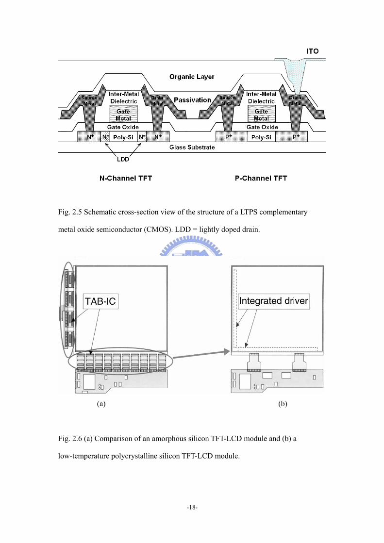
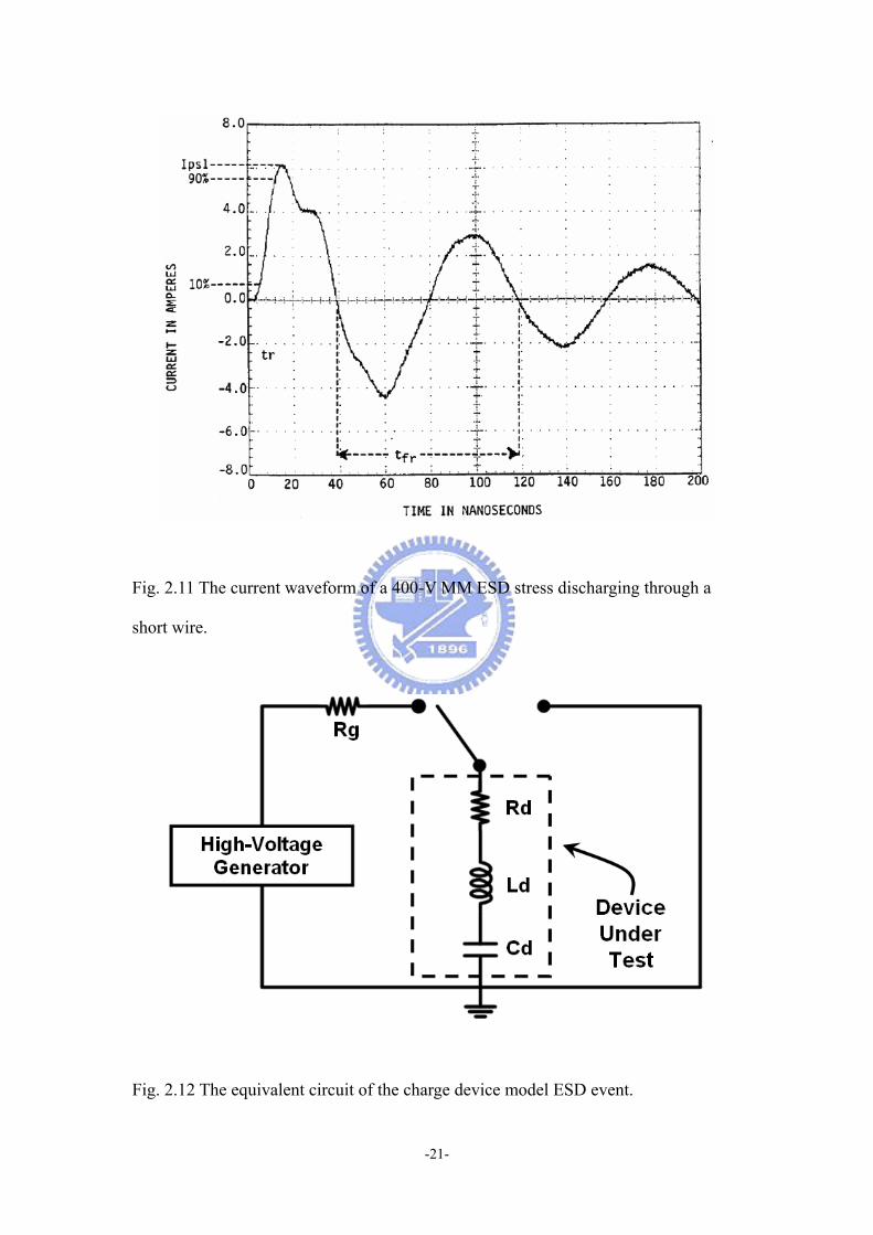
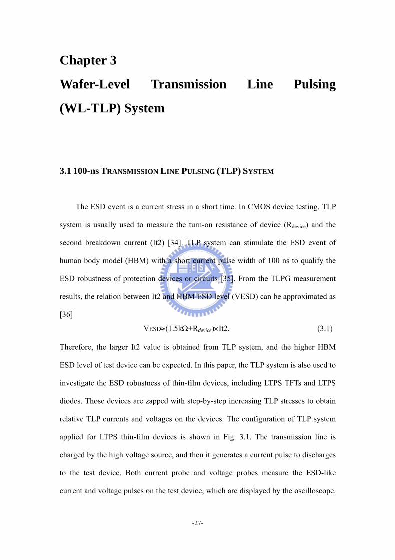
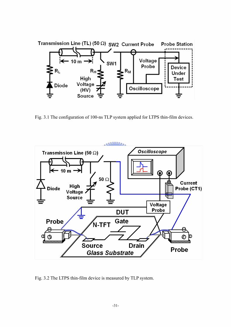
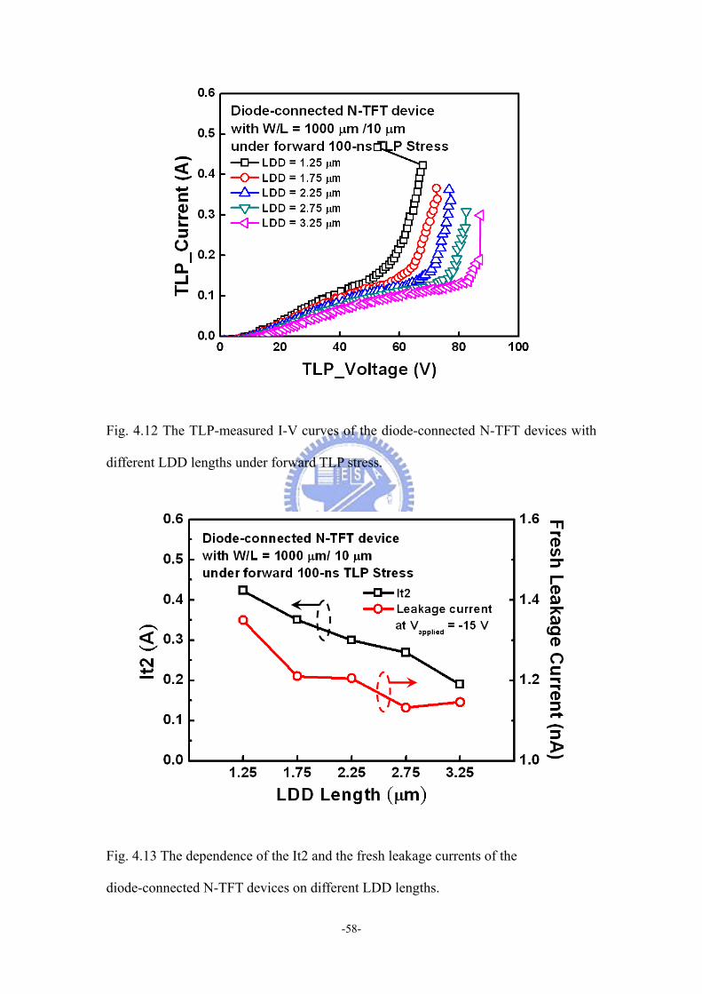
Related Documents