EECS 16B Designing Information Devices and Systems II Fall 2017 Note 1 1 Digital Information Processing Electrical circuits manipulate voltages ( V ) and currents (I ) in order to: 1. Process information (Arithmetics, Storage, Data Transfer, etc.) 2. Transduce energy to and from their environment (Sense, Actuate, Harvest energy, etc.) Because the universe appears analog (continuous in time and quantity) at our scale, we usually use analog circuits to interface with anything that interfaces with the outside world (i.e. sensors, actuators, antennas, etc.). We can also use analog circuits to perform a function such as divider circuits you saw in EE16A. However, processing information in the analog world is extremely challenging and analog information pro- cessing is shrinking! Why? You already experienced all the errors, variations and fluctuations exist in the real world in the EE16a labs. There are many sources for these errors in practice; for example, any two metal wires close enough together form a capacitor and their voltages affect each other (this effect is known as “Cross-talk”)! With billions of transistors on a centimeter-scale chip areas and wires with nanometer spac- ings, this effect happens very frequently and causes errors. This is one of multiple noise and error sources limiting the analog information processing performance and complexity. In this lecture, we are interested to see how we can build processors robust to noise and scalable to perform complex operations. In order to make the processing immune to the errors, we should leave some margin between the voltages we plan to use by segmenting the voltage domain. These margins are called Noise Margins. Let’s assume a circuit that contains a V DD volt independent voltage supply and a bunch of passive components. We know that all voltage nodes in the steady state are between 0 V and V DD since the components just form some sort of dividers! For analog processing any voltage from 0 V to V DD can show up at the input/output ports in the under the error-free conditions. Now let’s see how a “2-level” digital processing format (binary), where only 0 V and V DD are meant to show up at the ports under the error-free conditions. These kinda circuits are called digital, where voltages at the ports should accept only certain discontinuous values under error free conditions. Although, you may heard already about binary digital processing, the number of level can be any arbitrary number beside 2 as well. Next figure shows noise margins for 2- and 4-level digital processing. Notice binary digital processing provides the largest noise margins and makes the processing most immune to noise and error perturbations compared to the higher order processing formats. This is why most of digital systems are binary. EECS 16B, Fall 2017, Note 1 1

Welcome message from author
This document is posted to help you gain knowledge. Please leave a comment to let me know what you think about it! Share it to your friends and learn new things together.
Transcript

EECS 16B Designing Information Devices and Systems IIFall 2017 Note 1
1 Digital Information Processing
Electrical circuits manipulate voltages (V ) and currents (I) in order to:
1. Process information (Arithmetics, Storage, Data Transfer, etc.)
2. Transduce energy to and from their environment (Sense, Actuate, Harvest energy, etc.)
Because the universe appears analog (continuous in time and quantity) at our scale, we usually use analogcircuits to interface with anything that interfaces with the outside world (i.e. sensors, actuators, antennas,etc.). We can also use analog circuits to perform a function such as divider circuits you saw in EE16A.However, processing information in the analog world is extremely challenging and analog information pro-cessing is shrinking! Why? You already experienced all the errors, variations and fluctuations exist in thereal world in the EE16a labs. There are many sources for these errors in practice; for example, any two metalwires close enough together form a capacitor and their voltages affect each other (this effect is known as“Cross-talk”)! With billions of transistors on a centimeter-scale chip areas and wires with nanometer spac-ings, this effect happens very frequently and causes errors. This is one of multiple noise and error sourceslimiting the analog information processing performance and complexity. In this lecture, we are interested tosee how we can build processors robust to noise and scalable to perform complex operations.
In order to make the processing immune to the errors, we should leave some margin between the voltageswe plan to use by segmenting the voltage domain. These margins are called Noise Margins. Let’s assume acircuit that contains a V DD volt independent voltage supply and a bunch of passive components. We knowthat all voltage nodes in the steady state are between 0V and V DD since the components just form some sortof dividers! For analog processing any voltage from 0V to V DD can show up at the input/output ports inthe under the error-free conditions. Now let’s see how a “2-level” digital processing format (binary), whereonly 0V and V DD are meant to show up at the ports under the error-free conditions. These kinda circuits arecalled digital, where voltages at the ports should accept only certain discontinuous values under error freeconditions. Although, you may heard already about binary digital processing, the number of level can beany arbitrary number beside 2 as well. Next figure shows noise margins for 2- and 4-level digital processing.Notice binary digital processing provides the largest noise margins and makes the processing most immuneto noise and error perturbations compared to the higher order processing formats. This is why most ofdigital systems are binary.
EECS 16B, Fall 2017, Note 1 1
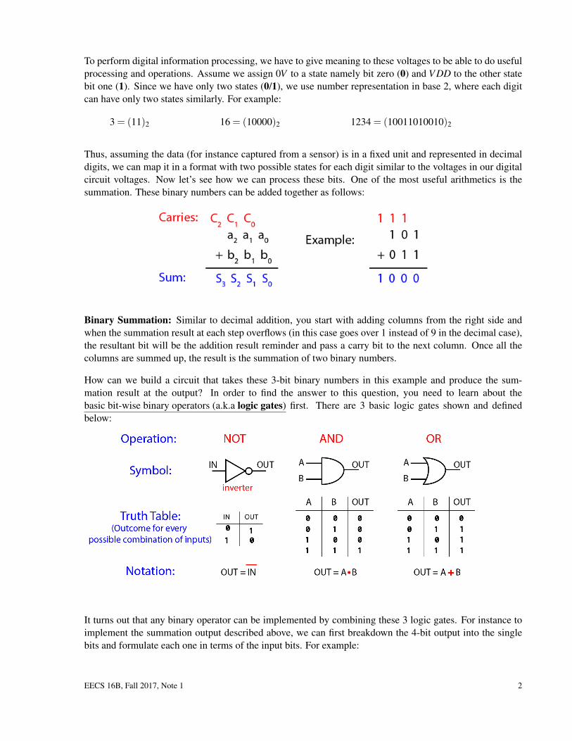
To perform digital information processing, we have to give meaning to these voltages to be able to do usefulprocessing and operations. Assume we assign 0V to a state namely bit zero (0) and V DD to the other statebit one (1). Since we have only two states (0/1), we use number representation in base 2, where each digitcan have only two states similarly. For example:
3 = (11)2 16 = (10000)2 1234 = (10011010010)2
Thus, assuming the data (for instance captured from a sensor) is in a fixed unit and represented in decimaldigits, we can map it in a format with two possible states for each digit similar to the voltages in our digitalcircuit voltages. Now let’s see how we can process these bits. One of the most useful arithmetics is thesummation. These binary numbers can be added together as follows:
Binary Summation: Similar to decimal addition, you start with adding columns from the right side andwhen the summation result at each step overflows (in this case goes over 1 instead of 9 in the decimal case),the resultant bit will be the addition result reminder and pass a carry bit to the next column. Once all thecolumns are summed up, the result is the summation of two binary numbers.
How can we build a circuit that takes these 3-bit binary numbers in this example and produce the sum-mation result at the output? In order to find the answer to this question, you need to learn about thebasic bit-wise binary operators (a.k.a logic gates) first. There are 3 basic logic gates shown and definedbelow:
It turns out that any binary operator can be implemented by combining these 3 logic gates. For instance toimplement the summation output described above, we can first breakdown the 4-bit output into the singlebits and formulate each one in terms of the input bits. For example:
EECS 16B, Fall 2017, Note 1 2

So we can derive S0 only from a0 and b0 and also generate C0 which will be used to calculate the next bit(S1). Similarly one can keep doing this and write a function for all the bits using only NOT, AND, and ORoperators:
S0 = (a0 •b0)+(a0 •b0)
C0 = a0 •b0
S1 = (a1 •b1 •C0)+(a1 •b1 •C0)+(a1 •b1 •C0)+(a1 •b1 •C0)
C1 = (a1 •b1)+(a1 •C0)+(C0 •b1)
.
.
In this course we are not focusing on how to implement arbitrary logic operations using the 3 basic logicgates (covered in 61C course). Instead, we will go over the details for building these basic 3 logic gates andsee how they are implemented in the physical world. Surprisingly, knowing these very basics can help usto understand what’s limiting the speed of state-of-the-art electronics (laptops, smart-phones, etc.) and whyplaying games with your cell phone cause them to ran out of battery quickly!
Starting from the first logic gate (NOT), an inverter, one idea to build such a block is to use an opamp:
Although this works fine, we need around 10-20 transistors (explained later) to build a single opamp whichis not affordable in terms of area and energy in practice! You will see how to build this gate using only twotransistors!
To do so, we first see how switches can be used to build these gates and later discuss how the switches arebuilt in the real world using devices called transistors.
Outline:
EECS 16B, Fall 2017, Note 1 3

1. Switch based Logic
2. Transistors
3. Resistors (R) and capacitors (C) in a transistor (Intro to capacitors)
4. RC circuits
(a) Setting up problems
(b) Writing differential equations (D.E.)
(c) Finding boundary conditions
(d) Solving D.E. !!
(e) Intuition
2 Switch based Logic
You already used switches in the 16A course for instance in the charge sharing capacitor circuits for touch-screen sensing. Although, we represented them as a 2-terminal device previously, there should be anotherterminal to electrically control the state of the switch as well! Let’s call this control terminal the Gate andwhenever the Gate voltage is high enough the switch is closed and while the Gate voltage is low enoughthe switch is open. In fact this control terminal existed in 16A labs but they were set by the Launch-Pador Arduino kits. Although, this definition sounds enough to know the state of switch by knowing the Gatevoltage, there’s still something missing! First of all, the voltage of a node should be referenced to anothernode and also we need to define a threshold voltage (Vth) to know what we meant by “high/low voltages”.Thus the complete switch symbol and definition can be explained as:
Now, let’s see how we can build an inverter by just using this switch and a resistor:
EECS 16B, Fall 2017, Note 1 4
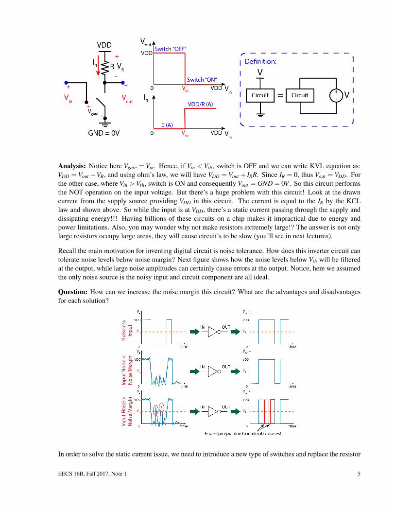
Analysis: Notice here Vgate = Vin. Hence, if Vin < Vth, switch is OFF and we can write KVL equation as:VDD = Vout +VR, and using ohm’s law, we will have VDD = Vout + IRR. Since IR = 0, thus Vout = VDD. Forthe other case, where Vin >Vth, switch is ON and consequently Vout = GND = 0V . So this circuit performsthe NOT operation on the input voltage. But there’s a huge problem with this circuit! Look at the drawncurrent from the supply source providing VDD in this circuit. The current is equal to the IR by the KCLlaw and shown above. So while the input is at VDD, there’s a static current passing through the supply anddissipating energy!!! Having billions of these circuits on a chip makes it impractical due to energy andpower limitations. Also, you may wonder why not make resistors extremely large!? The answer is not onlylarge resistors occupy large areas, they will cause circuit’s to be slow (you’ll see in next lectures).
Recall the main motivation for inventing digital circuit is noise tolerance. How does this inverter circuit cantolerate noise levels below noise margin? Next figure shows how the noise levels below Vth will be filteredat the output, while large noise amplitudes can certainly cause errors at the output. Notice, here we assumedthe only noise source is the noisy input and circuit component are all ideal.
Question: How can we increase the noise margin this circuit? What are the advantages and disadvantagesfor each solution?
In order to solve the static current issue, we need to introduce a new type of switches and replace the resistor
EECS 16B, Fall 2017, Note 1 5
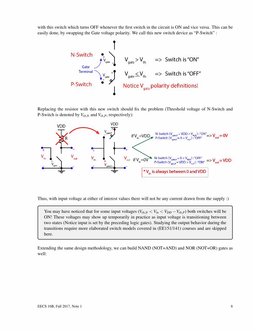
with this switch which turns OFF whenever the first switch in the circuit is ON and vice versa. This can beeasily done, by swapping the Gate voltage polarity. We call this new switch device as “P-Switch” :
Replacing the resistor with this new switch should fix the problem (Threshold voltage of N-Switch andP-Switch is denoted by Vth,N and Vth,P, respectively):
Thus, with input voltage at either of interest values there will not be any current drawn from the supply :)
You may have noticed that for some input voltages (Vth,N <Vin <VDD −Vth,P) both switches will beON! These voltages may show up temporarily in practice as input voltage is transitioning betweentwo states (Notice input is set by the preceding logic gates). Studying the output behavior during thetransitions require more elaborated switch models covered in (EE151/141) courses and are skippedhere.
Extending the same design methodology, we can build NAND (NOT+AND) and NOR (NOT+OR) gates aswell:
EECS 16B, Fall 2017, Note 1 6
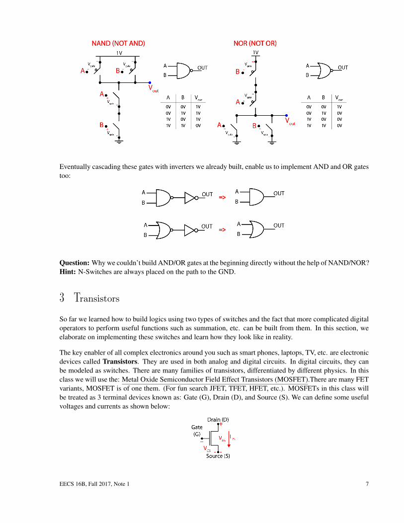
Eventually cascading these gates with inverters we already built, enable us to implement AND and OR gatestoo:
Question: Why we couldn’t build AND/OR gates at the beginning directly without the help of NAND/NOR?Hint: N-Switches are always placed on the path to the GND.
3 Transistors
So far we learned how to build logics using two types of switches and the fact that more complicated digitaloperators to perform useful functions such as summation, etc. can be built from them. In this section, weelaborate on implementing these switches and learn how they look like in reality.
The key enabler of all complex electronics around you such as smart phones, laptops, TV, etc. are electronicdevices called Transistors. They are used in both analog and digital circuits. In digital circuits, they canbe modeled as switches. There are many families of transistors, differentiated by different physics. In thisclass we will use the: Metal Oxide Semiconductor Field Effect Transistors (MOSFET).There are many FETvariants, MOSFET is of one them. (For fun search JFET, TFET, HFET, etc.). MOSFETs in this class willbe treated as 3 terminal devices known as: Gate (G), Drain (D), and Source (S). We can define some usefulvoltages and currents as shown below:
EECS 16B, Fall 2017, Note 1 7
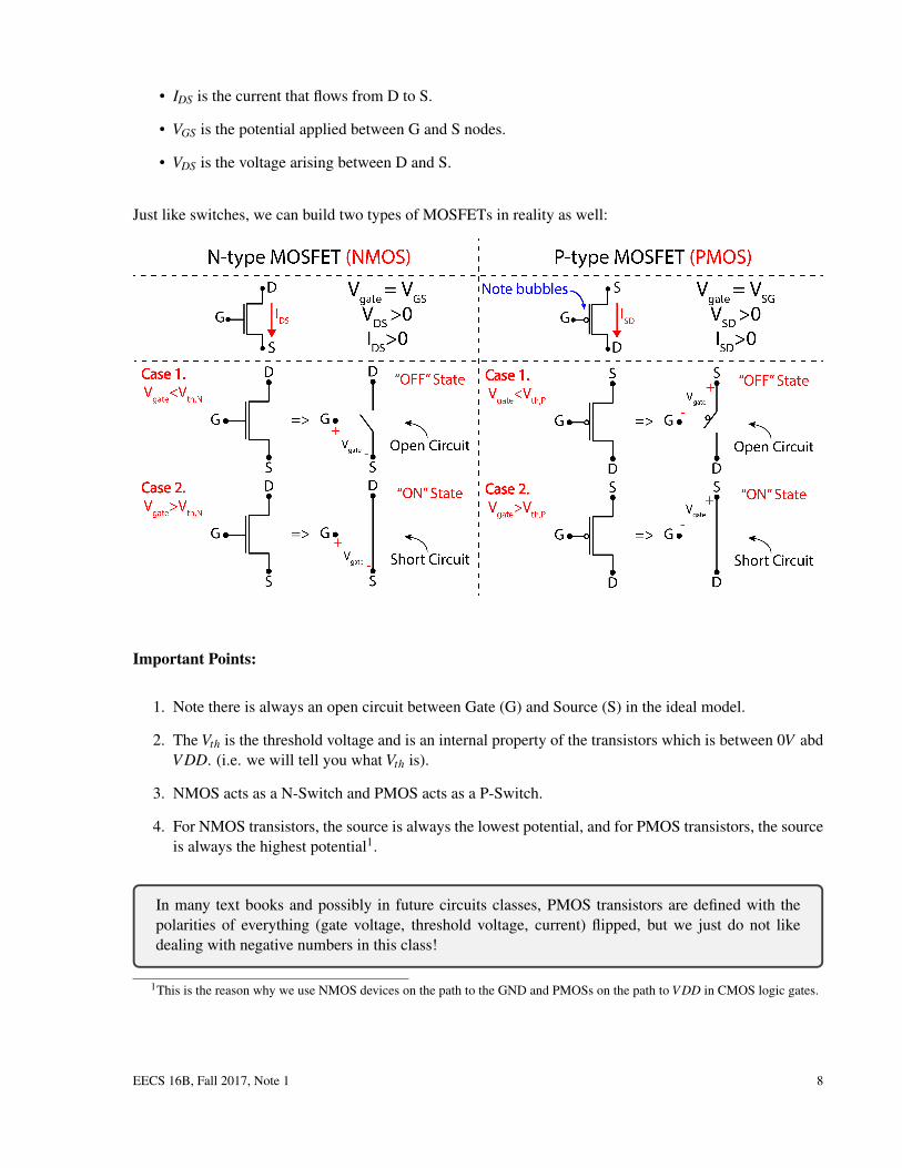
• IDS is the current that flows from D to S.
• VGS is the potential applied between G and S nodes.
• VDS is the voltage arising between D and S.
Just like switches, we can build two types of MOSFETs in reality as well:
Important Points:
1. Note there is always an open circuit between Gate (G) and Source (S) in the ideal model.
2. The Vth is the threshold voltage and is an internal property of the transistors which is between 0V abdV DD. (i.e. we will tell you what Vth is).
3. NMOS acts as a N-Switch and PMOS acts as a P-Switch.
4. For NMOS transistors, the source is always the lowest potential, and for PMOS transistors, the sourceis always the highest potential1.
In many text books and possibly in future circuits classes, PMOS transistors are defined with thepolarities of everything (gate voltage, threshold voltage, current) flipped, but we just do not likedealing with negative numbers in this class!
1This is the reason why we use NMOS devices on the path to the GND and PMOSs on the path to V DD in CMOS logic gates.
EECS 16B, Fall 2017, Note 1 8
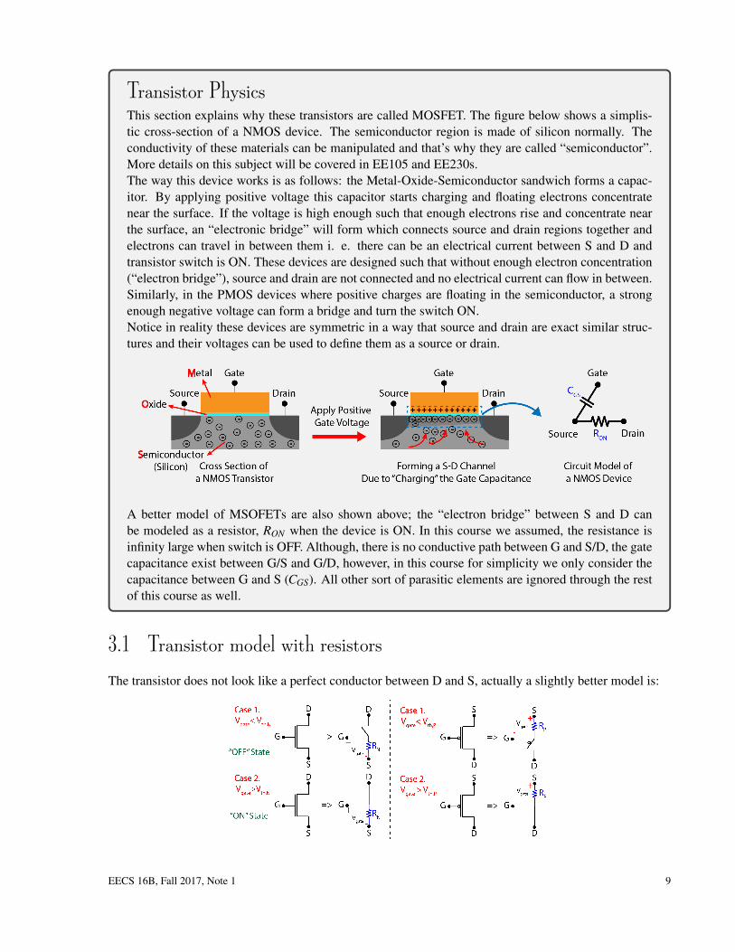
Transistor PhysicsThis section explains why these transistors are called MOSFET. The figure below shows a simplis-tic cross-section of a NMOS device. The semiconductor region is made of silicon normally. Theconductivity of these materials can be manipulated and that’s why they are called “semiconductor”.More details on this subject will be covered in EE105 and EE230s.The way this device works is as follows: the Metal-Oxide-Semiconductor sandwich forms a capac-itor. By applying positive voltage this capacitor starts charging and floating electrons concentratenear the surface. If the voltage is high enough such that enough electrons rise and concentrate nearthe surface, an “electronic bridge” will form which connects source and drain regions together andelectrons can travel in between them i. e. there can be an electrical current between S and D andtransistor switch is ON. These devices are designed such that without enough electron concentration(“electron bridge”), source and drain are not connected and no electrical current can flow in between.Similarly, in the PMOS devices where positive charges are floating in the semiconductor, a strongenough negative voltage can form a bridge and turn the switch ON.Notice in reality these devices are symmetric in a way that source and drain are exact similar struc-tures and their voltages can be used to define them as a source or drain.
A better model of MSOFETs are also shown above; the “electron bridge” between S and D canbe modeled as a resistor, RON when the device is ON. In this course we assumed, the resistance isinfinity large when switch is OFF. Although, there is no conductive path between G and S/D, the gatecapacitance exist between G/S and G/D, however, in this course for simplicity we only consider thecapacitance between G and S (CGS). All other sort of parasitic elements are ignored through the restof this course as well.
3.1 Transistor model with resistors
The transistor does not look like a perfect conductor between D and S, actually a slightly better model is:
EECS 16B, Fall 2017, Note 1 9

3.2 The CMOS Inverter
Now we introduce the Complimentary MOS (CMOS) Inverter. The PMOS and NMOS transistors act in acomplimentary way just like P-type and N-type switches and this is why they are called CMOS! The vestbulk of the digital circuit “chips” in your devices are built from CMOS logic gates.
This circuit is directly derived from the switch-based inverter schematic. Pay close attention to the G, D, andS labels. Note Vgate,N =Vin and Vgate,P =VDD−Vin and Vout =VDS,N . Before we analyze the CMOS inverter,let’s look at the first inverter we built using N-switch and resistance (called pseudo-NMOS inverter) shownbelow:
This figure revealed another issue of using only NMOS devices in addition to the static current in the ONstate. The problem is that using transistor models with resistors, the output voltage is not 0V and it is afunction of resistances and V DD. So for Vout to be low enough, R should be large again! However, in theCMOS inverter this issue does not exist:
EECS 16B, Fall 2017, Note 1 10

3.2.1 Simple CMOS logic gates
The trick to build other logic gates are similar to what we did using switches. Notice that the CMOS inverteris built from two blocks:
The job of the NMOS was to “pull down” the output to GND. Likewise, the job of the PMOS was to “pullup” the output to VDD. They never do this at the same time! This is the underlying concept behind the logicgates we built from P- and N-switches as well. The following is the CMOS NOR gate:
EECS 16B, Fall 2017, Note 1 11
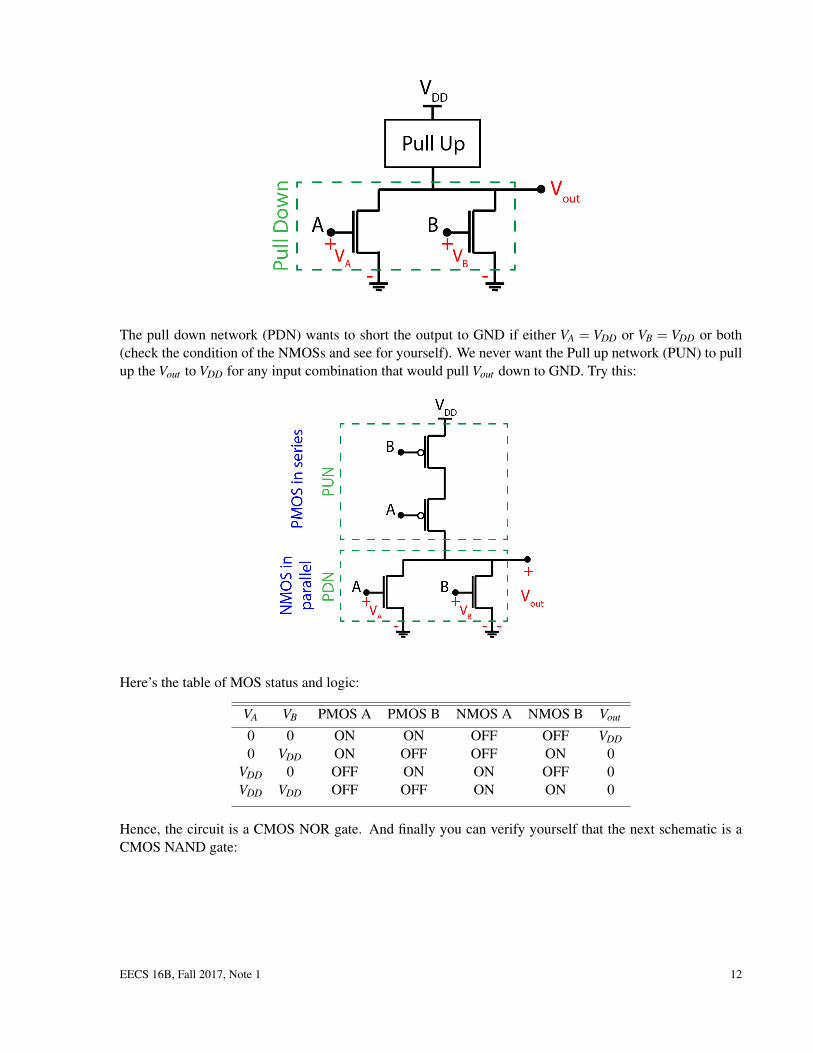
The pull down network (PDN) wants to short the output to GND if either VA = VDD or VB = VDD or both(check the condition of the NMOSs and see for yourself). We never want the Pull up network (PUN) to pullup the Vout to VDD for any input combination that would pull Vout down to GND. Try this:
Here’s the table of MOS status and logic:
VA VB PMOS A PMOS B NMOS A NMOS B Vout
0 0 ON ON OFF OFF VDD
0 VDD ON OFF OFF ON 0VDD 0 OFF ON ON OFF 0VDD VDD OFF OFF ON ON 0
Hence, the circuit is a CMOS NOR gate. And finally you can verify yourself that the next schematic is aCMOS NAND gate:
EECS 16B, Fall 2017, Note 1 12

Summary
• Digital processing can tolerate noise and errors to certain levels and this makes them favorable tobuild complex processors.
• Binary digital circuits have the largest noise immunity compared with higher order multi-level digitalsystems.
• Any binary operator can be implemented by 3 fundamental logic gates: NOT, OR, AND.
• We showed how to build these basic gates using P-switches and N-switches.
• It turns out NMOS and PMOS transistors act as N- and P- type switches, respectively.
• All the modern electronics around us are designed using CMOS gates and in the next lecture we willstudy the speed/power limitations of these circuits ...
EECS 16B, Fall 2017, Note 1 13
Related Documents