EECC551 - Shaaban EECC551 - Shaaban #1 lec # 9 Winter2000 1-16-20 Memory Hierarchy: The Memory Hierarchy: The motivation motivation • The gap between CPU performance and main memory has been widening with higher performance CPUs creating performance bottlenecks for memory access instructions. • The memory hierarchy is organized into several levels of memory with the smaller, more expensive, and faster memory levels closer to the CPU: registers, then primary Cache Level (L 1 ), then additional secondary cache levels (L 2 , L 3 …), then main memory, then mass storage (virtual memory). • Each level of the hierarchy is a subset of the level below: data found in a level is also found in the level below but at lower speed. • Each level maps addresses from a larger physical memory to a smaller level of physical memory. • This concept is greatly aided by the principal of locality both temporal and spatial which indicates that programs tend to reuse data and instructions that they have used recently or those stored in their vicinity leading to working set of a program.

EECC551 - Shaaban #1 lec # 9 Winter2000 1-16-2001 Memory Hierarchy: The motivation The gap between CPU performance and main memory has been widening with.
Dec 19, 2015
Welcome message from author
This document is posted to help you gain knowledge. Please leave a comment to let me know what you think about it! Share it to your friends and learn new things together.
Transcript
EECC551 - ShaabanEECC551 - Shaaban#1 lec # 9 Winter2000 1-16-2001
Memory Hierarchy: The motivationMemory Hierarchy: The motivation• The gap between CPU performance and main memory has been
widening with higher performance CPUs creating performance bottlenecks for memory access instructions.
• The memory hierarchy is organized into several levels of memory with the smaller, more expensive, and faster memory levels closer to the CPU: registers, then primary Cache Level (L1), then additional secondary cache levels (L2, L3…), then main memory, then mass storage (virtual memory).
• Each level of the hierarchy is a subset of the level below: data found in a level is also found in the level below but at lower speed.
• Each level maps addresses from a larger physical memory to a smaller level of physical memory.
• This concept is greatly aided by the principal of locality both temporal and spatial which indicates that programs tend to reuse data and instructions that they have used recently or those stored in their vicinity leading to working set of a program.
EECC551 - ShaabanEECC551 - Shaaban#2 lec # 9 Winter2000 1-16-2001
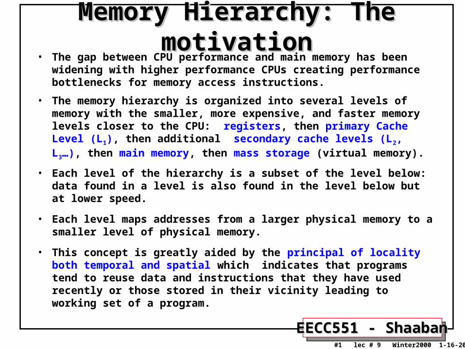
From Recent Technology TrendsFrom Recent Technology Trends Capacity Speed (latency)
Logic: 2x in 3 years 2x in 3 years
DRAM: 4x in 3 years 2x in 10 years
Disk: 4x in 3 years 2x in 10 years
DRAMYear Size Cycle Time1980 64 Kb 250 ns1983 256 Kb 220 ns1986 1 Mb 190 ns1989 4 Mb 165 ns1992 16 Mb 145 ns1995 64 Mb 120 ns
1000:1 2:1
EECC551 - ShaabanEECC551 - Shaaban#3 lec # 9 Winter2000 1-16-2001
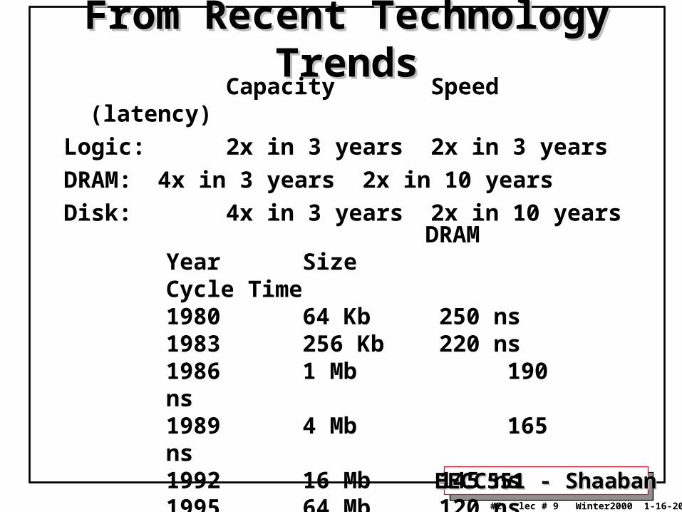
Memory Hierarchy: MotivationMemory Hierarchy: MotivationProcessor-Memory (DRAM) Performance GapProcessor-Memory (DRAM) Performance Gap
µProc60%/yr.
DRAM7%/yr.
1
10
100
1000198
0198
1 198
3198
4198
5 198
6198
7198
8198
9199
0199
1 199
2199
3199
4199
5199
6199
7199
8 199
9200
0
DRAM
CPU
198
2
Processor-MemoryPerformance Gap:(grows 50% / year)
Per
form
ance

EECC551 - ShaabanEECC551 - Shaaban#4 lec # 9 Winter2000 1-16-2001
Processor-DRAM Performance Gap Impact: Processor-DRAM Performance Gap Impact:
Example Example• To illustrate the performance impact, assume a pipelined RISC CPU with CPI = 1 using non-ideal
memory.
• Over an 10 year period, ignoring other factors, the cost of a full memory access in terms of number of wasted instructions:
CPU CPU Memory Minimum CPU cycles or Year speed cycle Access instructions wasted MHZ ns ns
1986: 8 125 190 190/125 = 1.51988: 33 30 175 175/30 = 5.81991: 75 13.3 155 155/13.3 = 11.651994: 200 5 130 130/5 = 261996: 300 3.33 100 110/3.33 = 33

EECC551 - ShaabanEECC551 - Shaaban#5 lec # 9 Winter2000 1-16-2001
Memory Hierarchy: MotivationMemory Hierarchy: Motivation
The Principle Of LocalityThe Principle Of Locality• Programs usually access a relatively small portion of their address
space (instructions/data) at any instant of time (program working set).
• Two Types of locality:
– Temporal Locality: If an item is referenced, it will tend to be referenced again soon.
– Spatial locality: If an item is referenced, items whose addresses are close will tend to be referenced soon.
• The presence of locality in program behavior, makes it possible to satisfy a large percentage of program access needs (both instructions and operands) using memory levels with much less capacity than program address space.
EECC551 - ShaabanEECC551 - Shaaban#6 lec # 9 Winter2000 1-16-2001
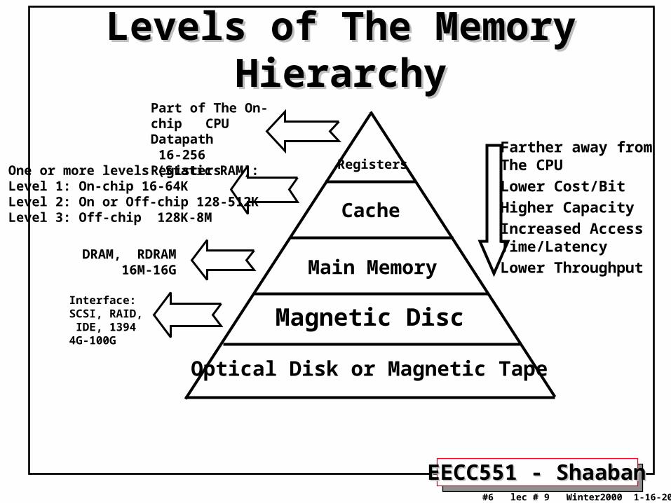
Levels of The Memory HierarchyLevels of The Memory HierarchyPart of The On-chip CPU Datapath 16-256 Registers
One or more levels (Static RAM):Level 1: On-chip 16-64K Level 2: On or Off-chip 128-512KLevel 3: Off-chip 128K-8M
Registers
Cache
Main Memory
Magnetic Disc
Optical Disk or Magnetic Tape
Farther away from The CPU
Lower Cost/Bit
Higher Capacity
Increased AccessTime/Latency
Lower ThroughputDRAM, RDRAM 16M-16G
Interface:SCSI, RAID, IDE, 13944G-100G

EECC551 - ShaabanEECC551 - Shaaban#7 lec # 9 Winter2000 1-16-2001
A Typical Memory HierarchyA Typical Memory Hierarchy ((With Two Levels of Cache)With Two Levels of Cache)
Control
Datapath
VirtualMemory,
SecondaryStorage(Disk)
Processor
Registers
MainMemory(DRAM)
SecondLevelCache
(SRAM)L2
1s 10,000,000s
(10s ms)
Speed (ns): 10s 100s
100s GsSize (bytes): Ks Ms
TertiaryStorage(Tape)
10,000,000,000s (10s sec)
Ts
On-ChipLevel OneCache L1
Larger CapacityFaster

EECC551 - ShaabanEECC551 - Shaaban#8 lec # 9 Winter2000 1-16-2001
Levels of The Memory HierarchyLevels of The Memory Hierarchy

EECC551 - ShaabanEECC551 - Shaaban#9 lec # 9 Winter2000 1-16-2001
SRAM Organization ExampleSRAM Organization Example 4 words X 3 bits each4 words X 3 bits each

EECC551 - ShaabanEECC551 - Shaaban#10 lec # 9 Winter2000 1-16-2001
Memory Hierarchy OperationMemory Hierarchy Operation• If an instruction or operand is required by the CPU, the levels of
the memory hierarchy are searched for the item starting with the level closest to the CPU (Level 1 cache):– If the item is found, it’s delivered to the CPU resulting in a cache hit
without searching lower levels.– If the item is missing from an upper level, resulting in a miss, the level
just below is searched. – For systems with several levels of cache, the search continues with
cache level 2, 3 etc.– If all levels of cache report a miss then main memory is accessed for
the item.• CPU cache memory: Managed by hardware.
– If the item is not found in main memory resulting in a page fault, then disk (virtual memory), is accessed for the item.• Memory disk: Managed by hardware and the operating
system.

EECC551 - ShaabanEECC551 - Shaaban#11 lec # 9 Winter2000 1-16-2001
Memory Hierarchy: TerminologyMemory Hierarchy: Terminology• A Block: The smallest unit of information transferred between two
levels.
• Hit: Item is found in some block in the upper level (example: Block X)
– Hit Rate: The fraction of memory access found in the upper level.
– Hit Time: Time to access the upper level which consists of
RAM access time + Time to determine hit/miss
• Miss: Item needs to be retrieved from a block in the lower level (Block Y)
– Miss Rate = 1 - (Hit Rate)
– Miss Penalty: Time to replace a block in the upper level +
Time to deliver the block the processor
• Hit Time << Miss Penalty
Lower LevelMemoryUpper Level
MemoryTo Processor
From ProcessorBlk X
Blk Y
EECC551 - ShaabanEECC551 - Shaaban#12 lec # 9 Winter2000 1-16-2001
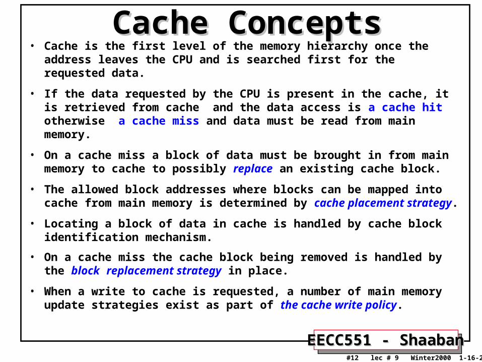
Cache ConceptsCache Concepts• Cache is the first level of the memory hierarchy once the address leaves
the CPU and is searched first for the requested data.
• If the data requested by the CPU is present in the cache, it is retrieved from cache and the data access is a cache hit otherwise a cache miss and data must be read from main memory.
• On a cache miss a block of data must be brought in from main memory to cache to possibly replace an existing cache block.
• The allowed block addresses where blocks can be mapped into cache from main memory is determined by cache placement strategy.
• Locating a block of data in cache is handled by cache block identification mechanism.
• On a cache miss the cache block being removed is handled by the block replacement strategy in place.
• When a write to cache is requested, a number of main memory update strategies exist as part of the cache write policy.

EECC551 - ShaabanEECC551 - Shaaban#13 lec # 9 Winter2000 1-16-2001
Cache Design & Operation IssuesCache Design & Operation Issues• Q1: Where can a block be placed cache?
(Block placement strategy & Cache organization)– Fully Associative, Set Associative, Direct Mapped.
• Q2: How is a block found if it is in cache? (Block identification)– Tag/Block.
• Q3: Which block should be replaced on a miss? (Block replacement)– Random, LRU.
• Q4: What happens on a write? (Cache write policy)– Write through, write back.

EECC551 - ShaabanEECC551 - Shaaban#14 lec # 9 Winter2000 1-16-2001
We will examineWe will examine:
• Cache Placement StrategiesCache Placement Strategies
– Cache OrganizationCache Organization
• Locating A Data Block in CacheLocating A Data Block in Cache
• Cache Replacement PolicyCache Replacement Policy
• What happens on cache Reads/WritesWhat happens on cache Reads/Writes
• Cache write strategiesCache write strategies
• Cache write miss policiesCache write miss policies
• Cache performanceCache performance

EECC551 - ShaabanEECC551 - Shaaban#15 lec # 9 Winter2000 1-16-2001
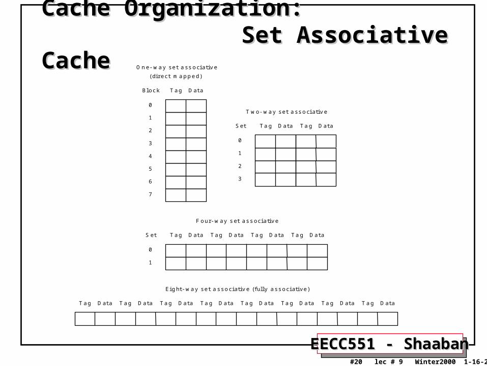
Cache Organization & Placement StrategiesCache Organization & Placement StrategiesPlacement strategies or mapping of a main memory data block onto
cache block frame addresses divide cache into three organizations:
1 Direct mapped cache: A block can be placed in one location only, given by:
(Block address) MOD (Number of blocks in cache)
2 Fully associative cache: A block can be placed anywhere in cache.
3 Set associative cache: A block can be placed in a restricted set of places, or cache block frames. A set is a group of block frames in the cache. A block is first mapped onto the set and then it can be placed anywhere within the set. The set in this case is chosen by:
(Block address) MOD (Number of sets in cache)
If there are n blocks in a set the cache placement is called n-way set-associative.

EECC551 - ShaabanEECC551 - Shaaban#16 lec # 9 Winter2000 1-16-2001
Cache Organization: Cache Organization: Direct Mapped CacheDirect Mapped Cache
0 0 0 0 1 0 0 1 0 1 0 1 0 0 1 0 1 1 0 1 1 0 0 0 1 1 0 1 0 1 1 1 0 0 1 1 1 1 0 1
00
0
C a c h e
M e m o ry
00
1
01
0
01
1
10
0
10
1
11
0
11
1
A block can be placed in one location only, given by: (Block address) MOD (Number of blocks in cache) In this case: (Block address) MOD (8)
32 memory blockscacheable
8 cache block frames

EECC551 - ShaabanEECC551 - Shaaban#17 lec # 9 Winter2000 1-16-2001
Direct-Mapped Cache Direct-Mapped Cache Example Example
A d d re s s (s h o w in g b it p o s i t io n s )
2 0 1 0
B y te
o ffs e t
V a l id T a g D a taIn d e x
0
1
2
1 0 2 1
1 0 2 2
1 0 2 3
T a g
In d e x
H i t D a ta
2 0 3 2
3 1 3 0 1 3 1 2 1 1 2 1 0
1024 BlocksEach block = one word
Can cache up to232 bytes of memory
Index fieldTag field

EECC551 - ShaabanEECC551 - Shaaban#18 lec # 9 Winter2000 1-16-2001
Direct Mapped Cache ExampleDirect Mapped Cache ExampleA d d re s s (s ho w in g b it p o s ition s)
1 6 1 2 B yte
o ffs e t
V T a g D a ta
H it D a ta
1 6 32
4 K
e n tr ie s
1 6 b its 12 8 b i ts
M u x
3 2 3 2 3 2
2
3 2
B lo c k o f fs e tIn d ex
T ag
3 1 16 1 5 4 3 2 1 04K blocksEach block = four words
Takes better advantage of spatial locality
Index fieldTag field
Word select

EECC551 - ShaabanEECC551 - Shaaban#19 lec # 9 Winter2000 1-16-2001
Alpha AXP 21064 Data Cache OrganizationAlpha AXP 21064 Data Cache Organization
Direct Mapped OrganizationDirect Mapped Organization
EECC551 - ShaabanEECC551 - Shaaban#20 lec # 9 Winter2000 1-16-2001
T a g D a ta T a g D a ta T a g D a ta T a g D a ta T a g D a ta T a g D a ta T a g D a ta T a g D a ta
E ig h t - w a y s e t a s s o c ia t iv e ( fu l ly a s s o c ia t iv e )
T a g D a t a T a g D a ta T a g D a ta T a g D a ta
F o u r - w a y s e t a s s o c ia t iv e
S e t
0
1
T a g D a t a
O n e - w a y s e t a s s o c ia t iv e
(d i re c t m a p p e d )
B lo c k
0
7
1
2
3
4
5
6
T a g D a ta
T w o - w a y s e t a s s o c ia t iv e
S e t
0
1
2
3
T a g D a ta
Cache Organization: Cache Organization: Set Associative CacheSet Associative Cache

EECC551 - ShaabanEECC551 - Shaaban#21 lec # 9 Winter2000 1-16-2001
Cache Organization ExampleCache Organization Example

EECC551 - ShaabanEECC551 - Shaaban#22 lec # 9 Winter2000 1-16-2001
Locating A Data Block in CacheLocating A Data Block in Cache• Each block frame in cache has an address tag.
• The tags of every cache block that might contain the required data are checked in parallel.
• A valid bit is added to the tag to indicate whether this entry contains a valid address.
• The address from the CPU to cache is divided into:
– A block address, further divided into:
• An index field to choose a block set in cache.
(no index field when fully associative).
• A tag field to search and match addresses in the selected set.
– A block offset to select the data from the block.
Block Address BlockOffsetTag Index

EECC551 - ShaabanEECC551 - Shaaban#23 lec # 9 Winter2000 1-16-2001
Address Field SizesAddress Field Sizes
Block Address BlockOffsetTag Index
Block offset size = log2(block size)
Index size = log2(Total number of blocks/associativity)
Tag size = address size - index size - offset sizeTag size = address size - index size - offset size
Physical Address Generated by CPU
EECC551 - ShaabanEECC551 - Shaaban#24 lec # 9 Winter2000 1-16-2001
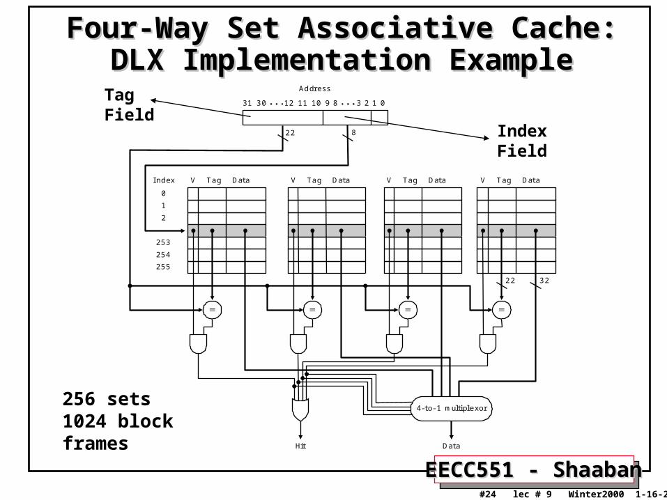
Four-Way Set Associative Cache:Four-Way Set Associative Cache:DLX Implementation ExampleDLX Implementation Example
Ad dress
2 2 8
V TagIndex
0
1
2
253
254
255
D ata V Tag D ata V Tag D ata V Tag D ata
3 22 2
4 - to - 1 m ultip lexo r
H it D a ta
123891011123 031 0
IndexField
TagField
256 sets1024 block frames

EECC551 - ShaabanEECC551 - Shaaban#25 lec # 9 Winter2000 1-16-2001
Alpha AXP 21064 Alpha AXP 21064 Data CacheData CacheOrganizationOrganization
Two-way Set-AssociativeTwo-way Set-AssociativeVersionVersion

EECC551 - ShaabanEECC551 - Shaaban#26 lec # 9 Winter2000 1-16-2001
Cache Organization/Addressing ExampleCache Organization/Addressing Example
• Given the following:
– A single-level cache with 128 cache block frames
• Each block frame contains four words (16 bytes)
– 16-bit memory addresses (64K bytes main memory or 4096 blocks)
• Show the cache organization/mapping and cache address fields for:
• Fully Associative cache
• Direct mapped cache
• 2-way set-associative cache

EECC551 - ShaabanEECC551 - Shaaban#27 lec # 9 Winter2000 1-16-2001
Cache Example: Fully Associative CaseCache Example: Fully Associative Case
Block offset = 4 bits
Block Address = 12 bits
Tag = 12 bits
All 128 tags mustbe checked in parallelby hardware to locate a data block
V
V
V
Valid bit
EECC551 - ShaabanEECC551 - Shaaban#28 lec # 9 Winter2000 1-16-2001
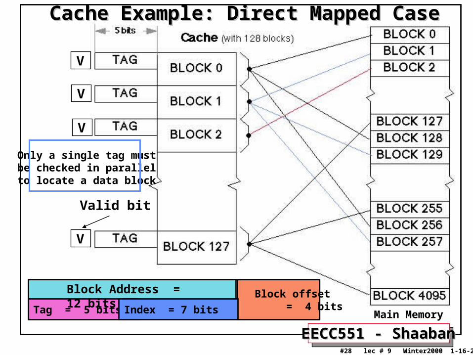
Cache Example: Direct Mapped CaseCache Example: Direct Mapped Case
Block offset = 4 bits
Block Address = 12 bits
Tag = 5 bits Index = 7 bits Main Memory
Only a single tag mustbe checked in parallelto locate a data block
V
Valid bit
V
V
V

EECC551 - ShaabanEECC551 - Shaaban#29 lec # 9 Winter2000 1-16-2001
Block offset = 4 bits
Block Address = 12 bits
Tag = 6 bits Index = 6 bits
Cache Example: 2-Way Set-AssociativeCache Example: 2-Way Set-Associative
Main Memory
Two tags in a set mustbe checked in parallelto locate a data block
Valid bits not shown

EECC551 - ShaabanEECC551 - Shaaban#30 lec # 9 Winter2000 1-16-2001
Cache Replacement PolicyCache Replacement Policy• When a cache miss occurs the cache controller may have to
select a block of cache data to be removed from a cache block frame and replaced with the requested data, such a block is selected by one of two methods:
– Random: • Any block is randomly selected for replacement providing
uniform allocation.
• Simple to build in hardware.
• The most widely used cache replacement strategy.
– Least-recently used (LRU): • Accesses to blocks are recorded and and the block
replaced is the one that was not used for the longest period of time.
• LRU is expensive to implement, as the number of blocks to be tracked increases, and is usually approximated.

EECC551 - ShaabanEECC551 - Shaaban#31 lec # 9 Winter2000 1-16-2001
Miss Rates for Caches with Different Size, Miss Rates for Caches with Different Size, Associativity & Replacement AlgorithmAssociativity & Replacement Algorithm
Sample DataSample Data
Associativity: 2-way 4-way 8-way
Size LRU Random LRU Random LRURandom
16 KB 5.18% 5.69% 4.67% 5.29% 4.39% 4.96%
64 KB 1.88% 2.01% 1.54% 1.66% 1.39% 1.53%
256 KB 1.15% 1.17% 1.13% 1.13% 1.12% 1.12%

EECC551 - ShaabanEECC551 - Shaaban#32 lec # 9 Winter2000 1-16-2001
Cache Read/Write OperationsCache Read/Write Operations• Statistical data suggest that reads (including instruction
fetches) dominate processor cache accesses (writes account for 25% of data cache traffic).
• In cache reads, a block is read at the same time while the tag is being compared with the block address. If the read is a hit the data is passed to the CPU, if a miss it ignores it.
• In cache writes, modifying the block cannot begin until the tag is checked to see if the address is a hit.
• Thus for cache writes, tag checking cannot take place in parallel, and only the specific data (between 1 and 8 bytes) requested by the CPU can be modified.
• Cache is classified according to the write and memory update strategy in place: write through, or write back.

EECC551 - ShaabanEECC551 - Shaaban#33 lec # 9 Winter2000 1-16-2001
Cache Write StrategiesCache Write Strategies1 Write Though: Data is written to both the cache block and to a
block of main memory.
– The lower level always has the most updated data; an important feature for I/O and multiprocessing.
– Easier to implement than write back.
– A write buffer is often used to reduce CPU write stall while data is written to memory.
2 Write back: Data is written or updated only to the cache block. The modified cache block is written to main memory when it’s being replaced from cache.
– Writes occur at the speed of cache– A status bit called a dirty bit, is used to indicate whether the block
was modified while in cache; if not the block is not written to main memory.
– Uses less memory bandwidth than write through.

EECC551 - ShaabanEECC551 - Shaaban#34 lec # 9 Winter2000 1-16-2001
Cache Write Miss PolicyCache Write Miss Policy• Since data is usually not needed immediately on a write miss
two options exist on a cache write miss:
Write Allocate:
The cache block is loaded on a write miss followed by write hit actions.
No-Write Allocate:
The block is modified in the lower level (lower cache level, or main
memory) and not loaded into cache.
While any of the above two write miss policies can be used with either write back or write through:
• Write back caches use write allocate to capture subsequent writes to the block in cache.
• Write through caches usually use no-write allocate since subsequent writes still have to go to memory.

EECC551 - ShaabanEECC551 - Shaaban#35 lec # 9 Winter2000 1-16-2001
Cache PerformanceCache PerformanceFor a CPU with a single level (L1) of cache and no stalls for
cache hits:
CPU time = (CPU execution clock cycles +
Memory stall clock cycles) x clock cycle time
Memory stall clock cycles = (Reads x Read miss rate x Read miss penalty) + (Writes x Write miss rate x Write miss penalty)
If write and read miss penalties are the same:
Memory stall clock cycles = Memory accesses x Miss rate x Miss penalty
With ideal memory

EECC551 - ShaabanEECC551 - Shaaban#36 lec # 9 Winter2000 1-16-2001
Cache PerformanceCache Performance CPUtime = Instruction count x CPI x Clock cycle time
CPIexecution = CPI with ideal memory
CPI = CPIexecution + Mem Stall cycles per instruction
CPUtime = Instruction Count x (CPIexecution +
Mem Stall cycles per instruction) x Clock cycle time
Mem Stall cycles per instruction = Mem accesses per instruction x Miss rate x Miss penalty
CPUtime = IC x (CPIexecution + Mem accesses per instruction x
Miss rate x Miss penalty) x Clock cycle time
Misses per instruction = Memory accesses per instruction x Miss rate
CPUtime = IC x (CPIexecution + Misses per instruction x Miss penalty) x
Clock cycle time
EECC551 - ShaabanEECC551 - Shaaban#37 lec # 9 Winter2000 1-16-2001
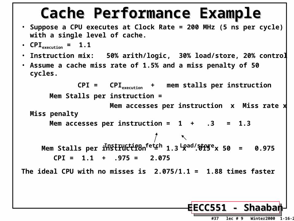
Cache Performance ExampleCache Performance Example• Suppose a CPU executes at Clock Rate = 200 MHz (5 ns per cycle) with a
single level of cache.
• CPIexecution = 1.1
• Instruction mix: 50% arith/logic, 30% load/store, 20% control• Assume a cache miss rate of 1.5% and a miss penalty of 50 cycles.
CPI = CPIexecution + mem stalls per instruction
Mem Stalls per instruction =
Mem accesses per instruction x Miss rate x Miss penalty
Mem accesses per instruction = 1 + .3 = 1.3
Mem Stalls per instruction = 1.3 x .015 x 50 = 0.975
CPI = 1.1 + .975 = 2.075
The ideal CPU with no misses is 2.075/1.1 = 1.88 times faster
Instruction fetch Load/store

EECC551 - ShaabanEECC551 - Shaaban#38 lec # 9 Winter2000 1-16-2001
Typical Cache Performance DataTypical Cache Performance Data Using SPEC92Using SPEC92

EECC551 - ShaabanEECC551 - Shaaban#39 lec # 9 Winter2000 1-16-2001
Cache Performance ExampleCache Performance ExampleTo compare the performance of either using a 16-KB instruction cache and
a 16-KB data cache as opposed to using a unified 32-KB cache, we assume a hit to
take one clock cycle and a miss to take 50 clock cycles, and a load or store to take
one extra clock cycle on a unified cache, and that 75% of memory accesses are
instruction references. Using the miss rates for SPEC92 we get:
Overall miss rate for a split cache = (75% x 0.64%) + (25% x 6.74%) = 2.1%
From SPEC92 data a unified cache would have a miss rate of 1.99%
Average memory access time =
= % instructions ( Read hit time + Read miss rate x Miss penalty)
+ % data x ( Write hit time + Write miss rate x Miss penalty)
For split cache:
Average memory access timesplit = 75% x ( 1 + 0.64 x 50) + (1+6.47%x50) = 2.05
For unified cache:
Average memory access timeunified = 75% x ( 1 + 1.99%) x 50) +
25% x ( 1 + 1+ 1.99% x 50)
= 2.24 cycles
EECC551 - ShaabanEECC551 - Shaaban#40 lec # 9 Winter2000 1-16-2001
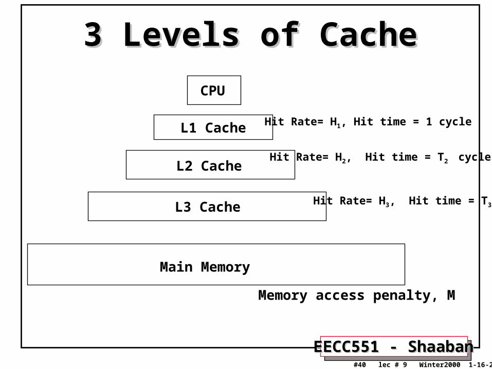
3 Levels of Cache3 Levels of Cache
CPU
L1 Cache
L2 Cache
L3 Cache
Main Memory
Hit Rate= H1, Hit time = 1 cycle
Hit Rate= H2, Hit time = T2 cycles
Hit Rate= H3, Hit time = T3
Memory access penalty, M

EECC551 - ShaabanEECC551 - Shaaban#41 lec # 9 Winter2000 1-16-2001
CPUtime = IC x (CPIexecution + Mem Stall cycles per instruction) x CMem Stall cycles per instruction = Mem accesses per instruction x Stall cycles per access
• For a system with 3 levels of cache, assuming no penalty when found in L1 cache:
Stall cycles per memory access =
[miss rate L1] x [ Hit rate L2 x Hit time L2
+ Miss rate L2 x (Hit rate L3 x Hit time L3
+ Miss rate L3 x Memory access penalty) ] =
[1 - H1] x [ H2 x T2
+ ( 1-H2 ) x (H3 x (T2 + T3)
+ (1 - H3) x M) ]
3-Level Cache Performance 3-Level Cache Performance

EECC551 - ShaabanEECC551 - Shaaban#42 lec # 9 Winter2000 1-16-2001
Three Level Cache Performance ExampleThree Level Cache Performance Example• CPU with CPIexecution = 1.1 running at clock rate = 500 MHZ
• 1.3 memory accesses per instruction.• L1 cache operates at 500 MHZ with a miss rate of 5%
• L2 cache operates at 250 MHZ with miss rate 3%, (T2 = 2 cycles)
• L3 cache operates at 100 MHZ with miss rate 1.5%, (T3 = 5 cycles)
• Memory access penalty, M= 100 cycles. Find CPI.
• With single L1, CPI = 1.1 + 1.3 x .05 x 100 = 7.6
CPI = CPIexecution + Mem Stall cycles per instruction
Mem Stall cycles per instruction = Mem accesses per instruction x Stall cycles per access Stall cycles per memory access = [1 - H1] x [ H2 x T2 + ( 1-H2 ) x (H3 x (T2 + T3)
+ (1 - H3) x M) ]
= [.05] x [ .97 x 2 + (.03) x ( .985 x (2+5)
+ .015 x 100)]
= .05 x [ 1.94 + .03 x ( 6.895 + 1.5) ]
= .05 x [ 1.94 + .274] = .11
• CPI = 1.1 + 1.3 x .11 = 1.24
Related Documents