EE552 Project Final Documentation 3D Graphics Processing Unit Eric Tan [email protected] Imran Waheed [email protected] Jeff Mrochuk [email protected] Benj Carson [email protected]

Welcome message from author
This document is posted to help you gain knowledge. Please leave a comment to let me know what you think about it! Share it to your friends and learn new things together.
Transcript
EE552 Project Final Documentation
3D Graphics Processing Unit
Eric Tan
Imran Waheed [email protected]
Jeff Mrochuk
Benj Carson [email protected]

2
DECLARATION OF ORIGINAL CONTENT The design elements of this project and report are entirely the original work of the authors and have not been submitted for credit in any other course except as follows:
• The VGA Output module was based on razzle.vhd by Jim Hamblen, Georgia Tech School The VGA Output module was based on razzle.vhd by Jim Hamblen, Georgia Tech School The VGA Output module was based on razzle.vhd by Jim Hamblen, Georgia Tech School The VGA Output module was based on razzle.vhd by Jim Hamblen, Georgia Tech School of ECE.of ECE.of ECE.of ECE.
• ZZZZ----BuffeBuffeBuffeBuffer pseudocode from Scott Owen: r pseudocode from Scott Owen: r pseudocode from Scott Owen: r pseudocode from Scott Owen: http://www.siggraph.org/education/materials/HyperGraph/scanline/visibility/zbuffer.htm.http://www.siggraph.org/education/materials/HyperGraph/scanline/visibility/zbuffer.htm.http://www.siggraph.org/education/materials/HyperGraph/scanline/visibility/zbuffer.htm.http://www.siggraph.org/education/materials/HyperGraph/scanline/visibility/zbuffer.htm.
• altclocklock & lpm_fifo_dc altclocklock & lpm_fifo_dc altclocklock & lpm_fifo_dc altclocklock & lpm_fifo_dc megafunctions are courtesy Altera (included in Quartusmegafunctions are courtesy Altera (included in Quartusmegafunctions are courtesy Altera (included in Quartusmegafunctions are courtesy Altera (included in Quartus II).II).II).II).
• The Incredible Hulk is a trademark of Marvel EnterpThe Incredible Hulk is a trademark of Marvel EnterpThe Incredible Hulk is a trademark of Marvel EnterpThe Incredible Hulk is a trademark of Marvel Enterprises, Inc. and Marvel Characters,rises, Inc. and Marvel Characters,rises, Inc. and Marvel Characters,rises, Inc. and Marvel Characters, Inc.Inc.Inc.Inc.
• mux3x48 is an Altera templatemux3x48 is an Altera templatemux3x48 is an Altera templatemux3x48 is an Altera template
• All Memory timings came from JEDEC PC133 Design Spec 4All Memory timings came from JEDEC PC133 Design Spec 4All Memory timings came from JEDEC PC133 Design Spec 4All Memory timings came from JEDEC PC133 Design Spec 4----20202020----02020202----R11b.R11b.R11b.R11b. Eric Tan Imran Waheed Jeff Mrochuk Benj Carson
3
ABSTRACT The ‘HULKHULKHULKHULK’ 3D Graphics Processing Unit (GPU) is a VHDL implementation of common 3D graphics rendering and transformation processor. It is capable of displaying a mesh composed of triangles on a VGA display. The design can be broken down into a VGA output module, two frame buffers, a z-buffer (for depth information), a transformation engine, a triangle rasterizer, an SDRAM controller and storage for triangle information. This document outlines the design and simulation of these units.

4
TABLE OF CONTENTS Declaration of Original Content 2 Abstract 3 Table of Contents 4 The State of the Hulk: 5 Description of Operation 6 Procedural Description 7
VGA Out 8 Frame Buffers 9 Triangle Rasterizer 9 Z-Buffer 11 Vertex Buffers 11 Matrix ALU & Transform Engine 11 Memory Interface 12
Input/Output Pins 14 Logic Block Requirements 15 Design Verification 15
Speed Information 16 Experiments and Characterization 16
Data Mask Experiments 16 SDRAM Speed Experiments 17
Slope Calculation Speed/Area Tradeoffs 17 Triage 17 References 18 Appendix A 19
Design Hierarchy 19 Appendix B 21
VHDL Code & Index 21 Appendix C 23
Simulation Waveforms 23 Appendix D 29
Schematics 29 Appendix E 31
Datasheets 31

5
THE STATE OF THE HULK:
What Works and What Doesn’tWhat Works and What Doesn’tWhat Works and What Doesn’tWhat Works and What Doesn’t Features CompleteFeatures CompleteFeatures CompleteFeatures Complete • SDRAM Controller • VGA Out • VGA out reading from dual SDRAM frame buffers • Z-Buffer for depth information • Dedicated Divide/Slope (For Raster and Transform) • Triangle Storage/Sorter with LPM RAM • Arbitrary Location Write • Write Masking (for individual pixel writing) • Trig look up table • Rasterization Unit Features Under DevelopmentFeatures Under DevelopmentFeatures Under DevelopmentFeatures Under Development
• Integration of transformation engine and Z-Buffer
The features under development are still targeted for completion within the next few days, and barring any unforeseen problems there will be no feature cuts. A more in-depth description of each unit is available in the Procedural Description Section.

6
DESCRIPTION OF OPERATION The GPU processes and displays a mesh of triangles colored and shaded triangles. One or more default triangle meshes will be loaded during device initialization. The vertices will be translated and rotated as specified by user input. The transformations require matrix math operations and trig functions, so a matrix ALU is required, as well as a trig lookup table. Once the triangles have been transformed, they are to be processed according to their depth (via a z-buffer) and rasterized. Two frame buffers will be used so that read and write operations are separated. These steps are shown in figure 1, below:
Figure Figure Figure Figure 1111: GPU Flowchart: GPU Flowchart: GPU Flowchart: GPU Flowchart
The Nios board system clock is 33 MHz. The SDRAM DIMM used in this design operates at speeds up to 100 MHz. As of the time of writing, all internal modules operate at least at 50 MHz. Since the VGA output module is not required to run at 50 MHz (see below), bottlenecks created by VGA module memory accesses can be reduced if it runs below the speed. Other modules are able to access memory during intervals of blank pixels at the end of every line and frame. Internal clock increasing is achieved using the built-in altclocklock megafunction. This instantiates a PLL, which multiplies the internal frequency of the clock.
7
PROCEDURAL DESCRIPTION
On a reset, the main control unit writes a simple pattern to the two 640x480 frame buffer and loads some initial stored vertices. The vertices are sent through the slope unit, which both calculates the slopes required and projects the (x,y,z) coordinates to the 2 dimensional (x,y) plane for display. After the clear, the control unit goes into a read cycle, which fills up a FIFO with one full line (640) of pixels. Then the FIFO is emptied as the vga_out unit requests them. It repeats this for 480 lines, and starts again. VGA blanking intervals provide dead time after every line and after every frame. Memory control is given to the write FIFO during these intervals, so it can write new data into the second framebuffer. These accesses are either drawing triangles to the frame buffer or reading/writing to the Z-buffer. The arbitrary write unit can write information to any address during the dead times. After a triangle is drawn the Z value of every point is dumped into a Z-buffer, so that when a second triangle is drawn, the rasterizer can calculate whether it is in front of or behind previous triangles. Recently completed was Pixel Masking. The SDRAM is being writen to in 4 bursts of 64-bits, which works out to 32 pixels at a time. To avoid a costly and memory-intensive read-modify-write cycle, the rasterizer must mask which pixels are written, or it would be overwriting data which should be displayed. The DQM function of SDRAM is perfect for this operation as it can mask one byte (a pixel) individually. Basically, the GPU performs all write operations in all dead time after reads, and swaps the two frame buffers after a full page is written. The Z buffer controls what gets written above or below, and masking allows the rasterizer to overwrite without reading from the current framebuffer. A more specific description of each unit is available in the following pages.

8
VGA Out The VGA output module is responsible for displaying the pixels stored in the frame buffer on the screen as well as generating blanking signals. Since the Nios board used in this project has a system clock frequency of 33 MHz, non-standard blanking timings are required. For simplicity, the pixel clock frequency is identical to the system clock frequency. The standard 640x480 VGA resolution is also used. A Matrox G400 video card was used to test accurate front porch, sync and back porch timings, the following settings were determined to work with a Samsung 900NF, a Panasonic E771 (the models in CEB 342) and a Daytek 17” monitors:
Horizontal Timing: Horizontal refresh 40.8 kHz Active 640 pixels 19.17µs Front Porch 43 pixels 1.29 µs Sync 46 pixels 1.38 µs Back Porch 87 pixels 2.61 µs Entire line 816 pixels 24.48 µs
Vertical Timing: Vertical refresh 76 Hz Active 480 lines 11.75 ms Front Porch 9 lines 0.223 ms Sync 3 lines 73.44 µs Back Porch 30 lines 0.734 ms Entire frame 522 lines 12.8 ms
According to their datasheets and specifications, the maximum vertical refresh for all these monitors is well over 90 Hz. The Viewsonic has a maximum vertical refresh at 640x480 of 120 Hz. The Samsung has a maximum vertical refresh of 160 Hz. These timings, although non-standard, are within the tolerances of the monitors. The VGA module has been successfully implemented and tested in hardware. Memory interfacing is pending the completion of the SDRAM controller, but the VGA module is able to correctly sync a monitor and display hard-coded pixels on the screen. Full code and waveforms are included in the appendix. 8 bits-per-pixel colour is obtained using a simple D to A converter. The schematic for the converter is included in the appendix. An array of resistors are used with the following values: For 3-bit colours (i.e. red and green):
Ω=
Ω==
4.4717.0100•3.3•
RV
VV
RVRON
DDD

9
Each bit has twice the significance of the preceding bit, so its output voltage should be twice as high. Since the maximum voltage for a VGA colour signal is 0.7V, the LSB should produce 0.1V, the middle bit 0.2V and the MSB 0.4V for a total of 0.7V:
Ω=Ω
=
Ω=Ω
=
Ω=Ω
=
kV
VR
kV
VR
VVR
3.31.0100•3.3
65.12.0100•3.3
8254.0100•3.3
0
1
2
For 2-bit colour (i.e. blue) the LSB should produce 0.2333V and the MSB 0.4666V for a total of 0.7V:
Ω=Ω
=
Ω=Ω
=
kV
VR
VVR
41.1233.0
100•3.3
7074667.0
100•3.3
0
1
Frame Buffers The frame buffers are simply areas of memory that store red, green and blue values for all the pixels on the screen. Since the HULKHULKHULKHULK uses 8 bits per pixel, red and green uses 3 bits and blue uses two. Two frame buffers are stored in SDRAM. The “read” frame buffer is accessed by the VGA output module and the “write” frame buffer is modified by the rasterizer. When rasterization is complete, the buffers are swapped (i.e. the VGA module accesses the newly completed frame and the rasterizer overwrites the previous one). The rasterizer control module arbitrates access to the buffers. Triangle Rasterizer The triangle rasterizer reads triangle information and writes the appropriate pixel values into the frame buffer. It takes the z-values of the vertices and corrects the x and y values for perspective using the perspective transformation (see calculations below). It also compares the RGB and xyz values generated by the triangle rasterizer and the z value stored in the z-buffer, and determines if the generated pixel is nearer to the viewer than the one in the z-buffer. Pixels with higher z values will be kept and displayed. The output of the rasterizer needs to be compatible with the memory controller. Since the memory controller writes 32 Bytes at a time, the rasterizer output is padded to 32 bits, and realigned to proper memory addresses. Since this will overwrite the existing contents of the frame buffer, values not within the triangle need to be byte masked, so current memory is not overwritten.

10
If λ is the focal length of the “camera” used to image the scene, then the x and y values on the screen of a point in space are given from:
world
worldimage z
xx−λ
=
world
worldimage z
yy−λ
=
Triangle Rasterizer AlgorithmTriangle Rasterizer AlgorithmTriangle Rasterizer AlgorithmTriangle Rasterizer Algorithm:
Take three vertices (p0, p1, p2) and use those to calculate three edge equations (edge01, edge12, edge20). The three edge equations will have the form Ax + By + C. The three coefficients are determined by:
( ) ( )[ ]10012
101
10
yyBxxACxxByyA
++−−=
−=
−=
The three coefficients have to be inverted so the edge walking technique can be utilized. The display is scanned from top-left to bottom-right going from left to right. The x and y coordinates of the pixel will be substituted into the three edge equations, and if all the three edge equation yield positive values the pixel is contained within the triangle. If the equation produces a zero it means that the pixel lies on the edge equation.
11
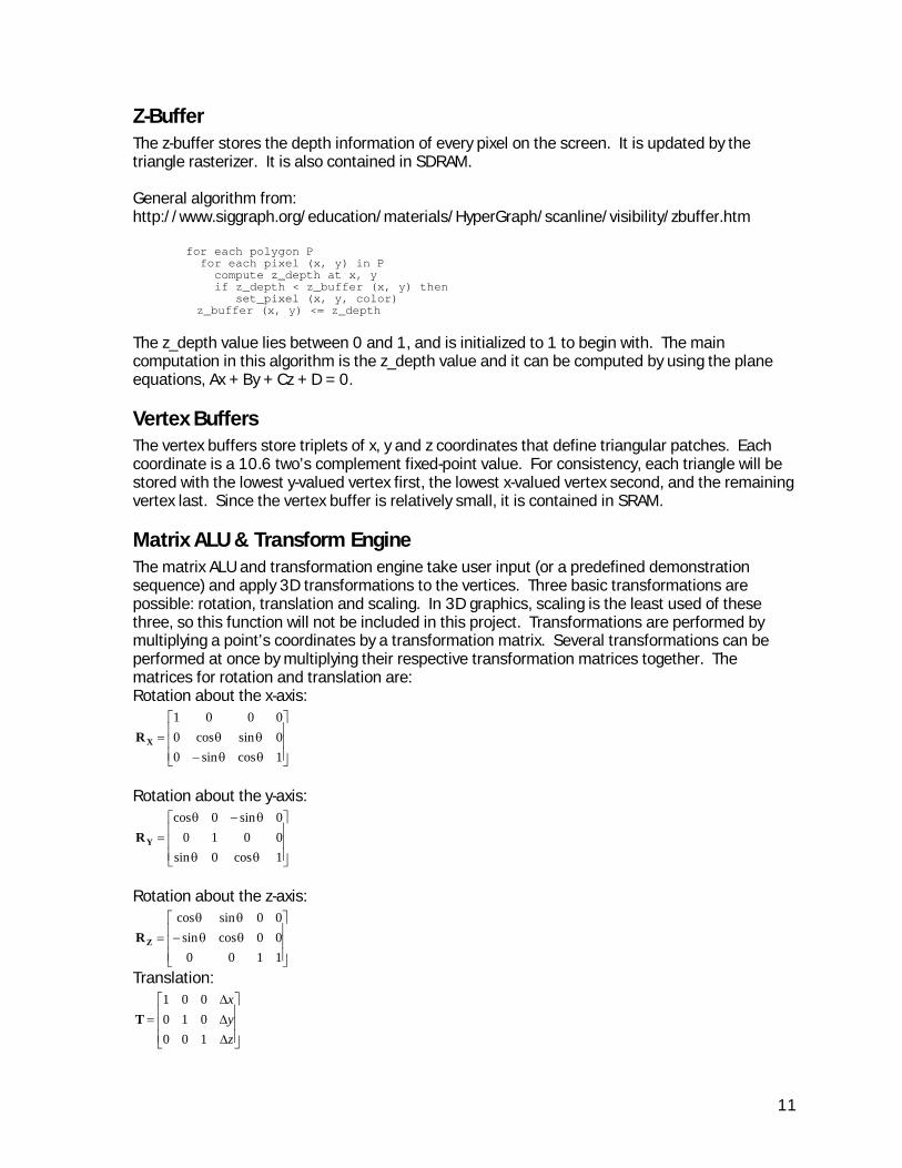
Z-Buffer The z-buffer stores the depth information of every pixel on the screen. It is updated by the triangle rasterizer. It is also contained in SDRAM. General algorithm from: http://www.siggraph.org/education/materials/HyperGraph/scanline/visibility/zbuffer.htm for each polygon P for each pixel (x, y) in P compute z_depth at x, y if z_depth < z_buffer (x, y) then set_pixel (x, y, color) z_buffer (x, y) <= z_depth The z_depth value lies between 0 and 1, and is initialized to 1 to begin with. The main computation in this algorithm is the z_depth value and it can be computed by using the plane equations, Ax + By + Cz + D = 0. Vertex Buffers The vertex buffers store triplets of x, y and z coordinates that define triangular patches. Each coordinate is a 10.6 two’s complement fixed-point value. For consistency, each triangle will be stored with the lowest y-valued vertex first, the lowest x-valued vertex second, and the remaining vertex last. Since the vertex buffer is relatively small, it is contained in SRAM. Matrix ALU & Transform Engine The matrix ALU and transformation engine take user input (or a predefined demonstration sequence) and apply 3D transformations to the vertices. Three basic transformations are possible: rotation, translation and scaling. In 3D graphics, scaling is the least used of these three, so this function will not be included in this project. Transformations are performed by multiplying a point’s coordinates by a transformation matrix. Several transformations can be performed at once by multiplying their respective transformation matrices together. The matrices for rotation and translation are: Rotation about the x-axis:
θθ−θθ=
1cossin00sincos00001
XR
Rotation about the y-axis:
θθ
θ−θ=
1cos0sin00100sin0cos
YR
Rotation about the z-axis:
θθ−θθ
=110000cossin00sincos
ZR
Translation:
∆∆∆
=zyx
100010001
T

12
To apply these transformations, the original point must be augmented to form a 4x1 column vector. For example to rotate a point about the z-axis by an amount θ:
θθ−θθ
=
1110000cossin00sincos
'''
zyx
zyx
The following equations were used for these transformations:
+×−××+×=
=
1sincossincos
θθθθ
yzzy
x
zyx
XR
+×−×
×−×=
=
1sincos
sincos
θθ
θθ
xzy
zx
zyx
YR
+×−××+×
=
=
1sincossincos
zxyyx
zyx
θθθθ
ZR
A trigonometric look up table was created to obtain the sine and cosine values required for these transformations. The unit accepts a triangle of three vertices. Each vertex is 48 bits and contains an x, y and z value in 10.6 two’s complement fixed-point notation. Also input to the unit is the operation. An input of “00” refers to an x-axis rotation, an input of “01” refers to a y-axis rotation and an input of “11” refers to the z-axis rotation. The angle input to the unit is the amount the triangle should be rotated. The rotation is done in 4 degree increments. Memory Interface The purpose of the sdram_control architecture is to be the interface between the graphics core and the 32MB SODIMM on the board. The information on the interface was obtained from the manufacturer’s datasheets. The SODIMM has a 144-pin interface, which breaks down into a clock few enable signals, a 64-bit data path, a 12-bit address path, and an 8-bit data mask. The data mask and address paths are used to specify the command, usually a clear, write, or read command. After the command is sent, the design sends or receives the data on the 64-bit bus. The system also requires a 3.3V power and a ground. A separate module entitled vga_fifo_ctrl handles requests between the graphics core and the SDRAM controller. The core clock frequency has been reduced to 50MHz because of setup and hold violations with the SDRAM itself. We suspect wiring delays cause this, but the internal controller design could be optimized further.

13
Figure 2 shows the memory map:
Figure Figure Figure Figure 2222: Memor: Memor: Memor: Memory mapy mapy mapy map
Figure 3 shows the block diagram of the memory subsystem:
Figure Figure Figure Figure 3333: Memory system block diagram: Memory system block diagram: Memory system block diagram: Memory system block diagram

14
INPUT/OUTPUT PINS VGA Module
Pin Name Direction Number Red output 3
Green output 3 Blue output 2
Horizontal Sync output 1 Vertical Sync output 1
Total: 10
SDRAM Module Pin Name Direction Number Clock (CK) output 2
Clock Enable (CKE) output 2 Chip Select (S) output 2 RAS, CAS, WE output 3
Bank Address (BA) output 2 Address (A) output 13 Data (DQ) input/output 64
Data I/O Mask (DQMB)
output 8
Serial Presence Detect (SDA)
input/output 1
Serial Presence Detect Clock (SCL)
output 1
Total: 98
Transform Input Pin Name Direction Number Rotate x input
(pushbuttons) 1
Rotate y input (pushbuttons)
1
Rotate z input (pushbuttons)
1
Total: 3 Grand total: 111
(SDRAM pin requirements taken from Enhanced Memory Systems’ 144-pin SDRAM SODIMMs Preliminary Data Sheet.)
15
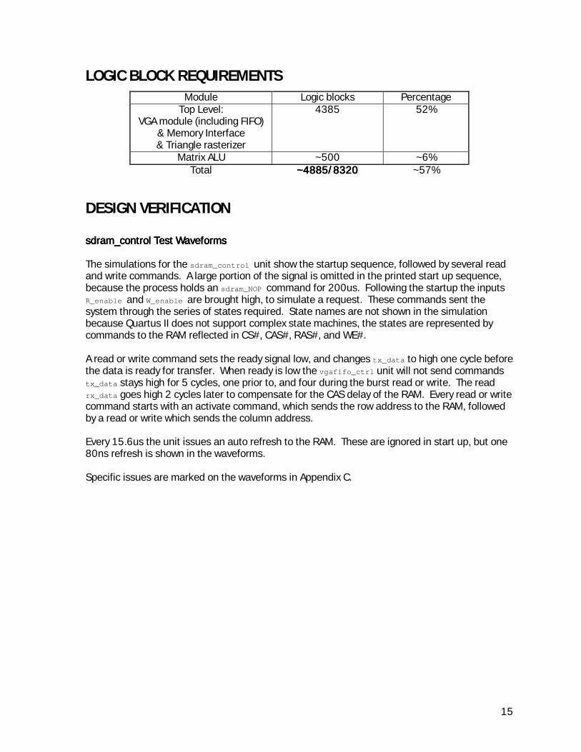
LOGIC BLOCK REQUIREMENTS Module Logic blocks Percentage
Top Level: VGA module (including FIFO)
& Memory Interface & Triangle rasterizer
4385 52%
Matrix ALU ~500 ~6% Total ~4885/8320~4885/8320~4885/8320~4885/8320 ~57%
DESIGN VERIFICATION sdram_control Test Waveformssdram_control Test Waveformssdram_control Test Waveformssdram_control Test Waveforms The simulations for the sdram_control unit show the startup sequence, followed by several read and write commands. A large portion of the signal is omitted in the printed start up sequence, because the process holds an sdram_NOP command for 200us. Following the startup the inputs R_enable and W_enable are brought high, to simulate a request. These commands sent the system through the series of states required. State names are not shown in the simulation because Quartus II does not support complex state machines, the states are represented by commands to the RAM reflected in CS#, CAS#, RAS#, and WE#. A read or write command sets the ready signal low, and changes tx_data to high one cycle before the data is ready for transfer. When ready is low the vgafifo_ctrl unit will not send commands tx_data stays high for 5 cycles, one prior to, and four during the burst read or write. The read rx_data goes high 2 cycles later to compensate for the CAS delay of the RAM. Every read or write command starts with an activate command, which sends the row address to the RAM, followed by a read or write which sends the column address. Every 15.6us the unit issues an auto refresh to the RAM. These are ignored in start up, but one 80ns refresh is shown in the waveforms. Specific issues are marked on the waveforms in Appendix C.
16
vgaout Test Waveformsvgaout Test Waveformsvgaout Test Waveformsvgaout Test Waveforms The simulations for the vgaout module run through an entire horizontal line. Buffer data request signals are asserted every 8 pixels because the incoming word length is 64 bits, so that one word is actually 8 pixels. The horizontal count increases and controls the timing of the video signals. The pixel data is active (sVideoOnH = 1) from 0 < sHCount < 639, or for 640 pixels. The horizontal sync signal is sent (Horiz_Sync = 0) when 683 < sHCount < 730, or for 46 pixels. These timings are specified above and in the file vgaout_defs.vhd. A new line of pixels is requested from the VGA FIFO about 40 clock cycles before the beginning of a new line (when sHCount is 776). This allows the FIFO to retrieve just under 40 x 2 x 8 = 640 pixels (i.e. the entire line) before it is needed. It retrieves 64 bits per data transfer, and is clocked twice as quickly as the VGA module. Some overhead is lost due to SDRAM control signals, but the buffer should be nearly completely full by the time the data is required. These waveforms are shown in Appendix C. Frame_buffer_test waveformsFrame_buffer_test waveformsFrame_buffer_test waveformsFrame_buffer_test waveforms These waveforms show the operation of the vgaout and SDRAM units acting together. The memory startup has been omitted for space. Speed InformationSpeed InformationSpeed InformationSpeed Information Max Speed: 50MHz Critical Path: Off Chip to SDRAM, (internally, the critical path is the rasterizer algorithm) Solution: Difficult to say at this point. Data and address outputs to the RAM are registered. More time will be dedicated to testing if other portions are completed with time to spare. Experiments and Characterization Device Size/Speed ExperimentsDevice Size/Speed ExperimentsDevice Size/Speed ExperimentsDevice Size/Speed Experiments When the SDRAM module is compiled for different FPGA architectures, a change in speed is observed: Apex 20K160EFC484-1 (closest model to the 20K200 available in the Web edition of Quartus) fmax = 297/6400 (4%) Area = 91.84MHz Apex 20K30ETC144-1 fmax = 94.45MHz Area = 297/1200 (24%) It can be seen that even the newer, larger chips can have slower fmaxes, likely do to longer routing to pins and other areas of the chip. There is still a trade off between speed and area. Data Mask ExperimentsData Mask ExperimentsData Mask ExperimentsData Mask Experiments When performing write masking we often had difficulty determining what was previously in memory and what had been written correctly. To reduce confusion a special .sof which wrote the entire framebuffer to pink was created. Therefore, prior to testing later experiments with the data mask, the entire frame was blanked to pink, so it could be determined what was being masked.

17
SDRAM Speed ExperimentsSDRAM Speed ExperimentsSDRAM Speed ExperimentsSDRAM Speed Experiments Due to odd and inconsistent behaviours with the SDRAM setup and hold violations several speeds were tried. Although 55MHz was originally stable, after more functionality was added, the clock was reduced to 50MHz. All cores can currently run at 50MHz.
Slope Calculation Speed/Area TradeoffsSlope Calculation Speed/Area TradeoffsSlope Calculation Speed/Area TradeoffsSlope Calculation Speed/Area Tradeoffs In order to meet the target clock frequency, the slope calculation engine was heavily pipelined. It’s main component is an lpm_divide unit. The “LPM_PIPELINE” parameter was tested with the following values and results:
Pipeline depth fmax Logic cells used 8 45.9 MHz 1045 (12%)
15 57.6 MHz 1377 (16%) 17 75.1 MHz 1421 (17%)
This experiment was performed while the target clock frequency was 66 MHz. After relaxing the timing requirements, the slope calculation pipeline was shortened to conserve logic resources. TRIAGE The most essential modules of the project are the VGA output routine, the SDRAM controller (i.e. the z-buffer and frame buffer), and the triangle rasterizer. The transformation engine and user-input modules are the least important features, and may be omitted if time or space are limited.
18
REFERENCES General 3dfx Interactive. 1999. SST-1 (aka Voodoo GraphicsTM) High Performance Graphics Engine for 3D Game
Acceleration. Double Description Polyhedral Algorithm, Skorobohatyj, G. 1999. accessed February 13, 2002 at URL
http://elib.zib.de/pub/Packages/mathprog/polyth/dda/. Floating Point Operations in VHDL, 1996. accessed February 24, 2002 at URL http://www-
old.ics.uci.edu/pub/hlsynth/HLSynth95/HLSynth95/complete/. Opencores Projects, Multiple authors, 2002. accessed January 5, 2002 at URL http://www.opencores.org Altera Corp. 2001. APEX 20K200 Pin-out table. Altera Corp. 2001. Using the ClockLock & ClockBoost PLL Features on Apex Devices. Altera Corp. 2001. Nios Embedded Processor Development Board Data Sheet. Tessier, T. and T. Bishop. 1996. Using VHDL Abstract Data Types to Design a High Performance 3-D
Graphics Pipeline, Talcian Corporation (pdf) Matrix Arithmetic Calculator, Aggarwal, A., U. Al-Shiraida and M. Panech. 1998. accessed Jan. 12, 2002 at
URL http://www.ee.ualberta.ca/~elliott/ee552/projects/1998f/matrix_calculator. 3-D Rendering Acceleration (newsgroup post). Gray, J. accessed Jan. 10, 2002 at URL
http://www.fpgacpu.org/usenet/render.html. Triangle Rasterization 3D Basics: AGP, T&L, & Texturing, Smith, T. (FiringSquad) 2001. accessed January 12, 2002 at URL
http://firingsquad.gamers.com/guides/3dbasics/default.asp 3D Basics 2: Anti-aliasing, RAM and Z, Smith, T. 2001. accessed January 12, 2002 at URL
http://firingsquad.gamers.com/guides/3dbasics2/; accessed Jan. 18, 2002. Graphics Gems (C Graphic Algorithm Collection), Haines, E. accessed January 20, 2002 at URL
http://www.graphicsgems.org Rasterization Algorithms (lecture notes), Levoy, M. 2001. accessed February 27, 2002 at URL
http://graphics.stanford.edu/courses/cs248-01/scan/scan1.html Memory Altera Corp. 2000. Altera SDR SDRAM Controller White Paper Enhanced Memory Systems. 2001. Preliminary Datasheet - 144-pin SODIMM. Mobel Electronics 2001. Datasheet - 144-pin SODIMM. Wrobel, H., Snyder, J. (Motorola) 2001. MPC8xx SDRAM Interface. (Application Note AN2066ID). IEEE Standard for Floating Point Arithmetic, 1999. Pittsburgh Supercomputing Center, Carnegie Mellon
University. accessed February 10, 2002 at URL http://www.psc.edu/general/software/packages/ieee/ieee.html.
Using a CPLD to Implement an SDRAM Controller, Novak, M. 1997. accessed February 8, 2002 at URL http://archives.e-insite.net/archives/ednmag/reg/1997/060597/12df_04.htm#Table%201.
VGA Out VGA Signal Generation with the XS Board, XESS Corp. 2000. accessed January 8, 2002 at URL
http://xess.com/appnotes/vga.pdf. Viewsonic E771 Datasheet, Viewsonic Corp. 1999, accessed March 6, 2002 from URL
http://www.viewsonic.com/pdf/e771.pdf. Hamblen, J. razzle.vhd. Koles, Z. 2002. EEBE 540 Course Notes.

19
APPENDIX A Design Hierarchy

20

21
APPENDIX B VHDL Code & Index

22
Index of VHDL Code
memory_defs.vhd..............................................................................Error! Bookmark not defined.Error! Bookmark not defined.Error! Bookmark not defined.Error! Bookmark not defined. sdram_control.vhd.............................................................................Error! Bookmark not defined.Error! Bookmark not defined.Error! Bookmark not defined.Error! Bookmark not defined. vgaout_defs.vhd ................................................................................Error! Bookmark not defined.Error! Bookmark not defined.Error! Bookmark not defined.Error! Bookmark not defined. vgaout.vhd..........................................................................................Error! Bookmark not defined.Error! Bookmark not defined.Error! Bookmark not defined.Error! Bookmark not defined. vgafifo.vhd..........................................................................................Error! Bookmark not defined.Error! Bookmark not defined.Error! Bookmark not defined.Error! Bookmark not defined. vgafifo_ctrl.vhd ..................................................................................Error! Bookmark not defined.Error! Bookmark not defined.Error! Bookmark not defined.Error! Bookmark not defined. pll2x.vhd.............................................................................................Error! Bookmark not defined.Error! Bookmark not defined.Error! Bookmark not defined.Error! Bookmark not defined. rasterizer.vhd.....................................................................................Error! Bookmark not defined.Error! Bookmark not defined.Error! Bookmark not defined.Error! Bookmark not defined. rasterizer_ctrl.vhd..............................................................................Error! BoError! BoError! BoError! Bookmark not defined.okmark not defined.okmark not defined.okmark not defined. raster_vars_reg.vhd...........................................................................Error! Bookmark not defined.Error! Bookmark not defined.Error! Bookmark not defined.Error! Bookmark not defined. frame_buffer_test.vhd ......................................................................Error! Bookmark not defined.Error! Bookmark not defined.Error! Bookmark not defined.Error! Bookmark not defined. transform.vhd ....................................................................................Error! Bookmark not defined.Error! Bookmark not defined.Error! Bookmark not defined.Error! Bookmark not defined. Write_fifo.vhd.....................................................................................Error! Bookmark not defined.Error! Bookmark not defined.Error! Bookmark not defined.Error! Bookmark not defined. triangle_sorter.vhd ............................................................................Error! Bookmark not defined.Error! Bookmark not defined.Error! Bookmark not defined.Error! Bookmark not defined. triangle_buffer_defs.vhd...................................................................Error! Bookmark not defined.Error! Bookmark not defined.Error! Bookmark not defined.Error! Bookmark not defined. slope_calc.vhd ...................................................................................Error! Bookmark not defined.Error! Bookmark not defined.Error! Bookmark not defined.Error! Bookmark not defined. shift_reg_8x8.vhd..............................................................................Error! Bookmark not defined.Error! Bookmark not defined.Error! Bookmark not defined.Error! Bookmark not defined.
vgaout_top.vhd is the top-level entity of the VGA output module. The vgafifo, vgafifo_ctrl, pll2x and vgaout modules are sub-entities. Vgaout_defs contains constants for these files. Sdram_control is the SDRAM controller, memory_manager is the memory request arbiter and rasterizer is the triangle rasterization module. The rasterization process is controlled using raster_vars_reg and rasterizer_control The arbitrary location write is handeled in write_fifo, and rasterization and tranformaton is done in rasterizer and transform respeactively. Pll2x.vhd is Altera’s phase locked loop code for 50.00MHz clock. Slope_calc is a dedicated slope unit for transformations and rasterization, as well as calculating all x, y and z slopes.

23
APPENDIX C
Simulation Waveforms

24
Index of Test Waveforms
sdram_control Test Waveforms................................................................................................. 25 vgaout Test Waveforms.............................................................................................................. 26 Frame_buffer_test waveforms .................................................................................................. 27 Rasterizer waveforms................................................................................................................. 28

25
sdram_control Test Waveformssdram_control Test Waveformssdram_control Test Waveformssdram_control Test Waveforms The simulations for the sdram_control unit show the startup sequence, followed by several read and write commands. A large portion of the signal is omitted in the printed start up sequence, because the process holds an sdram_NOP command for 200us. Following the startup the inputs R_enable and W_enable are brought high, to simulate a request. These commands sent the system through the series of states required. State names are not shown in the simulation because Quartus II does not support complex state machines, the states are represented by commands to the RAM reflected in CS#, CAS#, RAS#, and WE#. A read or write command sets the ready signal low, and changes tx_data to high one cycle before the data is ready for transfer. When ready is low the memory_manager unit will not send commands tx_data stays high for 5 cycles, one prior to, and four during the burst read or write. The read tx_data goes high 2 cycles later to compensate for the CAS delay of the RAM. Every read or write command starts with an activate command, which sends the row address to the RAM, followed by a read or write which sends the column address. Every 15.6us the unit issues an auto refresh to the RAM. These are ignored in start up, but one 80ns refresh is shown in the waveforms.

26
vgaout Test Waveformsvgaout Test Waveformsvgaout Test Waveformsvgaout Test Waveforms The simulations for the vgaout module run through an entire horizontal line. Buffer data request signals are asserted every 8 pixels because the incoming word length is 64 bits, so that one word is actually 8 pixels. The horizontal count increases and controls the timing of the video signals. The pixel data is active (sVideoOnH = 1) from 0 < sHCount < 639, or for 640 pixels. The horizontal sync signal is sent (Horiz_Sync = 0) when 683 < sHCount < 730, or for 46 pixels. These timings are specified above and in the file vgaout_defs.vhd. A new line of pixels is requested from the VGA FIFO about 40 clock cycles before the beginning of a new line (when sHCount is 776). This allows the FIFO to retrieve just under 40 x 2 x 8 = 640 pixels (i.e. the entire line) before it is needed. It retrieves 64 bits per data transfer, and is clocked twice as quickly as the VGA module. Some overhead is lost due to SDRAM control signals, but the buffer should be nearly completely full by the time the data is required.
27
Frame_buffer_test waveformsFrame_buffer_test waveformsFrame_buffer_test waveformsFrame_buffer_test waveforms The frame buffer test waveforms are a combination of the previous two simulated units. The following waveforms show the until blanking the memory after the memory start up. Since it needs to do this 640x480 /32 times we cannot show the whole blank, but it can be seen to works.

28
Rasterizer waveforRasterizer waveforRasterizer waveforRasterizer waveformsmsmsms

29
APPENDIX D Schematics

30
Figure Figure Figure Figure 4444: VGA output Schematic: VGA output Schematic: VGA output Schematic: VGA output Schematic
31
APPENDIX E Datasheets
Related Documents