S. Yan, EE382M-14 Lecture 3 1 EE382M-14 CMOS Analog Integrated Circuit Design Lecture 3, MOS Capacitances Small Signal Models, and Passive Components MOS Capacitances n + n + p + p - substrate L eff L D L drawn B (bulk) S (source) G (gate) D (drain) MOS transistor capacitance types: • Depletion capacitance (pn junction capacitance) • Gate-channel or gate-substrate capacitance • Gate-source and gate-drain overlap capacitance

Welcome message from author
This document is posted to help you gain knowledge. Please leave a comment to let me know what you think about it! Share it to your friends and learn new things together.
Transcript

S. Yan, EE382M-14 Lecture 3 1
EE382M-14 CMOS Analog Integrated Circuit Design
Lecture 3, MOS Capacitances Small Signal Models, and Passive Components
MOS Capacitances
n+ n+p+
p- substrate
LeffLD
Ldrawn
B (bulk) S (source)G (gate) D (drain)
MOS transistor capacitance types:
• Depletion capacitance (pn junction capacitance) • Gate-channel or gate-substrate capacitance • Gate-source and gate-drain overlap capacitance
S. Yan, EE382M-14 Lecture 3 2
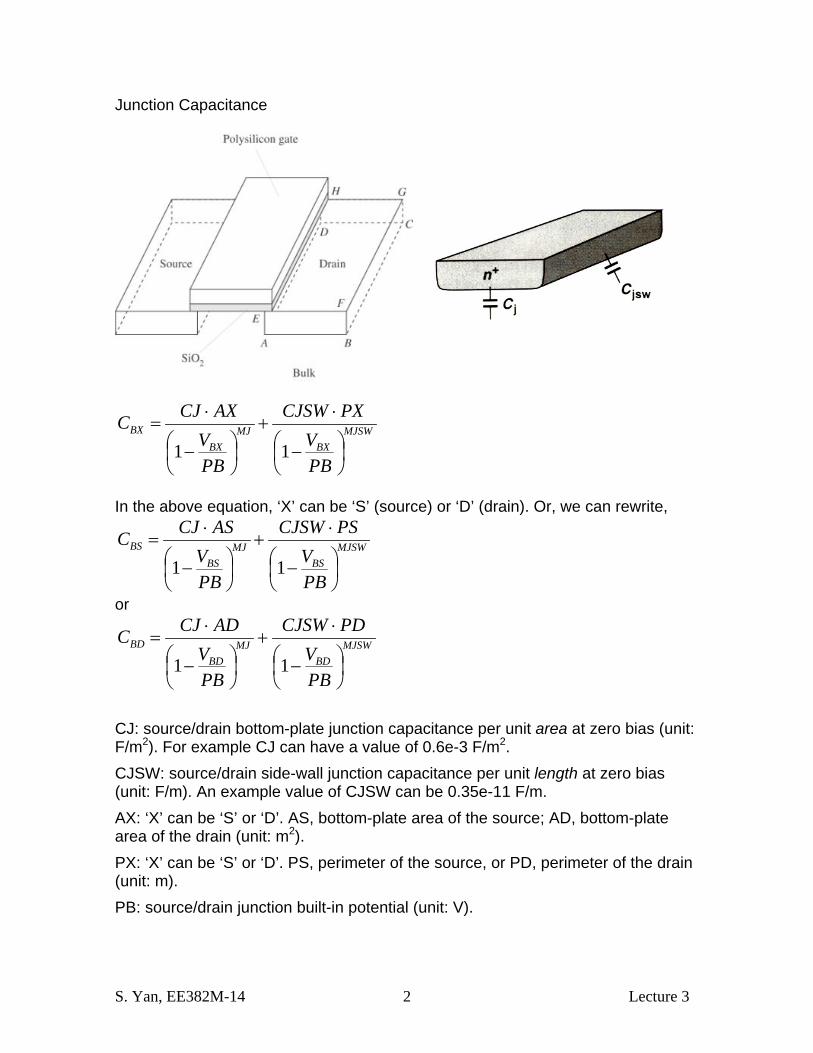
Junction Capacitance
MJSWBX
MJBX
BX
PBV
PXCJSW
PBV
AXCJC⎟⎠⎞
⎜⎝⎛ −
⋅+
⎟⎠⎞
⎜⎝⎛ −
⋅=
11
In the above equation, ‘X’ can be ‘S’ (source) or ‘D’ (drain). Or, we can rewrite,
MJSWBS
MJBS
BS
PBV
PSCJSW
PBV
ASCJC⎟⎠⎞
⎜⎝⎛ −
⋅+
⎟⎠⎞
⎜⎝⎛ −
⋅=
11
or
MJSWBD
MJBD
BD
PBV
PDCJSW
PBV
ADCJC⎟⎠⎞
⎜⎝⎛ −
⋅+
⎟⎠⎞
⎜⎝⎛ −
⋅=
11
CJ: source/drain bottom-plate junction capacitance per unit area at zero bias (unit: F/m2). For example CJ can have a value of 0.6e-3 F/m2. CJSW: source/drain side-wall junction capacitance per unit length at zero bias (unit: F/m). An example value of CJSW can be 0.35e-11 F/m. AX: ‘X’ can be ‘S’ or ‘D’. AS, bottom-plate area of the source; AD, bottom-plate area of the drain (unit: m2). PX: ‘X’ can be ‘S’ or ‘D’. PS, perimeter of the source, or PD, perimeter of the drain (unit: m). PB: source/drain junction built-in potential (unit: V).
S. Yan, EE382M-14 Lecture 3 3
MJ: exponent of the source/drain bottom-plate junction capacitance. MJ may have a value as 0.5. MJSW: exponent of the source/drain side-wall junction capacitance. Gate-Channel and Gate-Substrate Capacitance
Cut-off Triode Saturation Gate-channel 0 CoxWL 2/3⋅CoxWL
Gate-substrate ⎟⎟⎠
⎞⎜⎜⎝
⎛+
WLCWLx
oxsi
d 11ε
+CGB,ov CGB,ov CGB,ov
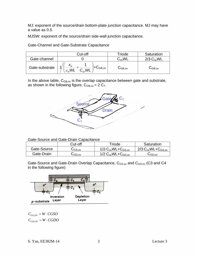
In the above table, CGB,ov is the overlap capacitance between gate and substrate, as shown in the following figure, CGB,ov = 2 C7.
C7
C7GateSource
Drain
Gate-Source and Gate-Drain Capacitance
Cut-off Triode Saturation Gate-Source CGS,ov 1/2⋅CoxWL+CGS,ov 2/3⋅CoxWL+CGS,ov Gate-Drain CGD,ov 1/2⋅CoxWL+CGD,ov CGD,ov
Gate-Source and Gate-Drain Overlap Capacitance, CGS,ov and CGD,ov (C3 and C4 in the following figure)
CGSOWC OVGS ⋅=, CGDOWC OVGD ⋅=,

S. Yan, EE382M-14 Lecture 3 4
where CGSO and CGDO are the gate-source and gate-drain overlap capacitance per unit width (unit: F/m) in Spice Level 1 and Level 2 models. For example CGSO and CGDO can be 0.4e-9 F/m. Variation of gate-source and gate-drain capacitance [allen02]
VGS varying
VDS constant
C1+2C7
C3+C1(C1=2/3⋅Cox⋅W⋅L)
C3+1/2⋅C1or C4+1/2⋅C1
C3 or C4
2C7

S. Yan, EE382M-14 Lecture 3 5
Passive Components Capacitors [allen02] Options
• poly-diffusion capacitor • poly-poly capacitor • metal-metal capacitor
n+
p- substrate
SiO2poly
_______________ capacitor
________________ capacitors
S. Yan, EE382M-14 Lecture 3 6
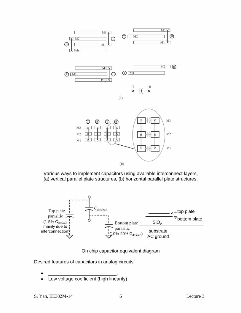
Various ways to implement capacitors using available interconnect layers, (a) vertical parallel plate structures, (b) horizontal parallel plate structures.
substrateAC ground
bottom plate
top plate
SiO2(1-5% Cdesiredmainly due to
interconnection) (10%-20% Cdesired)
On chip capacitor equivalent diagram
Desired features of capacitors in analog circuits
• __________________________. • Low voltage coefficient (high linearity)

S. Yan, EE382M-14 Lecture 3 7
• Low parasitic capacitance • Low temperature dependence • High capacitance per unit area
AMIS 0.5um process capacitance parameters
CAPACITANCE PARAMETERS N+ P+ POLY POLY2 M1 M2 M3 N_W UNITS Area (substrate) 430 725 85 32 17 11 40 aF/um^2 Area (N+active) 2457 36 17 12 aF/um^2 Area (P+active) 2365 aF/um^2 Area (poly) 873 57 17 10 aF/um^2 Area (poly2) 52 aF/um^2 Area (metal1) 36 14 aF/um^2 Area (metal2) 37 aF/um^2 Fringe (substrate) 328 272 78 60 42 aF/um Fringe (poly) 64 40 29 aF/um Fringe (metal1) 50 36 aF/um Fringe (metal2) 53 aF/um Overlap (N+active) 197 aF/um Overlap (P+active) 229 aF/um
From http://www.mosis.org/cgi-bin/cgiwrap/umosis/swp/params/ami-c5/t49m-params.txt Resistors Poly resistors are frequently used in high performance analog circuits. Resistors of diffusion and well have large voltage coefficients.

S. Yan, EE382M-14 Lecture 3 8
On chip resistor options, (a) __________ resistor, (b) __________ (most frequently used) resistor, (c) ___________ resistor
Desired features of resistors in analog circuits
• ________________________. • Low voltage coefficient (high linearity) • Low parasitic capacitance • Low temperature dependence • Suitable resistance per square
WLRRR squarecontact += 2*
AMIS 0.5um process resistance parameters
PROCESS PARAMETERS N+ P+ POLY PLY2_HR POLY2 M1 M2 UNITS Sheet Resistance 83.7 105.9 22.3 990 43.4 0.09 0.09 ohms/sq Contact Resistance 67.2 152.9 16.0 29.1 0.84 ohms Gate Oxide Thickness 141 angstrom PROCESS PARAMETERS M3 N\PLY N_W UNITS Sheet Resistance 0.05 836 829 ohms/sq Contact Resistance 0.85 ohms
From http://www.mosis.org/cgi-bin/cgiwrap/umosis/swp/params/ami-c5/t49m-params.txt

S. Yan, EE382M-14 Lecture 3 9
Layout of Analog Integrated Circuits The design flow of analog integrated circuits
Project definition and specifications
Architecture selection, definition, and system level
simulation
Schematic design and simulation
Layout
Parasitic extraction and post-layout simulation
Fabrication of the prototype chip
Experimental results
General layout considerations The layout of integrated circuits defines the _________________ that appear on the ___________ used in fabrication.

S. Yan, EE382M-14 Lecture 3 10
Photomask and photolithography
Layout of a MOS transistor

S. Yan, EE382M-14 Lecture 3 11
Layout rules or design rules Layout rules or design rules are a set of rules that guarantee successful fabrication
of integrated circuits despite various ____________ in each step of the
processing.
Minimum width
The width of the geometries defined on a mask must exceed a minimum value. For example, if a polysilicon rectangle is too narrow, it may suffer from a large local resistance or even break. Minimum spacing As an example, if 2 polysilicon lines are placed too close, they may be shorted. Minimum enclosure The n-well or the p+ implant must surround the transistor with sufficient margin to make sure that the device is contained within. Below is an example of enclosure rule for poly and metal surrounding a contact.
W
S

S. Yan, EE382M-14 Lecture 3 12
Minimum extension As an example, the poly gate must have a minimum extension beyond the well to ensure that the transistor functions properly at the edge of well. Please check the following webpage for MOSIS design rules, http://www.mosis.org/Technical/Designrules/scmos/scmos-main.html Example: design rules for poly layer
SCMOS Layout Rules - Poly
Lambda Rule Description
SCMOS SUBM DEEP
3.1 Minimum width 2 2 2
3.2 Minimum spacing over field 2 3 3
3.2.a Minimum spacing over active 2 3 4
3.3 Minimum gate extension of active 2 2 2.5
3.4 Minimum active extension of poly 3 3 4
3.5 Minimum field poly to active 1 1 1
S. Yan, EE382M-14 Lecture 3 13
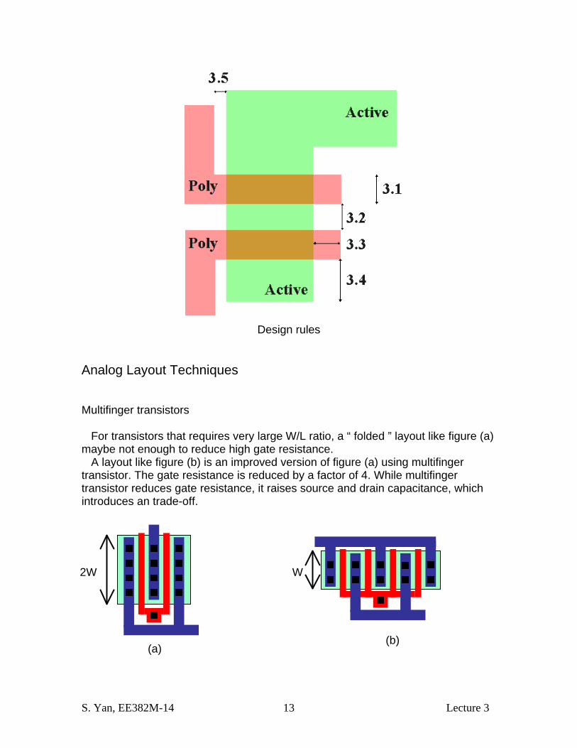
Design rules
Analog Layout Techniques Multifinger transistors For transistors that requires very large W/L ratio, a “ folded ” layout like figure (a) maybe not enough to reduce high gate resistance. A layout like figure (b) is an improved version of figure (a) using multifinger transistor. The gate resistance is reduced by a factor of 4. While multifinger transistor reduces gate resistance, it raises source and drain capacitance, which introduces an trade-off.
(a)
2W
(b)
W

S. Yan, EE382M-14 Lecture 3 14
Symmetry and matching 1) Interdigitized (common centriod) layout For process variation in local area, we can assume that the gradient of the variation is described as: bmxy += Assume component A ,which is composed of units A1 and A2, should be twice the size of component B. For a layout of (a) we have :
22)(21
21
3
21
3
2
1
≠+
++=
+
+=+=
+=
bmxbxxm
BAA
bmxBbmxA
bmxA
For a layout like (b) we have :
22)(21
21
2
31
2
3
1
=+
++=
+
+=+=
+=
bmxbxxm
BAA
bmxBbmxAbmxA
y
x
A1
A2
B
A1
B
A2
(a)
(b)
2x 3x1x

S. Yan, EE382M-14 Lecture 3 15
We call a layout like (b) a common-centroid layout.
2) Using dummy transistors This is an improved version of the layout above. Two dummy transistors are added to the left and right sides. On the layout above, transistor A sees different ambient environment to the left and to the right. Dummy transistors improves the matching between transistor A and B by providing similar environment to the circuit that is on the boundary of a layout.
Dummy Dummy
½ Transistor A ½ Transistor ATransistor B
AG BG
BAS ,
AD
BD
An Example of common centroid layout
S. Yan, EE382M-14 Lecture 3 16
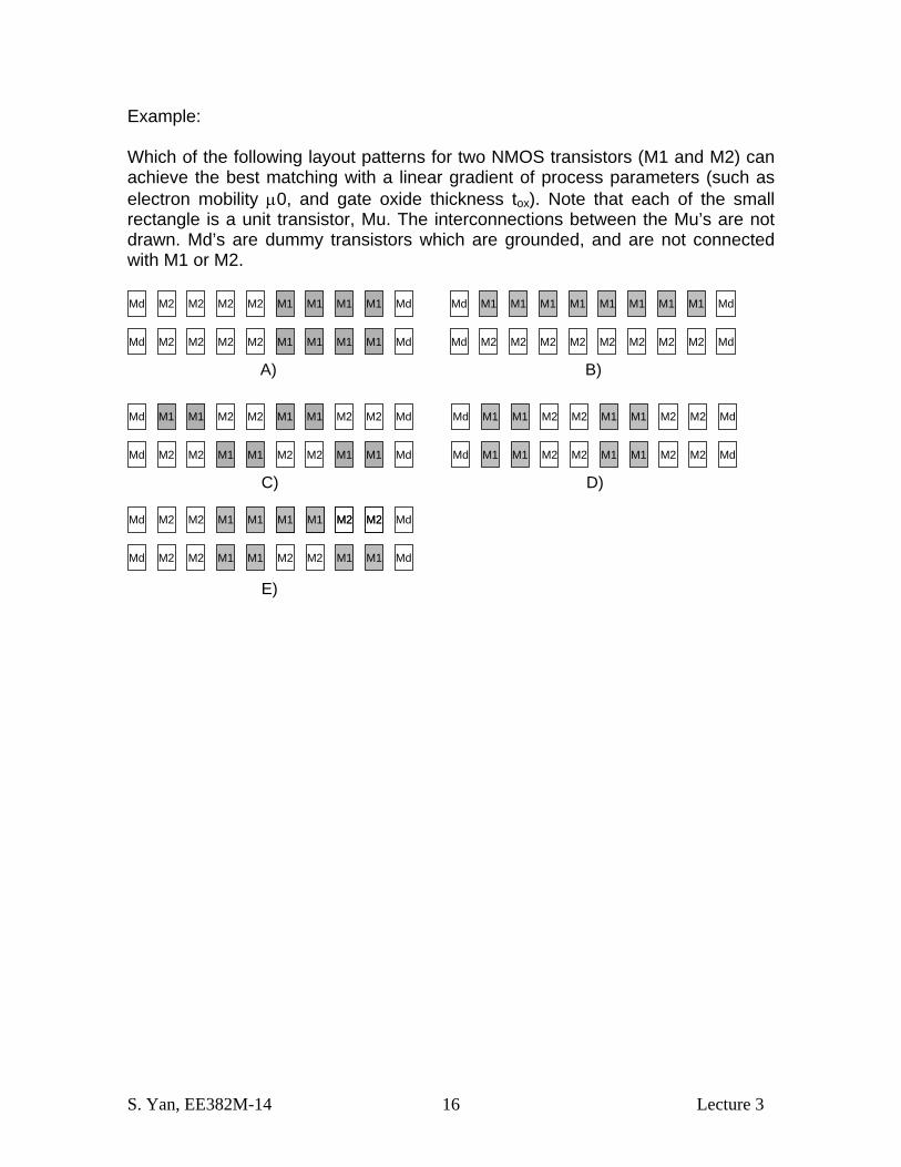
Example: Which of the following layout patterns for two NMOS transistors (M1 and M2) can achieve the best matching with a linear gradient of process parameters (such as electron mobility µ0, and gate oxide thickness tox). Note that each of the small rectangle is a unit transistor, Mu. The interconnections between the Mu’s are not drawn. Md’s are dummy transistors which are grounded, and are not connected with M1 or M2.
M2 M2 M1 M1
M2 M2 M1 M1
Md
Md
Md
Md
M1 M1 M2 M2 M1 M1 M2 M2
M1M1M2M2M1M1M2M2
Md
Md
Md
Md
M1 M1 M2 M2 M1 M1 M2 M2
M1 M1 M2 M2 M1 M1 M2 M2
Md
Md
Md
Md
M1 M1 M1 M1 M1 M1 M1 M1
M2 M2 M2 M2 M2 M2 M2 M2
Md
Md
Md
Md
M2 M2 M2 M2 M1 M1 M1 M1
M2 M2 M2 M2 M1 M1 M1 M1
Md
Md
Md
Md
A) B)
C) D)
E)
M2M2M1M1 M2M2M1M1
M2 M2 M1 M1
S. Yan, EE382M-14 Lecture 3 17
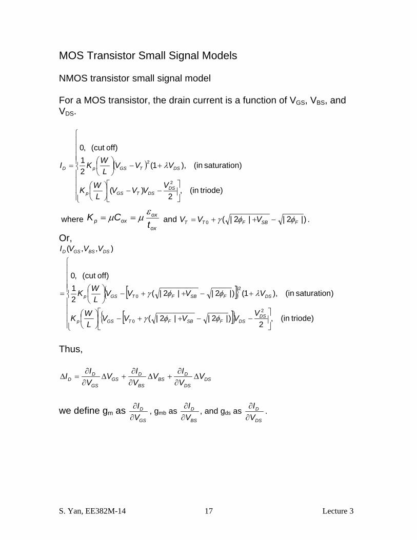
MOS Transistor Small Signal Models NMOS transistor small signal model For a MOS transistor, the drain current is a function of VGS, VBS, and VDS.
( )
⎪⎪⎪⎪
⎩
⎪⎪⎪⎪
⎨
⎧
⎥⎦
⎤⎢⎣
⎡−−⎟
⎠⎞
⎜⎝⎛
+−⎟⎠⎞
⎜⎝⎛=
triode) (in ,2
)(
)saturation (in ),1(21
off) (cut ,0
2
2
DSDSTGSp
DSTGSpD
VVVVL
WK
VVVL
WKI λ
where ox
oxoxp t
CK εµµ == and )|2||2|(0 FSBFTT VVV φφγ −++= .
Or,
[ ]{ }
[ ]{ }⎪⎪⎪⎪
⎩
⎪⎪⎪⎪
⎨
⎧
⎥⎦
⎤⎢⎣
⎡−−++−⎟
⎠⎞
⎜⎝⎛
+−++−⎟⎠⎞
⎜⎝⎛=
triode) (in ,2
)|2||2|(
)saturation (in ),1()|2||2|(21
off) (cut ,0
),,(
2
0
2
0
DSDSFSBFTGSp
DSFSBFTGSp
DSBSGSD
VVVVVL
WK
VVVVL
WK
VVVI
φφγ
λφφγ
Thus,
DSDS
DBS
BS
DGS
GS
DD V
VIV
VIV
VII ∆
∂∂
+∆∂∂
+∆∂∂
=∆
we define gm as
GS
D
VI
∂∂ , gmb as
BS
D
VI
∂∂ , and gds as
DS
D
VI
∂∂ .
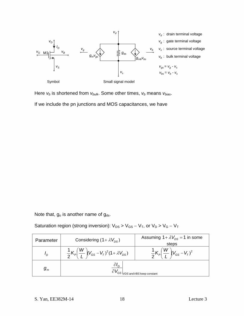
S. Yan, EE382M-14 Lecture 3 18
gdsgmvgs gmbvbs
vd
vg
vs
vb
vd : drain terminal voltage
vg : gate terminal voltage
vs : source terminal voltage
vb : bulk terminal voltage
vgs = vg - vs
vbs = vb - vs
M1vG
vD
vS
vB
Symbol Small signal model
ID
Here vb is shortened from vbulk. Some other times, vb means vbias. If we include the pn junctions and MOS capacitances, we have Note that, go is another name of gds. Saturation region (strong inversion): VDS > VGS − VT, or VD > VG − VT
Parameter Considering ( DSVλ+1 ) Assuming 11 =+ DSVλ in some steps
DI )()( DSTGSP VVVL
WK λ+−⎟⎠⎞
⎜⎝⎛ 1
21 2 2
21 )( TGSP VV
LWK −⎟
⎠⎞
⎜⎝⎛
mg constant keep and VBSVDSGS
D
VI
∂∂

S. Yan, EE382M-14 Lecture 3 19
))(( DSTGSP VVVL
WK λ+−⎟⎠⎞
⎜⎝⎛ 1 )( TGSP VV
LWK −⎟
⎠⎞
⎜⎝⎛
)( DSPD VL
WKI λ+⎟⎠⎞
⎜⎝⎛ 12 ⎟
⎠⎞
⎜⎝⎛
LWKI PD2
TGS
D
VVI−
2 TGS
D
VVI−
2
constant keep and constant keep and VDSVGSBS
T
T
D
VDSVGSBS
D
VV
VI
VI
∂∂
∂∂
=∂∂
mbg
mgη where SBFBS
T
VVV
+=
∂∂
−=|| φ
γη22
constant keep and VBSVGSDS
D
VI
∂∂
λ2
21 )( TGSP VV
LWK −⎟
⎠⎞
⎜⎝⎛ N/A dsg
DS
D
VI
λλ
+1 DIλ
Triode region (strong inversion): VDS < VGS − VT, or VD < VG − VT
Parameter Considering ( DSVλ+1 ) * Assuming 11 =+ DSVλ in some steps
DI )()( DSDS
DSTGSp VVVVVL
WK λ+⎥⎦
⎤⎢⎣
⎡−−⎟
⎠⎞
⎜⎝⎛ 1
2
2
⎥⎦
⎤⎢⎣
⎡−−⎟
⎠⎞
⎜⎝⎛
2
2DS
DSTGSpVVVV
LWK )(
constant keep and VBSVDSGS
D
VI
∂∂
mg
)( DSDSP VVL
WK λ+⎟⎠⎞
⎜⎝⎛ 1 DSP V
LWK ⎟
⎠⎞
⎜⎝⎛
constant keep and constant keep and VDSVGSBS
T
T
D
VDSVGSBS
D
VV
VI
VI
∂∂
∂∂
=∂∂
mbg
mgη where SBFBS
T
VVV
+=
∂∂
−=|| φ
γη22
dsg constant keep and VBSVGSDS
D
VI
∂∂

S. Yan, EE382M-14 Lecture 3 20
})(
){(
⎥⎦
⎤⎢⎣
⎡−−+
−−⎟⎠⎞
⎜⎝⎛
2
2DS
DSTGS
DSTGSP
VVVV
VVVL
WK
λ
(rarely used)
)( DSTGSP VVVL
WK −−⎟⎠⎞
⎜⎝⎛
* )( DSVλ+1 is added in the equation )()( DSDS
DSTGSp VVVVVL
WK λ+⎥⎦
⎤⎢⎣
⎡−−⎟
⎠⎞
⎜⎝⎛ 1
2
2
to
bridge the equations in triode and saturation regions. Note that
ox
oxoxp t
CK εµµ == and )||||( FSBFTT VVV φφγ 220 −++=
( )TGS VV − has different names in different books, VOV (over drive voltage), VON, Vdsat (or Vds(sat), D-S saturation voltage). We mix using all of these terms. PMOS transistor small signal model
gdsgmvgs gmbvbs
vs
vg
vd
vb
vd : drain terminal voltage
vg : gate terminal voltage
vs : source terminal voltage
vb : bulk terminal voltage
vgs = vg - vs
vbs = vb - vs
M1vG
vS
vD
vB
Symbol Small signal model
ID
You may notice that we use the same small signal model for both PMOS and NMOS transistors. We assume for both NMOS and PMOS transistors, the reference direction of the drain current is the direction that current flows into the transistor from drain terminal. Please pay attention to the signs of in SPICE model parameters for NMOS and PMOS transistors.
Parameter VT KP λ NMOS + + + PMOS − − +
S. Yan, EE382M-14 Lecture 3 21
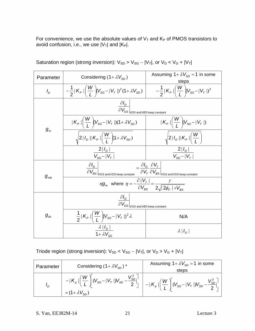
For convenience, we use the absolute values of VT and KP of PMOS transistors to avoid confusion, i.e., we use |VT| and |KP|. Saturation region (strong inversion): VSD > VSG − |VT|, or VD < VG + |VT|
Parameter Considering ( SDVλ+1 ) Assuming 11 =+ SDVλ in some steps
DI )(|)|(|| SDTSGP VVVL
WK λ+−⎟⎠⎞
⎜⎝⎛− 1
21 2 2
21 |)|(|| TSGP VV
LWK −⎟
⎠⎞
⎜⎝⎛−
constant keep and VBSVDSGS
D
VI
∂∂
)|)(|(|| SDTSGP VVVL
WK λ+−⎟⎠⎞
⎜⎝⎛ 1 |)|(|| TSGP VV
LWK −⎟
⎠⎞
⎜⎝⎛
)(|||| SDPD VL
WKI λ+⎟⎠⎞
⎜⎝⎛ 12 ⎟
⎠⎞
⎜⎝⎛
LWKI PD ||||2
mg
||||
TSG
D
VVI
−2
||||
TSG
D
VVI
−2
constant keep and constant keep and VDSVGSBS
T
T
D
VDSVGSBS
D
VV
VI
VI
∂∂
∂∂
=∂∂
mbg
mgη where BSFBS
T
VVV
+=
∂∂
−=||
||φ
γη22
constant keep and VBSVGSDS
D
VI
∂∂
λ2
21 |)|(|| TSGP VV
LWK −⎟
⎠⎞
⎜⎝⎛ N/A dsg
SD
D
VI
λλ+1
|| || DIλ
Triode region (strong inversion): VSD < VSG − |VT|, or VD > VG + |VT|
Parameter Considering ( SDVλ+1 ) * Assuming 11 =+ SDVλ in some steps
DI )(
|)|(||
SD
SDSDTSGp
V
VVVVL
WK
λ+×
⎥⎦
⎤⎢⎣
⎡−−⎟
⎠⎞
⎜⎝⎛−
12
2
⎥⎦
⎤⎢⎣
⎡−−⎟
⎠⎞
⎜⎝⎛−
2
2SD
SDTSGpVVVV
LWK |)|(||
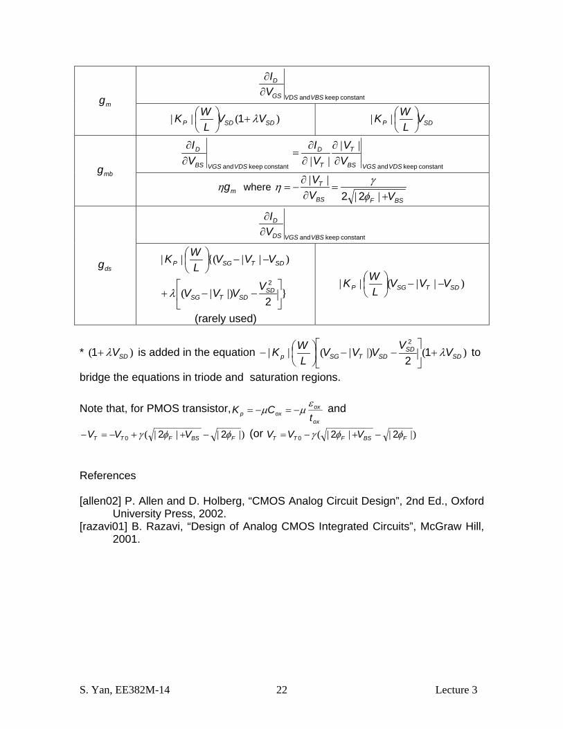
S. Yan, EE382M-14 Lecture 3 22
constant keep and VBSVDSGS
D
VI
∂∂
mg
)(|| SDSDP VVL
WK λ+⎟⎠⎞
⎜⎝⎛ 1 SDP V
LWK ⎟
⎠⎞
⎜⎝⎛||
constant keep and constant keep and VDSVGSBS
T
T
D
VDSVGSBS
D
VV
VI
VI
∂∂
∂∂
=∂∂ ||
||
mbg
mgη where BSFBS
T
VVV
+=
∂∂
−=||
||φ
γη22
constant keep and VBSVGSDS
D
VI
∂∂
dsg
}|)|(
)||{(||
⎥⎦
⎤⎢⎣
⎡−−+
−−⎟⎠⎞
⎜⎝⎛
2
2SD
SDTSG
SDTSGP
VVVV
VVVL
WK
λ
(rarely used)
)||(|| SDTSGP VVVL
WK −−⎟⎠⎞
⎜⎝⎛
* )( SDVλ+1 is added in the equation )(|)|(|| SDSD
SDTSGp VVVVVL
WK λ+⎥⎦
⎤⎢⎣
⎡−−⎟
⎠⎞
⎜⎝⎛− 1
2
2
to
bridge the equations in triode and saturation regions.
Note that, for PMOS transistor,ox
oxoxp t
CK εµµ −=−= and
)||||( FBSFTT VVV φφγ 220 −++−=− (or )||||( FBSFTT VVV φφγ 220 −+−=
References [allen02] P. Allen and D. Holberg, “CMOS Analog Circuit Design”, 2nd Ed., Oxford
University Press, 2002. [razavi01] B. Razavi, “Design of Analog CMOS Integrated Circuits”, McGraw Hill,
2001.
Related Documents