Professor N Cheung, U.C. Berkeley Lecture 13 EE143 S06 1 Vacuum Basics 1. Units – 1 atmosphere = 760 torr = 1.013x10 5 Pa – 1 bar = 10 5 Pa = 750 torr – 1 torr = 1 mm Hg – 1 mtorr = 1 micron Hg – 1Pa = 7.5 mtorr = 1 newton/m 2 – 1 torr = 133.3 Pa 2. Ideal Gas Law: PV = NkT – k = 1.38E-23 Joules/molecule –K = 1.37E-22 atm cm 3 /K – N = # of molecules – T = absolute temperature in K – [Note] At T = 300 K ; kT = 3.1E-20 torr-liter 1

Welcome message from author
This document is posted to help you gain knowledge. Please leave a comment to let me know what you think about it! Share it to your friends and learn new things together.
Transcript

Professor N Cheung, U.C. Berkeley
Lecture 13EE143 S06
1
Vacuum Basics
1. Units– 1 atmosphere = 760 torr = 1.013x10⁵ Pa– 1 bar = 105 Pa = 750 torr– 1 torr = 1 mm Hg– 1 mtorr = 1 micron Hg – 1Pa = 7.5 mtorr = 1 newton/m2
– 1 torr = 133.3 Pa
2. Ideal Gas Law: PV = NkT– k = 1.38E-23 Joules/molecule –K
= 1.37E-22 atm cm3/K– N = # of molecules– T = absolute temperature in K– [Note] At T = 300 K ; kT = 3.1E-20 torr-liter
1

Professor N Cheung, U.C. Berkeley
Lecture 13EE143 S06
2
For mixture of non-reactive gases in a common vessel, each gas exerts its pressure independent of others.
Ptotal = P1 + P2 + … + PN (Total P = Sum of partial pressure)Ntotal = N1 + N2 + … + NNP1V = N1kTP2V = N2kT...................PNV = NNkT
3. Dalton’s Law of Partial Pressure

Professor N Cheung, U.C. Berkeley
Lecture 13EE143 S06
3
4. Average Molecular Velocity
v = (8kT/πm)1/2
where m = molecular weight of gas molecule
5. Mean Free Path of molecular collision
λ = 1
2 πd2o n
where n = molecular density = N/V,do = molecular diameter
[Note] For air at 300 °K, λ = 6.6
P( in Pa) = 0.05
P( in torr)with λ in mm
Assumes Maxwell-Boltzman Velocity Distribution

Professor N Cheung, U.C. Berkeley
Lecture 13EE143 S06
4
6. Impingement Rate, Φ
Φ = n v
4 = # of molecules striking unit surface /unit time.
= 3.5×10²² × PmT
in #/cm2-secwith P in torr, m in amu
[Note] For air at 300 °K ; Φ(in #/cm2 -sec) = 3.8×10²⁰ ⋅P
Example Calculation : Contamination from Residual Vacuum
For a residual vacuum of 10-6 torr, Φ = 4 × 10¹⁴/cm2-secIf each striking molecule sticks to the surface, the equivalent deposition rate of the residual gas is ~ 1/3 of a monolayer of solid per second.

Professor N Cheung, U.C. Berkeley
Lecture 13EE143 S06
5
Pressure (Torr)
Tim
e to
form
a m
onol
ayer
(sec
)
Impi
ngm
entR
ate
(Mol
ecul
es/c
m2 s
)
Mea
n fr
ee P
ath
(mm
)
At 25oC
M
I
P
1 meter!
1 µm/min
Vacuum Basics (Cont.)
ResidualVacuum
Plasma Processing
CVD

Professor N Cheung, U.C. Berkeley
Lecture 13EE143 S06
6
Thin Film Deposition
substratefilm
Applications:Metalization (e.g. Al, TiN, W, silicide)Poly-Sidielectric layers; surface passivation.
EvaporationSputtering
Reactive Sputtering
Chemical Vapor DepositionLow Pressure CVD
Plasma Enhanced CVD
Physical Methods Chemical Methods

Professor N Cheung, U.C. Berkeley
Lecture 13EE143 S06
7
(1) Evaporation Deposition
Al film
wafer
Al vapor
Al
hot heatingboat (e.g. W)
I
electronsource
crucible is water cooled
Al vapor
=PmkT2π
P P eHkT=
−
0∆
Vapor PressureEvaporation Rate (max)
m=molecular weight of vapor molecule
Log P
1/T
e
Vacuum Torr< 10 -5

Professor N Cheung, U.C. Berkeley
Lecture 13EE143 S06
8
Vapor Pressure versus Temperature

Professor N Cheung, U.C. Berkeley
Lecture 13EE143 S06
9
Basic Properties of Plasma
• The bulk of plasma contains equal concentrations of ions and electrons.
• Electric potential is ≈ constant inside bulk of plasma. The voltage drop is mostly across the sheath regions.
• Plasma used in IC processing is a “weak” plasma, containing mostly neutral atoms/molecules. Degree of ionization is ≈ 10-3 to 10-6.

Professor N Cheung, U.C. Berkeley
Lecture 13EE143 S06
10Source: www.icknowledge.com

Professor N Cheung, U.C. Berkeley
Lecture 13EE143 S06
11
DiffusionFlux
DriftFlux
E ≠ 0
E ~ 0

Professor N Cheung, U.C. Berkeley
Lecture 13EE143 S06
12
Al
(2) Sputtering Deposition
Al AlAr+
Deposited Al film
Al target
Ar plasma
waferheat substrate to ~ 300oC (optiona12l)
Negative Bias ( kV)
⋅
I
Gas Pressure 1-10 m TorrDeposition rate =
≅sputtering yield
ion current
constant I S• •
Ar+
Example:DC plasma
12

Professor N Cheung, U.C. Berkeley
Lecture 13EE143 S06
13Source: www.icknowledge.com

Professor N Cheung, U.C. Berkeley
Lecture 13EE143 S06
14

Professor N Cheung, U.C. Berkeley
Lecture 13EE143 S06
15
S ≡# of ejected target atoms
incoming ion.
0.1 < S < 30
Al
Al
Al
Ar
Sputtering Yield S
Professor N Cheung, U.C. Berkeley
Lecture 13EE143 S06
16
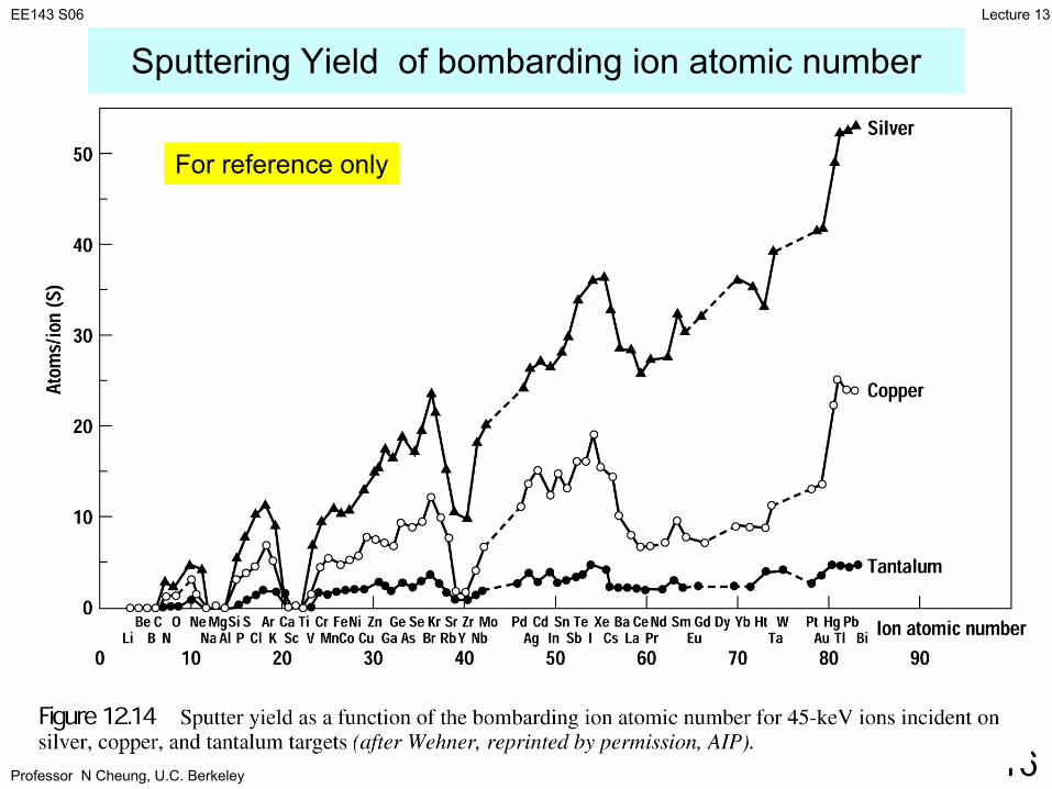
Sputtering Yield of bombarding ion atomic number
For reference only

Professor N Cheung, U.C. Berkeley
Lecture 13EE143 S06
17
The Sputtering Yield with incidence angle

Professor N Cheung, U.C. Berkeley
Lecture 13EE143 S06
18
Ar+
Aflux
Bflux
AxBy
targetFilm has same composition of target at steady state.
Because SA ≠ SB, Target surface will acquire a composition Ax’By’ at steady state.
Sputtering of Compound Targets

Professor N Cheung, U.C. Berkeley
Lecture 13EE143 S06
19
Target
AxBy
Deposited Film on substrate
AxBy
AxBy
Ax’By
’
Ax’By
’
t=t1
t=t2Difference betweent2 and t1 must becomposition depositedon substrate
Bulk target composition
Proof

Professor N Cheung, U.C. Berkeley
Lecture 13EE143 S06
20
Reactive Sputtering
• Sputter a Ti target with a nitrogen plasma
Ti Target
N2 plasma
Ti, N2+
TiN
Example: Formation of TiN
Substrate
Note: TiN is a metallic compoundwith a golden color. It is used frequentlyin ICs as a metallic conductor. When sandwiched between two thin films, it can also be used as a “diffusion barrier” to block thin-film reactions

Professor N Cheung, U.C. Berkeley
Lecture 13EE143 S06
21
Radio Frequency Plasma Generation
For reference only
•More efficient plasma generation•Needed if substrate is electricallyinsulating

Professor N Cheung, U.C. Berkeley
Lecture 13EE143 S06
22

Professor N Cheung, U.C. Berkeley
Lecture 13EE143 S06
23
Thickness Uniformity with various PVD sources
(i) Point-like Source
(ii) Plane-like small-area SourceF
θsurface
θ
wafer
isotropic
•Ideal situation•Flux F leaving source surface isindependent of θ (isotropic source)
F
•Flux F leaving surface ∝ cos θExample: E-beam evaporation

Professor N Cheung, U.C. Berkeley
Lecture 13EE143 S06
24
Let F = emission flux from sourceTherefore receiving flux F’ at a distance r from source = F/ r2
If the receiving surface is making an angle φ with respect to the F’ vectorThickness deposited ∝ F’ cos φ = F cos φ / r2
Film Thickness Deposition on Wafer
F
F’
source
waferφr
Professor N Cheung, U.C. Berkeley
Lecture 13EE143 S06
25
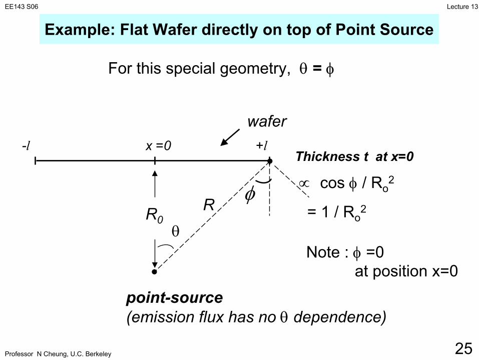
wafer-l +lx =0
R0R
point-source(emission flux has no θ dependence)
φ
Thickness t at x=0
∝ cos φ / Ro2
= 1 / Ro2
Note : φ =0 at position x=0
For this special geometry, θ = φ
θ
Example: Flat Wafer directly on top of Point Source

Professor N Cheung, U.C. Berkeley
Lecture 13EE143 S06
26
( ) ( )
( )( )
23
2
01
0
3
coscos
3
22
0
0
0
220
220
−
+=
+=
=+=
=
+=
+=
Rl
lR
Rxt
lxt
R
RlRlR
θφ
x=0 x=+l
Thickness t at position x= +l ∝ cos φ / R2

Professor N Cheung, U.C. Berkeley
Lecture 13EE143 S06
27
Example: Plane-like Source & Spherical Receiving Surface
θ
φθ
φ
θ
θφθ
2cos21
coscos21
cos'waferonThickness
cos21'fluxReceiving
cos flux F Emission
r
r
Fr
F
∝
∝
⋅∝
⋅∝
∝=
Since cos θ = (r/2)/R
Thickness∴ ∝ = constant(1/r2) (r2/4R2)
waferR
R
r
plane-source
θ
φ F ’

Professor N Cheung, U.C. Berkeley
Lecture 13EE143 S06
28
Step Coverage Problem with PVD
• Both evaporation and sputtering have directional fluxes.
wafer
step
filmFlux
film
“geometricalshadowing”

Professor N Cheung, U.C. Berkeley
Lecture 13EE143 S06
29
stepfilm
“self-shadowing”
t=t1
t=0 t=t11 244444 344444
shadowing distance
t=0

Professor N Cheung, U.C. Berkeley
Lecture 13EE143 S06
30

Professor N Cheung, U.C. Berkeley
Lecture 13EE143 S06
31
Film Thinningat stepsstep step
wafer
“key hole”
Key Hole Formation
Thinner film depositionat steps

Professor N Cheung, U.C. Berkeley
Lecture 13EE143 S06
32
Sputtering Target
Methods to Minimize Step Coverage Problems
• Rotate + Tilt substrate during deposition• Elevate substrate temperature (enhance
surface diffusion)• Use large-area deposition source

Professor N Cheung, U.C. Berkeley
Lecture 13EE143 S06
33
Dip Photoresist in Chlorobenzene to slow down developingrate of surface layer .
Surface layer treated by chlorobenzene
Photoresist
Directional Deposition Flux
film
Patterning of deposited layer using directional deposition.
Lift-off Technique

Professor N Cheung, U.C. Berkeley
Lecture 13EE143 S06
34
Sputtering Target
Profile due to one small-area source
Superposition of all small-area sources
Sputtering Target
Profile due to one small-area source
Superposition of all small-area sources
•Better lateral thickness uniformityArea of sputtering target can be made much larger than that of an evaporating source. A larger area can be considered as a superposition of many small-area sources. By adding the flux from all the sources, a large area source will provide better lateral film deposition uniformity on wafer.
•For multi-component thin films, sputtering gives better composition control using compound targets. Evaporation depends on vapor pressure of various vapor components and is difficult to control.
Advantages of Sputtering over Evaporation
Related Documents