EE143 EE143 Microfabrication Technology Professor: Ali Javey Professor: Ali Javey [email protected] 506 Cory Hall (510) 643-7263 GSIs: Reinaldo Vega (Head GSI): [email protected] Jaewon Jang: jessjjang@gmail com Jaewon Jang: jessjjang@gmail.com Chen Lu: [email protected] Philip Chen: [email protected] Web Page: TBA EE143 – Ali Javey Slide 0-1

Welcome message from author
This document is posted to help you gain knowledge. Please leave a comment to let me know what you think about it! Share it to your friends and learn new things together.
Transcript

EE143EE143Microfabrication Technology
Professor: Ali JaveyProfessor: Ali [email protected] Cory Hall(510) 643-7263( )
GSIs:Reinaldo Vega (Head GSI): [email protected] Jang: jessjjang@gmail comJaewon Jang: [email protected] Lu: [email protected] Chen: [email protected]
Web Page: TBA
EE143 – Ali Javey Slide 0-1

Schedule• Lectures: Tue/Thu, 2pm-3:30pm• Labs (218 Cory) –
– Tu 10:00-1:00P– W 10:00-1:00P– W 2:00-5:00P– Th 9:00-12:00P– F 9:00-12:00P– F 2:00-5:00P
• Note the Friday afternoon section is not listed in telebears.LAB SECTIONS WILL BEGIN ON September 1LAB SECTIONS WILL BEGIN ON September 1.
• Office Hours:Ali (C ll 06)– Ali Javey (Cory Hall, 506)Wednesdays, 10-11 am
– TAs (TBD)
EE143 – Ali Javey Slide 0-2

Reading Material• Primary Text:
Introduction To Microelectronic FabricationR. C. JaegerPrentice Hall
• Reference Texts:Semiconductor Device FundamentalsR F Pi tR. F. PierretAddison Wesley
Device Electronics for Integrated CircuitsR. S. Muller and T. I. KaminsWiley
EE143 – Ali Javey Slide 0-3
Wiley

GradingL b t– Laboratory• Includes quizzes, lab work, and reports
– Homeworks
35% We will follow the EECS grading guidelines for this class:
“A typical GPA for courses in the upperHomeworks• ~3 HW sets will be assigned throughout the semester
• You must work on your own
5%A typical GPA for courses in the upper
division is 2.9. (This GPA would result, for example, from 23% A's, 50% B's, 20% C's, 5% D's, and 2% F's.) A class whose GPA falls outside the range 2 7– Tests (2)
• ~75 minutes each• given periodically per schedule 30%
whose GPA falls outside the range 2.7 -3.1 should be considered atypical. A typical GPA for basic prerequisite upper division courses (EECS 104A, EECS 105 CS 150 CS 153) is 2 7 with GPA's• One sheet of notes allowed
• No makeups
Final E amination
105, CS 150, CS 153) is 2.7 with GPA s outside the range 2.5 - 2.9 considered atypical.”
htt // b k l d /P li i / d di ht l– Final Examination• Three sheets of notes allowed 30%
http://www.eecs.berkeley.edu/Policies/ugrad.grading.shtml
EE143 – Ali Javey Slide 0-4

Grading
• Laboratory (35% of the total grade)- Lab attendance: 10 pts (5% of the total grade). Each absence results in -2 pts. E h l t lt i 1 t St d t i i l b tt d d f 0 tEach lateness results in -1 pt. Students receiving a lab attendance grade of 0 pts or less will automatically fail the course. Make-up lab sections are allowed (student will be attending a different lab section for that week), however, prior written request must be submitted to Professor Javey. Students attending pre-q y g papproved make-up sections will not lose points. Note that being unprepared, unwilling to participate in the lab activities, and/or not following the safety procedures will result in losing lab attendance points.
L b Q i (5% f h l d ) Th ill b i f ( d)- Lab Quizzes: (5% of the total grade). They will be given often (unannounced) at the beginning of each lab.- Lab Report 1: 100 pts (15% of the total grade). For every day that it is turned in late you will lose 20 pts We will not collect after 4 days past the deadlinein late, you will lose 20 pts. We will not collect after 4 days past the deadline.-Lab Report 2: 100 pts (10% of the total grade). For every day that it is turned in late, you will lose 20 pts. We will not collect after 4 days past the deadline.
EE143 – Ali Javey Slide 0-5

Course Information• Prerequisites:
– EE40/E100 and Physics 7B or equivalent• Course Description• Course Description
– EE143 teaches the fundamentals of integrated-circuit (IC) fabrication and surface-micromachining technology, giving the student a basic understanding of IC and micromachining processes and the effect of g g pprocessing choices on device performance. Students learn to use process simulation tools and also fabricate and characterize devices in the laboratory. This lecture part will cover the processing techniques and design methodologies of microfabrication We will discuss theand design methodologies of microfabrication. We will discuss the process modules: lithography, thermal oxidation, diffusion, ion implantation, etching, thin-film deposition, epitaxy, metallization. The second part of the course will cover process simulation, layout design p p y grules, MOS, IC, and MEMS process integration. The laboratory part of the course will provide students opportunities to have hands-on experience to fabricate and characterize a NMOS chip with simple MEMS components
EE143 – Ali Javey Slide 0-6
MEMS components.

Course Schedule
Introduction to Materials and Processing (1-2 weeks)Photolithography (1 week)Photolithography (1 week)Etching (1 week)Oxidation (1 week)Deposition (1 week)Diffusion (1 week)Ion Implantation (1 week)Metallization/CMP (1 week)Simulation/Layout (1 week)Process Integration (1 week)Process Integration (1 week)Introduction to Devices (2 weeks)Nanolithography and Nanofabrication (1 week)
EE143 – Ali Javey Slide 0-7

Laboratory Information• We do our best to limit lab size to 12 people; as a result, your telebears
enrollment is not a guarantee of being assigned to a lab.
• You MUST send an email to Professor Javey ([email protected]) by this Friday 10pm including the following information:
– 1) Full Name– 2) Major– 3) Year (Jr., Sr., Grad student, etc.)
4) Rank list of preferred lab sections in descending order of preference (i.e., 1st
choice, 2nd choice…)– 5) List of any lab sections that you CANNOT attend
• Failure to send an email may result in you being dropped from the course, even if you are registered on telebears.
Fi l l b i t ill b t t i il PLEASE ENSURE• Final lab assignment will be sent to you via email. PLEASE ENSURE THAT YOUR EMAIL ADDRESS ON TELEBEARS IS CORRECT, SINCE THIS WILL BE USED FOR OFFICIAL CORRESPONDENCE!!!
EE143 – Ali Javey Slide 0-8

Lab Safety
Week of 9/1• Mandatory Lab attendance required• Mandatory Lab attendance required
Y ill h l b i t ti i d• You will have a lab orientation session, and will have to pass a safety quiz before you are officially enrolled in this courseare officially enrolled in this course.
Y MUST tt d th l b i t hi h• You MUST attend the lab session to which you are assigned.
EE143 – Ali Javey Slide 0-9

Course Structure – Lab and Lecture• You learn the theories in class; you practice them in
lab• You are going to make:
– resistors, diodes, MOS-cap– bipolar transistor, MOS-transistor, …– some MEMS structures, like bimorphs, …
B h d f h h ld h l• By the end of the semester, you should have learnt– basic lab techniques
h t t f b i ti i t– how to operate some fabrication equipment– how to characterize the devices you made
EE143 – Ali Javey Slide 0-10

The EE143 Chip
EE143 – Ali Javey Slide 0-11

Lab Cleanliness• only enter the clean room fully gowned
– hair net + lab coat + glove + shoe net + safety goggles
d NOT t h h i l / i t ith b• do NOT touch chemicals / equipment with bare hands
• always handle wafers with tweezers and trays (unless told otherwise)(unless told otherwise)
• wash hands before and after entering the lab (why??)– before: so as not to contaminate wafers or
equipment– after: avoid chemicals being indigested
• 3rd week, GSIs will demonstrate how to clean kmasks
• 4th week, GSIs will demonstrate how to piranha-clean wafers
EE143 – Ali Javey Slide 0-12

Lab Safety• do NOT enter the lab when GSI aren’t present• know all the emergency exits (ask the GSIs to
show you)show you)• know where to find the MSDS
– under the whiteboard in characterization room• know where to find the closet water sources,
shower, eye wash, sink• ask whenever not clear• do NOT try things out without permission• NO eating, drinking, playing, etc. inside the lab
hi i h l b b d if• Things in the lab can be dangerous if not carefully handled. Be sure to respect the chemicals.
EE143 – Ali Javey Slide 0-13

Chemical Handling• wear protective gear when handling corrosive chemicals
– face shield, chemical apron, chemical gloves, respirator if necessaryy
• check glove for holes• check pH of unknown spillage, label everything
i h i l H SO HF l i t h TMAH• corrosive chemicals: H2SO4, HF, aluminum etch, TMAH• wash and rinse the exposed body parts with water for >
15mins• add acids to water, not the other way around• handle wet chemicals only at sinks, acid on right, others on
left sideleft side
EE143 – Ali Javey Slide 0-14

Chemical Handling (cont’d)• HF:
– be very very careful– HF will penetrate your body and attack your skeletal
system; once you feel it it is already eating your bones!!!system; once you feel it, it is already eating your bones!!!– apply calcium gluconate if exposure is suspected– use only plastic beakers for HF (why??)
• H2SO4:– very painful, severely burns– add H2O2 to H2SO4 to prepare piranha– do not carry the beaker around after mixing (HOT!!)– use only glass beakers for piranha (why??)use only glass beakers for piranha (why??)
• Chemicals used in the lab are often harmful. Don’t breathe and avoid exposure if possible.
• Use teflon-ware when handling wafers in acids. Be f l th t fl t d t h ld th fcareful, those teflon tweezers do not hold the wafers very
well!!
EE143 – Ali Javey Slide 0-15

Chemical Disposal• organic chemicals are discarded in designated
containers• NOTE: in this lab, photoresist (PR) is also
dumped down the drain.• do NOT mix organic wastes with acids (why??)
– can cause fire or even explosion
• do NOT mix acids and bases
EE143 – Ali Javey Slide 0-16

Lab Floor PlanNote: Not drawn to scale
EE143 – Ali Javey Slide 0-17

EE143 Overview• Microfabrication Principles for IC• Hands-on Fabrication and Testing of IC Devices
EE143 – Ali Javey Slide 0-18

Fabricated Structures• Using a series of planar processing steps, it is possible to
create sophisticated 3D electrical and mechanical structures.
EE143 – Ali Javey Slide 0-19

Electrical Functionality / Characterization• The resulting structures may be characterization
electrically or mechanically
17-stage Ring Oscillator
EE143 – Ali Javey Slide 0-20
g g

Introduction to Si ProcessingIntroduction to Si ProcessingEE143 in one day

Silicon Device Fabrication Technology
Over 1019 transistors (or 1,000,000,000 for every person in the world) are manufactured every year.
Variations of this versatile technology are used for flat-panel displays, micro-electro-mechanical systems ( ) d hi f i(MEMS), and even DNA chips for DNA screening...

Terminology
SSI (Small Scale Integration) – few transistorsMSI (Medium Scale Integration) – hundreds
LSI (Large Scale Integration) - thousandsVLSI (Very Large Scale Integration) - millions
ULSI (Ul L S l I i )ULSI (Ultra Large Scale Integration)

Foundry (Fab)• Foundry (also called a fab for fabrication
plant) is used to refer to a factory where p ) ydevices like integrated circuits are manufactured. The central part of a fab is a pcleanroom.
• Note the difference between a fab and a lab.

Cleanroom Standards
Federal Standard Class Limits
CLASSMEASURED PARTICLE SIZE (MICROMETERS)
0.1 0.2 0.3 0.5 5.0
1 35 7.5 3 1 NA
10 350 75 30 10 NA
100 NA 750 300 100 NA
1,000 NA NA NA 1,000 7
10,000 NA NA NA 10,000 70
100,000 NA NA NA 100,000 700
Why do we need cleanrooms?

Introduction to Device Fabrication
Oxidation
Lithography &Etching
Ion Implantationp
Annealing & gDiffusion
D itiDeposition

Oxidation of SiliconSi + O2 → SiO2
Si +2H2O → SiO2 + 2H2
Dry Oxidation :
Wet Oxidation :
Thin oxide
Thick oxide

Oxidation of Silicon
Quartz tube
Si Wafers
Flowcontroller
O2 N2
H2O or TCE(trichloroethylene) Resistance-heated furnace

Lithography
Resist Coating Development
Positive resist Negative resistPhotoresist
Positive resist Negative resist
OxideSi(a)
Deep Ultraviolet Light Si Si(c)
OpticalLens system
Photomask withopaque and
clear patterns
(c)
Exposure Et hi d R i t St i
SiSi(d)
(b)Exposure Etching and Resist Strip(b)

Pattern Transfer–Etchingwet etch dry etch
Isotropic etching Anisotropic etchingphotoresist photoresist
wet etch dry etch
SiO2
(1)
SiO2
(1)(1)
photoresist
(1)
photoresist
SiO2
(2) (2)
SiO2
SiO2
SiO2
(3) (3)

Module: Ion Implantation
Ion Energy~1 keV to200 keV
EE143 – Ali Javey Slide 0-31

What is process integration?• Sequential use of a series of simple process steps or
“modules” to create complex structures
Si waferSi wafer
ProcessingSteps
EE143 – Ali Javey Slide 0-32

The EE143 Lab Process (part I)
EE143 – Ali Javey Slide 0-33
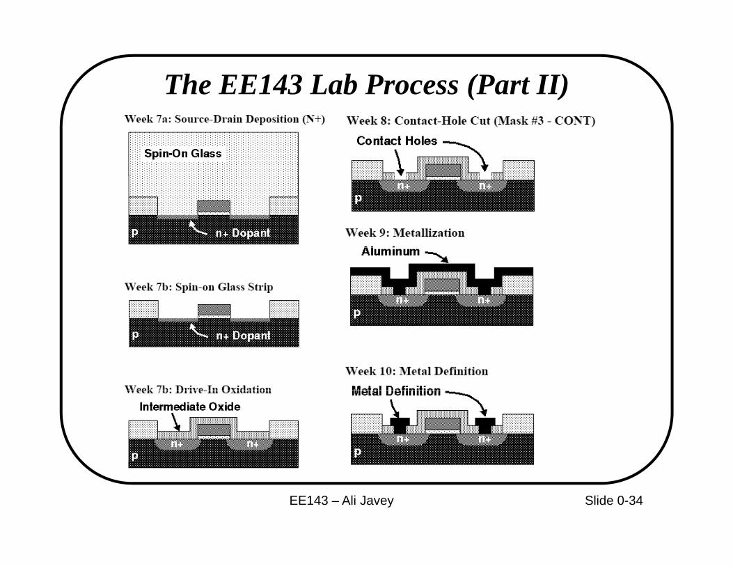
The EE143 Lab Process (Part II)
EE143 – Ali Javey Slide 0-34
Related Documents