EE141 1 gital Integrated Circuits 2nd Combinational Circu Designing Combinationa Designing Combinationa Logic Circuits: Part2 Logic Circuits: Part2 Alternative Logic Form Alternative Logic Form Ratio Logic Ratio Logic Pass-Transistor Pass-Transistor Dynamic Logic Dynamic Logic

EE141 © Digital Integrated Circuits 2nd Combinational Circuits 1 Designing Combinational Logic Circuits: Part2 Alternative Logic Forms: Ratio Logic Pass-Transistor.
Dec 19, 2015
Welcome message from author
This document is posted to help you gain knowledge. Please leave a comment to let me know what you think about it! Share it to your friends and learn new things together.
Transcript

EE1411
© Digital Integrated Circuits2ndCombinational Circuits
Designing CombinationalDesigning CombinationalLogic Circuits: Part2Logic Circuits: Part2Alternative Logic Forms:Alternative Logic Forms:
Ratio LogicRatio LogicPass-TransistorPass-TransistorDynamic LogicDynamic Logic

EE1412
© Digital Integrated Circuits2ndCombinational Circuits
Ratio LogicRatio Logic
VDD
VSS
PDNIn1In2In3
F
RLLoad
VDD
VSS
In1In2In3
F
VDD
VSS
PDNIn1In2In3
F
VSS
PDN
Resistive DepletionLoad
PMOSLoad
(a) resistive load (b) depletion load NMOS (c) pseudo-NMOS
VT < 0
Goal: to reduce the number of devices over complementary CMOS

EE1413
© Digital Integrated Circuits2ndCombinational Circuits
Ratio LogicRatio LogicVDD
VSS
PDN
In1
In2
In3
F
RLLoad
ResistiveN transistors + Load
• VOH = VDD
• VOL = RPN
RPN + RL
• Assymetrical response
• Static power consumption
•
• tpL = 0.69 RLCL

EE1414
© Digital Integrated Circuits2ndCombinational Circuits
Active LoadsActive LoadsVDD
VSS
In1In2In3
F
VDD
VSS
PDN
In1In2In3
F
VSS
PDN
Depletion
LoadPMOSLoad
depletion load NMOS pseudo-NMOS
VT < 0

EE1415
© Digital Integrated Circuits2ndCombinational Circuits
Pseudo-NMOSPseudo-NMOS
VDD
A B C D
FCL
VOH = VDD (similar to complementary CMOS)
kn VDD VTn– VOL
VOL2
2-------------–
kp
2------ VDD VTp– 2=
VOL VDD VT– 1 1kpkn------–– (assuming that VT VTn VTp )= = =
SMALLER AREA & LOAD BUT STATIC POWER DISSIPATION!!!

EE1416
© Digital Integrated Circuits2ndCombinational Circuits
Pseudo-NMOS VTCPseudo-NMOS VTC
0.0 0.5 1.0 1.5 2.0 2.50.0
0.5
1.0
1.5
2.0
2.5
3.0
Vin [V]
Vou
t [V
]
W/Lp = 4
W/Lp = 2
W/Lp = 1
W/Lp = 0.25
W/Lp = 0.5

EE1417
© Digital Integrated Circuits2ndCombinational Circuits
Improved LoadsImproved Loads
A B C D
F
CL
M 1M2 M1 >> M2Enable
VDD
Adaptive Load

EE1418
© Digital Integrated Circuits2ndCombinational Circuits
Even Better Noise ImmunityEven Better Noise Immunity
VDD
VSS
PDN1
Out
VDD
VSS
PDN2
Out
AABB
M1 M2
Differential Cascode Voltage Switch Logic (DCVSL)

EE1419
© Digital Integrated Circuits2ndCombinational Circuits
DCVSL ExampleDCVSL Example
B
A A
B B B
Out
Out
XOR-NXOR gate

EE14110
© Digital Integrated Circuits2ndCombinational Circuits
DCVSL Transient ResponseDCVSL Transient Response
0 0.2 0.4 0.6 0.8 1.0-0.5
0.5
1.5
2.5
Time [ns]
Vol
tage
[V] A B
A B
A,BA,B

EE14111
© Digital Integrated Circuits2ndCombinational Circuits
Pass-Transistor LogicPass-Transistor Logic
• N transistors
• No static consumption
Inpu
ts Switch
Network
OutOut
A
A
B
B

EE14112
© Digital Integrated Circuits2ndCombinational Circuits
Example: AND GateExample: AND Gate
B
B
A
F = AB
0

EE14113
© Digital Integrated Circuits2ndCombinational Circuits
NMOS-Only LogicNMOS-Only Logic
VDD
In
Outx
0.5m/0.25m0.5m/0.25m
1.5m/0.25m
0 0.5 1 1.5 20.0
1.0
2.0
3.0
Time [ns]
Vo
ltage
[V]
xOut
In

EE14114
© Digital Integrated Circuits2ndCombinational Circuits
NMOS-only SwitchNMOS-only Switch
A = 2.5 V
B
C = 2.5 V
CL
A = 2.5 V
C = 2.5 V
BM2
M1
Mn
Threshold voltage loss causesstatic power consumption
VB does not pull up to 2.5V, but 2.5V - VTN
NMOS has higher threshold than PMOS (body effect)

EE14115
© Digital Integrated Circuits2ndCombinational Circuits
NMOS Only Logic: NMOS Only Logic: Level Restoring TransistorLevel Restoring Transistor
M2
M1
Mn
Mr
OutA
B
VDDVDDLevel Restorer
X
• Advantage: Full Swing
• Restorer adds capacitance, takes away pull down current at X
• Ratio problem
EE14116
© Digital Integrated Circuits2ndCombinational Circuits
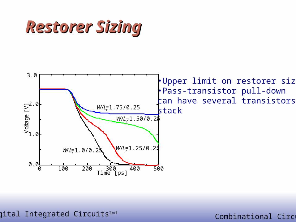
Restorer SizingRestorer Sizing
0 100 200 300 400 5000.0
1.0
2.0
W/Lr =1.0/0.25 W/Lr =1.25/0.25
W/Lr =1.50/0.25
W/Lr =1.75/0.25
Vol
tage
[V]
Time [ps]
3.0•Upper limit on restorer size•Pass-transistor pull-downcan have several transistors in stack
EE14117
© Digital Integrated Circuits2ndCombinational Circuits
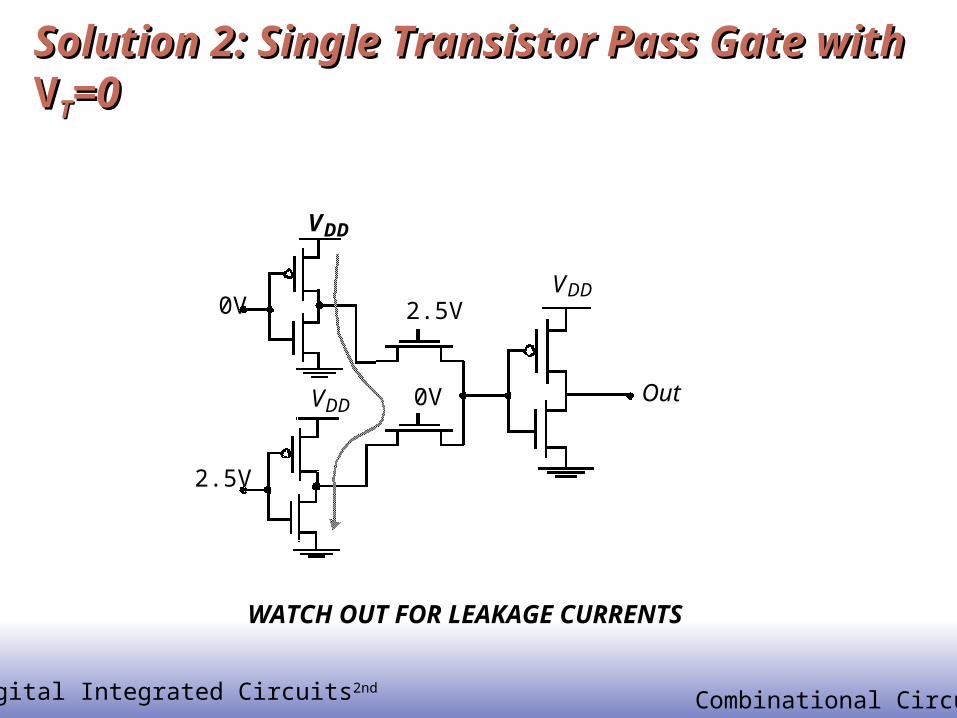
Solution 2: Single Transistor Pass Gate Solution 2: Single Transistor Pass Gate with with VVTT=0=0
Out
VDD
VDD
2.5V
VDD
0V 2.5V
0V
WATCH OUT FOR LEAKAGE CURRENTS

EE14118
© Digital Integrated Circuits2ndCombinational Circuits
Complementary Pass Transistor LogicComplementary Pass Transistor Logic
A
B
A
B
B B B B
A
B
A
B
F=AB
F=AB
F=A+B
F=A+B
B B
A
A
A
A
F=AÝ
F=AÝ
OR/NOR EXOR/NEXORAND/NAND
F
F
Pass-Transistor
Network
Pass-TransistorNetwork
AABB
AABB
Inverse
(a)
(b)

EE14119
© Digital Integrated Circuits2ndCombinational Circuits
Solution 3: Transmission GateSolution 3: Transmission Gate
A B
C
C
A B
C
C
B
CL
C = 0 V
A = 2.5 V
C = 2.5 V

EE14120
© Digital Integrated Circuits2ndCombinational Circuits
Resistance of Transmission GateResistance of Transmission Gate
Vout
0 V
2.5 V
2.5 VRn
Rp
0.0 1.0 2.00
10
20
30
Vout, V
Res
ista
nce
, oh
ms
Rn
Rp
Rn || Rp
EE14121
© Digital Integrated Circuits2ndCombinational Circuits
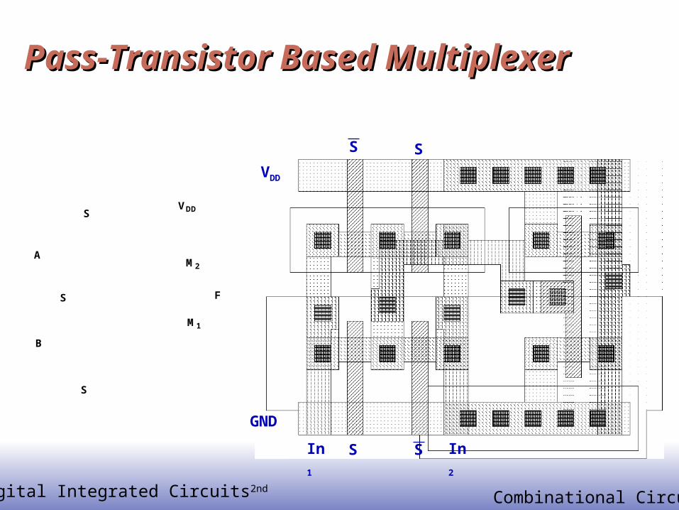
Pass-Transistor Based MultiplexerPass-Transistor Based Multiplexer
AM2
M1
B
S
S
S F
VDD
GND
VDD
In1
In2
S S
S S

EE14122
© Digital Integrated Circuits2ndCombinational Circuits
Transmission Gate XORTransmission Gate XOR
A
B
F
B
A
B
B
M1
M2
M3/M4

EE14123
© Digital Integrated Circuits2ndCombinational Circuits
Delay in Transmission Gate NetworksDelay in Transmission Gate Networks
V1 Vi-1
C
2.5 2.5
0 0
Vi Vi+1
CC
2.5
0
Vn-1 Vn
CC
2.5
0
In
V1 Vi Vi+1
C
Vn-1 Vn
CC
In
ReqReq Req Req
CC
(a)
(b)
C
Req Req
C C
Req
C C
Req Req
C C
Req
C
In
m
(c)

EE14124
© Digital Integrated Circuits2ndCombinational Circuits
Delay OptimizationDelay Optimization

EE14125
© Digital Integrated Circuits2ndCombinational Circuits
Transmission Gate Full AdderTransmission Gate Full Adder
A
B
P
Ci
VDDA
A A
VDD
Ci
A
P
AB
VDD
VDD
Ci
Ci
Co
S
Ci
P
P
P
P
P
Sum Generation
Carry Generation
Setup
Similar delays for sum and carry

EE14126
© Digital Integrated Circuits2ndCombinational Circuits
Dynamic Dynamic LogicLogic
EE14127
© Digital Integrated Circuits2ndCombinational Circuits
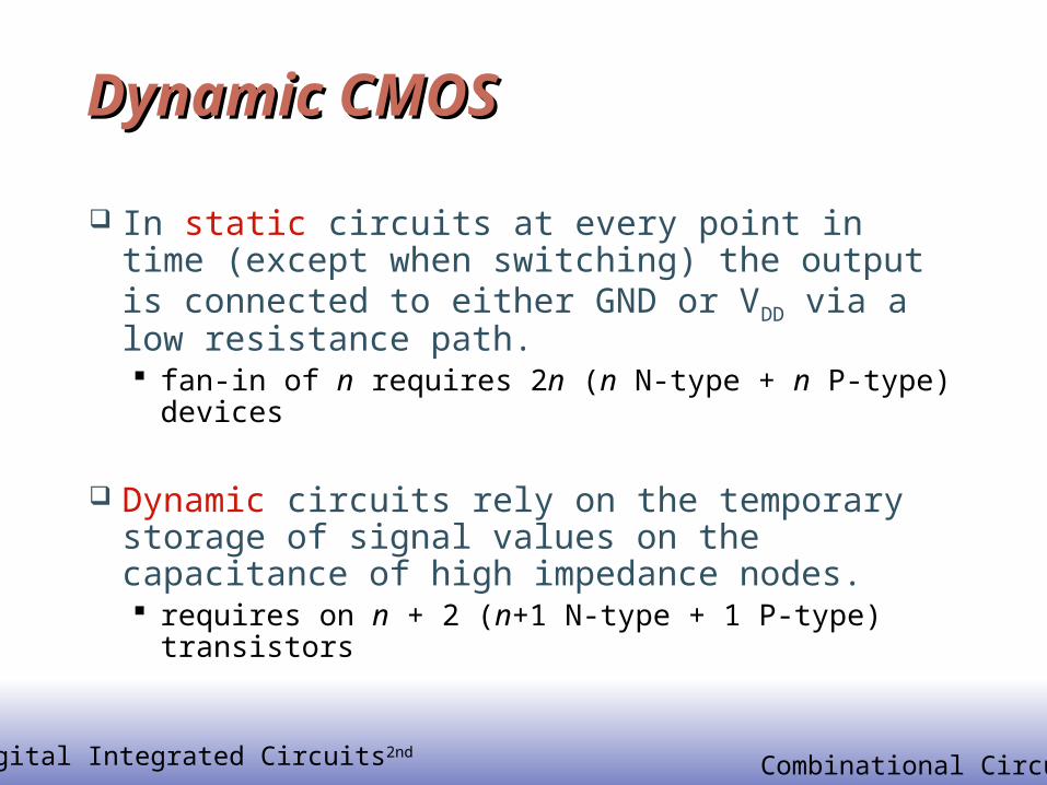
Dynamic CMOSDynamic CMOS
In static circuits at every point in time (except when switching) the output is connected to either GND or VDD via a low resistance path. fan-in of n requires 2n (n N-type + n P-type) devices
Dynamic circuits rely on the temporary storage of signal values on the capacitance of high impedance nodes. requires on n + 2 (n+1 N-type + 1 P-type) transistors

EE14129
© Digital Integrated Circuits2ndCombinational Circuits
Dynamic GateDynamic Gate
In1
In2 PDN
In3
Me
Mp
Clk
Clk
Out
CL
Out
Clk
Clk
A
BC
Mp
Me
Two phase operation Precharge (Clk = 0) Evaluate (Clk = 1)
on
off
1
off
on
((AB)+C)

EE14130
© Digital Integrated Circuits2ndCombinational Circuits
Conditions on OutputConditions on Output
Once the output of a dynamic gate is discharged, it cannot be charged again until the next precharge operation.
Inputs to the gate can make at most one transition during evaluation.
Output can be in the high impedance state during and after evaluation (PDN off), state is stored on CL

EE14131
© Digital Integrated Circuits2ndCombinational Circuits
Properties of Dynamic GatesProperties of Dynamic Gates
Logic function is implemented by the PDN only number of transistors is N + 2 (versus 2N for static complementary
CMOS)
Full swing outputs (VOL = GND and VOH = VDD) Non-ratioed - sizing of the devices does not affect
the logic levels Faster switching speeds
reduced load capacitance due to lower input capacitance (Cin)
reduced load capacitance due to smaller output loading (Cout) no Isc, so all the current provided by PDN goes into discharging CL
EE14132
© Digital Integrated Circuits2ndCombinational Circuits
Properties of Dynamic GatesProperties of Dynamic Gates
Overall power dissipation usually higher than static CMOS no static current path ever exists between VDD and GND
(including Psc) no glitching higher transition probabilities extra load on Clk
PDN starts to work as soon as the input signals exceed VTn, so VM, VIH and VIL equal to VTn
low noise margin (NML)
Needs a precharge/evaluate clock

EE14133
© Digital Integrated Circuits2ndCombinational Circuits
Issues in Dynamic Design 1: Issues in Dynamic Design 1: Charge LeakageCharge Leakage
CL
Clk
Clk
Out
A
Mp
Me
Leakage sources
CLK
VOut
Precharge
Evaluate
Dominant component is subthreshold current

EE14134
© Digital Integrated Circuits2ndCombinational Circuits
Solution to Charge LeakageSolution to Charge Leakage
CL
Clk
Clk
Me
Mp
A
B
Out
Mkp
Same approach as level restorer for pass-transistor logic
Keeper
EE14135
© Digital Integrated Circuits2ndCombinational Circuits
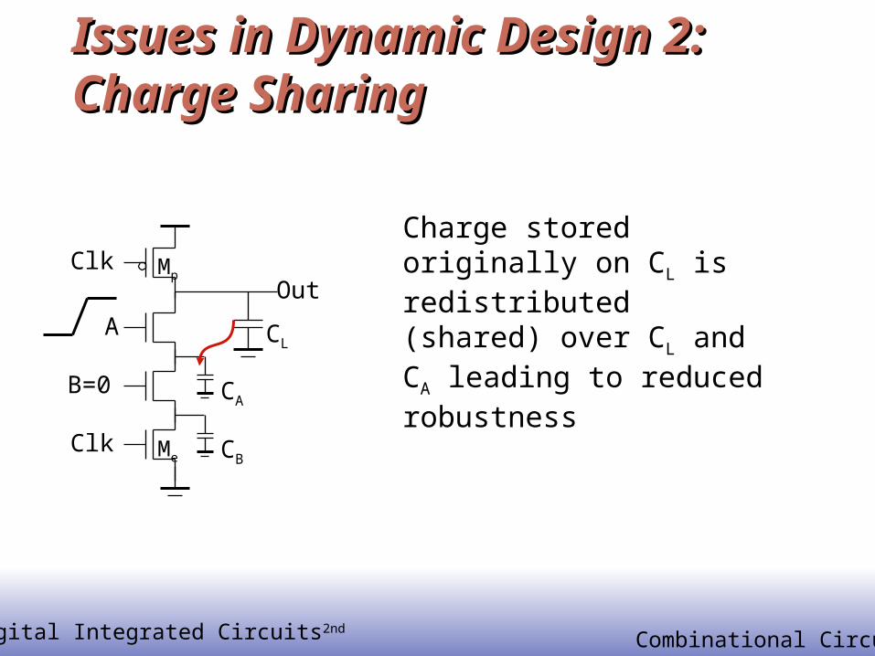
Issues in Dynamic Design 2: Issues in Dynamic Design 2: Charge SharingCharge Sharing
CL
Clk
Clk
CA
CB
B=0
A
OutMp
Me
Charge stored originally on CL is redistributed (shared) over CL and CA leading to reduced robustness

EE14136
© Digital Integrated Circuits2ndCombinational Circuits
Charge Sharing ExampleCharge Sharing Example
CL=50fF
Clk
Clk
A A
B B B !B
CC
Out
Ca=15fF
Cc=15fF
Cb=15fF
Cd=10fF

EE14137
© Digital Integrated Circuits2ndCombinational Circuits
Charge SharingCharge Sharing
Mp
Me
VDD
Out
A
B = 0
CL
Ca
Cb
Ma
Mb
X
CLVDD CLVout t Ca VDD VTn VX – +=
or
Vout Vout t VDD–CaCL-------- VDD VTn VX
– –= =
Vout VDD
CaCa CL+----------------------
–=
case 1) if Vout < VTn
case 2) if Vout > VTnB 0
Clk
X
CL
Ca
Cb
A
Out
Mp
Ma
VDD
Mb
Clk Me

EE14138
© Digital Integrated Circuits2ndCombinational Circuits
Solution to Charge Solution to Charge RedistributionRedistribution
Clk
Clk
Me
Mp
A
B
OutMkp
Clk
Precharge internal nodes using a clock-driven transistor (at the cost of increased area and power)

EE14139
© Digital Integrated Circuits2ndCombinational Circuits
Issues in Dynamic Design 3: Issues in Dynamic Design 3: Backgate CouplingBackgate Coupling
CL1
Clk
Clk
B=0
A=0
Out1Mp
Me
Out2
CL2
In
Dynamic NAND Static NAND
=1=0

EE14140
© Digital Integrated Circuits2ndCombinational Circuits
Backgate Coupling EffectBackgate Coupling Effect
-1
0
1
2
3
0 2 4 6
Vol
tage
Time, ns
Clk
In
Out1
Out2

EE14141
© Digital Integrated Circuits2ndCombinational Circuits
Issues in Dynamic Design 4: Issues in Dynamic Design 4: Clock FeedthroughClock Feedthrough
CL
Clk
Clk
B
A
OutMp
Me
Coupling between Out and Clk input of the precharge device due to the gate to drain capacitance. So voltage of Out can rise above VDD. The fast rising (and falling edges) of the clock couple to Out.

EE14142
© Digital Integrated Circuits2ndCombinational Circuits
Clock FeedthroughClock Feedthrough
-0.5
0.5
1.5
2.5
0 0.5 1
Clk
Clk
In1
In2
In3
In4
Out
In &Clk
Out
Time, ns
Vol
tage
Clock feedthrough
Clock feedthrough

EE14143
© Digital Integrated Circuits2ndCombinational Circuits
Other EffectsOther Effects
Capacitive coupling Substrate coupling Minority charge injection Supply noise (ground bounce)

EE14144
© Digital Integrated Circuits2ndCombinational Circuits
Cascading Dynamic GatesCascading Dynamic Gates
Clk
Clk
Out1
In
Mp
Me
Mp
Me
Clk
Clk
Out2
V
t
Clk
In
Out1
Out2V
VTn
Only 0 1 transitions allowed at inputs!

EE14145
© Digital Integrated Circuits2ndCombinational Circuits
Domino LogicDomino Logic
In1
In2 PDN
In3
Me
Mp
Clk
ClkOut1
In4 PDN
In5
Me
Mp
Clk
ClkOut2
Mkp
1 11 0
0 00 1

EE14146
© Digital Integrated Circuits2ndCombinational Circuits
Why Domino?Why Domino?
Clk
Clk
Ini PDNInj
Ini
Inj
PDN Ini PDNInj
Ini PDNInj
Like falling dominos!

EE14147
© Digital Integrated Circuits2ndCombinational Circuits
Properties of Domino LogicProperties of Domino Logic
Only non-inverting logic can be implemented Very high speed
static inverter can be skewed, only L-H transition Input capacitance reduced – smaller logical effort

EE14148
© Digital Integrated Circuits2ndCombinational Circuits
Designing with Domino LogicDesigning with Domino Logic
Mp
Me
VDD
PDN
Clk
In1
In2
In3
Out1
Clk
Mp
Me
VDD
PDN
Clk
In4
Clk
Out2
Mr
VDD
Inputs = 0during precharge
Can be eliminated!

EE14149
© Digital Integrated Circuits2ndCombinational Circuits
Footless DominoFootless Domino
The first gate in the chain needs a foot switchPrecharge is rippling – short-circuit currentA solution is to delay the clock for each stage
VDD
Clk Mp
Out1
In1
1 0
VDD
Clk Mp
Out2
In2
VDD
Clk Mp
Outn
InnIn3
1 0
0 1 0 1 0 1

EE14150
© Digital Integrated Circuits2ndCombinational Circuits
Differential (Dual Rail) DominoDifferential (Dual Rail) Domino
A
B
Me
Mp
Clk
ClkOut = AB
!A !B
MkpClk
Out = ABMkp Mp
Solves the problem of non-inverting logic
1 0 1 0
onoff

EE14151
© Digital Integrated Circuits2ndCombinational Circuits
np-CMOSnp-CMOS
In1
In2 PDN
In3
Me
Mp
Clk
ClkOut1
In4 PUN
In5
Me
MpClk
Clk
Out2(to PDN)
1 11 0
0 00 1
Only 0 1 transitions allowed at inputs of PDN Only 1 0 transitions allowed at inputs of PUN
EE14152
© Digital Integrated Circuits2ndCombinational Circuits
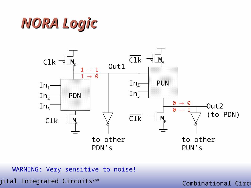
NORA LogicNORA Logic
In1
In2 PDN
In3
Me
Mp
Clk
ClkOut1
In4 PUN
In5
Me
MpClk
Clk
Out2(to PDN)
1 11 0
0 00 1
to otherPDN’s
to otherPUN’s
WARNING: Very sensitive to noise!

EE14153
© Digital Integrated Circuits2ndCombinational Circuits
Homework 6Homework 6
1. Design (in Sue) a CPL version of the 16-bit ripple adder using transistors from the AMI 0.6 process. Simulate in Hspice and measure the worst case delay and average power/MHz.
2. Design (in Sue and simulate) a Domino version of the same ripple adder – measure the w.c. delay and average power/MHz.
(How do these designs compare to Static CMOS?)
Related Documents