ECE 477 Final Report Spring 2010 Team 2 eV-TEK Team Members: #1: _Andrew Phillips___________ Signature: ____________________ Date: _________ #2: _Ben Laskowski____________ Signature: ____________________ Date: _________ #3: _Rob Swanson_____________ Signature: ____________________ Date: _________ #4: _Shannon Abrell___________ Signature: ____________________ Date: _________ CRITERION SCORE MPY PTS Technical content 0 1 2 3 4 5 6 7 8 9 10 3 Design documentation 0 1 2 3 4 5 6 7 8 9 10 3 Technical writing style 0 1 2 3 4 5 6 7 8 9 10 2 Contributions 0 1 2 3 4 5 6 7 8 9 10 1 Editing 0 1 2 3 4 5 6 7 8 9 10 1 Comments: TOTAL Shannon Abrell Ben Laskowski Andrew Phillips Rob Swanson

Welcome message from author
This document is posted to help you gain knowledge. Please leave a comment to let me know what you think about it! Share it to your friends and learn new things together.
Transcript

ECE 477 Final Report Spring 2010
Team 2 eV-TEK
Team Members:
#1: _Andrew Phillips___________ Signature: ____________________ Date: _________
#2: _Ben Laskowski____________ Signature: ____________________ Date: _________
#3: _Rob Swanson_____________ Signature: ____________________ Date: _________
#4: _Shannon Abrell___________ Signature: ____________________ Date: _________
CRITERION SCORE MPY PTS
Technical content 0 1 2 3 4 5 6 7 8 9 10 3
Design documentation 0 1 2 3 4 5 6 7 8 9 10 3
Technical writing style 0 1 2 3 4 5 6 7 8 9 10 2
Contributions 0 1 2 3 4 5 6 7 8 9 10 1
Editing 0 1 2 3 4 5 6 7 8 9 10 1
Comments: TOTAL
Shannon
Abrell
Ben
Laskowski
Andrew
Phillips
Rob
Swanson

ECE 477 Final Report Spring 2010
-ii-
TABLE OF CONTENTS
Abstract 1
1.0 Project Overview and Block Diagram 1
2.0 Team Success Criteria and Fulfillment 2
3.0 Constraint Analysis and Component Selection 3
4.0 Patent Liability Analysis 8
5.0 Reliability and Safety Analysis 12
6.0 Ethical and Environmental Impact Analysis 20
7.0 Packaging Design Considerations 24
8.0 Schematic Design Considerations 29
9.0 PCB Layout Design Considerations 33
10.0 Software Design Considerations 39
11.0 Version 2 Changes 47
12.0 Summary and Conclusions 48
13.0 References 48
Appendix A: Individual Contributions A-1
Appendix B: Packaging B-1
Appendix C: Schematic C-1
Appendix D: PCB Layout Top and Bottom Copper D-1
Appendix E: Parts List Spreadsheet E-1
Appendix F: FMECA Worksheet F-1

ECE 477 Final Report Spring 2010
-1-
Abstract
Project eV-TEK, or Telemetry for Electric Karts, is designed to be an aid for Purdue
University‟s Electric Vehicle Grand Prix, a new event to be held each spring. The product
provides the race crew with a means to collect data pertaining to the driver‟s race-day
performance, monitor basic parameters in real-time, and perform detailed analysis on logged data
once the race is complete. The project consists of two main modules, battery monitors and a
main processing unit. The battery monitors are intended to be permanently tied to the large
lithium-iron-phosphate battery packs used by the kart, and the main controller board is charged
with the task of collecting, logging, displaying, and transmitting all required parameters.
1.0 Project Overview and Block Diagram
Project eV-TEK is an electric go-kart monitoring and telemetry system. It is capable
of measuring and reporting individual cell voltages and overall battery pack currents, kart speed
and location, lap count, and an estimate of remaining battery runtime in terms of laps. The
acquired data is stored on an onboard non-volatile memory, transmitted to the pit station, and
presented to the driver, all at the same time. The project was commissioned by the Industrial
Engineering eV Kart Team, who funded its development and provided guidelines on what
functionality the project should contain, based on their experiences with the inaugural eV Grand
Prix, held in April 2010. Figure 1-1 shows a block diagram of the overall system that our senior
design team designed to meet their needs.

ECE 477 Final Report Spring 2010
-2-
Figure 1-1: System block diagram
2.0 Team Success Criteria and Fulfillment
The original eV-TEK project Project-Specific Success Criteria (PSSCs) are as follows:
1. An ability to report the approximate number of laps remaining on a given
battery charge
2. An ability to detect and report cell voltage anomalies
3. An ability to sense and display kart speed
4. An ability to track the number of laps completed
5. An ability to log and display vehicle telemetry data

ECE 477 Final Report Spring 2010
-3-
The team believes that each of these criteria has been fully met. The final project
reports the estimated number of laps remaining in two forms. The driver is presented with a
digital readout that updates after the completion of each lap during the race, and the pit station is
presented with a readout that updates as new telemetry is received (approximately five times per
second). Thorough testing suggests that these displays are correct based on calculations
performed using data reported from the telemetry system. Furthermore, a percentage state-of-
charge reading is computed for each battery pack and is reported to both the pit station and driver
via digital and analog readouts, respectively.
The project similarly achieved an ability to detect and report cell voltage anomalies.
Each time the battery monitors output a new data point (approximately ten times per second),
each cell voltage is compared to high and low voltage thresholds defined in the main code. If
any cell exceeds either of these limits for a settable number of sample periods, the cell is flagged
as “bad” and is reported to the driver. The time delay is built in due to the voltage fluctuations
expected during normal operation of the kart; hard acceleration creates a voltage drop across the
battery packs due to a large instantaneous current draw.
Next, the project successfully achieved an ability to sense and display kart speed. The
speed is sensed via a pulse-per-revolution created on the main drive shaft of the kart.
Fourth, a lap counter was successfully implemented. The lap counter is based on GPS,
which affords the race team the additional capacity to see current draw, motor voltage, and speed
based on position in the logged data file. The lap counter worked flawlessly each time it was
tested.
Finally, the ability to log and display telemetry data was reached. Five times per
second, the firmware writes all measured and derived kart parameters to onboard non-volatile
memory. This same data is also transmitted to the pit station and presented in an easy-to-use
format for race day kart monitoring. Finally, a log viewer application was developed that reads
the entire onboard memory and creates a comma-separated value (CSV) file for later analysis.
3.0 Constraint Analysis and Component Selection
3.1 Introduction
This project involves creating a data acquisition and telemetry system for electric go-
karts. This system focuses on monitoring kart data and status in order to provide the team, driver

ECE 477 Final Report Spring 2010
-4-
and pit, with the appropriate information needed to enhance their race performance and give
them a higher likelihood of winning the race. Since this system is integrated on a battery-
powered kart, power consumption is of great concern. The design needs to minimize the current
draw of the system so that it does not drain large amounts of power out of the batteries. Another
design issue is the need to monitor large voltages and currents from the main battery packs.
Appropriate isolation of our system from these large values will need to be implemented. Finally,
due to time constraints, commercial part availability is of the utmost importance.
3.2 Design Constraint Analysis
This project is subject to a number of different design constraints. The most important
of these are on-chip peripherals, cost, and power usage. Due to the large number of components
being interfaced to the main controller, it is necessary for the main microcontroller to contain all
of the on-chip peripherals needed. This includes five serial channels, three ADC channels, SPI,
analog inputs, a pulse accumulator and four PWMs. The next major constraint is cost. Though
the customer has promised priority funding, it is desired to minimize cost to the extent possible.
This will provide the customer with greater value while ensuring that the project goals are met on
time. The final major constraint is power consumption. This product will be run on battery
power. Therefore, choosing components which minimize power consumption will be ideal.
3.2.1 Computation Requirements
The most noteworthy item with regard to computational requirements is the main
microcontroller clock frequency. A minimum clock frequency of 20MHz is chosen because it is
easy to implement. Also, this frequency is high enough to ensure that all processes have enough
time to be carried out correctly.
3.2.2 Interface Requirements
General purpose interface requirements for the main controller will consist of 5 pins
for status monitoring inputs and 8 pins for external driver indicators. The input pins will receive
signals from various switches and buttons located on the kart which are provided by the
customer. These will include power switches and enable/disable buttons. The output pins drive
multi-color LEDs which will glow green if a system is active, yellow if connection is lost, and

ECE 477 Final Report Spring 2010
-5-
red if an error occurs. These pins must be able to source 15 to 20 mA of current for driving the
displays.
3.2.3 On-Chip Peripheral Requirements
The main controller will require a wide array of on-chip peripherals. Five serial
connections will be needed to provide communication between the main controller and other
product components including two battery monitors, wireless communication module, GPS
module, and a computer. An SPI will be needed for on-kart data logging. Analog inputs will be
needed for monitoring motor temperature, pedal position, and other future customer needs.
Digital inputs will be used to interface with the speed sensor. Two PWM outputs will be used to
drive motor servos which serve as dial displays to the driver.
The battery monitoring controllers will have a separate set of requirements. Each chip
needs to contain 13 ADCs in order to monitor 12 cell voltages and one pack current with a
resolution of 12 bits. Also, they must contain an external reference pin for a voltage reference
and a UART channel for communicating with the main controller.
3.2.4 Off-Chip Peripheral Requirements
There are relatively few off chip peripherals that will be required for this project.
Voltage followers will be used to isolate battery cell voltages from the battery monitor
microcontroller. A 2MB non-volatile memory chip will be connected to the main microcontroller
to allow for data logging at a speed of 10MHz. Finally, a 900MHz XBee Pro wireless module
will transmit data from the kart to a receiving computer station located in the pit area.
3.2.5 Power Constraints
This product will be implemented on a battery powered electric go-kart. Each of the
two battery packs for the kart consists of 12 individual cells, each with a voltage of 3.3V. System
power consumption should be minimized as much as possible, however, it is understood that any
power used by this system will be relatively minute compared to the power consumed by the
motor. For this reason it was decided that the battery monitor systems would be powered off of
the two lowest cells from a given pack. These monitors will only draw approximately 15mA at
5V. The main control board and its attached peripherals combined will draw approximately 2A

ECE 477 Final Report Spring 2010
-6-
at a maximum of 12V. Due to this large current draw during full operation, it was decided that an
externally provided 12V minimum 3Ah battery will be needed to supply the system for the
duration of the race.
3.2.6 Packaging Constraints
As this product is being implemented on a go-kart, the product is not necessarily
constrained by size. There will be ample room on-kart for the product to fit without interfering
with other kart components. However, it is desired that the main product components be
contained within a single plastic enclosure approximately 9x6x3.5 in. This enclosure will contain
the main board, wireless module, GPS module, and all driver displays. All other components,
including the battery monitor and various sensors, will connect to this central enclosure via a
self-contained wiring harness. Ideally, this enclosure will be able to protect the main components
from outside elements as well as be secure enough to handle kart vibration.
3.2.7 Cost Constraints
As this product is being developed for the IE EVGP team, the customer has agreed to
take responsibility for all project costs. A recent meeting with the customer resulted in the
agreement that this project is the top priority for their team. Therefore, it is believed that cost is
not a limiting factor for this project. That said, this does not constitute a “blank check.” All
possible cost saving choices will be taken into consideration in an attempt to keep the project
cost under $1000.
3.3 Component Selection Rationale
The first component needed is the differential amplifier that will be used in the battery
management system. The first part considered is a TI INA148. This is a +/-200V common-mode
voltage difference amplifier. This amplifier is precise (max gain error of .075%), low-power
(quiescent current of 260µA), and has unity gain [1]. The INA148 comes in a small SO-8
surface-mount package [1]. The price per unit of this part is $6.25 [2]. The second part being
considered is the LM324. This part lacks the precision of the INA148 and has slightly fewer
features. The accuracy of the LM324 can be increased by the choice of an external precision
resistor network. This addition allows the LM324 to achieve results similar to the INA148 at a

ECE 477 Final Report Spring 2010
-7-
significantly lower cost. The LM324 sells for a per-unit price of $0.50 for a quad pack [3].
Considering the large quantity of parts needed for this application, choosing the less expensive
option will prove to be a wise decision. Additionally, using the quad pack will decrease the space
required for construction of the product.
The next component to be identified is the microcontroller in charge of the battery
management system. This component will monitor numerous cell voltages through the
differential amplifiers, measure the current entering or leaving the entire battery pack, calculate
the total charge in the pack, and relay that information back to the main controller. There are two
candidate parts that could fit this application. The first is a PIC18F46K20. This part contains 13
ADC channels with 10 bits of resolution per channel, a UART, has a clock frequency of 64MHz,
and runs off of a nominal 3.3V supply voltage [4]. The second candidate is the PIC18F4423.
This part has 13 ADC channels with 12 bits of resolution per channel, a UART, a maximum
clock frequency of 40MHz, and can run off of a 5V supply [5]. After comparing the two parts,
the PIC18F4423 was chosen due to its increased resolution. The decrease in clock speed will not
affect the end product due to the non-time critical nature of the application.
The final component to be identified is the main microcontroller. The first candidate
part is the PIC32MX575F256L. This part has six UARTs, five PWM channels, sufficient ADC
channels, runs at a clock speed of 80MHz, contains 85 I/O pins with high source and sink
capability, and runs off of 3.3V [6]. These criteria make this part a sufficient choice for the main
controller. The second candidate is the LPC1756. This part has comparable features to the PIC
and comes in a larger package; however, it only has 52 I/O pins [7]. Ultimately, due to the design
team‟s previous experience with the PIC line of microcontrollers, the PIC32MX575F256L has
been chosen as the main controller for the project.
3.4 Summary
This report is an overview of the design constraints that must be considered for the selection of
the main components for the eV-TEK product. The computation, interface, on and off-chip
peripheral, power, packaging, and cost constraints have been examined. To that end, appropriate
major components have been identified that will meet the stated constraints. Finally, Appendix E
contains a parts listing.

ECE 477 Final Report Spring 2010
-8-
4.0 Patent Liability Analysis
4.1 Introduction
Project eV-TEK is a data acquisition and telemetry system intended for use on electric
go-karts. This system focuses on monitoring kart data and status in order to provide the driver
and pit with the appropriate information needed to enhance their race performance and give them
a higher likely hood of winning the race. This information includes speed, a lap counter, and
battery status, which is a measurement of how much charge is left within the battery packs on the
kart. All of these criteria are logged on the kart itself as well as transmitted wirelessly to the pit
crew.
With electric vehicles in general being a newer technology to the public, patent liability with
projects of this nature did not present too much of an issue. A few of the patents found included
an electric vehicle monitoring system, a battery monitor for electric vehicles, and a monitoring
apparatus and method for battery power supply. While this report highlights the patents found
regarding electric vehicles in general, there is a group of patents that involve race telemetry
systems that should be considered before further production of this project.
4.2 Results of Patent and Product Search
An Electric Vehicle Monitoring System, US Patent 5534759, a Battery Monitor for Electric
Vehicles, US Patent 5646534, and a Monitoring Apparatus and Method for Battery Power
Supply, US Patent 4390841, are some of the best matches found that perform substantially the
same function as this project. Patent 759 performs similar functions to that of eV-TEK. Both
patent 534 and 841 are just a part of what eV-TEK is capable of performing.
The Electric Vehicle Monitoring System, patent 5534759, was filed on May 19th
of 1995.
Abstract: “This system is used for measuring electric vehicle performance. This system
includes sensors for obtaining vehicle performance data and operating parameters; a
digital dashboard with information on the vehicle's operating parameters; a data
acquisition system for collecting the data from the sensors and converting it into a digital
format; and a removable computer for storing, evaluating and providing reports of the
data. It was specifically designed for use in an electric propulsion vehicle or an internal
combustion engine vehicle converted to electric power.” [8]

ECE 477 Final Report Spring 2010
-9-
The first claim of this patent, which is an overview of the entire product, is the most
pertinent when it comes to infringement. The possibilities for infringement lie within the
statements;
Claim 1: “A data acquisition means electrically connected to said sensor means for
collecting said data signals from said sensor means and converting said data signals from
said sensor means into digital input signals; a processing unit electrically connected to
said data acquisition means for receiving said digital input signals from said data
acquisition means, said processing unit storing and interpreting said digital input signals,
said processing unit further generating reports of said performance characteristics; and an
operator display electrically connected to said sensor means for displaying operating
characteristics of said electric powered vehicle, said operating characteristics
corresponding to at least one of said performance characteristics, said operator display
located within said electric powered vehicle to be in view of an operator of said vehicle
when said operator is driving said vehicle.” [8].
With further inspection of the rest of the claims in this patent, it is apparent that the infringement
only exists under the doctrine of equivalents.
The Battery Monitor for Electric Vehicles, patent 5646534, was filed on January 6th
in
1995. This system monitors the voltage and temperature of the batteries associated with a
battery pack of an electric vehicle. It utilizes optical isolators to monitor the battery voltage of
each individual battery. The monitor itself is located in a position close to the battery pack. The
monitor then sends the collected data back to a vehicle controller. This patent is an example of
literal infringement by eV-TEK. A few key examples of claims where infringement occurs are
claims 1, 7, and 9.
Claim 1: “…means for providing battery voltage signals indicative of the battery
voltage of each of the plurality of batteries.”[9]
Claim 7: “…the battery monitor monitors the batteries associated with an electric
vehicle, said battery monitor being positioned proximate to a battery tub that
holds the plurality of batteries.”[9]
Claim 9: “…means for providing battery voltage signals indicative of the battery
voltage of each of the plurality of batteries; selecting means for selecting one of
the battery voltage signals from the plurality of batteries” [9].
The Monitoring Apparatus and Method for Battery Power Supply, patent 4390841,
was filed on October 10, 1980.
Abstract: “This is used for monitoring and/or indicating energy that a battery power
source has remaining and/or can deliver for utilization purposes as, for example, to an
electric vehicle. A mathematical model forms the basis for monitoring by predicting the
remaining battery life from the discharge current rate and the battery parameters.

ECE 477 Final Report Spring 2010
-10-
Through use of a microprocessor with central information storage of temperature, current
and voltage, system behavior is monitored, and system flexibility is enhanced.” [10].
This patent was filed over 20 years ago, so it is no longer enforceable. It is, however, still
considered prior art.
4.3 Analysis of Patent Liability
Literal infringement occurs with patent 534. The battery monitoring system is only
one part of eV-TEK, however the way in which battery monitoring is executed is almost exactly
the same as patent 534. There are only a few notable differences between eV-TEK and patent
534.
One of the main differences between eV-TEK and patent 534 is the use of optical
isolators. Due to a lack of a common ground between the main board and battery monitors, eV-
TEK utilizes optical isolators on the serial data link between the two boards. Patent 534 uses
optical isolators to reference the voltages of the individual cells, therefore application of the
optical isolators is significantly different. According to claim 4 of patent 534;
“…the isolator means is a plurality of opto-isolators, wherein an opto-isolator is provided
for each battery being monitored, and wherein a particular opto-isolator charges a
capacitor when the particular opto-isolator is selected to determine a particular battery
voltage.” [9].
Also according to claim 5,
“…the isolator means is an opto-isolator, said opto-isolator isolating the battery voltage
of each of the plurality of batteries from the controller means.” [9].
Another difference between the two systems is that eV-TEK does not measure the temperature of
the batteries, whereas the battery monitor for electric vehicles does.
Patent 759 was a second patent found dealing with electric vehicles that eV-TEK infringes
upon under the doctrine of equivalents. In regards to patent 759, the first claim on the patent
seems to be a very close literal infringement. However, with closer inspection of the other claims
in the patent, it is found that eV-TEK uses a different method to complete similar tasks.
Patent 759 measures the voltage across the main power source.
Claim 2: “A system according to claim 1 wherein said first voltmeter is a differential
voltmeter, said first voltmeter being further isolated from an electrical grounding system of
said electric powered vehicle, said ground isolation allowing said first voltmeter to measure
main voltage without discharging said main electric power source” [8].

ECE 477 Final Report Spring 2010
-11-
The eV-TEK system measures the individual cells in the main power supply and brings
them together to analyze the remaining overall voltage. Patent 759 uses a shaft encoder to
measure the speed of the vehicle.
Claim 5: “A system according to claim 1 wherein said plurality of optical shaft encoders
further comprises: a first shaft encoder for providing measurements corresponding to a
speed of said electric powered vehicle…” [8].
An inductive proximity sensor is used by eV-TEK to measure the speed of the kart. Another
difference between the two systems is the fact that patent 759 uses an onboard portable computer
that interfaces with the vehicle;
Claim 6: “…said processing unit is a portable computer having a processing power
source separate from said main electric power source and separate from said accessory
electric power source; said portable computer further comprises a memory for storing
additional data input into said memory by an operator of said electric powered vehicle;
said processing unit senses the position of an ignition switch of said electric powered
vehicle; said processing unit enters a standby mode when said ignition switch is in an off
position, said standby mode conserving said processing power source; and said
processing unit enters an active mode when said ignition switch is in an on position, said
active mode storing and interpreting said digital input signals from said data acquisition
means” [8].
The eV-TEK system communicates the data wirelessly as well as logging the data to the onboard
microcontroller to be viewed at a later time. Patent 759 utilizes a general purpose laptop
computer that is controlled by the vehicle to log the data.
4.4 Action Recommended
During the research of patents, eV-TEK literally infringes upon patent 534. With
further inspection of this patent, eV-TEK‟s battery monitoring system is executed in exactly the
same way as the product described in this patent. A way to not infringe upon this patent is to
completely reconstruct eV-TEK‟s battery monitoring system. One way of achieving this would
be to use separate ADCs on each individual battery cell which have a serial data output. These
would output at a continuous data bit stream. The bit streams from every ADC will then be
concatenated by an FPGA. Once concatenated the serial bit stream will be transmitted by an
optical isolator to the main board.
4.5 Summary

ECE 477 Final Report Spring 2010
-12-
Electric vehicles are one of the newer technologies on the market. Since they are such
a new technology, there were only a few patents that dealt with electric vehicle monitoring.
Since eV-TEK is built for a kart racing situation, there is also a whole different realm of products
which deal with racing telemetry and should be examined. The ones found for this report were
analyzed and compared with eV-TEK. Patent 534, which was found to deal with battery
monitoring on an electric vehicle, was found to be a literal infringement on the part of eV-TEK.
The other two patents found, patent 759 and patent 841 were just infringed upon under the
doctrine of equivalents. With prior research of patents before the initial brainstorming of eV-
TEK, infringement could have been avoided.
5.0 Reliability and Safety Analysis
5.1 Introduction
Team eV-TEK aims to produce a telemetry system for electric go-karts specifically
targeted at Purdue University‟s annual Electric Vehicle Grand Prix race. The telemetry system
has several important monitoring tasks that must be completed reliably and safely. As the kart
will operate off of a very large lithium-iron-phosphate battery pack, careful monitoring of charge
state is vital to promote safety of the driver, of the batteries, and of bystanders. The telemetry
system must also monitor important vehicle characteristics such as motor temperature and
overall current draw and report any anomalies to the driver and pit crew. While the system is not
so deeply integrated into the kart as to have a telemetry malfunction affect safe go-kart operation,
it is certainly desirable to make the system reliable as possible as well.
In the final design, the team believes that the components responsible for most
potential reliability issues will be both the main board and battery board microcontrollers, both
main board voltage regulators, and the current sense resistor. These components represent the
ones that are the most complex and those that operate at elevated temperatures, respectively.
This report will also examine several possible failure modes for each functional block of the
system, the effects of each failure, and the seriousness of each failure with regard to safety.
5.2 Reliability Analysis

ECE 477 Final Report Spring 2010
-13-
The components selected for the reliability analysis are the battery monitoring
microcontroller, the battery pack current sense resistor, the main board microcontroller, and both
voltage regulators on the main board. For clarity, the reliability analysis is separated into sub-
sections for each component with above-average risk of failure. All reliability data is taken from
manufacturer data sheets where information is available; otherwise, information is sourced from
the MIL-HDBK-217F specification [11]. The model used for each microcontroller was the
Digital Microprocessor model; for each voltage regulator, the Linear Microcircuit model; and for
the resistor, the Wirewound Fixed Power Resistor model.
5.2.1 Battery Monitor Microcontroller
Due to its high complexity relative to the other components on the battery monitoring circuit
boards, the battery monitoring microcontroller, a PIC18F4423, was selected for inclusion in the
reliability analysis. It operates well within the range approved by its manufacturer, Microchip
Technology, so it is assumed that probability of failure in practice will be quite low.
Nevertheless, it is by far the most complex component on the battery board. Table 5-1 presents
the values and assumptions used to estimate its Mean Time to Failure (MTTF). Note that the
value for parameter πT was chosen based on operation at a 25 degree Celsius case temperature, a
junction-to-case thermal resistance of 22 ˚C/W (found in [11]), and a power dissipation of 0.1W,
calculated according to the method in [5]. This power dissipation assumes the microcontroller
core operates at 10MHz and that one I/O pin is active, sourcing 10mA. This assumption is valid
for our application because only one microcontroller pin actively sources appreciable current.
Parameter name Description
Value Comments
C1 Die complexity 0.14 8-bit MOS microprocessor
πT Temperature coefficient 0.095 See text
C2 Package failure rate 0.019 40 functional pins
πE Environment factor 4.0 Ground mobile
πQ Quality factor 10 Commercial product
πL Learning factor 1.0 4 years in production
Battery
microcontroller:
λp = (C1πT + C2πE)πQπL 0.893 Failures per 106 hours
( ~ 128 years)
Table 5-1: Predicted failure rate for PIC18F4423

ECE 477 Final Report Spring 2010
-14-
5.2.2 Current Sense Resistor
The current sense resistor is included in the reliability analysis due to the expectation that it
will operate at an elevated temperature. Since the full current consumed by the go-kart‟s motor
must pass through this resistor, it is expected that its required power dissipation will be quite
high compared to the remainder of the system components. A resistor with a 100-Watt
continuous power rating was chosen; however, brief excursions to a 500-Watt dissipation level
are acceptable [12]. Table 5-2 presents predicted failure information for the current sense
resistor.
Parameter name Description
Value Comments
λb Base failure rate 0.0357
1.0 stress factor, 25 ˚C
ambient
πR Resistance factor 1.0 RW type, up to 100 ohm
πE Environment factor 8.0 Ground mobile
πQ Quality factor 15 “Lower quality” [11]
Current sense
resistor:
λp = λbπRπQπE 4.284 Failures per 106 hours
( ~ 27 years)
Table 5-2: Predicted failure rate for current sense resistor
5.2.3 Main Board Microcontroller
The PIC32MX575F256L microcontroller found on the main controller board is the most
complex component in the entire project, at least on the basis of transistor count, thus it is
included in the reliability analysis. See Table 5-3 for the PIC32 reliability computations. The
value for parameter πT was computed assuming a 25 degree Celsius case temperature, a junction-
to-ambient thermal resistance of 43 ˚C/W [13], a power dissipation of 0.5 Watts, and a junction
temperature of 46.5 degrees Celsius. These figures assume that the core is running at 25Mhz and
that 12 I/O lines are each sourcing 10mA; this figure for current draw accounts for the six bi-
color indicator LEDs on the main board. The values supplied in the table are indicative of
conditions slightly worse than what will actually be encountered during normal operation; we
used the next higher category for pin count and the next higher bracket for die temperature.
Parameter name Description
Value Comments
C1 Die complexity 0.56 32-bit CMOS

ECE 477 Final Report Spring 2010
-15-
microprocessor
πT Temperature coefficient 0.29 See text
C2 Package failure rate 0.068 See text
πE Environment factor 4.0 Ground mobile
πQ Quality factor 10 Commercial product
πL Learning factor 1.5 ~1 year in production
Main
microcontroller:
λp = (C1πT + C2πE)πQπL 6.516 Failures per 106 hours
( ~ 18 years)
Table 5-3: Reliability calculations for main microcontroller
5.2.4 3.3 Volt Regulator
It is expected that the MCP1826S 3.3 Volt regulator on the main control board will operate
at an elevated temperature during normal telemetry system operation, so it is included in the
reliability analysis. This is a linear regulator which dissipates an estimated 1.7 Watts under
normal operation. Table 5-4 details the reliability calculations for this component. For the
temperature computation, an ambient temperature of 25 degrees Celsius was specified along with
a junction-to-case thermal resistance of 3.0 ˚C/W [14] and a case-to-PCB-to-ambient thermal
resistance of 22 ˚C/W [15]. This figure used from [15] is based 5000 mm2 of copper connected
to the thermal tab of the regulator; our PCB has in excess to 8000 mm2 of copper connected to
this tab. The smaller figure is used due to the voids in our copper plane where some traces pass
through it. In reality, the thermal resistance is probably slightly lower than our assumptions.
These figures combine to give an estimated junction temperature of 67.5 degrees Celsius.
Parameter name Description
Value Comments
C1 Die complexity 0.01 1 to 100 transistors assumed
πT Temperature coefficient 1.4 70 ˚C, See text
C2 Package failure rate 0.0012 Three pins
πE Environment factor 4.0 Ground mobile
πQ Quality factor 10 Commercial product
πL Learning factor 1.0 3 years
3.3V regulator: λp = (C1πT + C2πE)πQπL 0.188 Failures per 106 hours
( ~ 607 years)
Table 5-4: Reliability calculations for 3.3V regulator
5.2.5 5 Volt Regulator

ECE 477 Final Report Spring 2010
-16-
Similarly, the TPS5420 5 Volt regulator on the main control board is included in the analysis
due to the likelihood of operation at elevated temperatures. As nearly all power for the main
control board (except for the power used to operate the speed sensor) flows through this
regulator, its continued reliable operation is of the utmost importance. Parameters used for the
5V regulator reliability calculation can be found in Table 5-5. For the value of πT, the method
for computing power dissipation found in [16] was used to arrive at an estimated dissipation of
0.54 Watt. With a junction-to-ambient thermal resistance using the values from [16] and the data
from [15], the estimated junction temperature is 65.5 degrees Celsius.
Parameter name Description
Value Comments
C1 Die complexity 0.01 Based on 1-100 transistors
πT Temperature coefficient 2.0 See text
C2 Package failure rate 0.0034 8-pin SOIC
πE Environment factor 4.0 Ground mobile
πQ Quality factor 10 Commercial product
πL Learning factor 1.0 4 years
5V regulator: λp = (C1πT + C2πE)πQπL 0.336 Failures per 106 hours
( ~ 340 years)
Table 5-5: Reliability information for TPS5420
5.2.6 Conclusions
Based on the components selected for analysis, believed to be the ones most likely to
fail, it is expected that the telemetry system presented herein will experience approximately
12.217 failures per 106 hours, for an overall mean time to failure of approximately 9.3 years. As
over half of those failures can be traced back to the microcontroller on the main control board,
perhaps the best way to improve reliability of the telemetry system would be to change the main
microcontroller for one that is less complex, more mature, or both. If that were not an option,
reducing its power dissipation by decreasing clock frequency or decreasing sourced current
would be a valid strategy for increasing its predicted longevity. The use of external drivers for
the relatively high-current LED drive lines or the use of heatsinks on some of the other
components with high operating temperature could also significantly improve the project‟s
projected time to failure.
5.3 Failure Mode, Effects, and Criticality Analysis (FMECA)

ECE 477 Final Report Spring 2010
-17-
To facilitate analysis of design failure points, both the battery monitoring module and
main controller board were divided into functional groups and the failure mechanisms for each
group analyzed. Criticality for each failure mode is defined as follows:
High: Potential injury to a human
Medium: Potential lasting damage to the telemetry system
Low: No lasting damage (power cycling or reseating a connector could fix the problem)
The battery monitoring power supply is the first block that will be considered. This
block contains a linear voltage regulator, a 4.096-volt precision reference, and a 2.500-volt
precision reference. The main failure modes for this block include the possibility that each
voltage might be too low or too high. Voltages that are below the specified values would most
likely be attributed to a shorted bypass capacitor; this event would likely cause an overcurrent
condition at the affected component (regulator or voltage reference) and damage or destroy the
component. More immediate indications that a voltage reference or regulator has zero output
include consistently inaccurate measurements or an altogether lack of data output from the board.
A damaged or destroyed component, on the other hand, could lead to too high a voltage being
output from the affected part and can cause possible further damage to the battery monitoring
board. As the battery boards are optically isolated from the main board, the damage should not
propagate past the bounds of the battery monitoring subsystem. Based on the potential damage
to hardware, each of these failure modes is assigned a criticality of Medium.
Next considered is the microcontroller functional block on the battery monitoring
boards. This block is responsible for sequencing all analog inputs and digital outputs. Failure
modes for this block include an incorrect voltage on the MCLR line of the microcontroller and
stuck input pins or output pins. The first, an incorrect MCLR voltage, can be brought about by a
defective, missing, or poorly soldered resistor pulling that line to VCC. With this line floating,
microcontroller operation may be unreliable and unpredictable as the microcontroller floats in
and out of reset. The criticality of this failure mode is Low, as it does not cause lasting damage
to hardware and the failures cannot propagate to other subsystems. Similarly, a stuck output pin
is assigned a criticality of Low since the only real effect is improper operation of the circuit. A
stuck input pin, on the other hand, can possibly damage output drivers on the same PCB that

ECE 477 Final Report Spring 2010
-18-
connect to that input pin and so are assigned a criticality of Medium. Stuck input and output
lines can be attributed to ESD damage or, perhaps more likely, software failure.
The voltage follower circuit from the battery monitoring boards constitutes the next
functional group. Failure modes for this block are centered primarily on unexpected voltages at
the operational amplifier input pins. If the voltage at the input is too low, perhaps caused by a
missing, defective, or poorly soldered R45, the subsystem will report incorrect voltages to the
main board. This failure is assigned a criticality of Low. If, on the other hand, the voltage at the
input is too high (perhaps caused by a missing, defective, or poorly soldered R47), there is a
potential of permanent damage to the op-amp IC. This failure mode is assigned a criticality of
Medium based on this possible effect. Either of these failure modes has the potential to report
incorrect data to the main board.
Next, we move to the main board; specifically, its power supply. The failure modes
here are centered again on either voltage rail being at either too high or too low a voltage.
Voltages on the 5-volt rail that are too high might be attributed to a failed R1 or a defective 5V
regulator; voltages on this rail that are too low are likely due to a shorted bypass or bulk
capacitor, a failed R2, or, again, a general component failure. On the 3V rail, voltages that are
too high are most likely caused by a defective regulator; undervoltages are likely caused by
shorted bypass or bulk capacitors or general component failures. As either regulator can
overheat when shorted, these failures are assigned a criticality of Medium for their potential to
cause lasting hardware damage.
The main microcontroller can fail in much the same way as the battery monitoring
microcontroller; the general microcontroller failure modes common to both will not be repeated
for the sake of brevity. An additional failure mode of the main microcontroller comes in the
form of its analog power supply filter. If this filter fails, it is possible that inaccurate motor
temperature readings will be reported. This in and of itself will not cause lasting hardware
damage and is therefore assigned a criticality of Low.
Next to be considered is the optoisolator block. If any of these ICs were to fail such
that a short existed between the input and output, the telemetry system would likely immediately
cease to function and permanent hardware damage would ensue. This failure mode is detectable
by noticing the plume of smoke from the main board components, and as such, is assigned a
criticality of Medium. A second failure mode of this block is an overcurrent condition on the

ECE 477 Final Report Spring 2010
-19-
emitter portion of the isolators. This failure mode, brought about by a current-limiting resistor
failing shorted, can lead to permanent isolator damage and possible damage to the output driver
driving the isolator. This failure mode is detectable by a permanent cessation of functionality
involving the optoisolators (speed and voltage sensing, servo motor actuation, and battery
information reporting) and is assigned a criticality of Medium. Finally, voltages on the
optoisolators output pins can become stuck high. This failure is brought about by the 1k pullup
resistors on the optoisolators outputs failing shorted. This failure mode is detected by noticing
that no input functions work properly and is assigned a criticality of Medium due to the
possibility of permanent optoisolator damage. A stuck-at-low fault on the optoisolator output is
far less likely since the input would have to become stuck to effect this failure; this falls under
the umbrella of microcontroller output stuck-at faults, discussed previously.
The final major functional block of the main board is the USB to serial converter IC.
Any failure of this component can create an inability to communicate with the PC, introducing
difficulty when the end user attempts to configure the board or read logs from it. The output pin
from this IC can develop a stuck-at fault, making communication impossible. Similarly,
communication becomes impossible if either one of the resistors in its reset circuit fails. Either
of these faults can be observed by a lack of ability to communicate with the main board via this
serial connection. Neither fault creates a possibility of harm to the user or permanent hardware
damage, so all faults with this block are assigned a criticality of Low.
5.4 Summary
This report summarized the expected safety and reliability issues foreseen during the
development of eV-TEK. Components deemed most likely to fail were identified, and failure
rates for each individual component were predicted based on models published by the United
States Military. Solutions were proposed to improve reliability of those components most likely
to fail in a short period of time. Criticality levels for each failure were defined, and it was
determined that eV-TEK should not present a threat of harm to a human under any possible
failure mode.
6 Ethical and Environmental Impact Analysis

ECE 477 Final Report Spring 2010
-20-
6.1 Introduction
The eV-TEK product is an advanced telemetry system designed specifically for
electric powered go-karts. The system is designed to give the operator feedback about kart
parameters, such as speed, battery voltage, system current, and lap count. With very large
lithium-iron-phosphate battery packs, it is very important from an ethical perspective to have
proper voltage and current monitoring of the packs. Our project would suffer a severe breach of
ethics if no effort was made to warn the operators about the dangers of lithium batteries,
especially in large quantities. In addition, the eV-TEK project introduces significant physical
safety concerns to an unsuspecting operator that must be noted to take proper ethical
responsibility. As with any commercial product, eV-TEK also impacts the environment. While
some parts of the project have inevitable environmental impacts, such as manufacturing and
component usage, there are also environmental impacts such as the auxiliary battery which
would harm the environment if not properly handled. It is the sole responsibility of the eV-TEK
organization to make the end user aware of these safety and environmental concerns.
6.2 Ethical Impact Analysis
When releasing any product for consumer use, it is important to hold a high standard
of ethical responsibility in the product. When reviewing the eV-TEK system, some components
can be identified as critical for operator safety, such as the speed sense mechanism and the
battery packs. The method of speed sense employed in the prototype kart involves a stainless
steel bar attached to the main drive shaft. This bar sticks out from the shaft, rotating at the same
rate as the shaft. The inductive proximity sensor sees this bar passing in front of the sensor face,
and sends a corresponding pulse signal to the main board. This steel bar, however, creates a
significant safety hazard to any nearby objects such as wires, race debris, and fingers. The
possibility of an operator being injured by the speed sense system poses serious ethical concerns
for the eV-TEK project, and precautions must be taken to prevent this from happening. This can
be done by including a safety shield over the area where the bar is spinning to prevent accidental
intrusion. Warning labels would also be placed on or near the safety shield to make the operators
aware of the potential danger. A note would also be included in the operations manual making
people aware of the potential risk for injury. Modifications could be made on future system

ECE 477 Final Report Spring 2010
-21-
revisions to replace this bar with a metal disk. The metal disk would have a hole in it large
enough to allow the sensor to toggle between presence and no presence. The key factor about
this disk is that it would remain uniformly round, so that miscellaneous objects cannot be easily
caught in it. They would instead just brush against it. This would significantly reduce the
possibility of personal injury via this safety hazard.
An additional major safety concern is the battery packs on the kart. The development
kart utilizes lithium-iron-phosphate batteries, which as with all lithium derivatives can have
serious detrimental effects if not properly maintained. A large portion of the motivation for
building the eV-TEK battery monitoring system was to monitor the lithium batteries to prevent
unsafe voltage levels. During a race, the driver will wish to drive as long as possible to gain
track position. If the driver is unaware of the battery state, the batteries could be potentially
drained too low and an undervoltage condition could occur. If this condition was to happen to a
lithium chemistry battery, a significant safety concern will result in the possibility of the cell
catching fire or exploding. The eV-TEK system is designed to make the operator aware of
battery status, and make appropriate alerts to the user if the voltage is dropping to an unsafe
level. A portion of the user‟s manual will be dedicated to educating the operator how to
understand the eV-TEK warning system, and what to do in that situation.
Since the eV-TEK system interfaces with a relatively high DC voltage system, it is
very important that proper preproduction testing is performed to ensure quality. Any lose
connections or debris could potentially cause shorts of the battery cells, which would result in a
potentially catastrophic board or battery failure and potential fire hazard. While the kart may not
see the extreme thermal shock and temperature cycling of a conventional vehicle, it will still
experience many stresses on the track, particularly vibration. The eV-TEK design attempts to
counter the effects of vibration by including such special features as locking interconnects. If all
system connectors are locking, the possibility of connections coming loose and allowing
potential shorts is reduced. Proper extended testing will be needed to completely validate the
integrity of the system as a whole.
6.3 Environmental Impact Analysis
Environmental impact is also an important concern of the eV-TEK project. As with
any project that utilizes a battery as its power source, the primary environmental concern of eV-

ECE 477 Final Report Spring 2010
-22-
TEK is the battery. The eV-TEK system is supplied with a dedicated lead acid battery to power
the main controller board. This lead acid battery is supplied as an easy to use power source that
can be charged with any simple lead acid battery charger, available at most kart or automotive
store. While the battery monitoring system runs off the existing lithium cells on the kart, the
main control board has its own dedicated lead-acid battery. This is to prevent unnecessary
current draw from the main battery packs which is needed to supply current to the motor and
ultimately win the race. By having a dedicated 12V battery, it also eliminates the need for
constructing a power supply to drop the karts approximate 80V nominal battery pack to a useable
12V source. The negative effect of including a lead-acid battery is that over the lifetime of the
kart, the battery will inevitably wear out. At that point, if the user chooses to simply throw the
battery away, an unnecessary and unhealthy addition of lead will be put in the earth‟s landfills.
To be environmentally responsible for the components that come with the eV-TEK system, the
operations manual will remind the operator how environmentally hazardous improper disposal is,
and that they should properly recycle the batteries at their local automotive store or waste
agency. Unfortunately cases may arise where the owner still neglects to heed such warning. For
future eV-TEK development, research will be done into alternative forms of portable energy. If
other battery sources prove acceptable for the eV-TEK system, they can be offered as a
consumer selectable option to suit their price range and existing equipment, such as chargers.
Efforts can also be performed to create a high efficiency step down converter so that the main
controller can be run off the kart batteries without significant current draw.
Factors involved in the manufacturing process also pose environmental concerns to the
eV-TEK project. One basic form of hazard is the inclusion of lead in the manufacturing and
assembly of both components and printed circuit boards. Lead, when improperly recycled, can
be very hazardous to the environment and should be avoided if possible. One method of
avoiding this lead hazard is selecting a fabrication house that runs with RoHS lead free
compliance. This would mean that all manufacturing and assembly of the circuit board would be
made with lead free materials. The eV-TEK team could also then review all components used in
the system to evaluate their compliance for lead free status. When a component is found to be
comprised of lead in any regard, effort could be made to find a similar component as a drop in
lead free replacement.

ECE 477 Final Report Spring 2010
-23-
Aside from manufacturing impacts, the operation of the eV-TEK system can also
interfere with the environment around it. Since the eV-TEK system is equipped with an XBee
wireless communication module, it can emit RF energy at approximately 900MHz. While this
functions as a key feature of our system, it may also cause undesirable effects. The XBee is
designed to only communicate with other modules sharing the same network name. However,
even though the communication is linked between the two modules, the transmission is still
propagated everywhere within the surrounding area. If other devices or systems are nearby
operating on the same 900MHz band, they may pick up the eV-TEK‟s transmissions as
interference, potentially leading to undesirable behavior. It is ethically important to the eV-TEK
project to ensure that our project does not operate outside of any federally mandated rules and
cause excess radiation. Therefore, the eV-TEK system would have to pass the FCC. This
certification will validate that we do not unethically generate any unlawful excess noise
radiation, helping to keep the surrounding environmental areas free of the excess noise.
6.4 Summary
While the eV-TEK project is focused on results for the operator, the group responsible
for the project still maintains the attitude that ethical and environmental responsibility are
paramount. It is important to notify the operators of safety concerns such as the volatility of the
lithium cells and the physical hazard of the moving parts of the speed sensor. The system also
needs to have a high enough level of quality to prevent unsafe situations with the high level DC
voltage system. While ethical activity is heavily supported, the team also is very conscious
about the environmental impacts of our system. The included lead-acid battery represents
perhaps the most significant environmental hazard, and the group strongly supports customer
awareness of proper battery disposal. The eV-TEK team is also committed to finding ways to
make the system as lead free as possible to stop the deposition of lead into landfills. Materials
will be chosen for the eV-TEK program to be renewable and recyclable, so that the product
remains very sustainable over its production lifetime. In this manner, eV-TEK will ultimately be
a safe, environmentally sound project that delivers on customer demands.
7 Packaging Design Considerations

ECE 477 Final Report Spring 2010
-24-
7.1 Introduction
Project eV-TEK is a data acquisition and telemetry system intended for use on electric
go-karts. This system focuses on monitoring kart data and status in order to provide the driver
and pit with the appropriate information needed to enhance their race performance and give them
a higher likely hood of winning the race. This information includes speed, a lap counter, and
battery status, which is a measurement of how much charge is left within the battery packs on the
kart. All of these criteria are logged on the kart itself as well as transmitted wirelessly to the pit
crew.
Originally, eV-TEK was comprised of three main components, a battery monitoring
system, a power supply, and a main system. With further evaluation, the power supply portion
was eliminated due to complications in designing. The other two portions of the system are
located relative to their respective areas, the battery monitor on top of the battery packs and the
main system in view of the driver.
7.2 Commercial Product Packaging
As far as this project is concerned, there is nothing commercially available that has
exactly the same capabilities. There are different products available which perform similar
functions for gas powered go-karts; however, those were not examined in this case. The
products that were analyzed pertain to only some of the functionality of eV-TEK. A number of
these products include a display cluster manufactured for use in a BMW vehicle, as well as a
computer from a Ford Ranger [18]. A detailed description and comparison are in the following
sections.
7.2.1 Product #1
The first product being analyzed that is similar to eV-TEK is a display cluster
manufactured for use in a BMW vehicle shown in figure 7.2.1a [17]. This display cluster uses a
back plate as a mounting mechanism for the dials and digital displays. The back plate is also
used as a mounting surface for the servos that drive the dials, the lights that display the
information to the driver, and possibly the circuitry to support these functions of the cluster.
However, this last piece of information is only an assumption since there is no internal view of
the cluster. There is an extruding plastic piece on the front of this device that acts as a hood for

ECE 477 Final Report Spring 2010
-25-
the cluster. This allows for the display to be easily mounted to the dashboard and also puts the
display in a recessed area which helps to reduce glare from the sun. Dials on the front have been
separated to allow for easier identification. The numbers on the dials are written onto a plastic
plate and the needle sits out in front.
A positive aspect of this display cluster is that by constructing everything as one unit
allows for easy assembly to the rest of the vehicle. Having the plastic acting as a hood and an
offset not only reduces glare that could occur from sunlight, but also keeps the space around the
dials clear so they are protected from outside objects. A downside to this packaging system is
that a lot of information is displayed in a small area which could lead the end user to be
overwhelmed with data.
A design similar to that shown with the BMW instrument cluster was planned to be
implemented with eV-TEK. The analog gauge dials, LEDs, switches, and seven segment
displays will be mounted to a single front plate. That surface will be recessed about an inch to
help prevent the driver from bumping and breaking the dials. The resulting projection from the
top of the product will help to reduce glare when looking at the display. However, after
discovering modifications to the roll cage on the kart, this design was restructured. Instead, a
box will be mounted in front of the driver with all the displays mentioned previously behind a
clear plastic lid. This will allow the driver to still be able to see all the displays as well as having
them protected from the elements.
The way in which the dials are being mounted onto the eV-TEK project makes it
unique. Originally, the dials were going to be mounted so that they traced the outside line of the
curved front plate. However, with the modification of design, the dials were also changed. The
fuel gauge is located on the right and starts pointing upwards parallel to the side of the box. As
the fuel level decreases, the dial turns counter-clockwise. The left dial is speed, which is
oriented downwards at first parallel to the side of the box and rotates counter-clockwise as speed
increases. The circuit board is also easily accessible for modification just by removing the lid
and a plastic cover that is used for extra protection.

ECE 477 Final Report Spring 2010
-26-
Figure 7.2.1a
7.2.2 Product #2
The second product being compared is a computer from a Ford Ranger [18]. The PCB
is rigidly mounted inside a metal case. The top of the case can be removed to allow for easy
access to the PCB. Also, a connector is provided as part of the case as shown in figure 7.2.2b.
One positive aspect of the casing of this product is that it is made from metal. This
ensures that the PCB and components are protected from shock, vibration, and the elements.
Having the connector as part of the packaging and exterior to the case allows for easy
connectivity and ensures that the connection is solid and will not come loose. As it pertains to
eV-TEK, there do not appear to be any negative aspects of this packaging.
Originally, the main components of eV-TEK were to be housed in a metal case.
However, with the changes regarding mounting, eV-TEK‟s main components are now housed in
a plastic case. The ability to remove the front plate was also an idea which will allow for easy
access to the PCB which will help with assembly and accessing the PCB in the event that
maintenance must be performed. This idea was implemented in the way that the casing holding
the main PCB has a removable lid, allowing easy access to the components. A DB25 connector
is used as the main connector for all the components that connect into the main box.
The battery monitoring system for eV-TEK will use a very similar idea to that of the
Ford Ranger computer. The battery monitors were planned to be packaged in this manner.
There are two separate battery monitors for the kart, each is place on top of its respective battery
pack. These are placed inside of black plastic boxes with a DB15 connector extending from the
boxes to allow the batteries to be plugged into them. Also there are RCA connections located on
each box which connect to another 25 DB connector to allow the battery monitors to
communicate with the main system.

ECE 477 Final Report Spring 2010
-27-
Figure 7.2.2a Figure 7.2.2b
7.3 Project Packaging Specifications
There are currently three different packages located on the kart that pertain to eV-
TEK. The first is the main package, which contains the main PCB containing the main
microcontroller along with the display readouts for the driver. This package is placed in front of
the driver so he or she is able to read the displays which contain data such as speed and battery
life remaining. The other two packages are for the battery monitoring system. There is a
separate monitor, incased in its own package, for each battery pack located on the kart.
The main packaging, which contains the main PCB containing the main
microcontroller along with the display readouts for the driver, was originally going to be placed
on the kart's roll cage in front of the driver for easier visibility and use by the driver. However,
the roll cage may or may not be used in future races to which eV-TEK pertains. This caused a
change in packaging from a metal case with a conical shape to a plastic box. It is still located in
front of the driver; however, it is attached to metal bars located in front of the steering wheel.
There are six LED status indicators visible by the driver to know when the battery
monitors are connected, one for each monitor, when the GPS system has a locked position, the
other three LEDs are currently not being used. However, they are available for future
modification if the customer desires. Four seven segment displays are also visible through the
front of the main package. These display the speed of the kart and how many laps the batteries
have remaining on their current charge. There are also two analog gauges which display the
speed at which the kart is traveling and the battery life left in the combined packs.
Since this is a newer type of race with not many regulations and rules, the packaging
constraints were left up to the limitations of the inner workings of eV-TEK. The main packaging

ECE 477 Final Report Spring 2010
-28-
has to be large enough to fit the main PCB, which is three inches by four inches. Originally, a
conical shape was planned to be used. However, with the roll cage possibly not being an option,
a modification was made and a plastic box with a clear lid was used instead. The main
packaging contains a DB25 connector extending out of it, along with a hole for a USB cable for
easy data logging download and holes for the GPS and XBee antennas.
The battery monitoring system modules are mounted to each of its respective battery
packs on the kart. Each battery monitor is contained in a black plastic box. Having the packages
made from plastic allows for electrical isolation while still being able to mount in proximity to
the batteries. The battery monitoring system package is 3.4 inches long, 2.2 inches wide, and 1.4
inches tall. This package accommodates a 2 inch by 2.2 inch PCB, and height was not a
restricting issue in this case: None of the parts on the PCB stand more than half an inch off the
PCB. There are two connectors on the sides of the battery monitor packaging. One is a DB15
connector used for connection with the batteries to monitor their status. The other is a RCA
connector which allows for communication with the main microcontroller.
7.4 PCB Footprint Layout
As many IC package styles exist, it is desirable to choose those which allow for ease
of soldering to the PCB. All of the ICs were chosen in surface mount packages. All
microcontrollers in this project are available in QFP packages. QFN packages were avoided due
to the difficulty in hand-soldering them to the PCB.
Each of the major eV-TEK product components has a separate dual layer PCB. The
main board will be a three inch by four inch PCB. The battery monitoring system will be
mounted on two 2 inch by 2.2 inch PCB.
7.5 Summary
This report is an overview of the packaging specifications and design that are planned
to be implemented when completing this project. Originally when planning this project, there
were three separate packages within the product which included the main component, the battery
monitoring component, and the power supply. Due to complications in design, the power supply
was taken out, leaving only two main components. Each of these different components has
different requirements for its packaging that needs to be considered while designing. The battery

ECE 477 Final Report Spring 2010
-29-
monitors need to be located to their respective battery packs. The main package needs to be
located where it is visible to the driver, since it contains all of the information that pertains to the
driver. Different considerations were taken into place when choosing packaging, and appropriate
decisions were made. Examples of what the final packaging designs look like can be found in
Appendix B.
8 Schematic Design Considerations
8.1 Introduction
This project involves creating a data acquisition and telemetry system for electric go-
karts. This system focuses on monitoring kart data and status in order to provide the team, driver
and pit, with the appropriate information needed to enhance their race performance and give
them a higher likely hood of winning the race. To accomplish this, the design will incorporate
two separate pieces, a main board and a battery monitor. The battery monitor is designed to
monitor the voltage of 12 individual battery cells as well as the total current for that pack. This
information is then compiled and sent via UART to the main board. The main board acts as the
brain of the entire system. It receives information from the battery monitors, speed sensor, and
GPS module and processes all of this information. The main microcontroller saves this
information to the onboard memory chip, sends it to the XBee wireless module for transmission
to the pit crew, and displays select information directly to the driver.
8.2 Theory of Operation
There are five major subsections for this project. Each subsection has a separate
function and interfaces to the centralized main microcontroller. The five subsections are the
power supply, battery monitoring system, kart monitoring system, driver displays, and the
wireless module.
The power supply will provide regulated DC power to all components and subsystems
except for the battery monitoring system. It will accomplish this by using a TPS5420 wide input
range switching regulator [16]. The regulator will take input voltage from an external 12V
supply battery and output 5V to the components on the main board.

ECE 477 Final Report Spring 2010
-30-
The battery monitoring system will watch the individual battery cell voltages, measure
the battery pack current, and compute the estimated charge remaining in the pack. It will
accomplish this by measuring each cell through a voltage follower. This implementation was
chosen because it was deemed to be much more accurate and less expensive than a differential
amplifier circuit. The grounded cell will be measured directly. All subsequent cells will be
measured with reference to ground and then will have the voltages from the cells below them
subtracted from that upper voltage in order to achieve the measurement for that individual cell.
The pack current will be calculated from the voltage measured across a power resistor in series
with the pack. The estimated battery charge will be calculated from a Riemann Sum integral of
the current flowing through the pack. Once all information has been measured and computed it
will be transmitted to the main microcontroller over serial UART.
Aside from the batteries, three other pieces of kart information will also be monitored
to provide valuable information to the race team. These include kart speed, motor temperature,
and number of laps completed. All information will be fed directly to the main microcontroller.
The kart speed measurement will utilize a inductive encoder interfaced to a pulse accumulator,
the motor temperature will be read from the motor thermistor which is attached to an ADC, and
the lap count will be calculated from a GPS module connected through a UART. While kart
speed and number of laps completed are useful for performance reasons, the motor temperature
reading is important for safety considerations.
Select information will be visually displayed to the driver. This will be accomplished
with the use of four 7-segment LEDs as well as mechanical dials driven by servos. Both methods
will be controlled directly by the main microcontroller. The LEDs will be driven using general
I/O pins. The mechanical dials, however, will be controlled using PWM channels.
The final subsection is the wireless transmitter. This system is used to relay all kart
information to the pit crew for analysis. This is accomplished by using a 900MHz XBee Pro
wireless module connected to the main microcontroller through a UART.
There are four major functional components that have been identified for this report.
These components include operational amplifiers, the battery microcontroller, the main
microcontroller, and the wireless module. The following paragraphs examine the general
operation of these components.

ECE 477 Final Report Spring 2010
-31-
Operational amplifiers are a vital part of the battery management system. They serve
as impedance buffers so the microcontroller ADC inputs do not excessively load the batteries.
The LM324 op amps are currently configured to be voltage followers. Resistor networks have
been chosen to scale all cell voltages down to levels which are able to be measured by the
microcontroller. While this process introduces an approximately 20mV offset to the reading, the
voltages will still be monitored with 12bits of resolution by the battery monitor micro‟s ADC
channels.
The battery management microcontroller serves as a data collector and calculator for
all battery pack information. It receives scaled voltage inputs from the op amps, reads them on
12bit resolution ADC channels, re-scales them back to their original values, and then subtracts
adjacent cells in order to harvest individual cell voltages. The voltage over a 0.01 Ohm current
sense resistor is also measured and the pack current is then calculated. In addition, the voltage
and current data are used to keep a running calculation of pack charge. Finally, all of this
information is sent to the main microcontroller over a serial UART. This communication line
operates at 19.2 kilobaud.
The XBee wireless module allows the on-kart data to be transmitted to the pit crew for
real-time analysis. This component interfaces with the main microcontroller through a standard
serial UART. Once the data is sent to the module, it is wirelessly transmitted over the 900MHz
frequency band to its matching receiver in the pit.
The main microcontroller is the central point through which all information is
collected, processed, and routed. While this component is the most important in the entire
product, there is essentially no special design consideration required. The chip is capable of
operating up at up to 80MHz, however operation at 20MHz was chosen in order to save on
power consumption while still providing enough speed to handle all of the computations
required.
8.3 Hardware Design Narrative
The battery management microcontroller, a PIC18F4423, will process and route all
battery measurement data. To accomplish this, a full spread of ADC channels, SPI, and UARTs
will be utilized [5]. The ADC channels monitor with 12bits of resolution and operate on portions
of the A, B, and E ports [5]. These 12 pins will monitor the battery cell voltages. To measure

ECE 477 Final Report Spring 2010
-32-
battery pack current the microcontroller will interface with an external ADC chip through SPI on
the C port (pins 32, 37, 42, and 43) [5]. An external ADC chip was chosen in order to isolate the
microcontroller from the pack current for safety reasons. Finally, to transmit information back to
the main microcontroller a serial channel on the C port (pin 44) will be used [5].
The main microcontroller, a PIC32MX575F256L, will control the overall system and
will interface with all subcomponents of the product. Five UARTs will be used for this
communication. Two receive-only UARTs will be used to receive data from the battery
monitoring systems, one bi-directional UART will accept data from the GPS module, one bi-
directional UART will provide a data link to an external computer, and one bi-directional UART
will send data to the wireless module. Bi-directional communication with the battery monitors
was deemed unnecessary since that system simply reports information to the main board. Other
interfacing will be implemented as well. One 10bit ADC channel will receive input from kart
sensors, a digital I/O pin will interface with the speed sensor, one SPI channel will be used for
data logging, two PWM channels will send data to motor servos driving mechanical gauges, and
23 general I/O pins will interface with various switches and LED displays.
8.4 Summary
This report contains an overview of the operation of the major functional subsections
of the eV-TEK project. These include the power supply, battery monitoring system, kart
monitoring system, driver displays, and the wireless module. Additionally, the general operation
of the major components is explored. Ultimately, there are very few design considerations that
affected this project. The main considerations were power consumption and resolution of battery
monitoring. These issues are addressed with 12 bit ADC resolution of the battery monitor
microcontroller and a 20MHz clock frequency of the main microcontroller.
9 PCB Layout Design Considerations
9.1 Introduction
The eV-TEK system is designed for racing applications with the intent of collecting
various vehicle parameters and relaying them to both the driver and the pit crew so that analysis
of the vehicle‟s performance can be performed. With this reported data, such as vehicle speed,

ECE 477 Final Report Spring 2010
-33-
location, throttle position and battery levels, the pit crew can analyze relative vehicle
performance compared to practice runs and predict critical race situations. Most relevant, this
allows the pit to monitor the power consumption of the kart and know when to bring the vehicle
into pit.
The eV-TEK system will be comprised of several electrical subsystems, which span
two circuit board designs. The key element to the system is the main microcontroller and its
interface to the surrounding sensors and slave battery monitor microcontrollers. Since the main
microcontroller interfaces with many items like the vehicle‟s speed sensor, GPS module, pedal
position sensor, accelerometer, wireless transmitter and slave battery monitor microcontrollers, it
will be imperative that the main microcontroller is centrally located to ease connection difficulty.
The battery monitors will be dedicated to each battery pack and reside directly on the pack. The
power supplies for both systems are relatively simple, as the main microcontroller will have a
dedicated 12Vdc battery to be regulated down to 5Vdc and 3.3Vdc, while the battery monitors
will take a small amount of 5Vdc power from the 6.6Vdc of two cells on the battery packs they
are monitoring.
9.2 PCB Layout Design Considerations – Overall
9.2.1 Battery Monitor
As general rule of thumb during the PCB layout process, the first important thing to
ensure was proper trace sizing, particularly with power traces. On the battery monitor board, the
team considered the number of components that will be drawing power from the main power
bus. Since this circuit siphons power from the batteries it is monitoring, it is important to
prevent excess battery drain. The battery monitor board is designed to be very low power for
this reason, consuming only tens of milliamps. An absolute maximum of 40mA of current draw
is calculated to be possible, thus the amperage requirement for this board is minimal. Knowing
this, a 30mils minimum trace width requirement was implemented on the main power rail from
the regulator, while a 24mils minimum trace width was used for the individual power branches to
each IC. With a 30mil design, the 1oz copper traces have a theoretical maximum of 2 amps,
which provides a very good safety margin (50x) for current handling capability. A copper pour
was placed on the bottom side of the board to serve as a ground plane, and also serve as a very

ECE 477 Final Report Spring 2010
-34-
low impedance path back to the power source. The ground plan will also help to prevent EMI
which may contaminate the analog battery values.
There are significantly less components on the battery monitoring board than on the main
controller board. This allows for a much smaller circuit footprint, but it still requires appropriate
component placement to make routing efficient. The circuit board was split into two zones. The
left portion of the board is considered the analog side, where the raw battery cell voltages are
connected. The right side of the board is considered the digital side of the board, where the
microcontroller resides and makes connection to the main board UART interface. Between the
analog connection and the microcontroller are the LM324 operational amplifiers. With these op-
amps arranged in a voltage follower configuration, they add a high impedance buffer to limit
current. This helps to protect the battery monitor microcontroller from experiencing potential
high current flow.
9.2.2 Main Controller
On the main controller board that pulls its power from a dedicated, independent
battery source, there is an increased demand of approximately one amp peak among the larger
quantity of various components, so the trace width requirement of 50mils was set forth. The
50mils trace allows a theoretical approximate of 2.8amps of current. While this safety margin
(2.8x) isn‟t as large as the battery monitor, it is still significant enough to be comfortable in the
application. To complement the large sized power traces, a copper pour was implemented on the
bottom side of the board to serve as a ground plane. This ground plane will serve as a very low
impedance path back to the power source, and also serves to help prevent EMI. For ease of
manufacture of both boards, a minimum trace spacing of 8mils and minimum signal trace width
of 10mils was ensured.
Since the main controller board has significantly more components involved in the
design, this created the need to have foresight in component placement. The board is used to
hold the driver interface displays in the enclosure, which creates significant physical constraints
on component placement. With these constraints, the team first laid out the driver‟s visual items,
so that they would be orientated in an easy to view manner. Then the team laid out the
remaining components in a manner that best matches the pinout of the microcontroller. For
instance, the UART items such as XBee and computer data link were positioned where the

ECE 477 Final Report Spring 2010
-35-
UARTs are padded off the microcontroller. Additionally, items like the EEPROM and the 7
segment drivers are located as close as possible to the SPI port. To accomplish these items, and
the remainder of the boards routing, the microcontroller was placed as centrally as possible.
Other noise prone items were given special consideration. Since the XBee could potentially be a
source for RF noise, it is being mounted in a standoff fashion. This means it is being mounted to
mating header which will allow the board to be held with physical distance between it and the
main board. This should help to isolate some of the RF components from the rest of the board.
Another source of noise, the GPS, is being mounted off the main board. While the GPS was
originally planned to be mounted off the main board for the ease of connecting the external
antenna, it was also decided upon since it allowed another opportunity to keep additional RF
noise away from the digital logic. Further isolation was also provided between the main
controller board and the battery monitors by use of optical isolators. This was due to the floating
nature of the battery packs, and the lack of a common ground among all systems in different
physical locations.
9.3 PCB Layout Design Considerations – Microcontroller
9.3.1 Battery Monitor
Like the main controller, the battery monitor PCBs required microcontroller design
considerations. However, since the requirements and complexity of this board are significantly
less relative to the main controller, the design process for the microcontroller was significantly
simpler. The incoming power for this microcontroller is branched from the main power bus to
run under the controller. The power is brought topside, and run directly to the power pins. Just
outside the microcontroller, 0805 sized 0.1µF capacitors help smooth the power inputs. The
team also padded out some unused pins to additional header to allow for future expansion, or
debugging if necessary. An external 8MHz oscillator was added to the layout to clock the
microcontroller. It was agreed upon by the group that the chosen 8MHz oscillator would be
optimal over the discrete crystal since it would result in less parts needing to fit close to the
microcontroller. The oscillator fit snugly between the existing pinout traces, still remaining very
close to the microcontroller for the cleanest clock signal possible.
Since the battery monitoring microcontroller has the important job of sampling the analog
battery voltages, the need for a precision analog reference became apparent. A 4.096V precision

ECE 477 Final Report Spring 2010
-36-
reference voltage was added onto the microcontrollers reference pin. This allows the
microcontroller a resolution of 1mV per least significant bit. With a 1mV per bit resolution, it
helps to simplify the mathematical operations in the code. A differential amplifier is used to
measure both charging and discharging battery current. This amplifier utilizes a 2.5V precision
reference to allow offset of the resulting signal. When the differential amplifier reads an input
voltage of 0V, the output of the amplifier is therefore 2.5V. The microcontroller then reads the
value of 2.5V from the external ADC, and understands it as 0V on the current sense resistor,
therefore 0A of current. Any deviation above or below the 2.5V reference is recognized as
current flow. To the microcontroller, when the voltage drops below the 2.5V threshold, it is
recognized as the batteries discharging. When the voltage rises above the 2.5V threshold, it is
recognized as the batteries charging. With the external current sensing ADC on the board, it was
important to locate it near the microcontroller to allow clean SPI data communication between
both devices. In addition to the SPI, the microcontroller must also communicate with the main
controller package. This is done over a UART connection. The UART is wired straight to the
microcontroller on this board, eventually passing through an optical isolator on the main
controller board. Since the battery monitoring system is an embedded application to the battery
pack, it was deemed non-important to include a physical reset switch. The rest pin is normally
pulled out of reset via a resistor. In the need that the microcontroller needs to be reset, the
batteries can simple be unplugged and re-plugged into the package without detrimental effects to
the system.
9.3.2 Main Controller
When designing the circuit layout for the main microcontroller, much care was taken to
ensure clean routing to all pins, as well as attempting to suppress all forms of inherent noise. On
the microcontroller, all 100 pins were padded out to a header so that future access could be
obtained. This allows easy access to pins for debugging, but also leaves the option available for
future hardware upgrades. With all the pins padded out to headers, the microcontroller was
placed centrally on the board so that the various interfacing components could easily reach it.
The constant current LED drivers used to operate the 7-segement displays communicate via SPI,
and were placed close to the SPI pins on the padded header. The UART connections to the
battery monitors were also placed near the padded header UART connections. Placing the

ECE 477 Final Report Spring 2010
-37-
microcontroller centrally on the board allowed for the easy placement of the various components
around it, reducing the number of trace crossovers that will be needed. A 24mil dedicated power
trace was run for the microcontroller directly underneath the part footprint to allow immediate
connections to the power pins. Bypass 0.1µF capacitors were included immediately next to
every power pin to help keep the microcontroller power signal as ripple free as possible. These
capacitors were chosen to be the smaller 0603 package to allow the parts to fit better under the
microcontroller‟s small footprint. Since the operations of this microcontroller in the eV-TEK
product are not heavily dependent on precision clock timing, an external oscillator circuit is not
being utilized. The footprint for an external oscillator was included on the circuit board layout
for the instance where the precision clock is needed. However, while the layout for an external
oscillator was added, it is a design decision that it ultimately would not be needed for
application. It was agreed upon by the group that the internal RC oscillator on the
microcontroller would be sufficient for the projects timing needs, only having a 2% or less rate
of error across the entire operating temperature range. For instances that the system needs to be
reset, an onboard tactile switch was included to operate the reset pin of the microcontroller. The
rest pin is normally pulled out of reset via a resistor, or dropped into reset with the pushbutton.
9.4 PCB Layout Design Considerations - Power Supply
9.4.1 Battery Monitor
The power supply for the battery monitoring system is a minimalist system. The
utilized low drop out regulator (MCP1801) is referenced to the bottom end of the battery cell
stack, and to the top of the 2nd
lithium cell. This allows the board to pull from a 2 cell stack of
lithium batteries an approximate 6.6V, and regulate it down to 5Vdc. This LDO regulator also
has a dedicated 10uF capacitor nearby to help bias the regulator and smooth the output. The
5Vdc power supply traces (30mils allowing 2A) are routed away from the other critical analog
circuits to help isolate any noise interference. After creating the regulated 5V, the power bus
then runs back into the core of the circuit to power all components. Branches off of the power
bus then run to the individual components through 28mil traces. In conjunction with the
immediate battery sourced 6.6V trace to the LDO regulator, a copper pour ground plane was
utilized on the board‟s bottom side to provide a low resistance ground return path, as well as help

ECE 477 Final Report Spring 2010
-38-
prevent EMI. All ICs on the board also have a dedicated by-pass capacitors (100nF or 10uF
depending on application) located as close as possible to the IC‟s power pins.
9.4.2 Main Controller
Connected to the main controller PCB will be a 12Vdc lead acid gel cell battery,
allowing the system to operate independently of kart batteries. 12Vdc was chosen due to the
need for a 12V supply to the inductive speed sensor. The team felt it easier to start with 12V and
step down to the circuits required 5V and 3.3V, than to take a 6V or 9V battery and step up to
12V. The first stage of the main board power supply converts 12Vdc to 5Vdc with a buck
regulator. This system was chosen primarily due to its ability to source up to 2A at the needed
5V, while still performing at 90% efficiency. The layout was performed as prescribed in the
TPS5420 manufacturer‟s recommendations, paying special attention to the connection between
the TPS5420 and the Schottky diode. This connection is very important due to its requirement to
switch from 0A to 2A at 500 kHz. By minimizing the length of this connection, stray radiation
can be minimized, while also reducing the amount of stray inductances.
In addition to needing the 5Vdc rail on the main board, many additional components
are powered solely from a 3.3Vdc supply. To create this 3.3Vdc supply, a simple 3.3V linear
regulator was added (MCP1826s). While this regulator will operate at approximately 66%
efficiency, it will have extremely low ripple on its output, which will be very significant when
powering devices such as the microcontroller and Xbee radio. To help handle the heat that will
be generated at the theoretical 66% efficiency, the surrounding PCB area has been designed to
help dissipate heat. By adding a copper pour to the top surface and adding a plethora of vias
from this copper pour to the bottom side ground plane, the PCB will serve as a heat sink. The
heat generated is capable of flowing within the top side copper pour, through the vias, and
throughout the copper pour ground plane on the bottom side of the board. This allows the
regulator to utilize the PCB as a heat sink, and maintain a low profile.
9.5 Summary
The eV-TEK system utilizes several interfaces to other sensors, interfaces, slave
microcontrollers and raw analog values. To properly interface with these items requires two
independent circuit board designs. For these designs, special consideration had to be given to

ECE 477 Final Report Spring 2010
-39-
power sources, such as pulling power from the karts large lithium cell arrangement, or including
a dedicated 12Vdc cell to operate the main controller independently. With the knowledge of
where the power would come from to power the circuits, the team was then able to create a board
layout that allows making the microcontroller a central hub of the board, and localizing all of its
necessary connections. The team was also able to make such distinctions between types of
circuits within the board confines, such as on the battery board‟s analog left side and digital right
side. With the proper design forethought and perseverance in routing traces, relatively complex
circuits were able to be packaged into a rather small space.
10 Software Design Considerations
10.1 Introduction
The eV-TEK system hardware is split into two modules. The first, a battery
monitoring system, is realized as two separate but identical modules that mount on each of the
kart‟s two battery packs. These modules measure and report individual cell voltages and total
pack current to the second main module, the main controller. The main controller has the
function of collecting data from the two battery packs as well as various onboard sensors. This
data is then logged, transmitted via a wireless link to the pit station, and displayed in condensed
form to the driver.
Each main module has a separate code base. The battery monitor modules are
intended to have as little functionality as possible, and the source code for those modules reflects
this design consideration. The battery monitoring subsystem measures the voltage across each
cell, measures the current flowing through the battery pack and updates the internal software
charge counter accordingly, reports all its findings to the main controller board, and repeats. The
main controller‟s source code, on the other hand, is responsible for processing all data collected
from the kart. Its firmware must receive, store, transmit, and present all data in real time and in a
meaningful format. Therefore, the main processor code will be written with a focus on
optimization for speed, and it will use as many advanced microcontroller “hardware assist”
features –such as DMA – as practical.
10.2 Software Design Considerations

ECE 477 Final Report Spring 2010
-40-
10.2.1 Software Design Considerations for Battery Monitoring Subsystem
The internal memory mapping on the PIC18F4423 microcontroller that manages the
battery monitoring system is fixed. The Flash, EEPROM, and SRAM data spaces are all
permanently separated by the internal structure of the processor. As a consequence, constants
that are stored in Flash memory must be copied to SRAM via a special software routine prior to
being used by the application. Furthermore, the microcontroller has no software stack; its built-
in function calling support is limited in hardware to a 32-level deep return address storage area.
All parameter passing is implemented using SRAM set aside by the Microchip C18 compiler;
specific details as to its operation are not presently known, nor are they especially relevant
considering the low computational needs of the battery monitoring system.
The microcontroller implements more SRAM on-chip than is accessible with an 8-bit
address, so its memory is banked. One bank of RAM is designated the “Access Bank” that may
be accessed regardless of which bank is selected by the application code. The Access Bank
contains the memory-mapped addresses for all I/O pins, all CPU status bits, and most control
registers for on-chip peripherals, considerably increasing the facility with which high-priority
items such as port pins are accessed. The C18 compiler generates code which handles all
memory bank switching in the background, freeing the high-level program code from the burden
of keeping track of the currently selected bank.
Four main peripherals are used on the battery monitoring boards: the on-chip
oscillator module, the analog to digital converter (ADC), the serial peripheral interface (SPI), and
the universal asynchronous receiver and transmitter (UART). As the inbuilt oscillator module
has a typical accuracy of 1% across the entire temperature range [19]1, it will be sufficient for the
monitoring module‟s needs. The oscillator module then generates the clock for the processor
core, the UART, the SPI, and the ADC. The ADC is configured to use an external positive
voltage reference, the internal negative voltage reference, and to run as slow as possible for
maximum accuracy. Furthermore, the ADC output is configured to be right-justified for
convenience in processing its results later. The SPI is configured to operate off of the system
clock divided by four, giving a clock rate of 2MHz; this is the maximum supported by the
external ADC. The SPI is further configured such that the clock signal is active high, input data
1 Note that [19] specifies the PIC18F4520 data sheet instead of the PIC18F4423. The latter refers to the former for
most specifications, outlining only the parameters that differ between the two microcontrollers. All PIC18F4423
electrical specifications except for those pertaining directly to the ADC are in the PIC18F4520 data sheet.

ECE 477 Final Report Spring 2010
-41-
is sampled at the middle of the bit transfer time, and new data is shifted out on the rising edge of
the clock. The UART is set via its memory-mapped registers to have a baud rate of 19,200 bits
per second with one stop bit and no parity. This mode provides a bit rate close to an integer
factor of the 8MHz system clock for an overall bit clock accuracy of 0.16% [19]. This baud rate
was chosen in lieu of the more common 9,600 bits per second due to a lack of buffering on the
battery boards. Each byte is transmitted individually, so using a higher baud rate speeds overall
data processing on the battery boards.
The main application code operates as a polling loop. Approximately ten times per
second, each cell voltage is measured using 12 ADC channels, scaled, and stored. Next, the
external ADC integrated circuit is polled using the SPI; all of these readings are then converted
to a human-readable format for debugging ease and sent via the UART to the main controller.
The polling loop format was chosen for simplicity and because the battery monitoring boards do
not have any particular constraint for execution of multiple concurrent threads. A flowchart of
battery monitor firmware operation appears in Appendix A and a hierarchical diagram for
software modules appears in Appendix B.
The battery monitoring code uses just over one kilobyte of the available eight
kilobytes of Flash memory and approximately 300 bytes of the 768 bytes of available SRAM.
10.2.2 Software Design Considerations for Main Controller Module
The PIC32MX575F256L microcontroller used on the main controller board is more
akin to a small microprocessor than the PIC18 used on the battery monitoring boards. The
PIC32 features a unified memory addressing architecture; the Flash program memory, SRAM
data memory, and peripherals are all accessible in the same address space. The mapping selected
for each block of memory is determined by the default startup code compiled into our
applications by the Microchip C32 compiler. Furthermore, the PIC32 supports separate Kernel
and User execution segments. The default startup code places the program counter in KSEG1, or
Kernel Segment 1. As found in [13], these combined facts place 64 kilobytes of SRAM at
address 0xA0000000, 256 kilobytes of program Flash at address 0xBD000000, all of the
memory-mapped peripherals at address 0xBF800000, 12 kilobytes of boot Flash at address
0xBFC00000, and the device configuration registers at address 0xBFC00000. The compiler
reserves approximately 1 kilobyte of RAM for the stack and heap and places it at the highest

ECE 477 Final Report Spring 2010
-42-
word-aligned address of SRAM; the stack then grows downward as needed during program
execution.
As in the battery monitoring subsystem, several internal microcontroller peripherals
are used. One reason for choosing this high-pin-count microcontroller was its inclusion of six
independent UARTs; we use five. The breakdown of UART assignments is as follows: one is
used for each of the two battery monitors, one is used for the GPS, one is used for the wireless
link via an XBee, and the last is used for a direct serial connection to a PC. Each battery
monitoring UART is configured to operate at a baud rate of 19,200 bits per second, one stop bit,
and no parity. The GPS UART is configured to operate bidirectionally at a baud rate of 9,600
bits per second, one stop bit, and no parity. The XBee UART configuration is set to operate at a
baud rate of 115,200 bits per second, 8 data bits, one stop bit, and no parity; these are the fastest
settings supported by the XBee module. Finally, the PC serial link is configured to operate at a
baud rate of 250,000 bits per second, one stop bit, and no parity. None of these UARTs uses
hardware flow control except for the XBee; that is the only link in which buffering delays are
likely due to the relatively high error rate across an RF link in an environment saturated with
other radio-frequency signals.
The PIC32 additionally features several hardware SPI channels of which one is used.
The microcontroller supports a maximum SPI clock rate of 25 megahertz, which is less than the
devices that are connected to the SPI (consisting of the LED driver ICs and the DataFlash
memory device), so the microcontroller SPI is clocked at 10MHz, the highest rate possible with
the microcontroller clock at 20MHz, to minimize latency while logging large pieces of data or
updating the seven-segment LED displays. The SPI channel is configured with an active-high
clock, receive data sampling in the middle of the bit period time, and to shift out new data on the
rising clock edge.
Two pulse accumulator channels are used from the microcontroller‟s array of five.
One of these channels is used to sense kart speed by measuring the time between successive
pulses, and the other is used to measure motor voltage by monitoring the voltage waveform
applied to the motor, determining a period and duty cycle from the measured edges, and
multiplying the calculated duty cycle by the reported battery voltage. The module measuring
kart speed is set to generate an interrupt on each rising edge of the input waveform; the interrupt
service routine (ISR) for this interrupt reads the 32-bit core timer of the microcontroller,

ECE 477 Final Report Spring 2010
-43-
subtracts the last reading, and uses this value to estimate (to within 10 microseconds) the interval
between rising edges. The input capture channel used to derive motor voltage is set to capture
and buffer the timer values at four successive edges on the input. During the ISR, the first and
third edges are used to determine the waveform frequency and the first and second edges are
used to determine duty cycle. After each calculation in this interrupt, the input channel is reset to
increase robustness of the computations.
Two pulse-width modulation (PWM) channels are used as well to drive the analog
gauge servo motors. These outputs are configured to operate with a period of approximately one
millisecond, and the duty cycle will be varied as appropriate to mimic analog gauge action with
the servo motors. Preliminary results showed that the gauge action was quite jumpy, so the code
that adjusted the servo position was given a low-pass filter and allowed to run much more
frequently. This simple change (literally one line of C code) allows the servos to appear nearly
flawless as analog gauges. The duty cycle will be internally subtracted from one due to the
inverting effect of the optoisolators in the control line to each servo.
Next, the PIC32 includes four DMA modules that will be of great utility to this
application. The DMA modules are configured to monitor the UARTs and buffer any and all
received data. To terminate this buffering action, each DMA channel features a “pattern match”
mode that can generate an interrupt upon receiving an arbitrary byte. For our application, the
pattern match register will be configured for a “\r” character for the all serial inputs. The DMA
transfer granularity will be set at one byte, as this is the number of bytes that would be received
on each “serial receive event” interrupt (the DMA module on the PIC32 acts essentially like a
buffered character input ISR). A timer interrupt channel is utilized in this application as well.
The timer is configured to generate in interrupt every 100 microseconds to operate the LCD, and
longer-period timers (200 milliseconds, 500 milliseconds, and one second) are derived from this
interrupt.
Application code for the main board is largely interrupt-driven due to the
asynchronous nature of all sensor inputs. As mentioned previously in this report, DMA will be
used where possible to ease the buffer processing requirements of the main firmware. The DMA
module on-chip on this microcontroller is capable of handling device interrupts without CPU
intervention. It is expected that the DMA module will be used to buffer entire strings from the
battery monitors and GPS before firing a single interrupt telling the mainline code to process

ECE 477 Final Report Spring 2010
-44-
these inputs. A separate main polling loop updates the user interface displays when longer-length
interrupts have fired and coordinates data logging and transmission. By designing the software
in this way, it is ensured that the firmware will always operate on fresh data instead of stale
buffered data.
The final firmware image uses approximately 56 kilobytes of the available 256
kilobytes of Flash program memory and 23 kilobytes of the available 64 kilobytes of SRAM.
10.3 Software Design Narrative
10.3.1 Software Design Narrative for Battery Monitoring Subsystem
The battery monitoring subsystem is sufficiently simple that there is no real
hierarchical arrangement of code modules or source files. Rather, a header file is defined that
references all header files required by the project and names several definitions to make the code
more readable. A simple diagram illustrating this fact appears in Appendix B. The code is
entirely original and contains no source code from outside sources. For this subsystem, the code
is complete and can be found on the team Web site as batt_mon.c and batt_mon.h.
Execution begins with the startup code inserted by the C compiler; this code defines
several internal structures used to emulate a stack (as the PIC18F4423 does not have hardware
support for a stack stored in RAM). The startup code branches to the main function, which is
charged with controlling the overall execution of the battery monitoring subsystem. The
microcontroller peripherals are first initialized, then control falls into the main execution loop.
Within the main loop, each cell voltage is measured and scaled, then a current measurement is
taken and a numerical integration performed to determine remaining battery charge. Finally, the
12 cell voltages and charge counter are converted to a human-readable format for debugging
simplicity and are sent out the serial port. Maintaining the human-readable format even in the
finished product will have a minimal performance impact, so this mode will be included on a
permanent and exclusive basis.
Several utility functions were created to handle repetitive code. The two lowest-level
of these functions handle serial port transmission and SPI transactions. Moving up in abstraction
layers, a function exists to control ADC operation, convert and scale the results, and transmit to
the serial port function. A fourth function exists to measure current; it sequences the
transmission and reception of multiple bytes via the SPI port. Finally, two custom math routines

ECE 477 Final Report Spring 2010
-45-
were used to emulate addition and subtraction with saturation capability. When performing the
numerical integration for battery charge remaining, these functions are important as there is no
physical meaning behind a remaining charge overflowing from 0xFFFFFFFF to 0x00000000 or
underflowing from 0x00000000 to 0xFFFFFFFF. Including such math functions increases the
reliability of our product with little impact on performance.
10.3.2 Software Design Narrative for Main Controller Module
The main controller module has a more hierarchical arrangement than the battery
monitoring subsystem. Each major group of similar peripherals has its own source file.
Appendix B contains a diagram of the layout of the main code architecture. The main code
exists as lcd.c, led.c, main.c, myflags.c, PWM.c, spi.c, and uart.c. The corresponding header
files are lcd.h, led.h, main.h, myflags.h, PWM.h, spi.h, and uart.h. Each executable source file
includes a function that initializes the microcontroller to properly perform the functions
contained therein; these initialization functions are called by the main function immediately
following system power-on.
The first significant module, lcd.c, contains code to operate an HD44780-compatible
character LCD module. It contains an initialization function that configures the LCD module to
operate in two-line mode with an 8-bit interface and no visible cursor. It also uploads several
custom character bitmaps to draw an eV kart on the LCD during power up and to draw battery
symbols on the main status screen. This software module also contains the main timer interrupt
for the application. The timer interrupt is located here as its 100 microsecond tick rate is used to
control LCD updates, since the LCD interface speed is very low relative to the main
microcontroller operation speed. As previously stated, all other application timebases are
derived from this interrupt.
The module led.c contains code to operate the bicolor indicator LEDs and to initialize
their respective port pins. Little other functionality is contained in this module. The software
module myflags.c similarly contains little functionality besides function definitions to define, set,
and clear global flags.
As the input capture and PWM modules on the PIC32 are internally very similar, the
module pwm.c contains all the code to operate both of the modules. In addition to initialization
functions for these peripherals, this module contains functions to operate the servo motors as

ECE 477 Final Report Spring 2010
-46-
well as the interrupt handlers for each input capture channel. The input capture module for the
motor voltage sensor uses the internal 16-bit Timer3 as a timebase, allowing for a motor control
waveform frequency measurement in the range of 305Hz to 2MHz. Recall that this channel was
configured to collect four consecutive edges: two edges are used to auto-detect the frequency,
and two edges are used to compute the duty cycle. As previously discussed, the second channel
is configured to generate a simple interrupt which then uses a separate unrelated timer for
computations. Normally, a timer channel associated with the input capture module would have
been used, but the two supported timers, Timer2 and Timer3, were used for the PWM output and
motor voltage sensor, respectively.
Next, the module spi.c contains code to operate the SPI EEPROM IC as well as the
SPI constant-current shift registers used for the 7-segment LED displays. The initialization
functions are included in this module as well as functions to update the LED displays, to read
and write a generic byte to the SPI channel, and to log data points to the EEPROM. Since
accesses to the 7-segment LEDs and EEPROM are scheduled for different times in the main
polling loop, there should be no contention on the SPI bus.
Finally, uart.c contains all the UART code. In addition to initialization functions, this
file contains all the code to send and receive both strings and individual bytes via each UART.
All the DMA code is contained in this module, from initializations to interrupt handlers to data
processing code.
The main code module, main.c, is what ties everything together. As soon as the C
compiler‟s startup code has finished executing, control is passed to the main function in this file.
The first steps taken here are to initialize the LCD and display a splash screen while the
remaining initializations are carried out. Once this is complete, the code falls into an infinite
loop in which all processing is carried out. The loop first checks if the “200 millisecond tick”
flag is set; if it is, a data point is both transmitted to the pit station as well as logged to the
onboard EEPROM. Next, the “500 millisecond tick” flag is checked. If the flag is set, all
elements of the onboard user interface are updated. Finally, the distance between the current
GPS coordinate and the “home location” is computed. If the distance is less than a configurable
amount (currently 25 feet), the lap counter is incremented and further increments are locked out
until the distance condition is no longer satisfied.

ECE 477 Final Report Spring 2010
-47-
10.4 Summary
The project known as eV-TEK has two modules each with unique performance and
interface requirements. This report explored the rationale for choosing each module‟s software
architecture, modes of operation, and on-microcontroller peripheral selection and usage. By
developing software according to the team‟s internal guidelines as present here, it is believed that
the project has the potential to be useful not only as an eV Grand Prix race aid but also as a
vehicle for learning the ins and outs of embedded software development.
11 Version 2 Changes
The team has identified a number of changes that would be implemented if given a
chance to complete this project again. Firstly, different sockets would be chosen for mounting
the seven-segment LED modules to the main board. The sockets currently in use have contacts
that are slightly larger than the displays‟ leads, so the display modules have a tendency to vibrate
loose during use of the kart. There were a number of sensors whose operation could be refined,
including motor voltage and temperature. Additionally, an accelerometer could be added to
provide information about kart cornering ability and acceleration trends to the race team. Better
kart integration could be achieved, perhaps adding an ability to physically remove power from
the motor when an over-temperature or cell undervoltage condition occurs. Finally, the battery
monitors could be improved such that a means to balance the cells during charging could be
obtained.
12 Summary and Conclusions
The team was able to successfully meet the original design goals set out by the
Industrial Engineering eV Grand Prix Team; similarly, we were able to satisfy all five of the
Project-Specific Success Criteria derived from those specifications. The telemetry system was
an overall success, and the end users appear pleased with the results.
Collectively, the team gained experience in a number of areas. First and foremost,
soldering skills improved for each and every team member. Those who had not previously
soldered surface-mount parts had numerous chances to do so. Furthermore, each team member

ECE 477 Final Report Spring 2010
-48-
constructed at least one wiring harness to gain experience in that crucial area. Secondly, the
team members learned about embedded C programming. Techniques for measuring high
voltages and currents using low-voltage microcontrollers were also developed over the course of
the semester.
13 References
[1] Burr-Brown Corp. (1999, December). INA148. [Online]. Available:
http://focus.ti.com/lit/ds/symlink/ina148.pdf.
[2] Digi-Key Corp. (2010, Sept 14). [Online]. Available:
http://search.digikey.com/scripts/DkSearch/dksus.dll?lang=en&site=US&WT.z_homepage
_link=hp_go_button&KeyWords=INA148.
[3] Digi-Key Corp. (2010, Sept 14). [Online]. Available:
http://search.digikey.com/scripts/DkSearch/dksus.dll?Selection.
[4] Microchip Technology Inc. (2010). PIC18F46K20 Data Sheet. [Online]. Available:
http://ww1.microchip.com/downloads/en/DeviceDoc/41303G.pdf.
[5] Microchip Technology Inc. (2009). PIC18F4423 Data Sheet. [Online]. Available:
http://ww1.microchip.com/downloads/en/DeviceDoc/39755c.pdf.
[6] Microchip Technology Inc. (2010, Sept 15). [Online]. Available:
http://www.microchip.com/wwwproducts/Devices.aspx?dDocName=en545656.
[7] NXP Semiconductors. (2009, Nov 19). LPC1756. [Online]. Available:
http://www.nxp.com/documents/data_sheet/LPC1758_56_54_52_51.pdf.
[8] Electric Vehicle Monitoring System: United States Patent 5534759.
[9] Battery Monitor for Electric Vehicles: United States Patent 5646534.
[10] Monitoring Apparatus and method for battery power supply: United States Patent 4390841.
[11] Military Handbook: Reliability Prediction of Electronic Equipment, ed. F, Department of
Defense, Washington, D.C., 1991.
[12] Ohmite Manufacturing Company. (11 November 2010). TGHG Series Precision Current
Sense Resistors. [PDF]. Available: http://www.ohmite.com/catalog/pdf/tghg.pdf.
[13] Microchip Technology. (11 November 2010). PIC32MX5XX/6XX/7XX Family Data Sheet.
[PDF]. Available: http://ww1.microchip.com/downloads/en/DeviceDoc/61156D.pdf.

ECE 477 Final Report Spring 2010
-49-
[14] Microchip Technology. (11 November 2010). 1000 mA, Low Voltage, Low Quiescent
Current LDO Regulator. [PDF]. Available:
http://ww1.microchip.com/downloads/en/DeviceDoc/22057a.pdf.
[15] B. Wolbert. (11 November 2010). Designing P.C. Board Heat Sinks. [PDF]. Available:
http://www.micrel.com/_PDF/App-Hints/ah-17.pdf.
[16] Texas Instruments. (11 November 2010). 2-A, Wide Input Range, Step-Down Swift™
Converter. [PDF]. Available: http://focus.ti.com/lit/ds/symlink/tps5420.pdf.
[17] Instrument Cluster Store. (2010, Sept 23). [Online].
Available: http://instrumentclusterstore.com/P5998-52754-P13534C35547.aspx#.
[18] K. Nice. "How Car Computers Work". [Online Document]. [cited 2010 Sept. 23]
Available: http://auto.howstuffworks.com/under-the-hood/trends-innovations/car-
computer1.htm.
[19] Microchip Technlology. (2010, Oct. 26). PIC18F2420/2520/4420/4520 Data Sheet [PDF].
Available: http://ww1.microchip.com/downloads/en/DeviceDoc/39631E.pdf.

ECE 477 Final Report Spring 2010
A-1
Appendix A: Individual Contributions
A.1 Contributions of Andrew Phillips:
Over the course of this semester I contributed to the project in a number of ways. These
contributions included customer interfacing, making presentations, packaging design, system
integration, and testing.
My first contribution was customer interfacing. Our team‟s entire project was
commissioned by the Industrial Engineering EV Grand Prix team. With this fact in mind, it was
vital that our team work with the customer to develop a design that both fit their needs and was
also able to be produced by our team. I was able to contribute to this interfacing and help with
moving the meetings forward and ensuring that we did not take on more work than our team
could realistically complete. Also, I worked to document all of our expenses and acquire
payment from the customer.
Second, I brought my ability to make and give presentations to bear during this project.
Our team was responsible for many PSSC presentations as well as a mid-term design review and
a final presentation. I was able to use my previous experience to make sure that our presentations
were well designed and properly implemented.
Next, I was able to contribute to the design and construction of the product packaging.
Early on, I assisted in the design of our initial packaging idea. However, due to changing race
requirements, our packaging design was deemed inappropriate. At that point I took it upon
myself to identify new packaging solutions that would meet our updated requirements. This
consisted of choosing a battery monitor package and a main board package.
Once all components had been received I was able to contribute heavily to the total
system integration. This first consisted of the assembly of our battery monitoring boards. I was
able to completely solder all of the components onto our battery monitoring PCBs. To do this I
had to develop my soldering skills beyond what they were at the start of the project. Once these
boards were populated, I turned my attention to integrating them into the overall system. This
involved choosing a method of connecting the battery monitor to the battery packs as well as
communicating to the main board. After purchasing these connectors I worked to assemble the
internal battery monitor wiring harnesses. I also worked to assemble all remaining wiring

ECE 477 Final Report Spring 2010
A-2
harnesses for the project. Additionally, I contributed to the assembly of the main board and its
components.
Finally, I played a vital role in the testing of our implemented project. I served as the test
driver for both our final PSSC demonstration as well as our demonstration video. This was a
vital role since good driving skills were necessary for ensuring that the product was completely
and properly tested.
A.2 Contributions of Ben Laskowski:
My contributions to the team were centered on my considerable previous experience
with most aspects of embedded design, especially PCB layout and programming. At the
beginning of the semester, I was the one who performed the initial setup and configuration of the
team Web site. My general knowledge of microcontroller features and availability proved
valuable during the parts selection phase. This same knowledge proved helpful during schematic
capture, as minimal revisions were required once the basic idea was drawn. Having laid out
several PCBs both for personal projects and for industrial-grade controls on my several co-op
rotations, my skills with EagleCAD were useful during the layout phase of the project. Once the
boards arrived, that same set of experiences was helpful to the team as we began assembling the
PCBs, which were laid out primarily with 0603, 0805, QFP, and SSOP surface-mount parts.
Finally, my prior knowledge of low-level microcontroller programming proved valuable during
the initial coding and final code optimizations of the project. Additionally, I brought to the table
a selection of development tools and the knowledge of how to use them optimally.
It was these contributions to the team that helped the project go as smoothly as it did:
Over the course of the semester, our microcontroller choices did not change, and we did not have
to install a single flywire on either of our PCBs. The overall hardware design appears quite
robust, as no unintended resets have occurred as a result of voltage or current spikes. Similarly,
the software appears to be quite reliable.
Based on preliminary experiments with cell voltage monitoring circuits, it was my
idea to use a precision 4.096-volt reference IC and a 12-bit analog to digital converter to
completely eliminate rounding errors from our cell voltage and pack current measurements.
Similarly, it was my idea to monitor individual cell voltages in the first place, and Rob and I put
in several long nights to perfect the technique for doing so. On the main boards, my previous

ECE 477 Final Report Spring 2010
A-3
experience with PIC32 assembly programming proved quite useful, especially as the team
migrated all the serial input channels to use DMA modules for capturing and storing input
characters. Additionally, my previous experience with the microcontroller allowed me to help
another team nearly double the speed of a critical section of their code. On the user interface
front, my experience with both HD44780-based character LCDs (for the kart UI) and with
Microsoft Visual C++ (for the pit station UI) came in quite handy for rapid development of those
two aspects of the project.
A.3 Contributions of Rob Swanson:
My contributions to the group project were based on my prior knowledge, both with
hardware design and mechanical systems. I utilized my prior knowledge of electrical
components and applications from the start when the team first started discussing system blocks
and methods for accomplishing various tasks, such as measuring the individual cell voltages. I
also leveraged my knowledge of industrial automation and sensing mechanisms to evaluate
various system types to use for the speed sensor. Ultimately, I chose the inductive proximity
sensor to be the best for our intended application, and this setup has experienced no faulty
results.
I was also able to utilize my prior experience with PCB layout and with EagleCAD
during the design of our circuit board. The team spent much collaborating on the PCB design,
making constant adjustments and modifications to the PCB until the final submission date. This
helped us to create a highly complex, densely packed circuit board in a very small package size.
Through this open progress of the layout design, we have thankfully had no fly-wires or faulty
systems on the board.
While my knowledge of embedded C programming is not as complete as others, I still
attempted to help when possible with the brainstorming or writing of the code. This involved
working with Ben trying to resolve code errors and collaborating to more quickly debug and find
the coding error. I also contributed to the main code by writing some peripheral initializations
for the main microcontroller.
My previous experiences soldering also proved to be very useful for the assembly of this
project. I have had extensible previous hands on experience soldering for various projects,
which gained me significant soldering technique. However, this was all knowledge regarding

ECE 477 Final Report Spring 2010
A-4
through-hole techniques. With a small amount of practice, I was able to carry over the
techniques I already knew and learn how to solder all of the SMD components used. This
allowed me to be able to, having never soldered SMD parts, properly and completely solder in
the PIC32MX, which had a 100-pin TQFP 50mil package, as well as properly working with
0603 packaged SMD components.
I also took advantage of my knowledge of mechanical systems for the final packaging
design. After the team had finalized what we wanted the package layout to look like, I took the
initiative to determine a suitable method to make the design possible. I began by determining
what types of interconnects were necessary, and design in CAD the appropriate interconnect
layout which I was able to subsequently drill out on a CNC mill. Since the local hardware stores
did not have the appropriate hardware to build the package as I had originally intended, I quickly
on the fly was able to design a new support system and purchase the required parts. With tools
in hand, I then was able to fabricate all the necessary support structures to hold all the
components, and then securely mount all components to the support. The final packaging as it
sits on the vehicle is the result of this design.
A.4 Contributions of Shannon Abrell:
My contributions to the project included packaging design, wire harness assembly, and
Electric Vehicle Grand Prix liaison. I was able to use previous skills learned in different classes
as well as my work with the Electric Vehicle Grand Prix to contribute to the team.
I worked with the entire team initially to design our first packaging design. I had
previous experience with a program called Autodesk Inventor, which is what I originally planned
to use to mock up our first packaging design. However, after some research into this program, it
would have taken me a significant amount of time to learn that we did not have. I used Google
Sketch-up instead to make our initial packaging. We had originally planned on a conical shape
to the main packaging with our displays protruding from the front. We had planned to place this
main packaging on the roll cage in front of the driver so it was easily accessible. However, as
time went on we learned from some of my EV Grand Prix contacts that the roll cage might not
be used in future races. We then had to go back to the drawing board on our main packaging.
Our battery monitoring system was planned to fit inside of a plastic box that would fit on top of

ECE 477 Final Report Spring 2010
A-5
the battery packs of the kart. This plan did not change with the news of the roll cage possibly
being removed.
I was able to help out with the wiring harnesses that we used for both our battery
monitoring system and our main board connection. We assembled a wire harness from each of
the cells of the battery packs and connected that with a 15 D-Sub connector to be able to
communicate with our battery monitor. I helped complete the soldering on the wiring harnesses
for both the battery packs and the inside of the battery monitors. I also helped solder the 25DB
connector that would connect the battery monitors, the speed sensor, and the power to the main
packaging.
When we were not able to get in contact with our customer, the IE EV Grand Prix
team, my contacts with the EV Grand Prix EPICS team proved useful. I was able to answer the
questions our team may have concerning the actual race. Also, when it came to mounting our
final packaging, my resources came into use since we were not originally aware that the roll cage
on the karts may be eliminated.

ECE 477 Final Report Spring 2010
B-1
Appendix B: Packaging
Figure B-1: Side view of main control board packaging. The wiring harness and RF connectors
are visible at the left.
Figure B-2: Side view of battery monitoring enclosure mounted on top of battery pack. The
pack interface connector is visible in front, and the data line to the main control module is seen
on the right.

ECE 477 Final Report Spring 2010
B-2
Figure B-3: Top view of battery monitor mounted on a battery pack.
Figure B-4: Interior of battery monitoring module showing internal wiring connections and
PCB

ECE 477 Final Report Spring 2010
B-3
Figure B-5: Top view of main control module. The driver interface is present here.
Figure B-6: Main enclosure prior to modifications for mounting main board
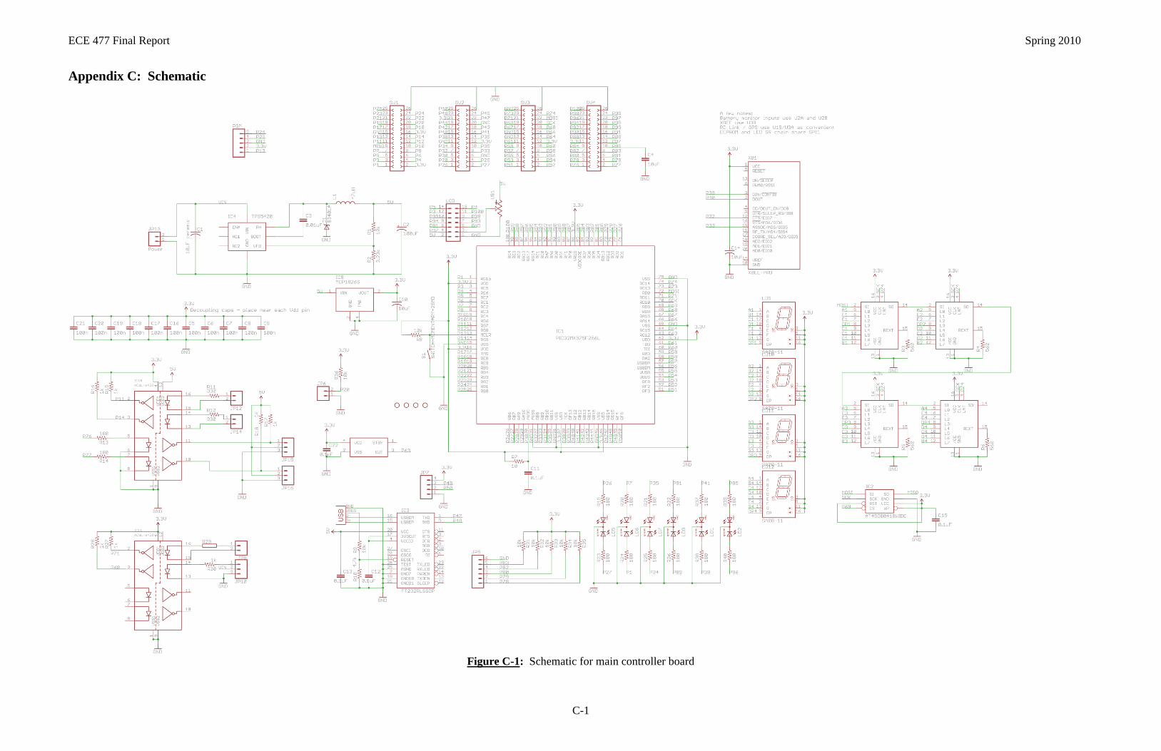
ECE 477 Final Report Spring 2010
C-1
Appendix C: Schematic
Figure C-1: Schematic for main controller board

ECE 477 Final Report Spring 2010
C-2
Figure C-2: Schematic for battery monitoring boards

ECE 477 Final Report Spring 2010
D-1
Appendix D: PCB Layout Top and Bottom Copper
Figure D-1: Main Control Board Top Copper and Silkscreen

ECE 477 Final Report Spring 2010
D-2
Figure D-2: Main Control Board Bottom Copper and Silkscreen

ECE 477 Final Report Spring 2010
D-3
Figure D-3: Battery Monitoring Board Top Copper and Silkscreen
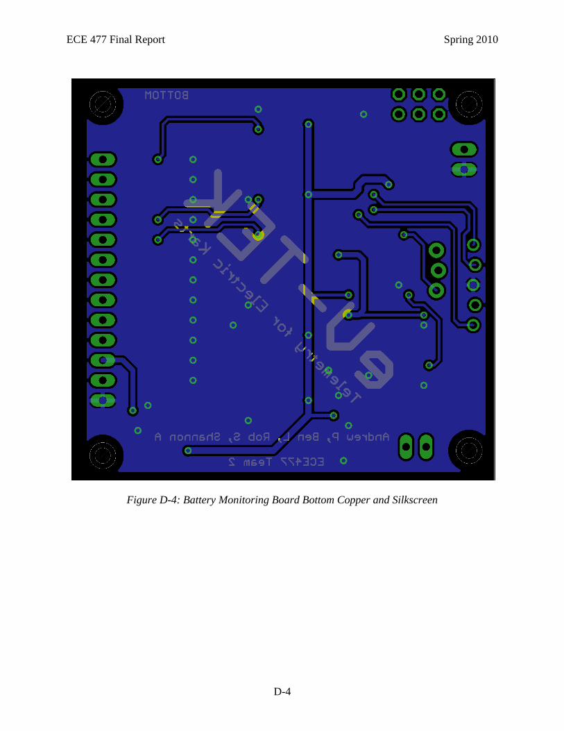
ECE 477 Final Report Spring 2010
D-4
Figure D-4: Battery Monitoring Board Bottom Copper and Silkscreen

ECE 477 Final Report Spring 2010
E-1
Appendix E: Parts List Spreadsheet
Vendor Manufacturer Part No. Description Unit Cost Qty Total Cost
Digi-Key STMicroelectronics LM324ADT IC Op Amp LP Quad 0.50 12 $6.00
Newark Microchip PIC18F4423 8-bit microcontroller IC 4.45 4 $17.80
Digi-Key Microchip PIC32MX575F256L 32-bit microcontroller IC 9.52 1 9.52
Mouser Hammond 1591XXLSFLBK Battery monitor package – plastic case 3.84 5 19.20
Mouser Hammond 1554V2GYCL Main board package – plastic case 34.68 1 34.68
Mouser Hantronix HDM24216H LCD character display 11.73 1 11.73
Mouser Digi Intl. Zigbee XBP09-DMUIT-156 900MHz Xbee Pro wireless module 39.00 1 39.00
Digi-Key - TGHGCR0100FE-ND .01 Ohm current sense resistor 27.21 4 108.84
Sparkfun Venus GPS-09133 GPS module 49.95 1 49.95
Sparkfun - ROB-09064
Servo motor 12.95 2 25.90
Silver Circuits Silver Circuits - Battery Monitor PCB 4.92 24 118.00
Advanced Circuits Advanced Circuits - Main Board PCB - - -
Batteries Plus Werker SLAA12-3.3F 12V 3.3AH main board battery 29.95 1 29.95
Various Various Various Miscellaneous resistors, capacitors,
inductors, LEDs, and connectors
- - 403.58
TOTAL $874.15

ECE 477 Final Report Spring 2010
F-1
Appendix F: FMECA Worksheet Subsystem A: Battery monitor power supply and reference voltage generator
Failure
No.
Failure Mode Possible Causes Failure Effects Method of
Detection
Criticality Remarks
A1 Supply voltage >
5V
Damaged 5V
regulator
Increased power
dissipation or
permanent failure
of battery monitor
Measurement of
supply voltages
Medium Can damage most
components on board
A2 Low/no supply
voltage
Damaged 5V
regulator, shorted
decoupling capacitor
Loss of battery
monitor
functionality
Measurement,
observation
Low
A3 Incorrect
reference voltages
Damaged reference
voltage ICs, shorted
bypass capacitor(s)
Consistently
incorrect voltage
readings from
circuit
Measurement of
reference
voltages,
observation
Low

ECE 477 Final Report Spring 2010
F-2
Subsystem B: Battery monitoring microcontroller
Failure
No.
Failure Mode Possible Causes Failure Effects Method of
Detection
Criticality Remarks
B1 Low voltage on
MCLR line
Missing/damaged
pull-up resistor
Erratic
microcontroller
operation,
sporadic
communication
with main board
Measurement of
MCLR pin
voltage, visual
inspection,
observation of
operation
Low
B2 Stuck output Damaged
microcontroller IC,
shorting of output pin
to power rail,
software
No
communication
with main board
Measurement of
serial output pin
Medium Possible damage to
battery microcontroller
B3 Shorted input pin Previous overvoltage
or overcurrent on
input pin, software
No ability to
measure voltage
or current
Measurement of
input pins
Medium Can possibly damage
op-amps or external
ADC

ECE 477 Final Report Spring 2010
F-3
Subsystem C: Battery measurement voltage followers
Failure
No.
Failure Mode Possible Causes Failure Effects Method of
Detection
Criticality Remarks
C1 Overvoltage at
operational
amplifier inputs
Missing/failed pull-
down resistor at non-
inverting input
Extremely high
battery voltage
readings
Measurement of
voltage follower
input voltage,
visual
inspection
Medium Possible damage to
operational amplifiers
C2 Zero voltage at
operational
amplifier inputs
Missing/failed
voltage divider
resistor(s)
Extremely low
battery voltage
readings; system
insistence that all
batteries are dead
Measurement of
voltage follower
inputs, visual
inspection
Low
C3 General op-amp
failure
Defective ICs,
previous overvoltage
condition
Erratic/random
voltage/current
readings
Observation Low

ECE 477 Final Report Spring 2010
F-4
Subsystem D: Main controller board power supply
Failure
No.
Failure Mode Possible Causes Failure Effects Method of
Detection
Criticality Remarks
D1 Zero output on
5V rail
Damaged 5V
regulator, damaged
inductor, shorted
bulk/decoupling
capacitor, damaged
feedback components
No operation of
main board,
excessive drain
from main board
supply battery
Measurement,
observation
Medium Possible damage to 5V
regulator or inductor
D2 5V rail > 5V Damaged 5V
regulator, damaged
feedback network
Increased main
board power
dissipation,
possible
component failure
Measurement Medium
D3 Zero output on
3.3V rail
Damaged 3.3V
regulator, shorted
bulk/decoupling
capacitor
No operation of
main board
except LCD,
USB, and servos
Measurement,
observation
Medium Possible damage to 5V
regulator, inductor, or
3.3V regulator
D4 3.3V rail > 3.3V Damaged 3.3V
regulator
Increased main
board power
dissipation,
possible
component failure
Measurement Medium
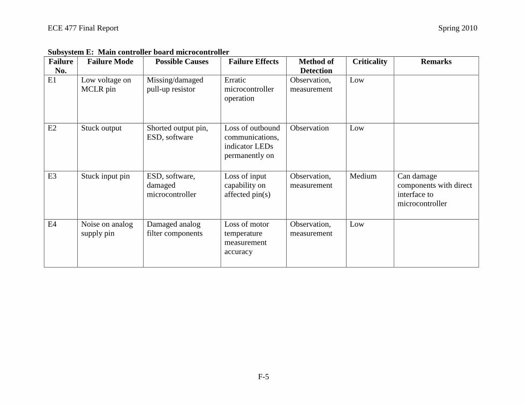
ECE 477 Final Report Spring 2010
F-5
Subsystem E: Main controller board microcontroller
Failure
No.
Failure Mode Possible Causes Failure Effects Method of
Detection
Criticality Remarks
E1 Low voltage on
MCLR pin
Missing/damaged
pull-up resistor
Erratic
microcontroller
operation
Observation,
measurement
Low
E2 Stuck output Shorted output pin,
ESD, software
Loss of outbound
communications,
indicator LEDs
permanently on
Observation Low
E3 Stuck input pin ESD, software,
damaged
microcontroller
Loss of input
capability on
affected pin(s)
Observation,
measurement
Medium Can damage
components with direct
interface to
microcontroller
E4 Noise on analog
supply pin
Damaged analog
filter components
Loss of motor
temperature
measurement
accuracy
Observation,
measurement
Low

ECE 477 Final Report Spring 2010
F-6
Subsystem F: Optically-isolated interfaces
Failure
No.
Failure Mode Possible Causes Failure Effects Method of
Detection
Criticality Remarks
F1 High voltage
(over 5V) on
output pin
Failure of isolation Immediate and
extensive damage
to main board
components
Observation Medium
F2 No signals cross
isolation barrier
Open circuit in
emitter loop (resistor
failure)
Loss of
communication
across optical
isolators
Observation Low
F3 Overcurrent into
emitters
Current-limiting
resistor failed shorted
Excessive power
dissipation in
optoisolators
Measurement Medium Possible damage to
optical emitters
F4 Ouput pin stuck
at logic „1‟
Shorted pullup
resistor
Excessive power
dissipation in
output driver of
isolator
Measurement Medium Possible damage to
output drivers

ECE 477 Final Report Spring 2010
F-7
Subsystem G: USB controller circuit
Failure
No.
Failure Mode Possible Causes Failure Effects Method of
Detection
Criticality Remarks
G1 Constant voltage
on output pin
ESD, previous
overcurrent/overvoltage
event
Loss of
communication
with host PC
Measurement,
Observation
Low
G2 Constant low
voltage (logic
„0‟) on reset pin
Open R9 or shorted
R10
Loss of
communication
with host PC
Measurement,
observation
Low
G3 Constant high
voltage (logic
„1‟) on reset pin
Shorted R9 or open
R10
Failure to
properly initialize
IC upon USB
connection; loss
of communication
with host PC
Measurement,
observation
Low
Related Documents

![ZigBee RF4CE Stack User Guide - NXP Semiconductors · 094945r00ZB ZigBee RF4CE Specification [ZigBee Alliance document] 094950r00ZB ZigBee RF4CE Device Type List [ZigBee Alliance](https://static.cupdf.com/doc/110x72/5f168d2f412bb13bb1076764/zigbee-rf4ce-stack-user-guide-nxp-semiconductors-094945r00zb-zigbee-rf4ce-specification.jpg)