EE 4271 VLSI Design, Fall 2011 CMOS Combinational Gate

EE 4271 VLSI Design, Fall 2011 CMOS Combinational Gate.
Dec 20, 2015
Welcome message from author
This document is posted to help you gain knowledge. Please leave a comment to let me know what you think about it! Share it to your friends and learn new things together.
Transcript
EE 4271 VLSI Design, Fall 2011
CMOS Combinational Gate
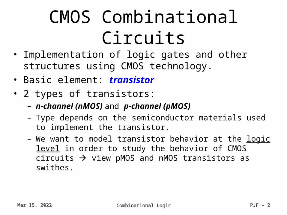
CMOS Combinational Circuits• Implementation of logic gates and other structures using CMOS
technology.• Basic element: transistor• 2 types of transistors:
– n-channel (nMOS) and p-channel (pMOS)– Type depends on the semiconductor materials used to implement the
transistor.– We want to model transistor behavior at the logic level in order to study
the behavior of CMOS circuits view pMOS and nMOS transistors as swithes.
Apr 18, 2023Apr 18, 2023 Combinational LogicCombinational Logic PJFPJF - - 22

CMOS transistors as Switches
Apr 18, 2023Apr 18, 2023 Combinational LogicCombinational Logic PJFPJF - - 33
3 terminals in CMOS transistors: G: Gate D: Drain S: Source
nMOS transistor/switch X=1 switch closes (ON) X=0 switch opens (OFF)
pMOS transistor/switch X=1 switch opens (OFF) X=0 switch closes (ON)

Networks of Switches
• Use switches to create networks that represent CMOS logic circuits.
• To implement a function F, create a network s.t. there is a path through the network whenever F=1 and no path when F=0.
• Two basic structures:– Transistors in Series– Transistors in Parallel
Apr 18, 2023Apr 18, 2023 Combinational LogicCombinational Logic PJFPJF - - 44
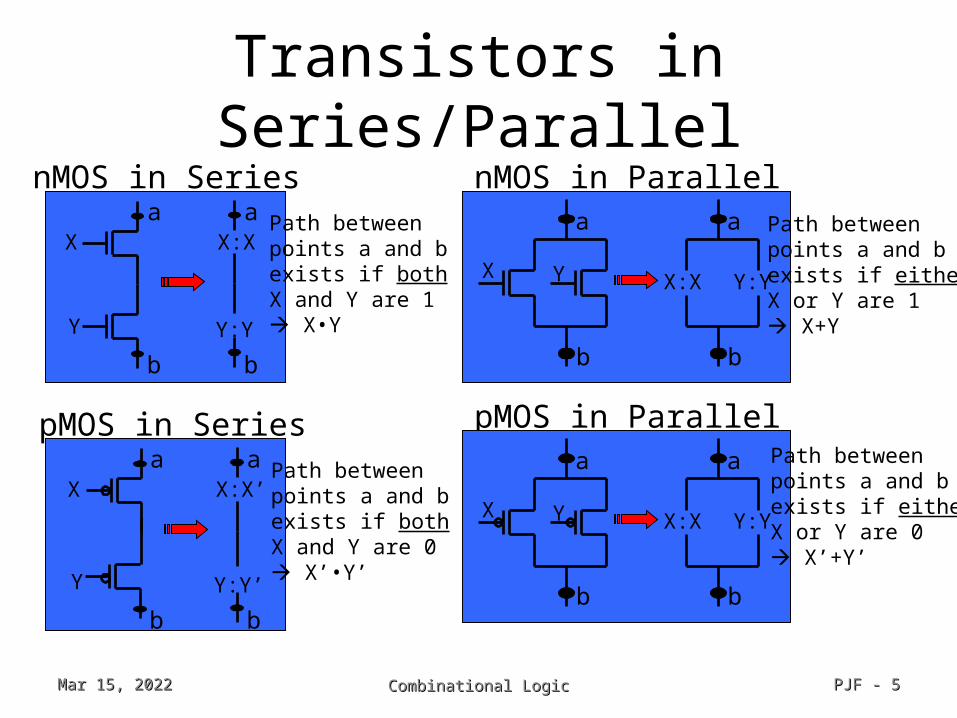
Transistors in Series/Parallel
Apr 18, 2023Apr 18, 2023 Combinational LogicCombinational Logic PJFPJF - - 55
nMOS in ParallelnMOS in Series
X
Y
a
b
X:X
Y:Y
a
b
pMOS in Series
X
Y
a
b
X:X’
Y:Y’
a
b
Path between points a and b exists if both X and Y are 1 X•Y
Path between points a and b exists if both X and Y are 0 X’•Y’
Path between points a and b exists if either X or Y are 1 X+Y
X Y
b
a
X:X Y:Y
b
a
pMOS in Parallel
X Y
b
a
X:X Y:Y
b
a Path between points a and b exists if either X or Y are 0 X’+Y’
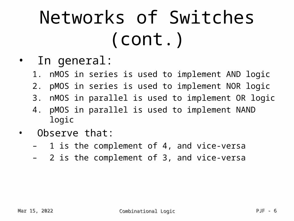
Networks of Switches (cont.)
• In general:1. nMOS in series is used to implement AND logic2. pMOS in series is used to implement NOR logic3. nMOS in parallel is used to implement OR logic4. pMOS in parallel is used to implement NAND logic
• Observe that:– 1 is the complement of 4, and vice-versa– 2 is the complement of 3, and vice-versa
Apr 18, 2023Apr 18, 2023 Combinational LogicCombinational Logic PJFPJF - - 66
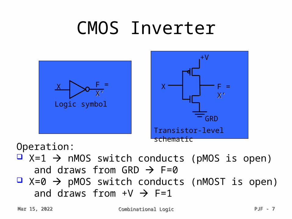
CMOS Inverter
Apr 18, 2023Apr 18, 2023 Combinational LogicCombinational Logic PJFPJF - - 77
X F = X’X’
Logic symbol
X F = X’X’
+V
GRD
Transistor-level schematic
Operation: X=1 nMOS switch conducts (pMOS is open) and draws from GRD F=0 X=0 pMOS switch conducts (nMOST is open) and draws from +V F=1
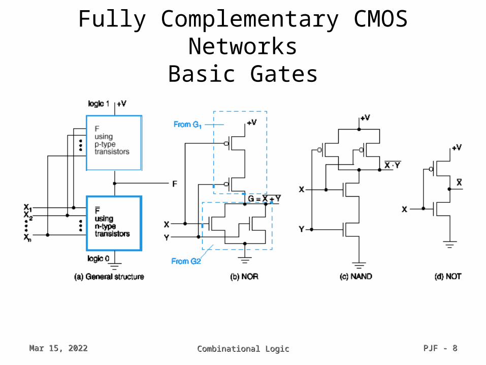
Fully Complementary CMOS NetworksBasic Gates
Apr 18, 2023Apr 18, 2023 Combinational LogicCombinational Logic PJFPJF - - 88
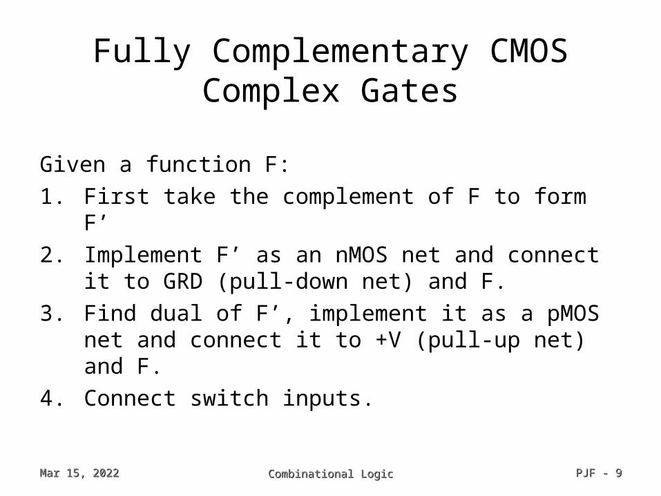
Fully Complementary CMOSComplex Gates
Given a function F:1. First take the complement of F to form F’2. Implement F’ as an nMOS net and connect it to GRD (pull-
down net) and F.3. Find dual of F’, implement it as a pMOS net and connect it
to +V (pull-up net) and F.4. Connect switch inputs.
Apr 18, 2023Apr 18, 2023 Combinational LogicCombinational Logic PJFPJF - - 99
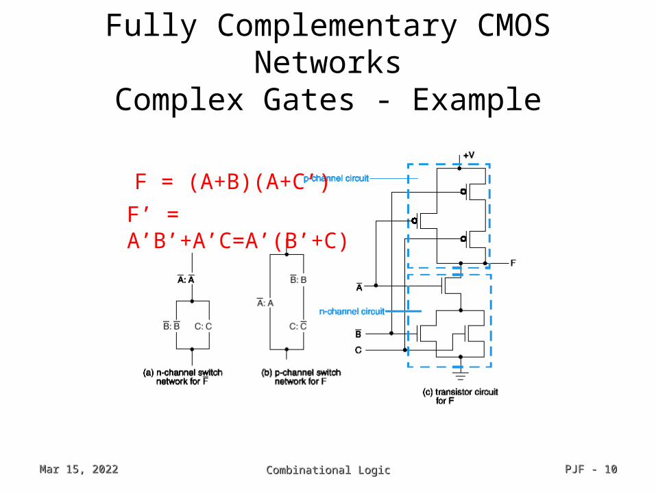
Fully Complementary CMOS NetworksComplex Gates - Example
Apr 18, 2023Apr 18, 2023 Combinational LogicCombinational Logic PJFPJF - - 1010
F’ = A’B’+A’C=A’(B’+C)
F = (A+B)(A+C’)

CMOS Transmission Gate (TG)
Apr 18, 2023Apr 18, 2023 Combinational LogicCombinational Logic PJFPJF - - 1111
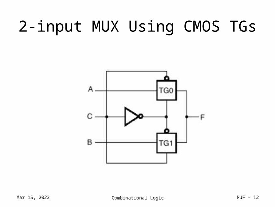
2-input MUX Using CMOS TGs
Apr 18, 2023Apr 18, 2023 Combinational LogicCombinational Logic PJFPJF - - 1212
Related Documents


![EE415 VLSI Design COMBINATIONAL LOGIC [Adapted from Rabaeys Digital Integrated Circuits, ©2002, J. Rabaey et al.]](https://static.cupdf.com/doc/110x72/5519b7875503465b578b4854/ee415-vlsi-design-combinational-logic-adapted-from-rabaeys-digital-integrated-circuits-2002-j-rabaey-et-al.jpg)