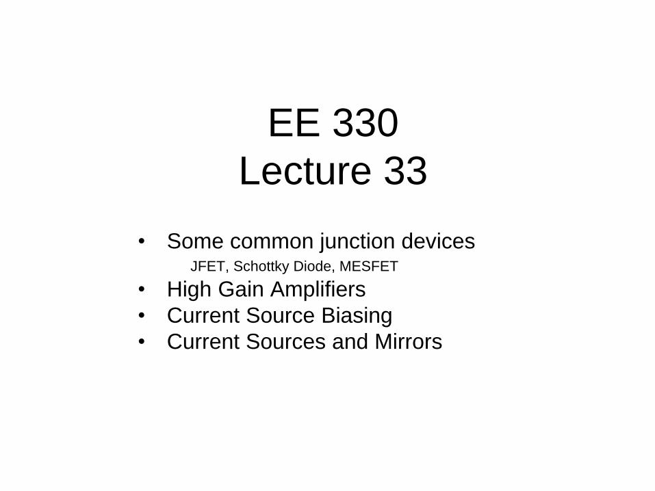
EE 330 Lecture 33 • Some common junction devices JFET, Schottky Diode, MESFET • High Gain Amplifiers • Current Source Biasing • Current Sources and Mirrors

Welcome message from author
This document is posted to help you gain knowledge. Please leave a comment to let me know what you think about it! Share it to your friends and learn new things together.
Transcript
EE 330
Lecture 33
• Some common junction devicesJFET, Schottky Diode, MESFET
• High Gain Amplifiers
• Current Source Biasing
• Current Sources and Mirrors

Additional Lecture Postings
Lectures Numbered 31 and 32 will be posted along with streams
from Spring 2020 but except for what is discussed today on the
topic of “Some Common Junction Devices”, students will not be
held responsible for the material. Major emphasis on these two
lectures is Thyristors. This material is normally covered in this
course in the typical 15-week semester but due to the pandemic
and the corresponding shortening to a 14-week semester, this
material will not be covered in the class.

Exam 3 Friday Nov 6
Final Mon Nov 23 (scheduled 2:15 pm)
Exams 2 and 3 will be posted on Canvas by 9:00 AM on the day of
exam and due at 1:00 PM
Final Exam will be posted on Canvas by 10:00 AM on the day of exam
and due at 4:15 PM
???
???
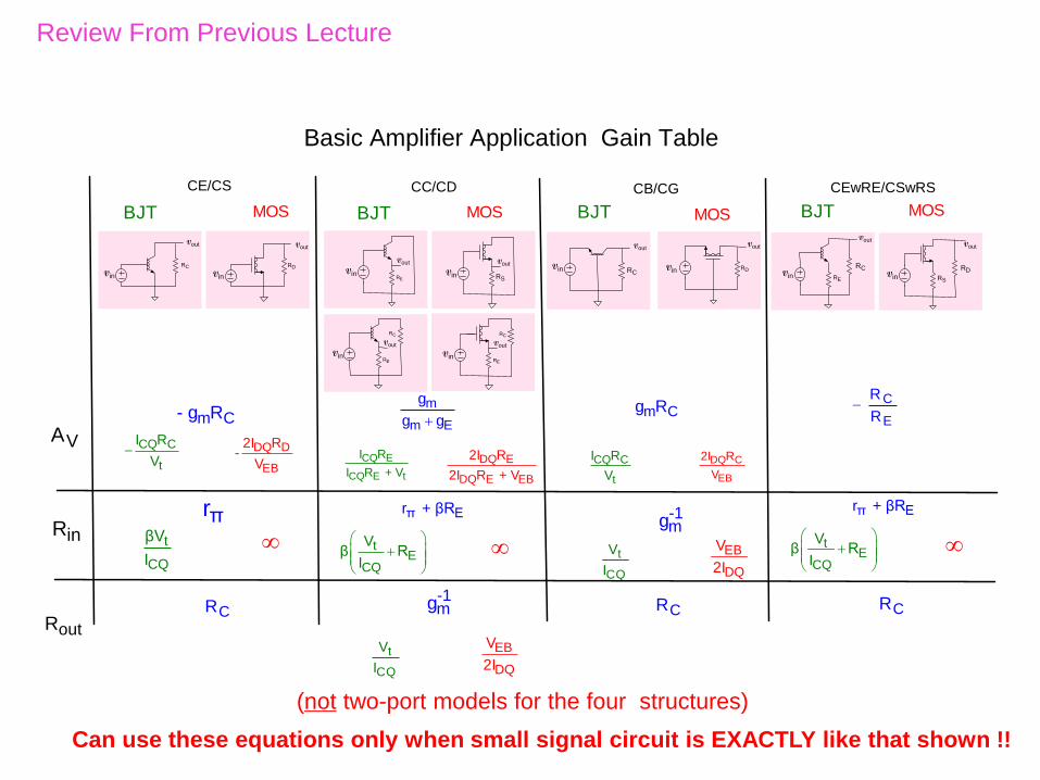
(not two-port models for the four structures)
m C- g R m C g Rm
m E
g
g g
C
E
R
R
DQ C
EB
2I R
V
DQ E
DQ E EB
2I R
2I R + V
DQ D
EB
2I R-
V
CQ C
t
I R
V
CQ C
t
I R
V
CQ E
CQ E t
I R
I R + V
π r π E r + βR
-1m g
t
CQ
βV
It
ECQ
Vβ R
I
t
CQ
V
I
EB
DQ
V
2I
MOS BJT
in V
out V
D R in V
out V
C R in V
out V
E R in V
out V
S R
CE/CS
in V
out V
C R
in V
out V
D R
in V
out V
E R
C R
in V
out V
S R
D R
CC/CD CB/CG CEwRE/CSwRS
CR
-1m g
t
CQ
V
I
EB
DQ
V
2I
CR
π E r + βR
tE
CQ
Vβ R
I
CR
MOS BJT MOS BJT MOS BJT
V A
in R
out R
Basic Amplifier Application Gain Table
in V out V
E R
C R
in V out V
E R
C R
Can use these equations only when small signal circuit is EXACTLY like that shown !!
Review From Previous Lecture
B
E
C
VDD
Vin
RC
Vout
RE
VEE
B
E
C
VSS
VDD
Vin
RE
Vout
B
E
C
VDD
Vin
RC
Vout
VEE
B
E
C
VBB
VDD
Vin
RC
Vout
CE/CS
CC/CD
CB/CG
CEwRE/
CSwRS
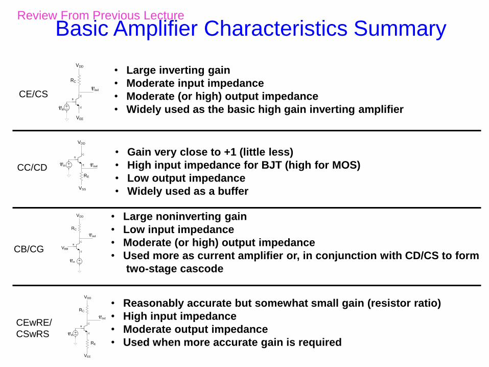
Basic Amplifier Characteristics Summary
• Reasonably accurate but somewhat small gain (resistor ratio)
• High input impedance
• Moderate output impedance
• Used when more accurate gain is required
• Large noninverting gain
• Low input impedance
• Moderate (or high) output impedance
• Used more as current amplifier or, in conjunction with CD/CS to form
two-stage cascode
• Large inverting gain
• Moderate input impedance
• Moderate (or high) output impedance
• Widely used as the basic high gain inverting amplifier
• Gain very close to +1 (little less)
• High input impedance for BJT (high for MOS)
• Low output impedance
• Widely used as a buffer
Review From Previous Lecture

Review: Small-signal equivalent of a one-port
VIN
Linear One-Port
Facing Input
RIN
“Diode-connected transistor”
0m mg g g g
0
1 1
m m
Rg g g
0g g
0
1R
g
Review From Previous Lecture

Review: Small-signal equivalent of a one-port
VIN
Linear One-Port
Facing Input
RIN
“Diode-connected transistor”
0m mg g g g g
0
1 1
m m
Rg g g g
0g g
0
1R
g
Review From Previous Lecture
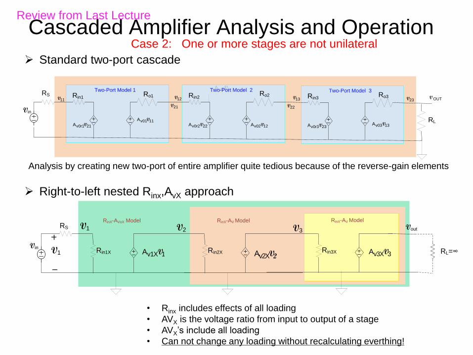
Cascaded Amplifier Analysis and Operation
Ro1
v0 1A V
Rin1
v0r1 21A V
Two-Port Model 1Ro2
v02 12A V
Rin2
v0r2 22A V
Two-Port Model 2Ro3
v03 13A V
Rin3
v0r3 23A V
Two-Port Model 3
RL
OUT V23 V13 V
22 V
12 V
21 V
v01 11A V
11 VRS
Vin
Analysis by creating new two-port of entire amplifier quite tedious because of the reverse-gain elements
Right-to-left nested Rinx,AvX approach
Standard two-port cascade
• Rinx includes effects of all loading
• AVX is the voltage ratio from input to output of a stage
• AVX’s include all loading
• Can not change any loading without recalculating everthing!
V1 v1X 1A VRin1X
Vin
RS
RinX-AVoX Model
v3X 3A VRin3X
RinX-AV Model
Vout
RL=∞v2XA 2VRin2X
RinX-AV Model
V3V2V1
Case 2: One or more stages are not unilateral
Review from Last Lecture
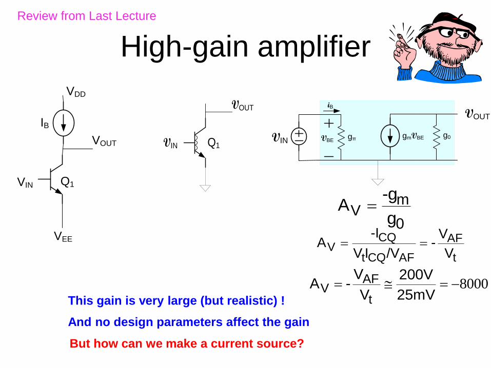
High-gain amplifier
VIN
VOUT
Q1
VDD
VEE
IB
VIN
VOUT
Q1
mV
0
-gA
g
gmVBEVBE
iB
gπg0VIN
VOUT
CQ AFV
t CQ AF t
-I VA -
V I /V V
8000AFV
t
V 200VA -
V 25mV
This gain is very large (but realistic) !
But how can we make a current source?
And no design parameters affect the gain
Review from Last Lecture
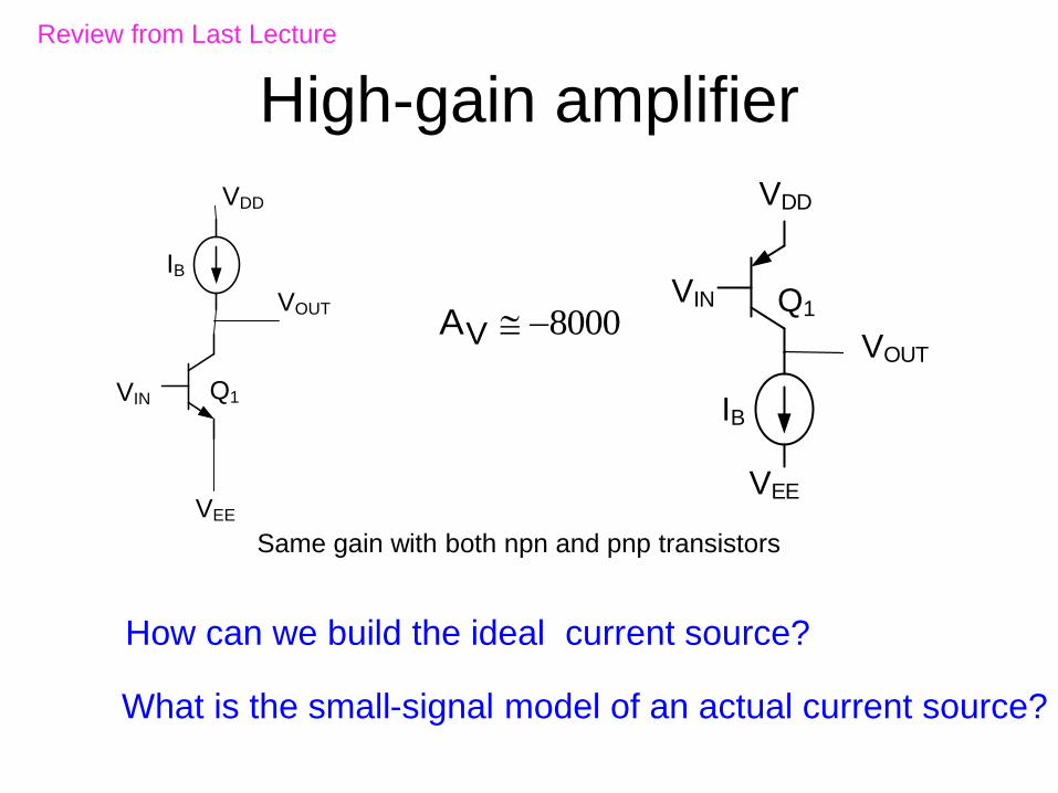
High-gain amplifier
VIN
VOUT
Q1
VDD
VEE
IB
8000VA
How can we build the ideal current source?
What is the small-signal model of an actual current source?
VIN
VOUT
Q1
VDD
VEE
IB
Same gain with both npn and pnp transistors
Review from Last Lecture

Some common junction devices
JFET
Schottky Diode
MESFET
Compatible with standard processes, usually with small number of
additional processing steps
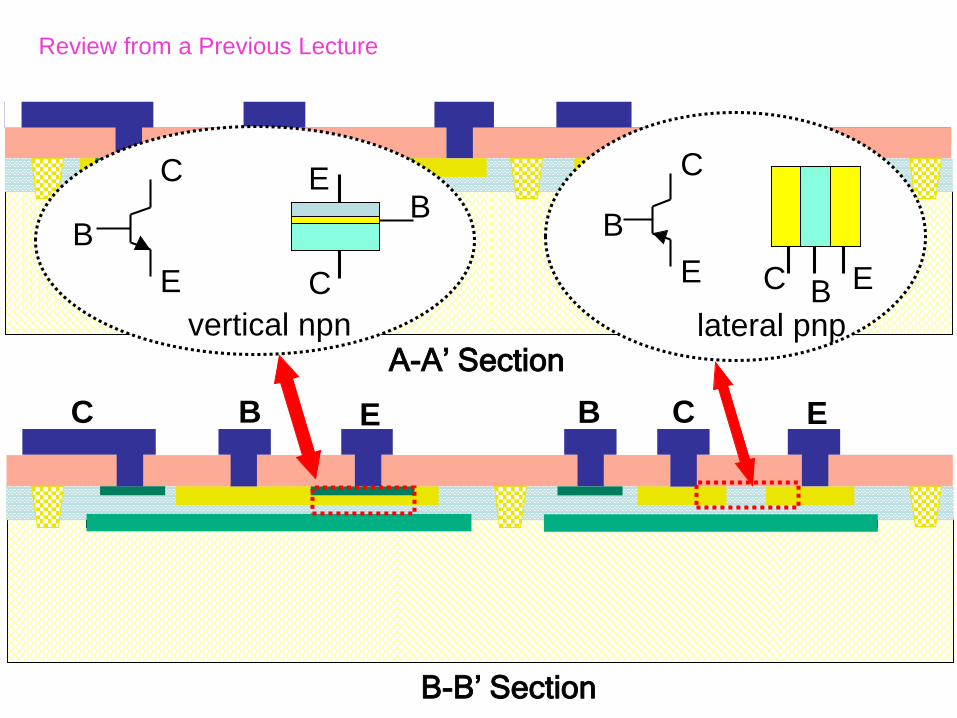
A-A’ Section
B-B’ Section
E
C
B
vertical npn
B
C
E
E
B
C
EC Blateral pnp
C B E B C E
Review from a Previous Lecture
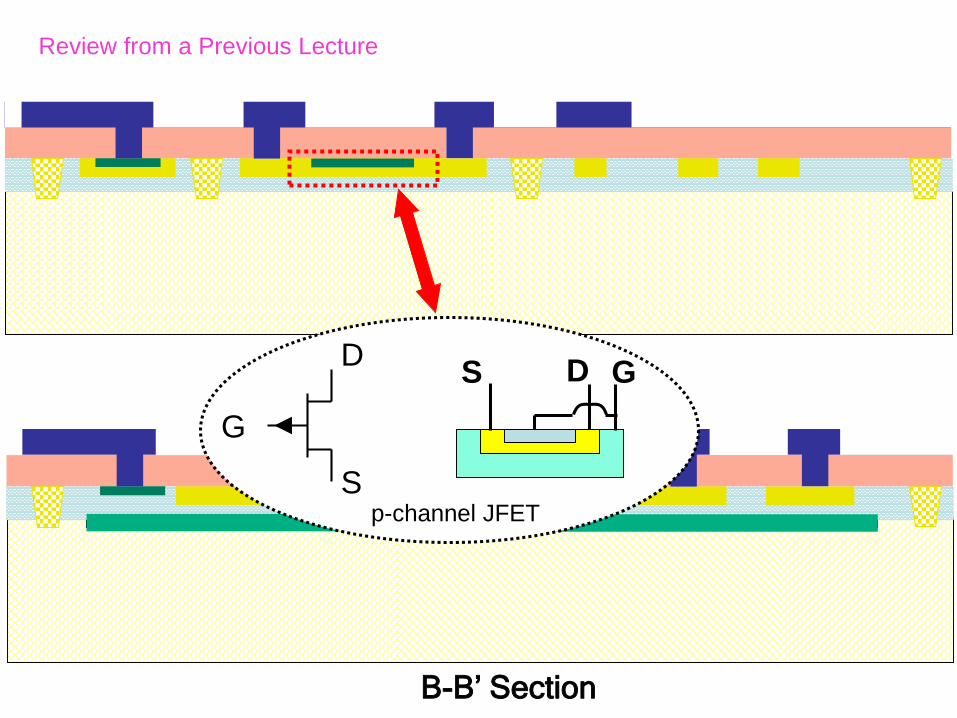
A-A’ Section
B-B’ Section
GDS
S
D
G
p-channel JFET
Review from a Previous Lecture

BE
C
E
B
C
EC Blateral pnp
E
C
B
vertical npn
B
C
E
E C
B
Review from a Previous Lecture

L
G
DS
W
Resistor
Diode (capacitor)
GDS
S
D
G
p-channel JFET
Review from a Previous Lecture

Enhancement and Depletion MOS Devices
• Enhancement Mode n-channel devices
VT > 0
• Enhancement Mode p-channel devices
VT < 0
• Depletion Mode n-channel devices
VT < 0
• Depletion Mode p-channel devices
VT > 0
Will consider the JFET but first some
additional information about MOS Devices

Enhancement and Depletion MOS Devices
• Depletion mode devices require only one additional mask step
• Older n-mos and p-mos processes usually had a depletion device and an
enhancement device
• Depletion devices usually not available in CMOS because applications usually
do not justify the small increasing costs in processing
• The threshold voltage of either n-channel or p-channel devices is adjusted to a
desired value by doing a channel implant before gate oxide is applied
n-channel p-channel
Enhancement
Depletion

The JFET
Under sufficiently large reverse bias (depletion region widens and channel
disappears - “pinches off”)
SD
G
With VGS=0, channel exists under gate between D and S
SD
GVGS
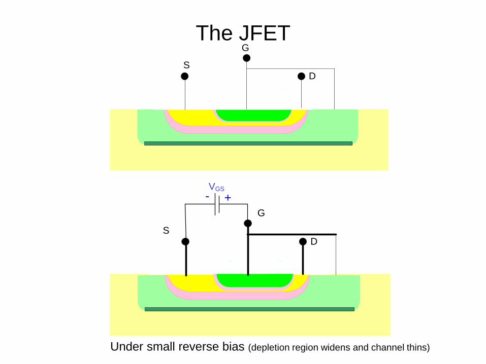
The JFET
SD
G
Under small reverse bias (depletion region widens and channel thins)
SD
G
VGS
+-

The JFET
Under small reverse bias and large negative VDS (channel pinches off)
SD
G
SD
G
VGS
VDS+
+
-
-

The JFET
SD
G
0.3
0.3
GS P
DSSp DSD GS P DS GS P DS GS P2
P
2
GSDSSp GS P DS G
P
GS
S P
0 V V
2I VI V -V - V V V V > V -V
V 2
VI 1- V V V < V -V
V
V +0.3
D D
S S
G G
n-channel p-channelp-channel JFET
Square-law model of p-channel JFET
• Functionally identical to the square-law model of MOSFET
• Parameters IDSS and VP characterize the device
• IDSS proportional to W/L where W and L are width and length of n+ diff
• VP is negative for n-channel device, positive for p-channel device thus JFET is depletion mode device
• Must not forward bias GS junction by over about 300mV or excessive base current will flow (red constraint)
• Widely used as input stage for bipolar op amps
(IDSSp carries negative sign)

The JFET
0.3 0.3
0.3
GS P
DSS DSD GS P DS GS P DS GS P2
P
2
GSDSS GS P DS GS P
P
0 V V
2I VI V -V - V V V V < V -V
V 2
VI 1- V V V
V
> V -VV
GS
D D
S S
G G
n-channel p-channel
n-channel JFET
Square-law model of n-channel JFET
• Functionally identical to the square-law model of MOSFET
• Parameters IDSS and VP characterize the device
• IDSS proportional to W/L where W and L are width and length of n+ diff
• VP is negative for n-channel device, positive for p-channel device thus JFET is depletion mode device
• Must not forward bias GS junction by over about 300mV or excessive base current will flow (red constraint)
• Widely used as input stage for bipolar op amps
(not available in this process)
SD
G
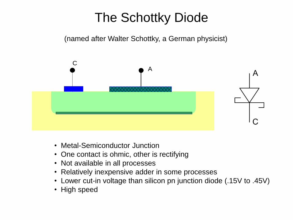
The Schottky Diode
CA
• Metal-Semiconductor Junction
• One contact is ohmic, other is rectifying
• Not available in all processes
• Relatively inexpensive adder in some processes
• Lower cut-in voltage than silicon pn junction diode (.15V to .45V)
• High speed
(named after Walter Schottky, a German physicist)
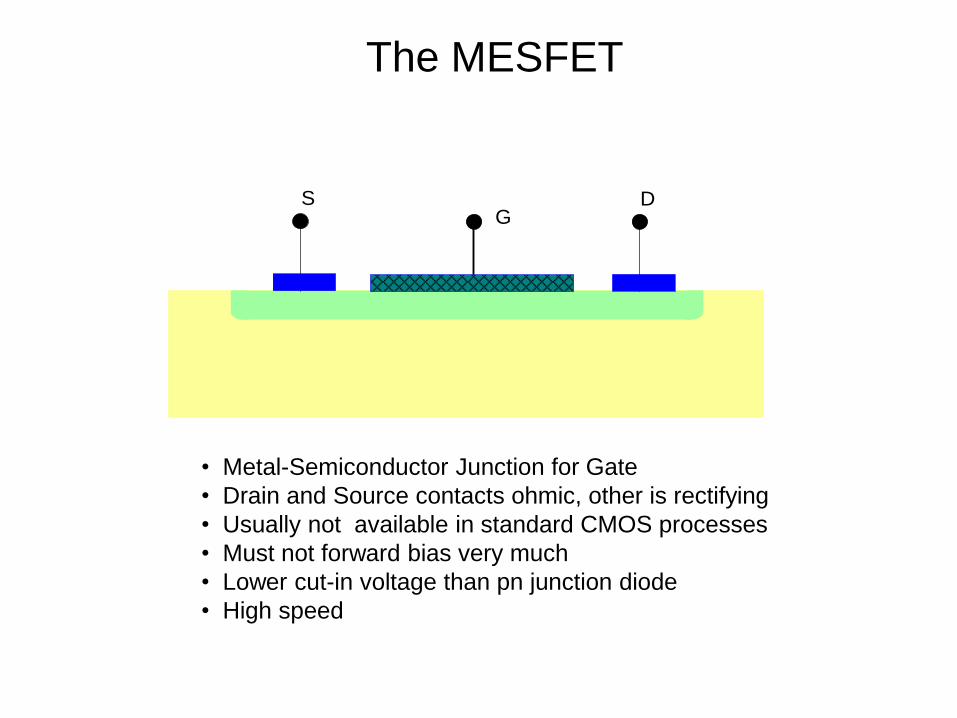
The MESFET
SG
D
• Metal-Semiconductor Junction for Gate
• Drain and Source contacts ohmic, other is rectifying
• Usually not available in standard CMOS processes
• Must not forward bias very much
• Lower cut-in voltage than pn junction diode
• High speed
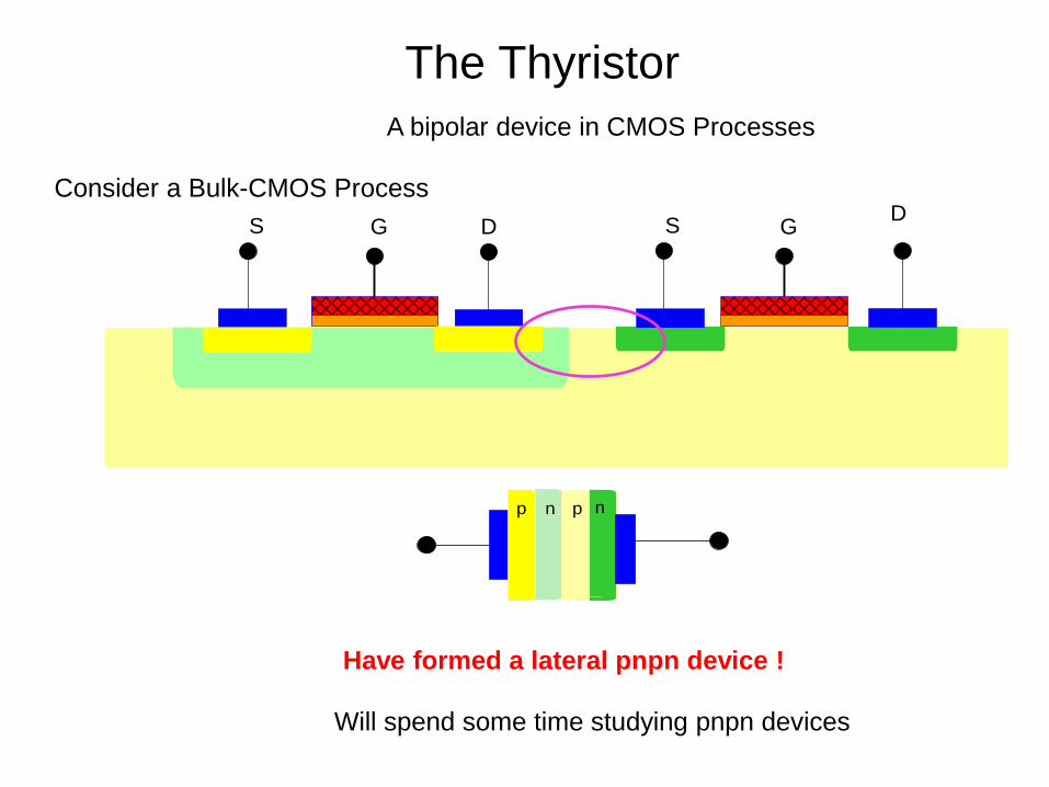
The Thyristor
S G D GSD
Consider a Bulk-CMOS Process
A bipolar device in CMOS Processes
p pn n
Have formed a lateral pnpn device !
Will spend some time studying pnpn devices
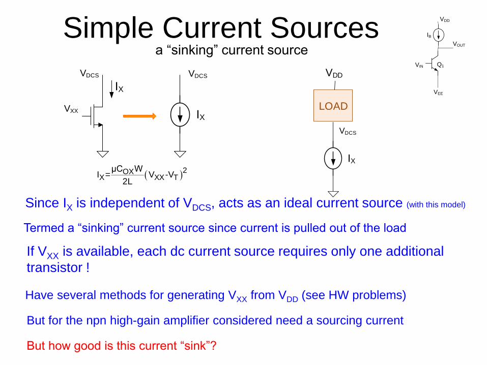
Simple Current SourcesVIN
VOUT
Q1
VDD
VEE
IB
Since IX is independent of VDCS, acts as an ideal current source (with this model)
If VXX is available, each dc current source requires only one additional
transistor !
VXX
IX
IX
2OX
X XX TμC W
I = V -V2L
VDCS VDCS
Have several methods for generating VXX from VDD (see HW problems)
But for the npn high-gain amplifier considered need a sourcing current
Termed a “sinking” current source since current is pulled out of the load
IX
VDCS
VDD
LOAD
But how good is this current “sink”?
a “sinking” current source
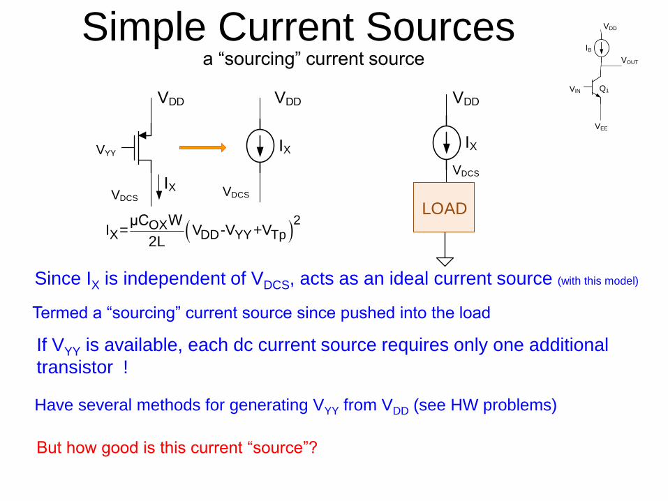
Simple Current Sources
VIN
VOUT
Q1
VDD
VEE
IB
Since IX is independent of VDCS, acts as an ideal current source (with this model)
If VYY is available, each dc current source requires only one additional
transistor !
Have several methods for generating VYY from VDD (see HW problems)
Termed a “sourcing” current source since pushed into the load
But how good is this current “source”?
a “sourcing” current source
IX
VDD
VDCS
LOAD
VYY
IX
IX
2OX
X DD YY TpμC W
I = V -V +V2L
VDD VDD
VDCSVDCS

Simple Current SourcesVIN
VOUT
Q1
VDD
VEE
IB
Since IX is independent of VCCS, acts as an ideal current source (with this model)
If VXX is available, each dc current source requires only one additional
transistor !
Have several methods for generating VXX from VDD (see HW problems)
But for the npn high-gain amplifier considered need a sourcing current
Termed a “sinking” current source since current is pulled out of the load
IX
VCCS
VDD
LOAD
But how good is this current “sink”?
a “sinking” current source
VXX
IX IX
XX
t
V
VX S EI = J A e
VCCS VCCS
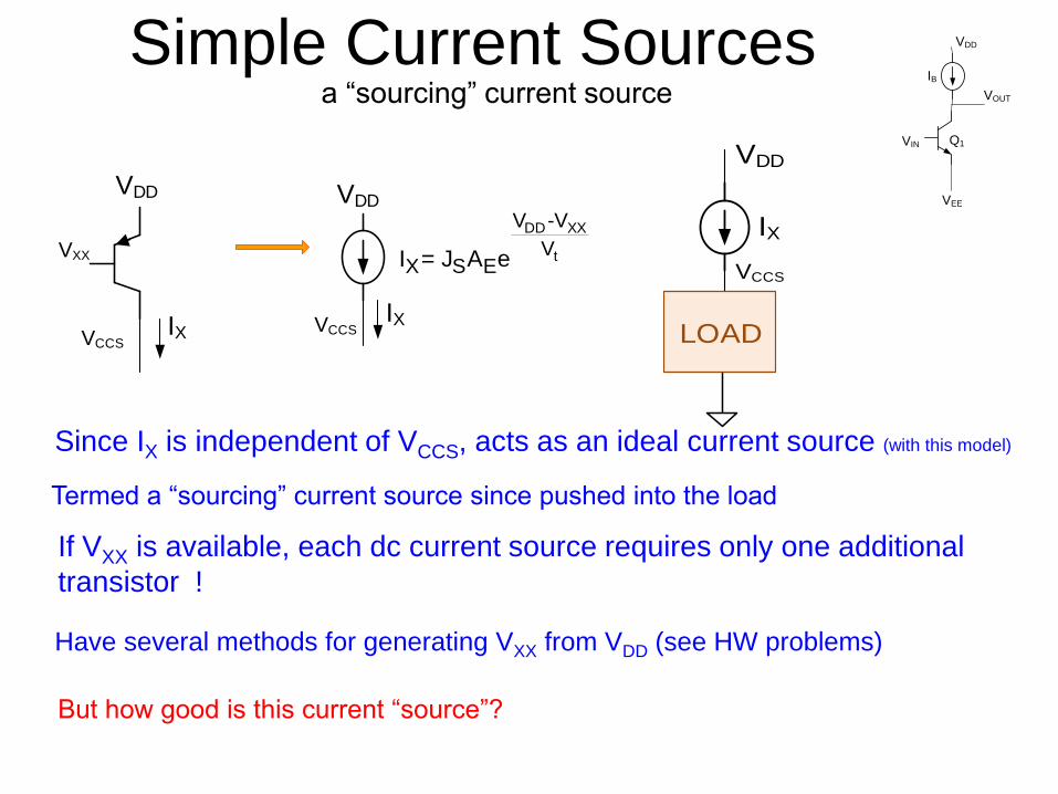
Simple Current Sources
VIN
VOUT
Q1
VDD
VEE
IB
Since IX is independent of VCCS, acts as an ideal current source (with this model)
If VXX is available, each dc current source requires only one additional
transistor !
Have several methods for generating VXX from VDD (see HW problems)
Termed a “sourcing” current source since pushed into the load
But how good is this current “source”?
a “sourcing” current source
IX
VDD
VCCS
LOAD
VXX
IXIX
DD XX
t
V -V
VX S EI = J A e
VDD VDD
VCCS
VCCS
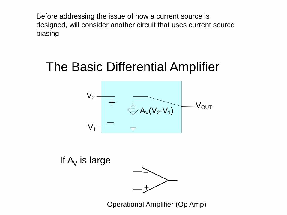
Before addressing the issue of how a current source is
designed, will consider another circuit that uses current source
biasing
The Basic Differential Amplifier
V2
AV(V2-V1)
V1
VOUT
If AV is large
Operational Amplifier (Op Amp)

Example: Determine the voltage gain of the
following circuit
gm1VBE1VBE1
iB1
gπ1 gm2VBE2 VBE2
iB2
gπ2
RC1 RC1Vin
Vout
VE
Q1
Vin
-VEE
RC1
Q2
RC1
VDD
IEE
VOUT
AE1=AE2
Vout
Q1
Vin
RC1
Q2
RC1
AE1=AE2
VE
1 22
m mg g EE
t
I
V=
EEC1 C2
II = I
2=
Since symmetric when VIN=0
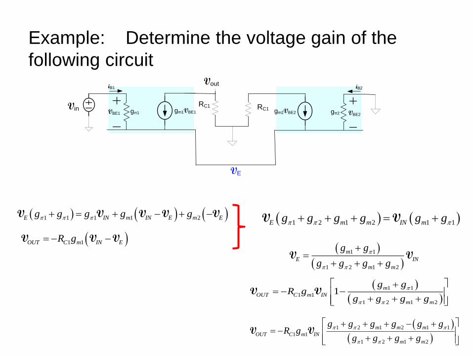
Example: Determine the voltage gain of the
following circuit
gm1VBE1VBE1
iB1
gπ1 gm2VBE2 VBE2
iB2
gπ2
RC1 RC1Vin
Vout
VE
1 1OUT C m IN ER g V V V
1 1 1 1 2E IN m IN E m Eg g g g g V V V V V 1 2 1 2 1 1E m m IN mg g g g g g V V
1 1
1 2 1 2
m
E IN
m m
g g
g g g g
V V
1 1
1 1
1 2 1 2
1m
OUT C m IN
m m
g gR g
g g g g
V V
1 2 1 2 1 1
1 1
1 2 1 2
m m m
OUT C m IN
m m
g g g g g gR g
g g g g
V V

Example: Determine the voltage gain of the
following circuit
gm1VBE1VBE1
iB1
gπ1 gm2VBE2 VBE2
iB2
gπ2
RC1 RC1Vin
Vout
VE
1 2 1 2 1 1
1 1
1 2 1 2
m m m
OUT C m IN
m m
g g g g g gR g
g g g g
V V
2
1 1
1 2
mOUT C m IN
m m
gR g
g gV V
1 1
2
C mOUT IN
R gV V
2OUTV
1 12
2
C mOUT IN
R gV V

Differential amplifier
Q1
Vin1
-VEE
RC1
Q2
RC1
VDD
IEE
VOUT1
AE1=AE2Vin2
VOUT2
1 11 1 2
2
C mOUT IN IN
R gV V V
1 12 1 2
2
C mOUT IN IN
R gV V V
• Very useful circuit
• This is a basic Op Amp
• Uses a current source and VDD for biasing (no biasing resistors or caps!)
• But – needs a dc current source !!!!
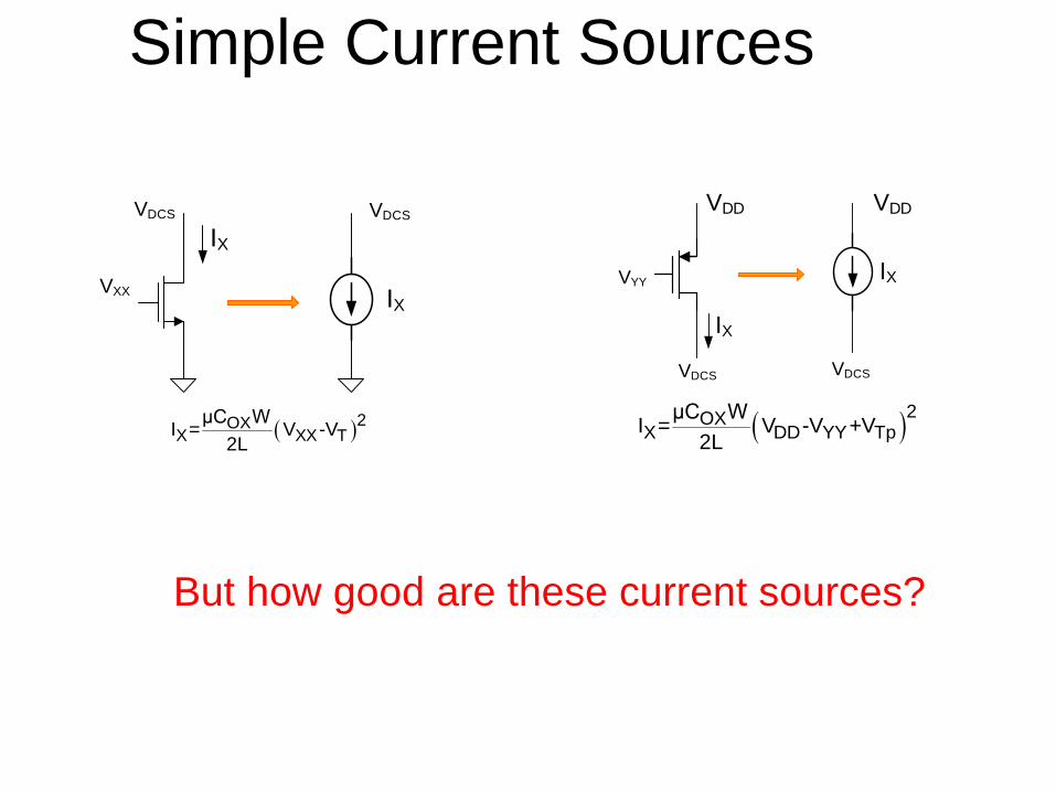
Simple Current Sources
But how good are these current sources?
VYY
IX
IX
2OX
X DD YY TpμC W
I = V -V +V2L
VDD VDD
VDCS VDCS
VXX
IX
IX
2OX
X XX TμC W
I = V -V2L
VDCS VDCS
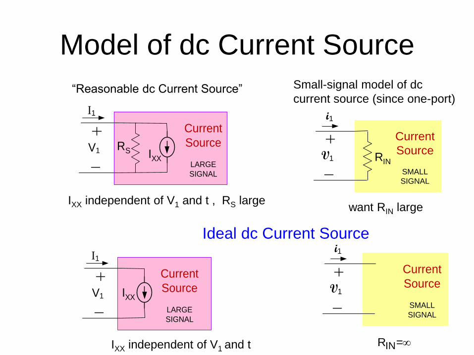
Model of dc Current Source
V1
I1
Current
Source
LARGE
SIGNAL
SRXXI V1
i1
Current
Source
SMALL
SIGNAL
INR
“Reasonable dc Current Source”
IXX independent of V1 and t , RS large
Small-signal model of dc
current source (since one-port)
want RIN large
Ideal dc Current Source
V1
I1
Current
Source
LARGE
SIGNAL
XXI V1
i1
Current
Source
SMALL
SIGNAL
IXX independent of V1 and t INR =

Current Sources/Mirrors
Q0
VCC
R
Q1
AE0 AE1
Lo
ad
I1I0
VXX
Q0
VCC
R
Q1
AE0 AE1
Lo
ad
I1I0
V1
I1
Current Source
Will show circuit in red behaves as a current source
R and Q0 simply generate voltage VXX in previous circuit
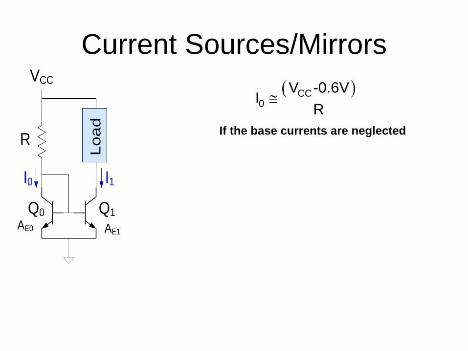
Current Sources/Mirrors
Q0
VCC
R
Q1
AE0 AE1
Lo
ad
I1I0
CC0
V -0.6VI
R
If the base currents are neglected

Current Sources/Mirrors
Q0
VCC
R
Q1
AE0 AE1
Lo
ad
I1I0
V1
CC0
V -0.6VI
R
If the base currents are neglected
BE0
t
V
V0 S E0I =J A e
BE1
t
V
V1 S E1I =J A e
since VBE1=VBE2
1E1
0E0
AI I
A
Behaves as a current sink ! So is ideal with this model !!
Note I1 is not a function of V1
0 6CCE1
E0
V . VA
A R
And does not require an additional dc voltage source !!!
Current Sources/Mirrors
Q0
VCC
R
Q1
AE0 AE1
I1I0 I1
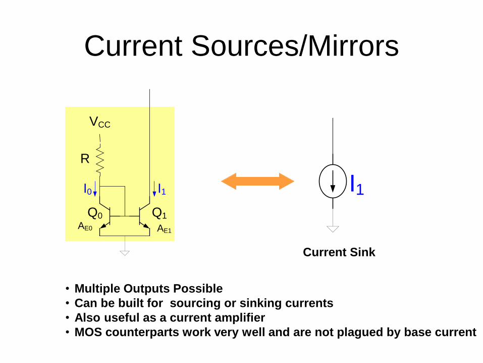
• Multiple Outputs Possible
• Can be built for sourcing or sinking currents
• Also useful as a current amplifier
• MOS counterparts work very well and are not plagued by base current
Current Sink
Current Sources/Mirrors
Q0
VCC
R
Q1
AE0 AE1
I1I0 I1
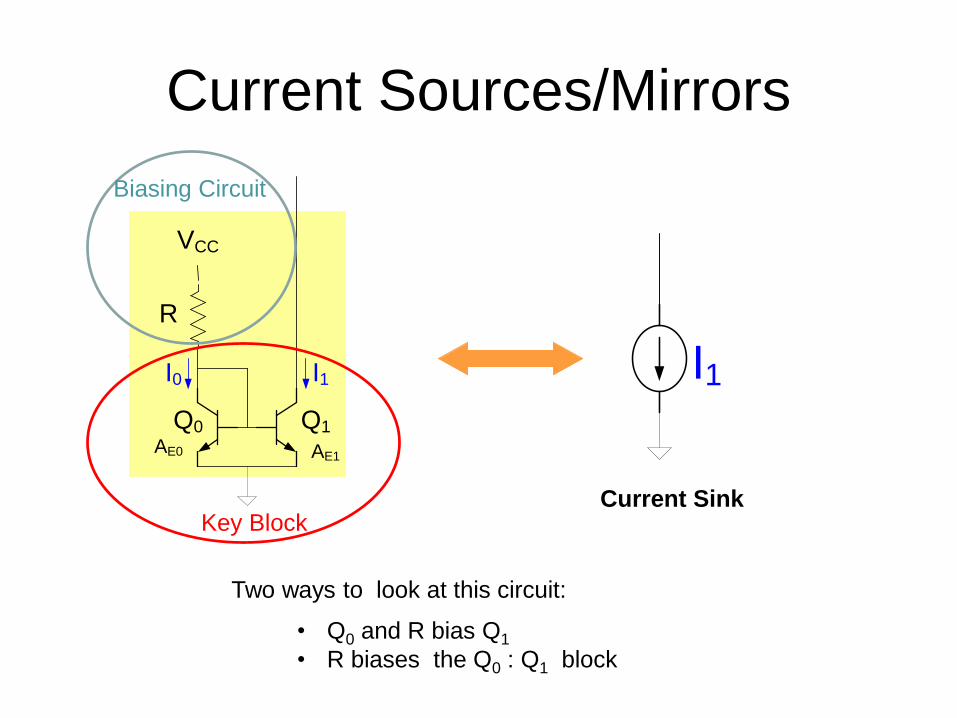
Current SinkKey Block
Biasing Circuit
Two ways to look at this circuit:
• Q0 and R bias Q1
• R biases the Q0 : Q1 block
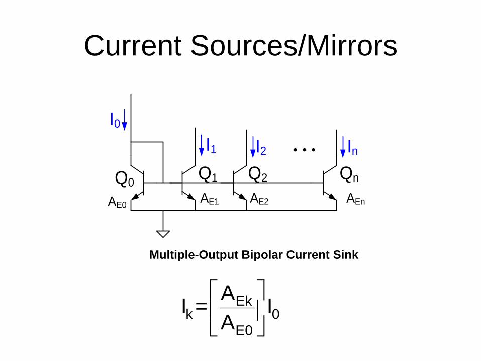
Current Sources/Mirrors
Q0Q1
AE1
I1
I0
Q2
I2
Qn
In
AE2 AEnAE0
Multiple-Output Bipolar Current Sink
Ekk 0
E0
AI = I
A

Current Sources/Mirrors
Multiple-Output Bipolar Current Source
Ekk 0
E0
AI = I
A
VDD
Q0 Q1 Q2 Qn
AE0 AE1 AE2 AEn
I1 I2 InI0
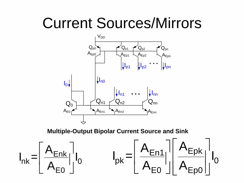
Current Sources/Mirrors
Multiple-Output Bipolar Current Source and Sink nkI =?
Q0Qn1
AE0 AEn1
In0I0
Qn2
In1
Qnn
Inn
AEn2
VDD
Qp0 Qp1 Qp2 Qpn
AEp0 AEp1 AEp2 AEpn
Ip1 Ip2 Ipn
AEnn
pkI =?
Current Sources/Mirrors
Multiple-Output Bipolar Current Source and Sink
Enknk 0
E0
AI = I
A
Q0Qn1
AE0 AEn1
In0I0
Qn2
In1
Qnn
Inn
AEn2
VDD
Qp0 Qp1 Qp2 Qpn
AEp0 AEp1 AEp2 AEpn
Ip1 Ip2 Ipn
AEnn
EpkEn1pk 0
E0 Ep0
AAI = I
A A

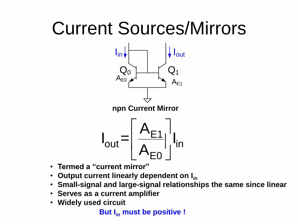
Current Sources/Mirrors
Q0 Q1
AE1
IoutIin
AE0
• Termed a “current mirror”
• Output current linearly dependent on Iin• Serves as a current amplifier
• Widely used circuit
npn Current Mirror
E1out in
E0
AI = I
A
But Iin and Iout must be positive !
Current Sources/Mirrors
Q0 Q1
AE1
IoutIin
AE0
• Termed a “current mirror”
• Output current linearly dependent on Iin• Small-signal and large-signal relationships the same since linear
• Serves as a current amplifier
• Widely used circuit
npn Current Mirror
E1out in
E0
AI = I
A
But Iin must be positive !

Current Sources/Mirrors
npn current mirror amplifier out=?i
Q0 Q1
AE0 AE1
iinIBS MIBSiout
E1
E0
AM=
A
OUT BS
in BS
+MIM
+I
i
i
OUT BS in BS+MI =M +Ii i
OUT BS in BS+M = IM +Ii i
OUT
in
=Mi
i
But IBS +iin >0 !

Current Sources/Mirrors
Amplifiers both positive and negative currents (provided iIN>-IBS )
npn current mirror amplifier
E1out in
E0
A=
A
i i
Q0 Q1
AE0 AE1
iinIBS MIBSiout
E1
E0
AM=
A
Current amplifiers are easy to build !!
Current gain can be accurately controlled with appropriate layout !!

Current Sources/Mirrors
n-channel Current Mirror
outI =?
M0 M1
W0,L0
Iout
Iin
W1,L1Q0
Q1
AE1
IOU T
I0
AE0
npn Current Mirror

Current Sources/Mirrors
n-channel Current Mirror
01out in
0 1
LWI = I
W L
M0 M1
W0,L0
Iout
Iin
W1,L1
2OX 0
in GS0 T00
μC WI = V -V
2L
2OX 1
out GS1 T11
μ C WI = V -V
2L
If process parameters are matched, it follows that
• Current mirror gain can be accurately controlled !
• Layout is important to get accurate gain (for both MOS and BJT)
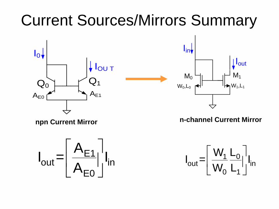
Current Sources/Mirrors Summary
n-channel Current Mirror
M0 M1
W0,L0
Iout
Iin
W1,L1Q0
Q1
AE1
IOU T
I0
AE0
npn Current Mirror
01out in
0 1
LWI = I
W L
E1out in
E0
AI = I
A

Layout of Current Mirrors
W2W1L1 L1
Example with M = 2
2 1
1 2
W LM=
W L
Standard layout
Gate area after fabrication depicted
2 2
2 22 1
1 2
W W L LM=
W W L L
2 22
2 21 1
1 1
2W W L LM=
W W L L
M1 M2
W1,L1
IoutIin
W2,L2
ΔW
ΔL
Layout of Current Mirrors
Example with M = 2
2 1
1 2
W LM=
W L
Standard layout
Better Layout
4 22
2 21 1
1 1
2W W L LM=
W W L L
2 22
2 21 1
1 1
2W W L LM=
W W L L
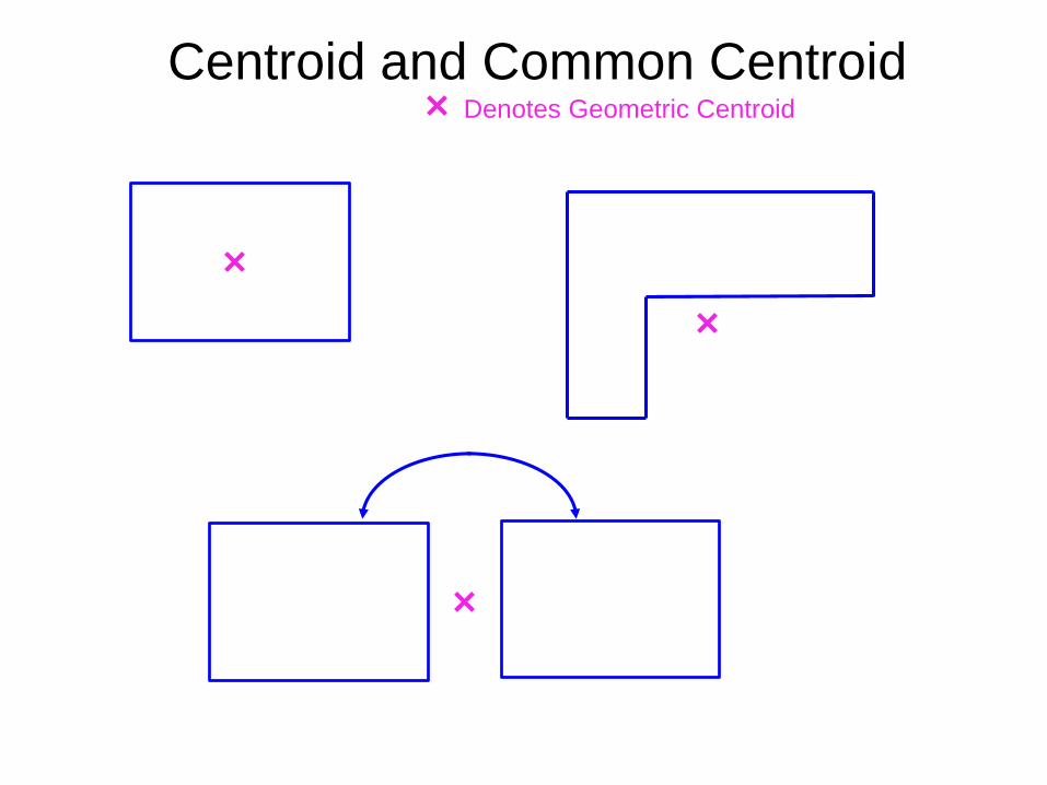
Centroid and Common CentroidDenotes Geometric Centroid
Centroid and Common Centroid
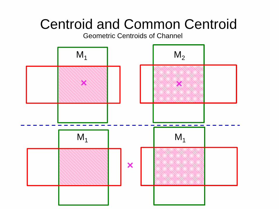
M1 M2
Geometric Centroids of Channel
M1 M1

Centroid and Common Centroid
M1 M1
M2M2
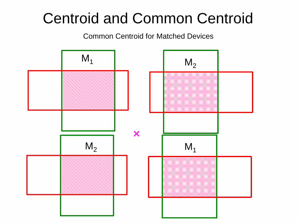
Centroid and Common Centroid
M1
M1
M2
M2
Common Centroid for Matched Devices

Centroid and Common Centroid
Common Centroid for Matched Devices
M1 M1M2 M2
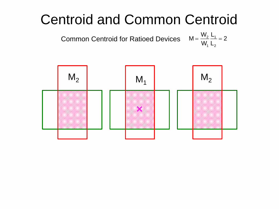
Centroid and Common Centroid
M2 M2M1
Common Centroid for Ratioed Devices 2 1
1 2
W LM 2
W L
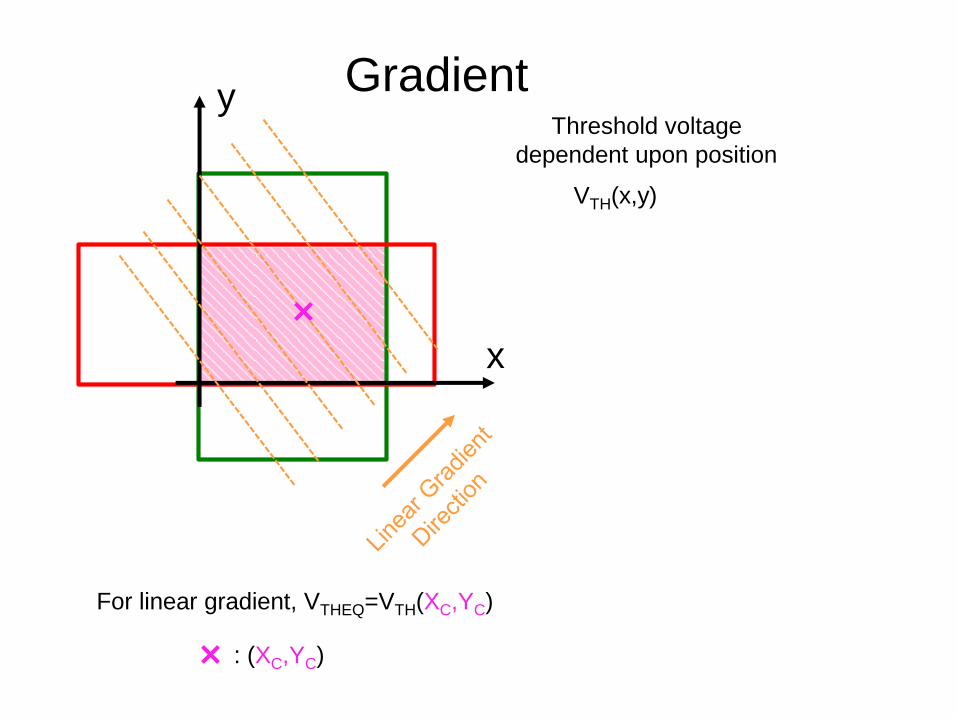
Gradient
x
y
VTH(x,y)
Threshold voltage
dependent upon position
For linear gradient, VTHEQ=VTH(XC,YC)
: (XC,YC)
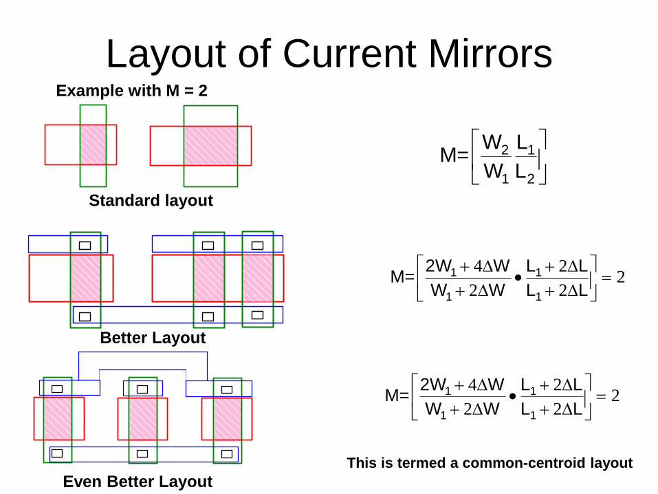
Layout of Current MirrorsExample with M = 2
2 1
1 2
W LM=
W L
Standard layout
Better Layout
4 22
2 21 1
1 1
2W W L LM=
W W L L
Even Better Layout
4 22
2 21 1
1 1
2W W L LM=
W W L L
This is termed a common-centroid layout

Stay Safe and Stay Healthy !

End of Lecture 33
Related Documents