EE 240B discussion 3 Eric Chang

Welcome message from author
This document is posted to help you gain knowledge. Please leave a comment to let me know what you think about it! Share it to your friends and learn new things together.
Transcript
EE240Bdiscussion3
EricChang

Outline
• HW1designsolution.• TransistorcharacterizationusingBAG.• Tipsoncascode design.
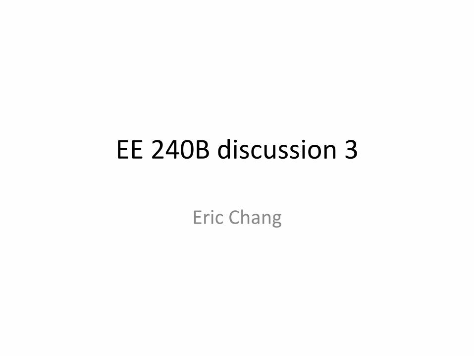
GeneralAmplifierDesignStrategy
• Gain/maximumBWindependentofsizeandloadcapacitance.
• BW/noiseimproveslinearitywithsize.• Strategy:designaunit-sizeamplifierfirstthatmeetsgainspecandhavesufficientmaximumBW.ThencomputeminimizesizethatmeetsBW/noiseconstraint.– Tominimizepower,pickthe“best”unit-sizeamplifier.

CSAmplifier
• Ignoreloadcapfirst,assume1finger.
• Whatistheminimumnumberofvariablesthatcompletelydeterminesamplifierperformance?

CSUnitAmplifierdesign
• Given𝑉"# and𝑉$#,allSSparametersandbiascurrentaredetermined.– LoadresistancealsodeterminedfromKCLand𝑉$$.
• Thus,given𝑉"# and𝑉$#,welookupSSparameters,and𝐴& = 𝑔)(𝑅,||𝑟/),𝑤)23 =[ 𝑅, 𝑟/ 𝐶66 78.
• If𝑤)23 > 𝑤:;,thenthesizeis𝑘 ==>/=@@ABCDAEA
78,and
biascurrentisjust𝑘 F 𝐼:H2I.

CSAmplifierflow
• Sweep𝑉"# and𝑉$#,foreachcombination,dothefollowing:– Compute𝐴& and𝑤)23.Ifeitherconstraintsfailed,goontonextcombination.
– Computeamplifiersize𝑘 andfinalbiascurrent.Thisisthesmallestcurrentwe’veseenrecordbiaspoint.
• Returnthebestoperatingpoint.

BAG:UniversalVerificationFramework
• Withschematicgenerators,itisnowpossibletodeveloptestbenches thatworkwitharbitrarycircuits.
• Complexmeasurementproceduresnowonlyneedtobeprogrammedonce,thencanbere-usedeverywhere.
• Transistorcharacterizationisthefirsttestbenchdevelopedinthisframework.

BAG’stransistorchar.algorithm1. Determinestherangeof𝑉"# thatcorrespondstoarange
ofuser-specifiedcurrentdensity(uA/finger)a) Designergenerallyhaveabetterideaontheboundsofcurrent
densityinsteadof𝑉"# rangeb) Thisgivesusfiner𝑉"#stepsizeforthesamenumberofpoints.
2. SimulateYparameters(atagivenfrequency)acrossbiaspointsandextractsmall-signalparameters.
3. (Optional)Simulatenoise,thencalculate“effective𝛾”fromagivenintegrationinterval.a) Calculates𝛾 from𝑔) andtotalintegratednoiseassuming
whitenoisespectrum.b) worksbestfornarrow-bandnoisecharacterization(orwhen
flickernoiseisnotdominant).4. Resultssavetoadatabaseandavailableasinterpolated
functions.

Transistorcharacterizationspecificationfile
• Characterizationsettingsspecifiedinspecs_mos_char/*.yaml.
• dut_lib/dut_cell definesthetransistorbeingcharacterized.
• schematic_params sectiondefinestheschematicparametersofthetransistor.
• measurementssectionscontainscharacterizationoptions.
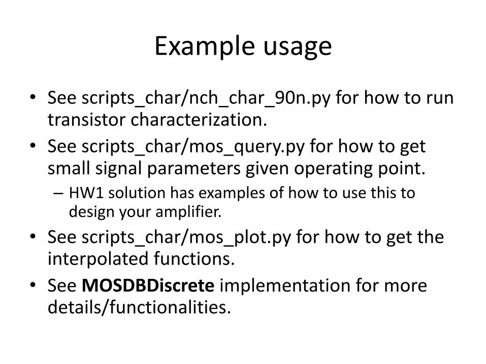
Exampleusage
• Seescripts_char/nch_char_90n.pyforhowtoruntransistorcharacterization.
• Seescripts_char/mos_query.py forhowtogetsmallsignalparametersgivenoperatingpoint.– HW1solutionhasexamplesofhowtousethistodesignyouramplifier.
• Seescripts_char/mos_plot.py forhowtogettheinterpolatedfunctions.
• SeeMOSDBDiscrete implementationformoredetails/functionalities.

Cascode designnotes• Whyiscascode designhard?
– Manypossiblecombinationofsizes/biasvoltages.
• Howyougeneratethebiasvoltagecanreducedegreesoffreedom.
• “Lazy”bias:justtietoVDD/VSS.– Onlypossiblewayinlow-voltage
processes.– Largeprocess/supplyvariations.
• Cascode currentmirrorbias.– Morestableacrossvariations.– Biasvoltagesfunctionofbiasnetwork
->simplifiesdesign.• Forhomework,yougetidealvoltage
source.– Lesscircuitstobuild,butharderto
design.

Cascode design:blindsweeping• Vb constant->drawablackboxandthinkofitasone“compositetransistor”.– AslongasthepoleatVm isnegligible,whichistrueformostopen-loopapplications.
• Canusethesametransistorcharacterizationroutinetocharacterizecascode transistors.– Havetosweep5+variables,butgivesthemostaccurate/optimaldesign.
– Seench_char_cas.py andmos_plot_cas.py forexamplesofhowtocharacterizeanduseMOSDBDiscrete withcascodetransistors.

Cascodedesign:𝑉∗/𝐴&M based• Notethat𝑉∗ = 2𝐼:H2I/𝑔) implies𝑉∗
ofthecompositetransistor=𝑉∗ ofthebottomtransistor.
• Specify𝑉:/O∗ ,𝑉O/P∗ /𝑉:/O∗ ,and𝐴&M,)HR ofbothtransistors.– 𝐴&M,)HR ensuresthatbothtransistorsare
in“saturation”,andknowingratioof𝑉∗makesdesigningbiasnetworkeasy.
• Firstfindlowest𝑉) suchthat𝑉:/O∗ and𝐴&M,)HR specscanbemet.– Thisgiveslargestheadroomfortop
transistor.• Thenfind𝑉S2I from𝑉O/P∗ .Checkthat
cascode transistormeet𝐴&M,)HR spec.– Ifnotthenthespecsareimpossibleto
meet.
Related Documents