1 Tutorial 1 Introduction to EDK 10.1 and the Digilent V2Pro Board -Introduction This lab will be an introduction to design techniques for EDK using the Digilent V2Pro board. It will explain the basics of building a project with the wizard and then expanding the project to include a hello world option. It will be necessary to have a null-modem cable to communicate between the Hyper Terminal on the PC and the V2Pro FPGA platform. The project is completed using EDK 10.1, Windows Vista and the V2Pro board. -Objective The objective is to understand the basics of the EDK software. This will be accomplished through the implementation of a UART in an FPGA. The circuit will be designed in such a way that the phrase “hello world” will be displayed to a HyperTerminal. -Application This document is used by students, who are learning FPGA design using EDK. -RS-232 Serial Interface 1. Characteristics Uses a 9 pin connector DB-9 (older PCs use 25 pin DB-25 connectors and newer laptops do not have serial port anymore, so a USB to serial converter is required). Allows bidirectional full-duplex communication (the PC can send and receive data at the same time). Can communicate at a maximum speed of roughly 10KBytes/s. 2. DB-9 Connector DB-9 connector (male) appears as shown in Figure 1. Figure 1: DB-9 Connector

Welcome message from author
This document is posted to help you gain knowledge. Please leave a comment to let me know what you think about it! Share it to your friends and learn new things together.
Transcript

1
Tutorial 1
Introduction to EDK 10.1 and the Digilent V2Pro Board
-Introduction
This lab will be an introduction to design techniques for EDK using the Digilent V2Pro
board. It will explain the basics of building a project with the wizard and then expanding
the project to include a hello world option. It will be necessary to have a null-modem
cable to communicate between the Hyper Terminal on the PC and the V2Pro FPGA
platform.
The project is completed using EDK 10.1, Windows Vista and the V2Pro board.
-Objective
The objective is to understand the basics of the EDK software. This will be accomplished
through the implementation of a UART in an FPGA. The circuit will be designed in such
a way that the phrase “hello world” will be displayed to a HyperTerminal.
-Application
This document is used by students, who are learning FPGA design using EDK.
-RS-232 Serial Interface
1. Characteristics
Uses a 9 pin connector DB-9 (older PCs use 25 pin DB-25 connectors and newer
laptops do not have serial port anymore, so a USB to serial converter is required).
Allows bidirectional full-duplex communication (the PC can send and receive
data at the same time).
Can communicate at a maximum speed of roughly 10KBytes/s.
2. DB-9 Connector
DB-9 connector (male) appears as shown in Figure 1.
Figure 1: DB-9 Connector

2
The pin numbering on the connector is as follows:
Figure 2: Pin Numbering (male connector)
Figure 3: Pin Numbering (female connector)
Pin Description of RS-232 male connector:
Pin
No.
Name Dir Notes/Description
1 DCD IN Data Carrier Detect. Raised by DCE when modem synchronized.
2 RD IN Receive Data (RD, Rx). Arriving data from DCE.
3 TD OUT Transmit Data (TD, Tx). Sending data from DTE.
4 DTR OUT Data Terminal Ready. Raised by DTE when powered on. In auto-
answer mode raised only when RI arrives from DCE.
5 GND - Ground
6 DSR IN Data Set Ready. Raised by DCE to indicate ready.
7 RTS OUT Request To Send. Raised by DTE when it wishes to send. Expects
CTS from DCE.
8 CTS IN Clear To Send. Raised by DCE in response to RTS from DTE.
9 RI IN Ring Indicator. Set when incoming ring detected - used for auto-
answer application. DTE raised DTR to answer.
Table 1: Pin Description (male connector)

3
The three important ones among the 9 pins are:
pin 2: RD (receive data).
pin 3: TD (transmit data).
pin 5: GND (ground).
Using just 3 wires, one can send and receive data.
3. Serial Communication
Data is sent one bit at a time. One wire is used for each direction. Since computers
usually need at least several bits of data, the data is serialized before being sent. Data is
commonly sent by chunks of 8 bits. The LSB (data bit 0) is sent first, the MSB (bit 7) is
sent last.
4. Asynchronous Communication
This interface uses an asynchronous protocol which means that no clock signal is
transmitted along with data. The receiver has to have a way to time itself to the incoming
data bits.
In the case of RS-232, it is done in the following way:
1. Both side of the cable agree in advance on the communication parameters
(parameters shown in Figure 4). It is done manually before communication starts
(which will be explained later).
Figure 4: Serial Communication Parameters
2. The transmitter sends a "1" when the line is idle.
3. The transmitter sends a "start" (a "0") before each byte is transmitted, so that the
receiver can understand that data is coming.
4. After the "start", data comes in with the agreed speed and format, so the receiver
can interpret it.
5. The transmitter sends a "stop" (a "1") after each data byte.

4
For example, a 0x55 byte when transmitted appears in the following way:
Figure 5: 0x55 Byte Transmission
Byte 0x55 is 01010101 in binary.
But since it is transmitted LSB (bit-0) first, the line toggles like that: 1-0-1-0-1-0-1-0.
Another example:
Figure 6: 0xC4 Byte Transmission
Here the data is 0xC4, which is difficult to interpret. It an illustration to show how
important it is for the receiver to know at which speed the data is sent.
5. Operation Speed
The speed is specified in baud, i.e. how many bits-per-seconds can be sent. For example,
1000 bauds would mean 1000 bits-per-seconds, or that each bit lasts one millisecond.
Common implementations of the RS-232 interface (like the one used in PCs) do not
allow just any speed to be used. One has to settle to some "standard" speed.
Common values are:
1200 bauds.
9600 bauds.
38400 bauds.
115200 bauds.
At 115200 bauds, each bit lasts (1/115200) = 8.7µs. If one transmits 8-bit data, it lasts for
8 x 8.7µs = 69µs. But each byte requires an extra start and stop bit, so one actually needs
10 x 8.7µs = 87µs. That translates to a maximum speed of 11.5 KBytes per second.
At 115200 bauds, some PCs with faulty chips require a "longer" stop bit (1.5 or 2 bits
long) which makes the maximum speed drop to around 10.5KBytes per second.
6. Physical Layer
The signals on the wires use a positive/negative voltage scheme.
"1" is sent using -10V (or between -5V and -15V).
"0" is sent using +10V (or between 5V and 15V).
So an idle line carries something like -10V.

5
-Initial Set-up
Figure 7: USB-to_Serial Converter
1. Connect the serial port available on the FPGA board to the USB port available on the
laptop/PC using a USB-to-Serial converter as shown.
Note: Download the USB-to-Serial converter driver from the manufacturers website.
Figure 8: USB Connection
6
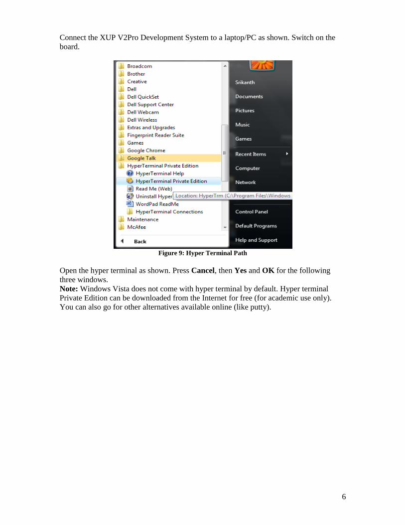
Connect the XUP V2Pro Development System to a laptop/PC as shown. Switch on the
board.
Figure 9: Hyper Terminal Path
Open the hyper terminal as shown. Press Cancel, then Yes and OK for the following
three windows.
Note: Windows Vista does not come with hyper terminal by default. Hyper terminal
Private Edition can be downloaded from the Internet for free (for academic use only).
You can also go for other alternatives available online (like putty).

7
Figure 10: Hyper Terminal
Once this window shows up give an appropriate name and press OK. Again press
Cancel, then Yes and OK for the following three windows.
Figure 11: Com Port Selection
Then the following window will show up. Select the appropriate Com Port and press OK.
If you are unsure about which COM Port you are using, you can see by going to the
Device Manager under the hardware tab. To get there, go to control panel and then
system.

8
Figure 12: Hyper Terminal Settings
The following window will show up. Make the port settings as shown or set the baud rate
to a desired rate depending on the design parameters. As the baud rate in the present
design is configured for 9600 baud, the following settings are been chosen.
Figure 13: New Hyper Terminal Window
Once the port settings are made press OK and the terminal will show up.

9
-Implementation
1. Open Xilinx Platform Studio by selecting it from the start menu.
Figure 14: XPS Project Selection
2. The Xilinx Platform Studio, or XPS, Base System Builder will launch. For the
purposes of this tutorial, it is important to use the Wizard. Select the top option.
Figure 15: Project Directory and Repository Selection
3. Choose a directory for the sample project. Avoid directory names with spaces in them.
Since V2Pro board is not a default development board available in the base system
builder we need to point the User Peripheral Repository Directory to the EDK XUP-V2P
support files by selecting Set Project Peripheral Repositories and browse to the
location where you saved the support files.
Note: These files will be provided to you along with this tutorial or can be downloaded at
http://digilentinc.com/Data/Products/XUPV2P/EDK-XUP-V2ProPack.zip

10
Figure 16: BSB Screen
4. Choose to create a new design. The BSB (Base System Builder) allows the user to be
able to open a new design or to import the BSB settings from a previous project. Click
Next and it will show the Base System Builder window.

11
Figure 17: Board Selection
5. The board selection will be the Xilinx V2Pro. There is only one revision of this
board so this selection is easy. Click Next.
Note: The reason you are able to view this board in drop down list is because you added
the support files related to this board in step 3.
12
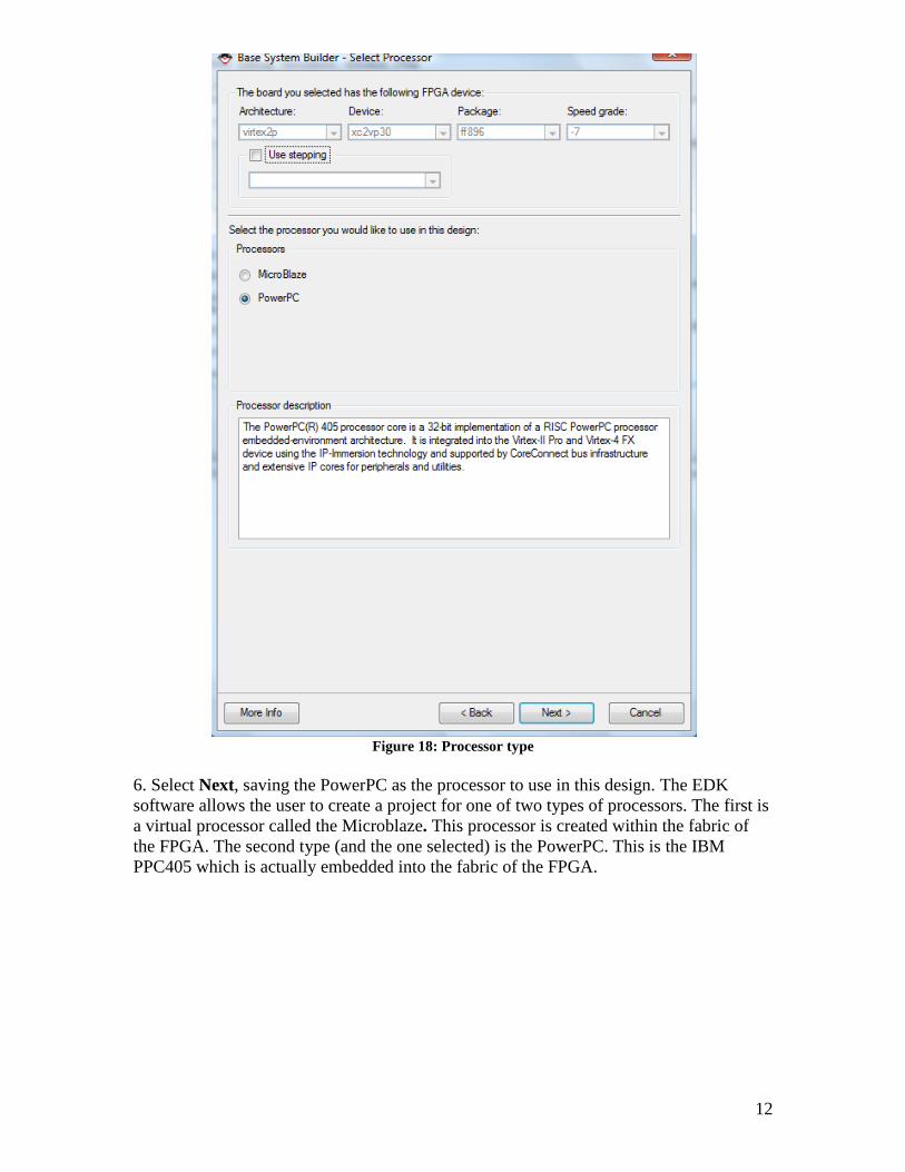
Figure 18: Processor type
6. Select Next, saving the PowerPC as the processor to use in this design. The EDK
software allows the user to create a project for one of two types of processors. The first is
a virtual processor called the Microblaze. This processor is created within the fabric of
the FPGA. The second type (and the one selected) is the PowerPC. This is the IBM
PPC405 which is actually embedded into the fabric of the FPGA.

13
Figure 19: Basic Selections
7. Select Next, saving the default settings. This is a menu specifically designed to
configure the PowerPC. If there were a desire to change the clock frequencies then they
could be done here. By clicking on the “More Info” button, more information on the
changeable values can be obtained.

14
Figure 20: Screen 1 of 2 for Interfaces
8. This is the first of two screens for choosing input and output interfaces. As shown in
the screen above, select the XPS UARTLITE. Deselect all other options, and then click
Next. This project will only have two items associated with the Processor Local Bus or
PLB. The two items used will be the UART and the BRAM (Block Ram).

15
Figure 21: Screen 2 of 2 for Interfaces
9. This is the last screen for adding interfaces. For this tutorial, deselect all the options,
and then click Next.

16
Figure 22: Internal Peripherals
10. Choose 64KB of BRAM, and then select Next.

17
Figure 23: Software Setup
11. This is the Software Setup screen. It is where choices are made as to which items will
be used by STDIN and STDOUT. In the case of this tutorial, HyperTerminal will use the
RS232_Uart for both sets of communications. Since the project is using only one type of
memory, the section is easy. For the purposes of this tutorial, deselect Memory test and
Peripheral selftest. Click Next.

18
Figure 24: Address Maps
12. The address maps displayed above show that there are two items assigned to the PLB:
BRAM and UART. The BRAM has FFFF or 64K of memory assigned. Select Generate.
19
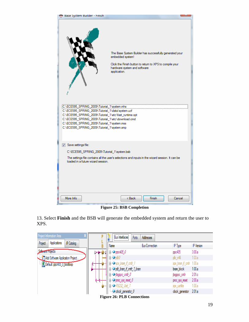
Figure 25: BSB Completion
13. Select Finish and the BSB will generate the embedded system and return the user to
XPS.
Figure 26: PLB Connections
20
14. The PLB connections are now shown. The user can see where the PLB makes
connections with the BRAM and the UART. Figure 15 shows that there is only one
software project associated so far, Default:ppc405_0_bootloop.
Default:ppc405_0_bootloop contains the MicroBlaze™ or PowerPC™ bootloop (Step
17) executables that cause the MicroBlaze or PowerPC embedded processors to loop at
the reset vector. This guarantees that the embedded processor stays in a known goodstate.
XPS creates the bootloops automatically for each new project. To make use of the
bootloop, mark the bootloop application in your XPS project for initialization of Block
RAMs (BRAMs). Ensure that multiple applications are not initialized into the BRAMs at
the same time.
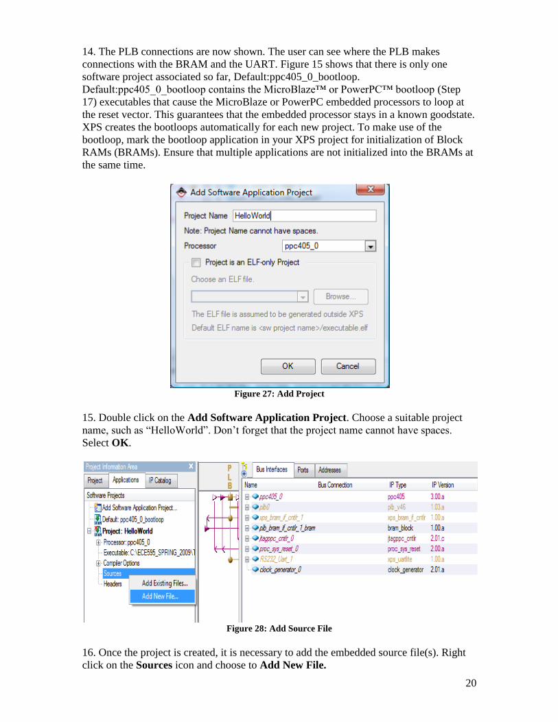
Figure 27: Add Project
15. Double click on the Add Software Application Project. Choose a suitable project
name, such as “HelloWorld”. Don’t forget that the project name cannot have spaces.
Select OK.
Figure 28: Add Source File
16. Once the project is created, it is necessary to add the embedded source file(s). Right
click on the Sources icon and choose to Add New File.

21
Figure 29: Hello World
17. For clarity and easy of file management, it is recommended that you create a
directory and store all your source files in it. For this example, a new directory called
SourcesC was created and the source file HWorld.c was created and stored there. This
will be an empty file.
Figure 30: HelloWorld.c
18. Expand Sources, and then double click on the HWorld.c file to open it. All that is
needed in this source file is the seven lines shown above. This will print to the STDIO
(UART) the phrase “hello world”.

22
Figure 31: Linker Script
19. Right-click on the Project: HelloWorld and select Generate Linker Script.
Figure 32: Memory Assignments
20. Click OK.
Note:
1) The default linker script uses a fixed start address of 0xFFFF0000 for PowerPC.
Modify the start address to reflect the address corresponding to the memory defined in
your hardware system. Default linker scripts assume a contiguous memory starting from
the address defined as the start address. If the application cannot fit into this contiguous
region, or if the application needs to be split across different memories in the system,
then a custom linker script is needed. Run the Generate Linker Script command to create
a custom linker script for the application.
2) If Output Linker Script default path says anything more than file name (example:
HelloWorld/HelloWorld_linker_script.ld), change it just file as shown in the above
figure.

23
Figure 33: Initialize BRAM
21. It is necessary to initialize the BRAM with the hello world project. Right-click on
Default:ppc405_0_bootloop and deselect the Mark to Initialize BRAMs option.
Choose the Mark to Initialize BRAMs option for Project: HelloWorld. There should
no longer be a red “x” on the Project: HelloWorld icon.
Figure 34: Update Bitstream
22. Under Device Configuration, choose Update Bitstream.
Note: If the following error occurs continue else skip to step 30.
ERROR: ConstraintSystem:8 - The file 'system.ucf' could not be opened for reading.
24
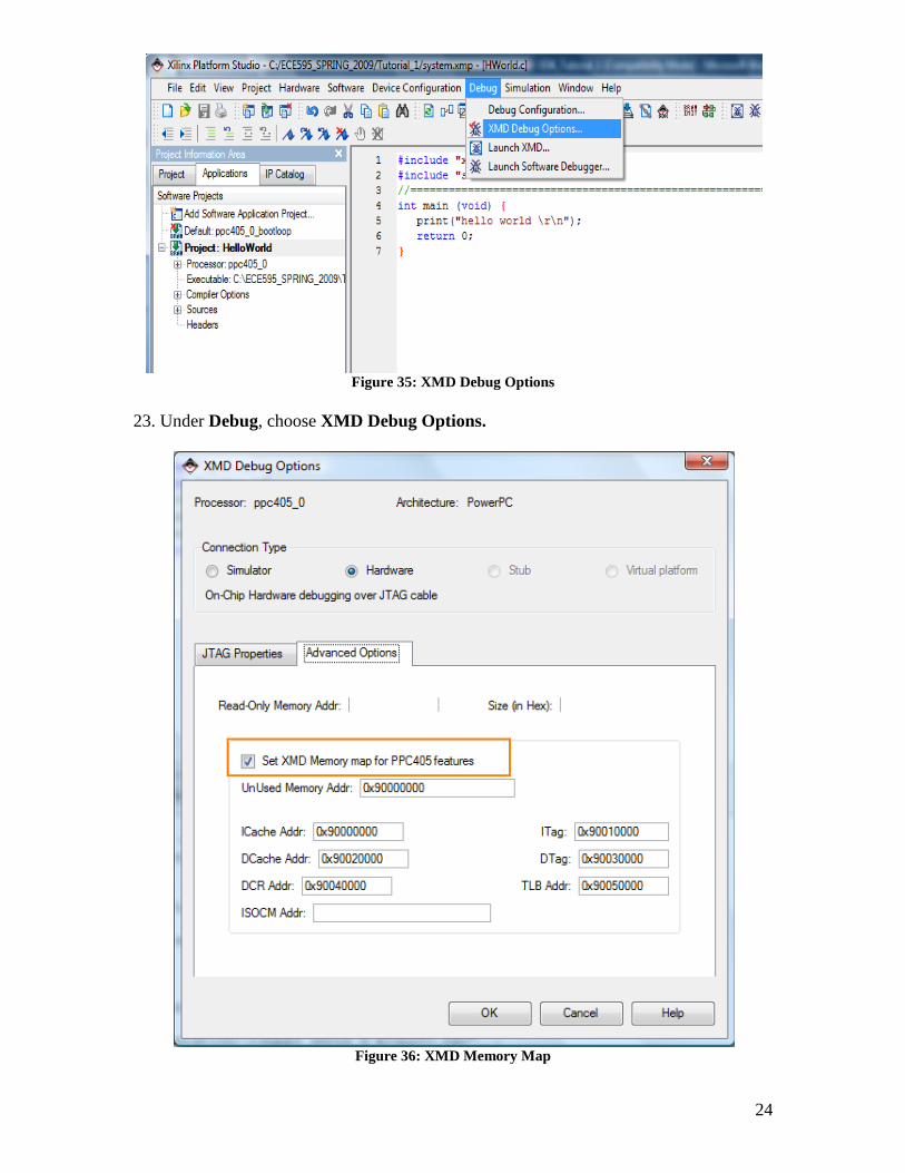
Figure 35: XMD Debug Options
23. Under Debug, choose XMD Debug Options.
Figure 36: XMD Memory Map

25
24. Under Advanced Options, select Set XMD Memory map for PPC405 features.
Figure 37: xbash
25. Under Debug, choose Launch XMD.
Figure 38: Modify Permissions
26. Change the permission of 'data' directory as follows: chmod 777 data. If it says
permission denied as shown above continue else skip to step 29.

26
Figure 39: System properties
27. Right-click the My Computer icon and select Properties. Select the Advanced tab.
Figure 40: Environment variables

27
28. Select the Environment Variables button. Under System variables, select the New
button. For the variable name, enter CYGWIN. For the variable value, enter "nontsec".
Select the OK button three times. If XPS was open, restart XPS so that it will recognize
the new environment variable.
Figure 41: Permissions Modification
29. Repeat step 26. Go into 'data' directory and change the permission of system.ucf file
as shown above by using command: chmod 777 system.ucf
Figure 42: Download Bitstream
30. If the entire software application fits on FPGA block RAM (BRAM) blocks, the
system can be initialized by updating the hardware bitstream with the BRAM
initialization data. This updated bitstream can then be downloaded to the FPGA. Under
Device Configuration, choose Download Bitstream. The bitstream is initialized with the
executable. In the XPS (non-submodule) flow, this will result in the generation of the
<project>/implementation/download.bit bitstream filecontaining both hardware and
software.

28
Figure 43: Output
31. Once the project has completed and downloaded, the HyperTerminal will display
hello world.
-Author Bio
Name: Vallabh Srikanth Devarapalli
Graduate student at UNM in ECE department.
E-mail: [email protected].
Related Documents