ELECTRONIC DEVICES AND CIRCUITS BRIEF NOTES UNIT – I :: ELECTRON DYNAMICS: CRO 19 31 1.602 10 , 9.1 10 e C m kg − − = × = × , ‘F’ force on electron in uniform electric field ‘E’ F=eE; acceleration eE a m = If electron with velocity ' ' v moves in field ' ' E making an angle ' ' θ can be resolved to sin , cos v v θ θ . Effect of agnetic Field ‘!’ on Electron. "hen ! # $ are %er%endicular %ath is circular 2 ; ' ' mv m r Period t Be Be π = = "hen slant with ' ' θ %ath is & 'elical. E$()*I+- +F /* E0E*/+-*)*I 1EF0E*I+ -E-I*I2I*3 2 e a lL S dV = )4E*I 1EF0E*I+ -E-I*I2I*3 2 m a e S lL mV = 2elocity due to voltage 2, 2eV v m = "hen E and ! are %er%endicular and initial velocity of electron is 5ero, the %ath is ycloidal in %lane %er%endicular to ! # E. 1iameter of ycloid=6$, where u Q ω = , E u B = , Be m ω = . UNIT – II :: SEMICONDUCTOR JUNCTION , i e S G have 7 electrons in covalent bands. 2alency of 7. 1o%ing with trivalent elements makes ' ' p , 8entavalent elements makes ' ' n semiconductor. onducti vi ty ( ) n p e n p σ µ µ = + where , n p are concen trations of 1o%ants. & n p µ µ are mobility’s of electron and hole res%ectively. - 1 - 1iode e9uation 1 d T V nV d s I I e = − ÷

Welcome message from author
This document is posted to help you gain knowledge. Please leave a comment to let me know what you think about it! Share it to your friends and learn new things together.
Transcript

8/13/2019 Edc Brief Notes
http://slidepdf.com/reader/full/edc-brief-notes 1/13
ELECTRONIC DEVICES AND CIRCUITS
BRIEF NOTES
UNIT – I :: ELECTRON DYNAMICS: CRO
19 311.602 10 , 9.1 10e C m kg − −= × = × , ‘F’ force on electron in uniform electric field ‘E’
F=eE; accelerationeE
am
=
If electron with velocity ' 'v moves in field ' ' E making an angle ' 'θ can be
resolved to sin , cosv vθ θ .
Effect of agnetic Field ‘!’ on Electron.
"hen ! # $ are %er%endicular %ath is circular2
; ' 'mv m
r Period t Be Be
π = =
"hen slant with ' 'θ %ath is & 'elical.
E$()*I+- +F /*
E0E*/+-*)*I 1EF0E*I+ -E-I*I2I*32
e
a
lLS
dV =
)4E*I 1EF0E*I+ -E-I*I2I*32
m
a
eS lL
mV =
2elocity due to voltage 2,2eV
vm
=
"hen E and ! are %er%endicular and initial velocity of electron is 5ero, the %ath is
ycloidal in %lane %er%endicular to ! # E. 1iameter of ycloid=6$, whereu
Qω
= ,
E u
B= ,
Be
mω = .
UNIT – II :: SEMICONDUCTOR JUNCTION
,i e
S G have 7 electrons in covalent bands. 2alency of 7. 1o%ing with trivalent
elements makes ' ' p , 8entavalent elements makes ' 'n semiconductor.
onductivity ( )n pe n pσ µ µ = + where ,n p are concentrations of 1o%ants.
&n p
µ µ are mobility’s of electron and hole res%ectively.
- 1 -
1iode e9uation
1d
T
V nV
d s I I e
= − ÷
8/13/2019 Edc Brief Notes
http://slidepdf.com/reader/full/edc-brief-notes 2/13
2; lnd T A P
d o
d i
V V N N kT r V
I I q n
∆= = = ÷∆
0 190 273; 1.602 10T C q C −= + = ×
1iode dro% changes0@ 2.2 /mv C , 0eakage current s
I doubles on 010 C
1iffusion ca%acitance is d
dqc
dv= of forward biased diode it is I µ
*ransition ca%acitance T C is ca%acitance of reverse biased diode
nV −µ 1 12 3
n to=
/E*IFIE/-
+8)/I-I+
'" F" * F" !/
C V m
V π
2m
V π
2m
V π
rmsV
2m
V 2
mV
2m
V
- 2 -
;T
kT V
q= := !olt5man onstant

8/13/2019 Edc Brief Notes
http://slidepdf.com/reader/full/edc-brief-notes 3/13
γ
/i%%le factor 1.21 0.482 0.482
η
/ectification efficiency40.6% 81% 81%
PIV 8eak Inverse 2oltage m
V 6 mV
mV
UNIT – III :: FILTERS
'armonic om%onents in F" +ut%ut, 0
2 4 1 1cos 2 cos 4 .....
3 15
mV
v !t !t
π π
= − + +
- 3 -
a%acitance In%ut Filter,
Inductor In%ut Filter,ritical inductance is that value at whichdiode conducts continuously, in or half cycle.
0 FI0*E/,
2
2
12 LC γ
ω = or
1.2, 50 , , . "or #$ L in # C in %
LC µ
FI0*E/,
/ FI0*E/,
0 0)11E/,1 2
1 2
2. . .....
3
n
n
cc c
L L L
& & &
& & & γ =
8/13/2019 Edc Brief Notes
http://slidepdf.com/reader/full/edc-brief-notes 4/13
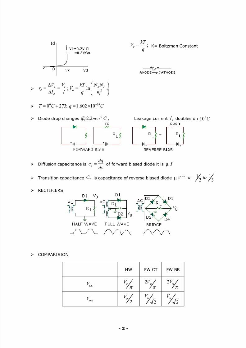
EE/ 1I+1E
EE/ /E4(0)*+/
;i $ s i $
s
V V I V V
'
−= >>
$
$ $
V r
I ∆= ∆
*(E0 1I+1E
onducts in , " r
( (, $uantum mechanical tunneling in region a<<b<c.
<ve resistance b<c, normal diode c<d.
p I = %eak current, v
I = valley current; pv =%eak voltage > ?@ m2, v
v =valley voltage
.A@ 2. 'eavy 1o%ing, arrow Bunction , (sed for switching # 'F oscillators.
2)/)*+/ 1I+1E
(sed in reverse bias # as tuning variable ca%acitance.
( )
T n
T '
) C
V V =
+; n=.A for diffusion, n=.@ for alloy Cunction,
1
oT n
'
T
C C
V V
= + ÷
25
BC C
is figure of merit, -elf resonance 12
o
S T
" L C π
=
- 4 -
F"1 !ias ormal1iode .D 2 1ro%
/everse !ias

8/13/2019 Edc Brief Notes
http://slidepdf.com/reader/full/edc-brief-notes 5/13
8'+*+ 1I+1E-
1iode used in reverse bias for light detection.
1ifferent materials have individual %eak res%onse to a range of wave lengths.
UNIT - IV
!B*, !i%olar Bunction *ransistor has 6 Bunctions !E, !
om%onents of current are ,nE pE
I I at EB Cunction wherenE nE
nE pE E
I I
I I I γ = =
+
γ = Emitter efficiency,* nc
nE
I
I β = trans%ortation factor.
/ ; / BE " ( BC r (= =
- 5 -
e ( c I I I = +
;c c
e (
I I
I I α β = =
1o%ing Emitter 'ighest
!ase 0owest
e c ( I I I > >

8/13/2019 Edc Brief Notes
http://slidepdf.com/reader/full/edc-brief-notes 6/13
0eakage currents , ,CB* CE* EB*
I I I
( )1CE* CB*
I I β = +
A onfigurations are used on !B*, E, ! #
ommon Emitter, 2I characteristics
0; ce BE
i ie e ce
B c
V V ' + r r r
I I β
∆∆= = = = =
∆ ∆
AC Equiv!"#$ Ci%&ui$
++ !)-E 2I ')/)*E/I-*I-
- ' -
I#(u$ C)%&$"%i*$i&* Ci%&ui$ Ou$(u$ C)%&$"%i*$i&*
CE
C V
B
I
I β =

8/13/2019 Edc Brief Notes
http://slidepdf.com/reader/full/edc-brief-notes 7/13
;
1
C
E
I
I
β α α
β
= =
+
; ;V CB
C c( EBi( e "( c(
E e c
I V V + r + r
I I I
∆∆= = = =
∆ ∆
UNIT - V
h< %arameters originate from e9uations of am%lifier
2 2 0 2,
i i i r " iv + i + v i + i + v= + = +
&i i
v i are in%ut voltage and current
2 2&v i are out%ut voltage and current
i+ → in%ut im%edance , ,
ie i( ic+ + + ( ), , 1
e e er r r β β +
" + → current gain , ,
"e "( "c+ + + ( ), , 1β α β +
r + → reverse voltage transfer , ,
re r( rc+ + +
o+ → out%ut admittance , ,
oe o( oc+ + +
FIE01 EFFE* */)-I-*+/, FE* is (ni%olar 1evice
- + -
COM,ARISON
!E !
-)*(/)*I+ fb fb
)*I2E fb rb
(* +FF rb rb
)80IFIE/ +8)/I-+
! E F
i ' 0+" E1 'I4'
I A
I A β 1β +
V A 'igh 'igh GH
o ' 'igh 'igh low
AC Equiv!"#$ Ci%&ui$

8/13/2019 Edc Brief Notes
http://slidepdf.com/reader/full/edc-brief-notes 8/13
C#*$%u&$i# #-C)##"! (-C)##"!
-=-ource, 4=4ate, 1=1rain
4- Bunction in /everse !ias )lways
gsV ontrols 4ate "idth
2I ')/)*E/-*I-
T%#*."% C)%&$"%i*$i&* Ci%&ui$ F%/%0 C)%&$"%i*$i&*
-hockley E9uation
2
1 gs
d dss
p
V I I
V
= − ÷ ÷
, 0
1 gs
m m
p
V g g
V
= − ÷ ÷
+-FE* etal +ide -emiconductor FE*, I4FE*
D"(!"$i# T(" M*."$ S!* E#)#&""#$ M*."$
1e%letion *y%e +-FE* can work width 0 gs
V > and 0 gs
V <
T%#*."% F%/%0
C)%&$"%i*$i&* C)%&$"%i*$i&*
- -
MOSFET J,ET
'igh1010
i ' = 810−
050 ' k = Ω 1m≥ Ω
1e%letionEnhancement ode
1e%letionode
1elicate /ugged
8/13/2019 Edc Brief Notes
http://slidepdf.com/reader/full/edc-brief-notes 9/13
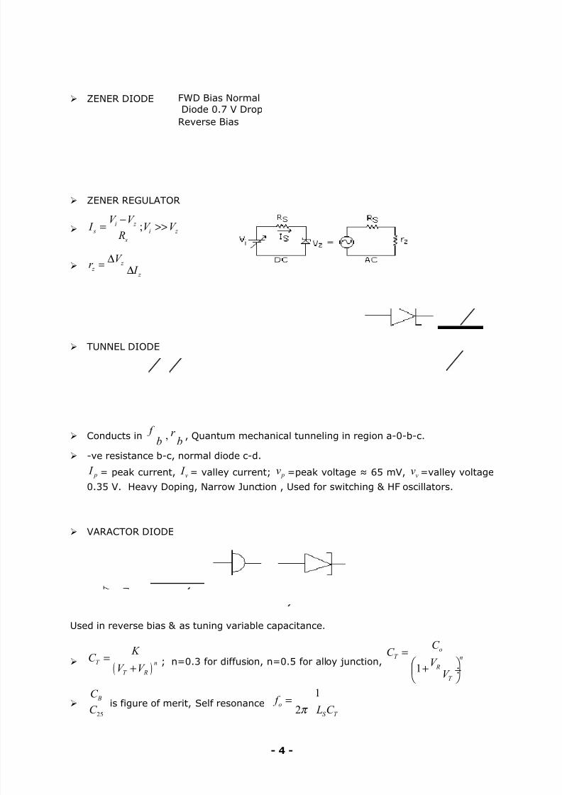
Enhancement +-FE* o%erates with, gs t V V > , t V T+res+old Voltage=
F%/%0 C)%&$"%i*$i&* T%#*."% C)%&$"%i*$i&*
UNIT – VI :: BIASIN i# BJT 6 JFET
Fiing +%erating 8oint $ is biasing
Fied !ias Emitter -tabili5ed Feedback !ias
CC B B BE V I ' V = + Fied !ias ( )1
CC C B B B BE V ' I I ' V β = + + +
( )1 ReCC B B BE
V I ' V β = + + +
- 7 -
,%ET I Ta(le
gsV
I
SS I
.A P V 2
SS I
.@ P V
4 SS
I
P V
COM,ARISIONS
BJT FET
urrent controlled 2oltage controlled
'igh gain ed gain
!i%olar (ni%olar
*em% sensitive 0ittle effect of *
'igh 4!"8 0ow 4!"8
( ) , S GS T
V sat V V = − ( ) 2
( )ds GS T
I *N ) V V = −

8/13/2019 Edc Brief Notes
http://slidepdf.com/reader/full/edc-brief-notes 10/13
2+0*)4E 1I2I1E/ !I)- EI**E/ -*)!I0IE1FIJE1 !I)-
STABILITY E8UATIONS
1 0 2 3c c BE I S I S V S β ∆ = ∆ + ∆ + ∆
1 2 3; ;C C C
C* BE
I I I S S S
I V β
∆ ∆ ∆= = =
∆ ∆ ∆
, -*)!I0I*3 F)*+/
( )1
1
B
C
S dI
dI
β
β
+=
− - must be as small as %ossible, ost ideal value =H
'ow to do determine stability factor for bias arrangementK 1erive B
C
dI
dI and
substitute in -
)m%lifier formulael
V I
i
- A A
- = , i
- measured with out%ut shorted
0Z measured with in%ut shorted
! "#$li%ie
"e+ or β
≅ ;
;i
- reβ = ;T e
V r
I = ; L
ve
' A
r = −
"#$li%ie 1
; ; Lv i e
e
' A - r
r α = = =
"#$li%ie ( ) 1 ; 1 ;ie
V i
+ A
'β = + = − ( )1
i "e E ie ' + ' += + +
' 8arameter odel E
;
1
"e
I
oe l
+ A
+ $
=
+
L
V "e
ie
- A +
+
=
- 19 -
2
1 2
CC B
V 'V
' '=
+ ,
; E E B BE C
E
V V V V I
'= − ≈
( ) ( )1 Re
.
Vcc 'c I(
I( '( V(e
β = + +
+ +
8/13/2019 Edc Brief Notes
http://slidepdf.com/reader/full/edc-brief-notes 11/13
"#$li%ie ; ; . Li i( I "( V "(
i(
' ' + A + A +
+= = =
FE*
- am%lifier ( ) 0** ;
V m d d d A g ' r - '= − =
ommon 4ate )m%lifier ,1
sV m d i
m s
' A g ' -
g '= =
+
ommon 1rain1
;1
m sV o
m s m
g ' A -
g ' g = =
+ / ou%led )m%lifiers
If cut off fre9uency 1
1
2 "
'C π = ,
1 1
1
1+"n ;
1
" A
" " .
"
φ − = = ÷ + ÷
6 / , 20 /Slope dB octave dB decade= , % c+"-e 22 or "
" β is beta cut off fre9uency where 0.707 "e
+ "alls (/→
" α is α cut off fre9uency where 0.707α =
t " is 1
"e+ = gain bandwidth %roduct.
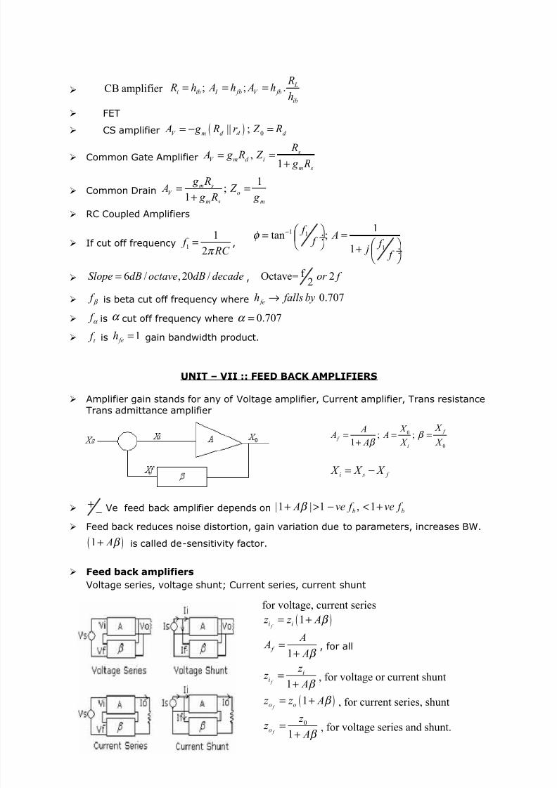
UNIT – VII :: FEED BAC AM,LIFIERS
)m%lifier gain stands for any of 2oltage am%lifier, urrent am%lifier, *rans resistance
*rans admittance am%lifier
+
− 2e feed back am%lifier de%ends on *1 * 1 , 1( (
A ve " ve " β + > − < +
Feed back reduces noise distortion, gain variation due to %arameters, increases !".
( )1 Aβ + is called de<sensitivity factor.
F""0 &; (!i.i"%*
2oltage series, voltage shunt; urrent series, current shunt
- 11 -
0
0
; ;1
"
"
i
& & A A A
A & & β
β = = =
+
i s " & & & = −
%o -ol+"e, cen+ seies
( )1 " i i
$ $ Aβ = +
1 "
A A
Aβ =
+, for all
1 "
ii
$ $
Aβ =
+
, %o -ol+"e o cen+ sn+
( )1 " o o
$ $ Aβ = + , %o cen+ seies, sn+
0
1 " o
$ $
Aβ =
+, %o -ol+"e seies "n sn+.

8/13/2019 Edc Brief Notes
http://slidepdf.com/reader/full/edc-brief-notes 12/13
UNIT – VIII :: OSCILLATORS
!arkausen riterion for oscillation loo% gain =H, θ =, A?.
')/*0E3 +-I00)*+/
/3-*)0 +-I00)*+/-
*uned ckt re%laced with rystal
8hase shift oscillator
"ein !ridge +scillator
- 12 -
1
2T
" L C π
= , 1 2T L L L 0 = + ± , ;
2
1
L
Lβ = ,
+008I*- +-I00)*+/,
1 2, L L re%laced by 1 2
,C C ,
re%laced by 0; 1
2T
" LC π
=
1 s
LC ω = ,
1 p
T LC
ω =
! !
1
2 6 "
'C π = , 29 A = ,
inimum / sections A
1 2 1 2
1
2 "
' ' C C π = ,
i% R1R2R, 12 ,1
2 "
'C π = ;
13 A
β = =
8 !
1
42 6
C
" '
'C '
π
= + ÷
, 29 A = ,
inimum / sections A

8/13/2019 Edc Brief Notes
http://slidepdf.com/reader/full/edc-brief-notes 13/13
- 13 -
Related Documents