4 de julio de 2013 Amplificador de señal AC con entrada filtrada Electrónica General Ródríguez - Rósales Pagina 1 1. TEMA: Diseño y construcción de un Amplificador de señal AC con señal de entrada filtrada. 2. OBJETIVOS: 2.1. Objetivo General: Aplicar los conocimientos adquiridos en el tercer parcial en la materia de electrónica general sobre Transistores BJT en el diseño y construcción de un Amplificador de señal AC con señal filtrada 2.2. Objetivos Específicos: Obtener cuatro salidas filtradas a partir de una señal de audio con los siguientes filtros: o Pasa-altas. o Pasa-Bajas. o Pasa-Banda. o Rechaza-Banda. Amplificar la señal obtenida luego de la fase de filtrado. Utilizar la señal amplificada para accionar un actuador. 3. MARCO TEÓRICO: FILTROS ACTIVOS Definición: Un filtro eléctrico es un cuadripolo capaz de atenuar determinadas frecuencias del espectro de la señal de entrada y permitir el paso de las demás. Se denomina espectro de una señal a su descomposición en una escala de amplitudes respecto de la frecuencia, y se hace por medio de las series de Fourier o con el analizador de espectro. Obsérvese que mientras el osciloscopio es un instrumento que analiza la señal en relación con el tiempo, el analizador lo hace por medio de las series de Fourier o con el analizador de espectro. Obsérvese que mientras el osciloscopio es un instrumento que analiza la señal en relación con el tiempo, el analizador lo hace con relación a la frecuencia. VENTAJAS E INCONVENIENTES DE LOS FILTROS ACTIVOS En comparación con los pasivos, los filtros activos poseen una serie de ventajas: - Permiten eliminar las inductancias que, en bajas frecuencias, son voluminosas, pesadas y caras. - Facilitan el diseño de filtros complejos mediante la asociación de etapas simples.

Welcome message from author
This document is posted to help you gain knowledge. Please leave a comment to let me know what you think about it! Share it to your friends and learn new things together.
Transcript

4 de julio de 2013 Amplificador de señal AC con entrada filtrada
Electró nica General Ródrí guez - Rósales Pa gina 1
1. TEMA:
Diseño y construcción de un Amplificador de señal AC con señal de entrada filtrada.
2. OBJETIVOS:
2.1. Objetivo General:
Aplicar los conocimientos adquiridos en el tercer parcial en la materia de
electrónica general sobre Transistores BJT en el diseño y construcción de un
Amplificador de señal AC con señal filtrada
2.2. Objetivos Específicos:
Obtener cuatro salidas filtradas a partir de una señal de audio con los
siguientes filtros:
o Pasa-altas.
o Pasa-Bajas.
o Pasa-Banda.
o Rechaza-Banda.
Amplificar la señal obtenida luego de la fase de filtrado.
Utilizar la señal amplificada para accionar un actuador.
3. MARCO TEÓRICO:
FILTROS ACTIVOS Definición: Un filtro eléctrico es un cuadripolo capaz de atenuar determinadas frecuencias del espectro de la señal de entrada y permitir el paso de las demás. Se denomina espectro de una señal a su descomposición en una escala de amplitudes respecto de la frecuencia, y se hace por medio de las series de Fourier o con el analizador de espectro. Obsérvese que mientras el osciloscopio es un instrumento que analiza la señal en relación con el tiempo, el analizador lo hace por medio de las series de Fourier o con el analizador de espectro. Obsérvese que mientras el osciloscopio es un instrumento que analiza la señal en relación con el tiempo, el analizador lo hace con relación a la frecuencia. VENTAJAS E INCONVENIENTES DE LOS FILTROS ACTIVOS En comparación con los pasivos, los filtros activos poseen una serie de ventajas: - Permiten eliminar las inductancias que, en bajas frecuencias, son voluminosas,
pesadas y caras. - Facilitan el diseño de filtros complejos mediante la asociación de etapas simples.

4 de julio de 2013 Amplificador de señal AC con entrada filtrada
Electró nica General Ródrí guez - Rósales Pa gina 2
- Proporcionan una gran amplificación de la señal de entrada (ganancia), lo que es importante al trabajar con señales de niveles muy bajos.
- Permiten mucha flexibilidad en los proyectos. Por otro lado, tienen una serie de inconvenientes: - Exigen una fuente de alimentación. - Su respuesta de frecuencia está limitada por la capacidad de los AO utilizados. - Es imposible su aplicación en sistemas de media y alta potencia (por ejemplo, en
los filtros que emplean los conversores e inversores construidos con tiristores que se utilizan en la industria).
A pesar de estas limitaciones, los filtros activos prestan cada vez un mayor servicio en el campo de la electrónica, especialmente en las áreas de instrumentación y telecomunicaciones. Dentro de la primera es interesante destacar la electromedicina o bioelectrónica, cuyos equipos hacen gran uso de ellos, principalmente cuando operan en bajas frecuencias. CLASIFICACION: Los filtros pueden clasificarse atendiendo a tres aspectos:
- a la función que llevan a cabo, - a la tecnología empleada, - a la función matemática utilizada para conseguir la curva de respuesta.
Al primer grupo pertenecen los cuatro tipos siguientes:
- FUNCION QUE LLEVAN A CABO
a. Filtro pasa bajo (PB) Sólo permite el paso de las frecuencias inferiores a una determinada fc (denominada de corte). Las frecuencias superiores resultan atenuadas. b. Filtro pasa alto (PA) Deja pasar las frecuencias que se hallan por encima de una determinada fc (de corte) atenuando las inferiores. c. Filtro pasa banda (PBANDA) Permite el paso de las frecuencias situadas dentro de una banda delimitada por una frecuencia de corte inferior (fc1) y otra superior (fc2). Las frecuencias que estén fuera de esta banda son atenuadas. d. Filtro de rechazo de banda (RB) Permite el paso de las frecuencias inferiores o superiores a dos frecuencias determinadas, que se denominan de corte inferior (fc1) y superior (fc2),

4 de julio de 2013 Amplificador de señal AC con entrada filtrada
Electró nica General Ródrí guez - Rósales Pa gina 3
respectivamente. Son atenuadas las frecuencias comprendidas en la banda que delimitan fc1 y fc2.
Dentro del segundo grupo los filtros se clasifican atendiendo a la tecnología empleada:
- TECNOLOGIA EMPLEADA a: Filtros pasivos.- Están construidos exclusivamente con elementos pasivos como resistencias, condensadores y bobinas. Estos filtros son inviables en bajas frecuencias al exigir inductancias muy grandes. b. Filtros activos.- Constan de elementos pasivos asociados a otros activos (válvulas, transistores o amplificadores operacionales). La primera generación de estos filtros utilizaba las válvulas, por lo que tenían un consumo de potencia muy alto, ruidos, baja ganancia, etc. La segunda empleaba transistores como elementos activos y, aunque tenía más ventajas que la anterior, no tenía unas características enteramente satisfactorias. La tercera generación, objeto de nuestro estudio, utiliza los amplificadores operacionales. La alta resistencia de entrada y la baja resistencia de salida de los AOP’s, además de otras características, permiten la realización de filtros con cualidades óptimas. c. Filtros digitales.- Estos filtros llevan componentes digitales. La señal analógica es convertida en digital mediante un sistema de conversión A/D. La señal binaria resultante se trata en el filtro digital y a continuación se reconvierte en analógica en un conversor D/A. Estos filtros son útiles para procesar simultáneamente muchos canales de transmisión.

4 de julio de 2013 Amplificador de señal AC con entrada filtrada
Electró nica General Ródrí guez - Rósales Pa gina 4
- FUNCIONES MATEMATICAS Para finalizar, el tercer grupo de la clasificación hacía referencia a la función matemática (o aproximación) utilizada para proyectar el filtro. Un estudio detallado de este tema escapa a nuestras intenciones, ya que exige un tratamiento matemático complejo y de interés puramente teórico. Los tipos más comunes de aproximaciones son los siguientes:
- Butterworth. - Chebyshev. - Cauer.
Cada uno tiene una función matemática específica que permite aproximar su curva de respuesta a la ideal de cada tipo de filtro. En las secciones siguientes se estudiarán los dos primeros, por ser los más sencillos y los más utilizados en la práctica. La función de Cauer, denominada también elíptica, es la de mayor exactitud, pero su complejidad impide abordarla con detalle. FILTROS BUTTERWORTH PASA BAJOS En diversas aplicaciones de los filtros pasa bajos se necesita que la ganancia de lazo cerrado se aproxime lo más posible a 1 dentro de la banda de paso. Para este tipo de aplicación, lo mejor es el filtro Butterworth. A este tipo de filtro también se le conoce como filtro máximamente plano o plano-plano. Todos los filtros utilizados en esta sección serán del tipo Butterworth. A continuación se muestra en la figura la respuesta a la frecuencia ideal (línea continua) y la respuesta a la frecuencia real (línea punteada), de tres tipos de filtros Butterworth. Conforme las atenuaciones se van volviendo más pronunciadas, podemos observar que se acerca más al filtro ideal. Para obtener un filtro de -40 db/dec se podrían acoplar dos filtros activos similares, sin embargo este no es el diseño más económico, ya que para ello se necesitan dos amplificadores operacionales. A continuación veremos como construir un filtro Butterworth de -40 db/dec (2° Orden), con un Amplificador Operacional. Para obtener un filtro de -60 db/dec se podrían acoplar tres filtros activos similares, sin embargo este no es el diseño más económico, ya que para ello se necesitan tres amplificadores operacionales. Se podría construir con un filtro de -40 db/dec, conectado en cascada con un filtro de -20 db/dec.
4 de julio de 2013 Amplificador de señal AC con entrada filtrada
Electró nica General Ródrí guez - Rósales Pa gina 5
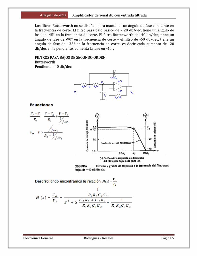
Los filtros Butterworth no se diseñan para mantener un ángulo de fase constante en la frecuencia de corte. El filtro pasa bajo básico de – 20 db/dec, tiene un ángulo de fase de -45° en la frecuencia de corte. El filtro Butterworth de -40 db/dec, tiene un ángulo de fase de -90° en la frecuencia de corte y el filtro de -60 db/dec, tiene un ángulo de fase de 135° en la frecuencia de corte, es decir cada aumento de -20 db/dec en la pendiente, aumenta la fase en -45°. FILTROS PASA BAJOS DE SEGUNDO ORDEN Butterworth Pendiente: -40 db/dec

4 de julio de 2013 Amplificador de señal AC con entrada filtrada
Electró nica General Ródrí guez - Rósales Pa gina 6

4 de julio de 2013 Amplificador de señal AC con entrada filtrada
Electró nica General Ródrí guez - Rósales Pa gina 7
FILTROS BUTTERWORTH PASA ALTOS Los filtros pasa altos son circuitos que atenúan todas las señales cuya frecuencia está por debajo de una frecuencia de corte específica, f, y pasa todas aquellas señales cuya frecuencia es superior a la frecuencia de corte. Es decir, el filtro pasa altos funciona en forma contraria al filtro pasa bajos. La figura muestra a continuación una gráfica de la magnitud de la ganancia de lazo cerrado en función de w para tres tipos de filtros Butterworth. El ángulo de fase de un circuito de +20 db/dec es 45° para la frecuencia w.
FILTROS BUTTERWORTH PASA ALTOS DE SEGUNDO ORDEN Pendiente: +40 db/dec

4 de julio de 2013 Amplificador de señal AC con entrada filtrada
Electró nica General Ródrí guez - Rósales Pa gina 8

4 de julio de 2013 Amplificador de señal AC con entrada filtrada
Electró nica General Ródrí guez - Rósales Pa gina 9
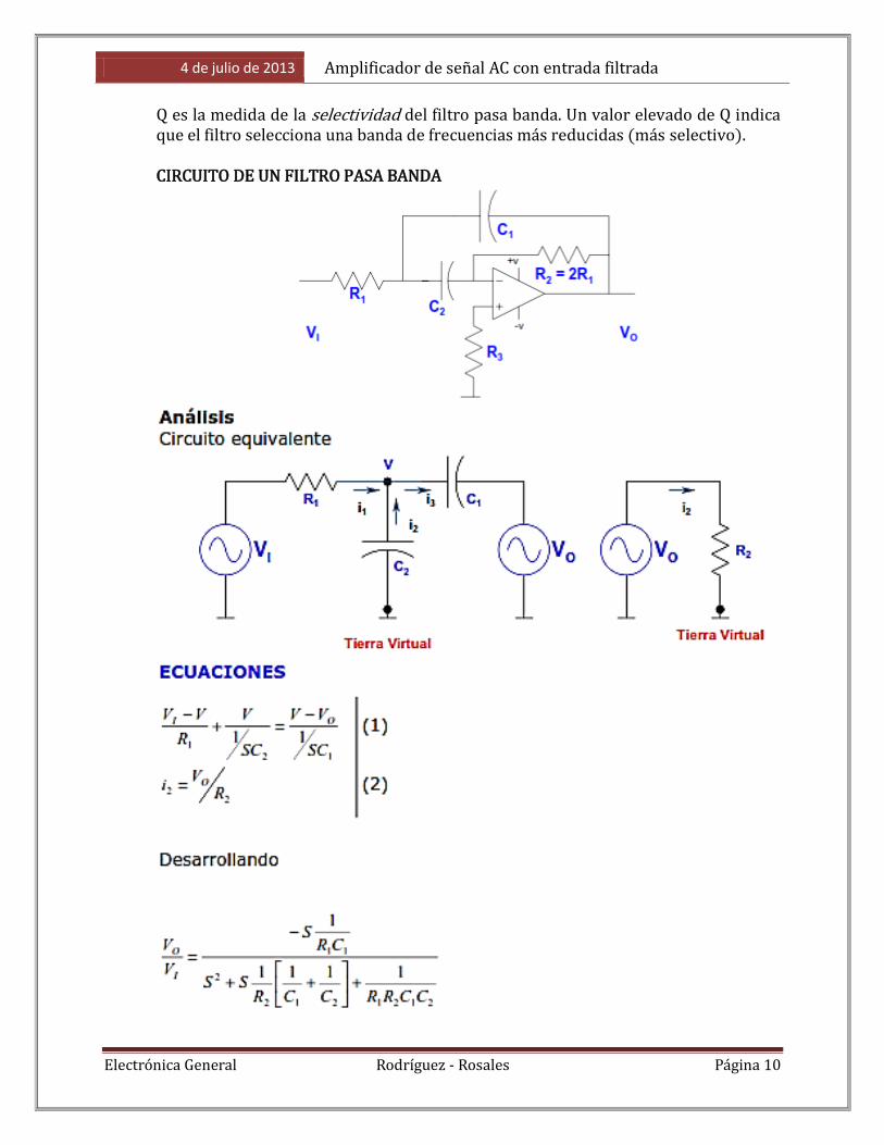
FILTROS PASA BANDA Los filtros pasa banda son selectores de frecuencia. Permiten a uno elegir o pasar sólo una determinada banda de frecuencias de entre todas las frecuencias que puede haber en un circuito. En la siguiente figura se puede apreciar la respuesta de frecuencia normalizada de este filtro. Este tipo de filtros tiene una ganancia máxima en la frecuencia de resonancia fr. Dado que se trata de un filtro “normalizado”, se trabajará con ganancia unitaria a fr y las frecuencias de corte estarán ubicadas 0,707 del valor máximo.
DEFINICIONES Ancho de Banda: Al rango de frecuencias comprendidas entre fi y fh se le conoce como ancho de banda, Bw o:
Bw = fh – fl El ancho de banda no se encuentra centrado justamente en la frecuencia de resonancia. (Por ello se utilizará el nombre de “frecuencia resonante” y no el de “frecuencia central”, para referirse a la fr). Si se conocen los valores de fl y de fh, la frecuencia resonante se puede calcular mediante la siguiente expresión:
√
Si se conoce la frecuencia resonante fr y el ancho de banda BW, mediante la siguiente ecuación se calculan las frecuencias de corte:
Factor de Calidad: El factor de calidad, Q, se define como la relación entre la frecuencia resonante y el ancho de banda, es decir:
4 de julio de 2013 Amplificador de señal AC con entrada filtrada
Electró nica General Ródrí guez - Rósales Pa gina 10
Q es la medida de la selectividad del filtro pasa banda. Un valor elevado de Q indica que el filtro selecciona una banda de frecuencias más reducidas (más selectivo). CIRCUITO DE UN FILTRO PASA BANDA

4 de julio de 2013 Amplificador de señal AC con entrada filtrada
Electró nica General Ródrí guez - Rósales Pa gina 11
FILTROS SUPRESORES DE BANDA o FILTROS NOTCH El nombre de filtro de rechazo de banda o supresor de banda o filtro de muesca, se debe a la forma característica de su curva de respuesta a la frecuencia, la cual se muestra a continuación.
Las frecuencias indeseables se atenúan en la banda de rechazo, Bw. Las frecuencias deseadas sí se transmiten y son las que se encuentran dentro de las bandas que están a ambos lados de la muesca. Por lo general la ganancia de la banda de paso de los filtros supresores es de 1 o 0 db. Las ecuaciones correspondientes a Q, Bw, fl, fh y fr son idénticas a la del filtro pasa banda correspondiente. PARA QUE SIRVE UN FILTRO SUPRESOR En las aplicaciones en las que se necesita amplificar señales de bajo nivel, existe la posibilidad de que haya una o varias señales de ruido indeseables. Por ejemplo, las frecuencias de 50,60 o 400 Hz de las líneas de suministro eléctrico; el rizado de 100 Hz que producen los rectificadores de onda completa, o incluso, frecuencias más

4 de julio de 2013 Amplificador de señal AC con entrada filtrada
Electró nica General Ródrí guez - Rósales Pa gina 12
altas que generan las fuentes de alimentación reguladas conmutadas o los osciladores de reloj. Si ambas señales y un componente de ruido de la misma frecuencia se pasan por el filtro supresor, únicamente saldrá del filtro las señales deseadas. La frecuencia de ruido se suprime con la muesca.
FILTRO ACTIVO NOTCH

4 de julio de 2013 Amplificador de señal AC con entrada filtrada
Electró nica General Ródrí guez - Rósales Pa gina 13
FUENTE ELÉCTRICA:
Se considera una fuente eléctrica al elemento activo de un circuito que es capaz de
generar una diferencia de potencial entre sus bornes o proporcionar una corriente
eléctrica para que otros circuitos funcionen.
Representación esquemática de fuentes de tensión y de corriente.
Para la realización de este proyecto, utilizaremos como fuente de tensión alterna el
tomacorriente estándar ecuatoriano, el mismo que proporciona un voltaje RMS de 110
V aproximadamente y trabaja a una frecuencia de 60 Hz.

4 de julio de 2013 Amplificador de señal AC con entrada filtrada
Electró nica General Ródrí guez - Rósales Pa gina 14
CAPACITOR O CONDENSADOR ELÉCTRICO:
Un condensador es un dispositivo pasivo, utilizado en electricidad y electrónica, capaz
de almacenar energía sustentando un campo eléctrico. Está formado por un par de
superficies conductoras, generalmente en forma de láminas o placas, en situación
de influencia total separadas por un material dieléctrico o por el vacío. Las placas,
sometidas a una diferencia de potencial, adquieren una determinada carga eléctrica,
positiva en una de ellas y negativa en la otra, siendo nula la variación de carga total.
Condensadores comerciales.
Aunque desde el punto de vista físico un condensador no almacena carga ni corriente
eléctrica, sino simplemente energía mecánica latente; al ser introducido en
un circuito se comporta en la práctica como un elemento "capaz" de almacenar
la energía eléctrica que recibe durante el periodo de carga, la misma energía que cede
después durante el periodo de descarga.
RESISTENCIA ELÉCTRICA:
La resistencia eléctrica de un objeto es una medida de su oposición al paso de corriente
y es directamente proporcional a la longitud e inversamente proporcional a su sección
transversal:
Donde ρ es el coeficiente de proporcionalidad o la resistividad del material.
Descubierta por Georg Ohm en 1827.
La unidad de la resistencia en el SI es el ohmio (Ω).

4 de julio de 2013 Amplificador de señal AC con entrada filtrada
Electró nica General Ródrí guez - Rósales Pa gina 15
La resistencia de cualquier objeto depende de su geometría y de su coeficiente de
resistividad a determinada temperatura. La misma aumenta conforme es mayor su
longitud y disminuye conforme aumenta su grosor o sección transversal.
De acuerdo con la ley de Ohm la resistencia de un material puede definirse como la
razón entre la caída de tensión y la corriente en dicha resistencia, así:
Donde R es la resistencia en ohmios, V es la diferencia de potencial en voltios e I es la
intensidad de corriente en amperios.
En el caso de que la señal aplicada a una resistencia sea sinusoidal, corriente alterna
(CA), a bajas frecuencias se observa que una resistencia real se comportará de forma
muy similar a como lo haría en CC, siendo despreciables las diferencias. En altas
frecuencias el comportamiento es diferente, aumentando en la medida en la que
aumenta la frecuencia aplicada, lo que se explica fundamentalmente por los efectos
inductivos que producen los materiales que conforman la resistencia real.
Sea una resistencia R y un diferencial de potencial u(t):
De acuerdo con la ley de Ohm circulará una corriente alterna de valor:
Donde . Se obtiene así, para la corriente, una función sinusoidal que está en
fase con la tensión aplicada.

4 de julio de 2013 Amplificador de señal AC con entrada filtrada
Electró nica General Ródrí guez - Rósales Pa gina 16
Si se representa el valor eficaz de la corriente obtenida en forma polar:
Se deduce que en los circuitos de CA la resistencia puede considerarse como una
magnitud compleja con parte real y sin parte imaginaria o, lo que es lo mismo con
argumento nulo, cuya representación binómica y polar serán:
POTENCIÓMETRO:
Un potenciómetro es un resistor cuyo valor de resistencia es variable. De esta manera,
indirectamente, se puede controlar la intensidad de corriente que fluye por un circuito
si se conecta en paralelo, o la diferencia de potencial al conectarlo en serie.
Normalmente, los potenciómetros se utilizan en circuitos de poca corriente. Para
circuitos de corrientes mayores, se utilizan los reostatos, que pueden disipar más
potencia.
Potenciómetros comerciales.
TRANSISTOR:
El transistor de unión bipolar (del inglés Bipolar Junction Transistor, o sus siglas BJT) es
un dispositivo electrónico de estado sólido consistente en dos uniones PN muy cercanas

4 de julio de 2013 Amplificador de señal AC con entrada filtrada
Electró nica General Ródrí guez - Rósales Pa gina 17
entre sí, que permite controlar el paso de la corriente a través de sus terminales. La
denominación de bipolar se debe a que la conducción tiene lugar gracias al desplazamiento
de portadores de dos polaridades (huecos positivos y electrones negativos), y son de gran
utilidad en gran número de aplicaciones; pero tienen ciertos inconvenientes, entre ellos
su impedancia de entrada bastante baja.
Los transistores bipolares son los transistores más conocidos y se usan generalmente
en electrónica analógica aunque también en algunas aplicaciones deelectrónica digital,
como la tecnología TTL o BICMOS.
Un transistor de unión bipolar está formado por dos Uniones PN en un solo cristal
semiconductor, separados por una región muy estrecha. De esta manera quedan formadas
tres regiones:
Emisor, que se diferencia de las otras dos por estar fuertemente dopada,
comportándose como un metal. Su nombre se debe a que esta terminal funciona
como emisor de portadores de carga.
Base, la intermedia, muy estrecha, que separa el emisor del colector.
Colector, de extensión mucho mayor.
La técnica de fabricación más común es la deposición epitaxial. En su funcionamiento
normal, la unión base-emisor está polarizada en directa, mientras que la base-colector en
inversa. Los portadores de carga emitidos por el emisor atraviesan la base, porque es muy
angosta, hay poca recombinación de portadores, y la mayoría pasa al colector. El transistor
posee tres estados de operación: estado de corte, estado de saturación y estado de
actividad.
Estructura

4 de julio de 2013 Amplificador de señal AC con entrada filtrada
Electró nica General Ródrí guez - Rósales Pa gina 18
Un transistor de unión bipolar consiste en tres regiones semiconductoras dopadas: la
región del emisor, la región de la base y la región del colector. Estas regiones son,
respectivamente, tipo P, tipo N y tipo P en un PNP, y tipo N, tipo P, y tipo N en un transistor
NPN. Cada región del semiconductor está conectada a un terminal, denominado emisor (E),
base (B) o colector (C), según corresponda.
Corte transversal simplificado de un transistor de unión bipolar NPN. Donde se puede
apreciar como la unión base-colector es mucho más amplia que la base-emisor.
La base está físicamente localizada entre el emisor y el colector y está compuesta de
material semiconductor ligeramente dopado y de alta resistividad. El colector rodea la
región del emisor, haciendo casi imposible para los electrones inyectados en la región de la
base escapar de ser colectados, lo que hace que el valor resultante de α se acerque mucho
hacia la unidad, y por eso, otorgarle al transistor un gran β.
El transistor de unión bipolar, a diferencia de otros transistores, no es usualmente un
dispositivo simétrico. Esto significa que intercambiando el colector y el emisor hacen que el
transistor deje de funcionar en modo activo y comience a funcionar en modo inverso.
Debido a que la estructura interna del transistor está usualmente optimizada para
funcionar en modo activo, intercambiar el colector con el emisor hacen que los valores de α
y β en modo inverso sean mucho más pequeños que los que se podrían obtener en modo
activo; muchas veces el valor de α en modo inverso es menor a 0.5. La falta de simetría es
principalmente debido a las tasas de dopaje entre el emisor y el colector. El emisor está
altamente dopado, mientras que el colector está ligeramente dopado, permitiendo que
pueda ser aplicada una gran tensión de reversa en la unión colector-base antes de que esta
colapse. La unión colector-base está polarizada en inversa durante la operación normal. La
razón por la cual el emisor está altamente dopado es para aumentar la eficiencia de
inyección de portadores del emisor: la tasa de portadores inyectados por el emisor en
relación con aquellos inyectados por la base. Para una gran ganancia de corriente, la
mayoría de los portadores inyectados en la unión base-emisor deben provenir del emisor.
El bajo desempeño de los transistores bipolares laterales muchas veces utilizados en
procesos CMOS es debido a que son diseñados simétricamente, lo que significa que no hay
diferencia alguna entre la operación en modo activo y modo inverso.
Pequeños cambios en la tensión aplicada entre los terminales base-emisor genera que la
corriente que circula entre el emisor y el colector cambie significativamente. Este efecto
puede ser utilizado para amplificar la tensión o corriente de entrada. Los BJT pueden ser

4 de julio de 2013 Amplificador de señal AC con entrada filtrada
Electró nica General Ródrí guez - Rósales Pa gina 19
pensados como fuentes de corriente controladas por tensión, pero son caracterizados más
simplemente como fuentes de corriente controladas por corriente, o por amplificadores de
corriente, debido a la baja impedancia de la base.
Los primeros transistores fueron fabricados de germanio, pero la mayoría de los BJT
modernos están compuestos de silicio. Actualmente, una pequeña parte de éstos (los
transistores bipolares de heterojuntura) están hechos de arseniuro de galio, especialmente
utilizados en aplicaciones de alta velocidad.
Funcionamiento
Característica idealizada de un transistor bipolar.
En una configuración normal, la unión emisor-base se polariza en directa y la unión base-
colector en inversa. Debido a la agitación térmica los portadores de carga del emisor
pueden atravesar la barrera de potencial emisor-base y llegar a la base. A su vez,
prácticamente todos los portadores que llegaron son impulsados por el campo eléctrico
que existe entre la base y el colector.
Un transistor NPN puede ser considerado como dos diodos con la región del ánodo
compartida. En una operación típica, la unión base-emisor está polarizada en directa y la
unión base-colector está polarizada en inversa. En un transistor NPN, por ejemplo, cuando
una tensión positiva es aplicada en la unión base-emisor, el equilibrio entre los portadores
generados térmicamente y el campo eléctrico repelente de la región agotada se
desbalancea, permitiendo a los electrones excitados térmicamente inyectarse en la región
de la base. Estos electrones "vagan" a través de la base, desde la región de alta
concentración cercana al emisor hasta la región de baja concentración cercana al colector.
Estos electrones en la base son llamados portadores minoritarios debido a que la base
está dopada con material P, los cuales generan "huecos" como portadores mayoritarios en
la base.
La región de la base en un transistor debe ser constructivamente delgada, para que los
portadores puedan difundirse a través de esta en mucho menos tiempo que la vida útil del

4 de julio de 2013 Amplificador de señal AC con entrada filtrada
Electró nica General Ródrí guez - Rósales Pa gina 20
portador minoritario del semiconductor, para minimizar el porcentaje de portadores que
se recombinan antes de alcanzar la unión base-colector. El espesor de la base debe ser
menor al ancho de difusión de los electrones.
Control de tensión, carga y corriente
La corriente colector-emisor puede ser vista como controlada por la corriente base-emisor
(control de corriente), o por la tensión base-emisor (control de voltaje). Esto es debido a la
relación tensión-corriente de la unión base-emisor, la cual es la curva tensión-corriente
exponencial usual de una unión PN (es decir, un diodo).
En el diseño de circuitos analógicos, el control de corriente es utilizado debido a que es
aproximadamente lineal. Esto significa que la corriente de colector es aproximadamente β
veces la corriente de la base. Algunos circuitos pueden ser diseñados asumiendo que la
tensión base-emisor es aproximadamente constante, y que la corriente de colector es β
veces la corriente de la base. No obstante, para diseñar circuitos utilizando BJT con
precisión y confiabilidad, se requiere el uso de modelos matemáticos del transistor como
el modelo Ebers-Moll.
El Alfa y Beta del transistor
Una forma de medir la eficiencia del BJT es a través de la proporción de electrones capaces
de cruzar la base y alcanzar el colector. El alto dopaje de la región del emisor y el bajo
dopaje de la región de la base pueden causar que muchos más electrones sean inyectados
desde el emisor hacia la base que huecos desde la base hacia el emisor. La ganancia de
corriente emisor comúnestá representada por o por hfe. Esto es aproximadamente la
tasa de corriente continua de colector a la corriente continua de la base en la región activa
directa y es típicamente mayor a 100. Otro parámetro importante es la ganancia de
corriente base común, . La ganancia de corriente base común es aproximadamente la
ganancia de corriente desde emisor a colector en la región activa directa. Esta tasa
usualmente tiene un valor cercano a la unidad; que oscila entre 0.98 y 0.998. El Alfa y Beta
están más precisamente determinados por las siguientes relaciones (para un transistor
NPN):

4 de julio de 2013 Amplificador de señal AC con entrada filtrada
Electró nica General Ródrí guez - Rósales Pa gina 21
Tipos de Transistor de Unión Bipolar
NPN
El símbolo de un transistor NPN.
NPN es uno de los dos tipos de transistores bipolares, en los cuales las letras "N"
y "P" se refieren a los portadores de carga mayoritarios dentro de las diferentes
regiones del transistor. La mayoría de los transistores bipolares usados hoy en
día son NPN, debido a que la movilidad del electrón es mayor que la movilidad
de los "huecos" en los semiconductores, permitiendo mayores corrientes y
velocidades de operación.
Los transistores NPN consisten en una capa de material
semiconductor dopado P (la "base") entre dos capas de material dopado N. Una
pequeña corriente ingresando a la base en configuración emisor-común es
amplificada en la salida del colector.
La flecha en el símbolo del transistor NPN está en la terminal del emisor y
apunta en la dirección en la que la corriente convencional circula cuando el
dispositivo está en funcionamiento activo.
PNP
El otro tipo de transistor de unión bipolar es el PNP con las letras "P" y "N"
refiriéndose a las cargas mayoritarias dentro de las diferentes regiones del
transistor. Pocos transistores usados hoy en día son PNP, debido a que el NPN
brinda mucho mejor desempeño en la mayoría de las circunstancias.

4 de julio de 2013 Amplificador de señal AC con entrada filtrada
Electró nica General Ródrí guez - Rósales Pa gina 22
El símbolo de un transistor PNP.
Los transistores PNP consisten en una capa de material
semiconductor dopado N entre dos capas de material dopado P. Los transistores
PNP son comúnmente operados con el colector a masa y el emisor conectado al
terminal positivo de la fuente de alimentación a través de una carga eléctrica
externa. Una pequeña corriente circulando desde la base permite que una
corriente mucho mayor circule desde el emisor hacia el colector.
La flecha en el transistor PNP está en el terminal del emisor y apunta en la
dirección en la que la corriente convencional circula cuando el dispositivo está
en funcionamiento activo.
Regiones operativas del transistor
Los transistores de unión bipolar tienen diferentes regiones operativas, definidas
principalmente por la forma en que son polarizados:
Región activa:
Corriente del emisor (β 1)·Ib ; corriente del colector β·Ib
Cuando un transistor no está ni en su región de saturación ni en la región de corte
entonces está en una región intermedia, la región activa. En esta región la corriente
de colector (Ic) depende principalmente de la corriente de base (Ib), de β (ganancia
de corriente, es un dato del fabricante) y de las resistencias que se encuentren
conectadas en el colector y emisor. Esta región es la más importante si lo que se
desea es utilizar el transistor como un amplificador de señal.
Región inversa:
Al invertir las condiciones de polaridad del funcionamiento en modo activo, el

4 de julio de 2013 Amplificador de señal AC con entrada filtrada
Electró nica General Ródrí guez - Rósales Pa gina 23
transistor bipolar entra en funcionamiento en modo inverso. En este modo, las
regiones del colector y emisor intercambian roles. Debido a que la mayoría de los
BJT son diseñados para maximizar la ganancia de corriente en modo activo, el
parámetro beta en modo inverso es drásticamente menor al presente en modo
activo.
Región de corte: Un transistor está en corte cuando:
Corriente de colector = corriente de emisor = 0, (Ic = Ie = 0)
En este caso el voltaje entre el colector y el emisor del transistor es el voltaje de
alimentación del circuito. (como no hay corriente circulando, no hay caída de voltaje,
ver Ley de Ohm). Este caso normalmente se presenta cuando la corriente de base
0 (Ib 0)
De forma simplificada, se puede decir que el la unión CE se comporta como un
circuito abierto, ya que la corriente que lo atraviesa es cero.
Región de saturación: Un transistor está saturado cuando:
Corriente de colector ≈ corriente de emisor corriente maxima, (Ic ≈ Ie = Imax)
En este caso la magnitud de la corriente depende del voltaje de alimentación del
circuito y de las resistencias conectadas en el colector o el emisor o en ambos,
ver Ley de Ohm. Se presenta cuando la diferencia de potencial entre el colector y el
emisor desciende por debajo del valor umbral VCE,sat. Cuando el transistor esta en
saturación, la relación lineal de amplificación Ic β·Ib (y por ende, la relación
Ie (β 1)·Ib ) no se cumple.
De forma simplificada, se puede decir que la unión CE se comporta como un cable,
ya que la diferencia de potencial entre C y E es muy próxima a cero.
Como se puede ver, la región activa es útil para la electrónica analógica (especialmente útil
para amplificación de señal) y las regiones de corte y saturación, para la electrónica digital,
representando el estado lógico alto y bajo, respectivamente.
Historia
Réplica del primer transistor.

4 de julio de 2013 Amplificador de señal AC con entrada filtrada
Electró nica General Ródrí guez - Rósales Pa gina 24
El transistor bipolar fue inventado en Diciembre de 1947 en la Bell Telephone
Company por John Bardeen y Walter Brattain bajo la dirección de William Shockley. La
versión de unión, inventada por Shockley en 1948, fue durante tres décadas el dispositivo
favorito en diseño de circuitos discretos e integrados. Hoy en día, el uso de BJT ha
declinado en favor de la tecnología CMOS para el diseño de circuitos digitales integrados.
Teoría y Modelos Matemáticos
Análisis en continua
El modelo Ebers-Moll
Las corrientes continuas en el emisor y el colector en operación normal son determinadas
por:
t
Modelo Ebers-Moll para transistores NPN
Modelo Ebers-Moll para transistores PNP
La corriente interna de base es principalmente por difusión y
Dónde:
es la corriente de emisor.
es la corriente de colector.
es la ganancia de corriente directa en configuración base común. (de 0.98 a 0.998)

4 de julio de 2013 Amplificador de señal AC con entrada filtrada
Electró nica General Ródrí guez - Rósales Pa gina 25
es la corriente de saturación inversa del diodo base-emisor (en el orden de 10−15 a
10−12 amperios)
es el voltaje térmico (aproximadamente 26 mV a temperatura ambiente ≈
300 K).
es la tensión base emisor.
W es el ancho de la base.
La corriente de colector es ligeramente menor a la corriente de emisor, debido a que el
valor de αT es muy cercano a 1,0. En el transistor de unión bipolar una pequeña variación
de la corriente base-emisor genera un gran cambio en la corriente colector-emisor. La
relación entre la corriente colector-emisor con la base-emisor es llamada ganancia, β o hFE.
Un valor de β de 100 es típico para pequeños transistores bipolares. En una configuración
típica, una señal de corriente muy débil circula a través de la unión base-emisor para
controlar la corriente entre emisor-colector. β está relacionada con α a través de las
siguientes relaciones:
Eficiencia del emisor:
Otras ecuaciones son usadas para describir las tres corrientes en cualquier región del
transistor están expresadas más abajo. Estas ecuaciones están basadas en el modelo de
transporte de un transistor de unión bipolar.
Dónde:
es la corriente de colector.
es la corriente de base.
es la corriente de emisor.

4 de julio de 2013 Amplificador de señal AC con entrada filtrada
Electró nica General Ródrí guez - Rósales Pa gina 26
es la ganancia activa en emisor común (de 20 a 500)
es la ganancia inversa en emisor común (de 0 a 20)
es la corriente de saturación inversa (en el orden de 10−15 a 10−12 amperios)
es el voltaje térmico (aproximadamente 26 mV a temperatura ambiente ≈
300 K).
es la tensión base-emisor.
es la tensión base-colector.
Modelo en pequeña señal
Parámetros h
Otro modelo comúnmente usado para analizar los circuitos BJT es el modelo de parámetro
h. Este modelo es un circuito equivalente a un transistor de unión bipolar y permite un fácil
análisis del comportamiento del circuito, y puede ser usado para desarrollar modelos más
exactos. Como se muestra, el término "x" en el modelo representa el terminal del BJT
dependiendo de la topología usada. Para el modo emisor-común los varios símbolos de la
imagen toman los valores específicos de:
x 'e' debido a que es una configuración emisor común.
Terminal 1 Base
Terminal 2 Colector
Terminal 3 Emisor
iin Corriente de Base (ib)
io Corriente de Colector (ic)
Vin Tensión Base-Emisor (VBE)
Vo Tensión Colector-Emisor (VCE)
Y los parámetros h están dados por:
hix hie - La impedancia de entrada del transistor (correspondiente a la
resistencia del emisor re).

4 de julio de 2013 Amplificador de señal AC con entrada filtrada
Electró nica General Ródrí guez - Rósales Pa gina 27
hrx hre - Representa la dependencia de la curva IB–VBE del transistor en el valor
de VCE. Es usualmente un valor muy pequeño y es generalmente despreciado (se
considera cero).
hfx hfe - La ganancia de corriente del transistor. Este parámetro es
generalmente referido como hFE o como la ganancia de corriente continua (βDC)
in en las hojas de datos.
hox hoe - La impedancia de salida del transistor. Este término es usualmente
especificado como una admitancia, debiendo ser invertido para convertirlo a
impedancia.
Como se ve, los parámetros h tienen subíndices en minúscula y por ende representan que
las condiciones de análisis del circuito son con corrientes alternas. Para condiciones
de corriente continua estos subíndices son expresados en mayúsculas. Para la topología
emisor común, un aproximado del modelo de parámetro h es comúnmente utilizado ya que
simplifica el análisis del circuito. Por esto los parámetros hoe y hre son ignorados (son
tomados como infinito y cero, respectivamente). También debe notarse que el modelo de
parámetro h es sólo aplicable al análisis de señales débiles de bajas frecuencias. Para
análisis de señales de altas frecuencias este modelo no es utilizado debido a que ignora las
capacitancias entre electrodos que entran en juego a altas frecuencias.
4. MATERIALES Y EQUIPOS: o Protoboard o Resistencias varias o Amplificadores operacionales LM358 o Capacitores diversos valores o Transistores BJT 3904 o Diodos LEDs alto brillo o Motor 1,5 V o Cable auxiliar o Entrada audio o Dispositivo de música
4 de julio de 2013 Amplificador de señal AC con entrada filtrada
Electró nica General Ródrí guez - Rósales Pa gina 28
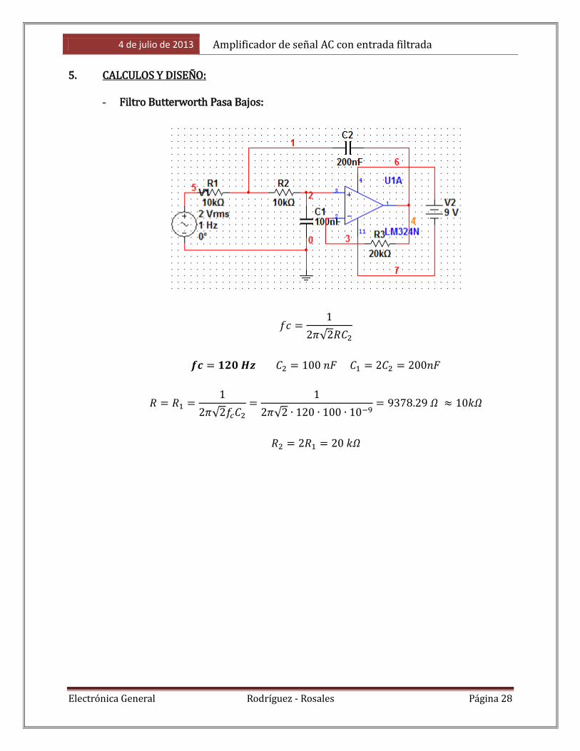
5. CALCULOS Y DISEÑO: - Filtro Butterworth Pasa Bajos:
𝑐 1
2𝜋√2𝑅𝐶2
𝒇𝒄 𝟏𝟐𝟎 𝑯𝒛 𝐶2 100 𝑛𝐹 𝐶1 2𝐶2 200𝑛𝐹
𝑅 𝑅1 1
2𝜋√2 𝑐𝐶2
1
2𝜋√2 ∙ 120 ∙ 100 ∙ 10−9 9378.29 𝛺 ≈ 10𝑘𝛺
𝑅2 2𝑅1 20 𝑘𝛺
4 de julio de 2013 Amplificador de señal AC con entrada filtrada
Electró nica General Ródrí guez - Rósales Pa gina 29
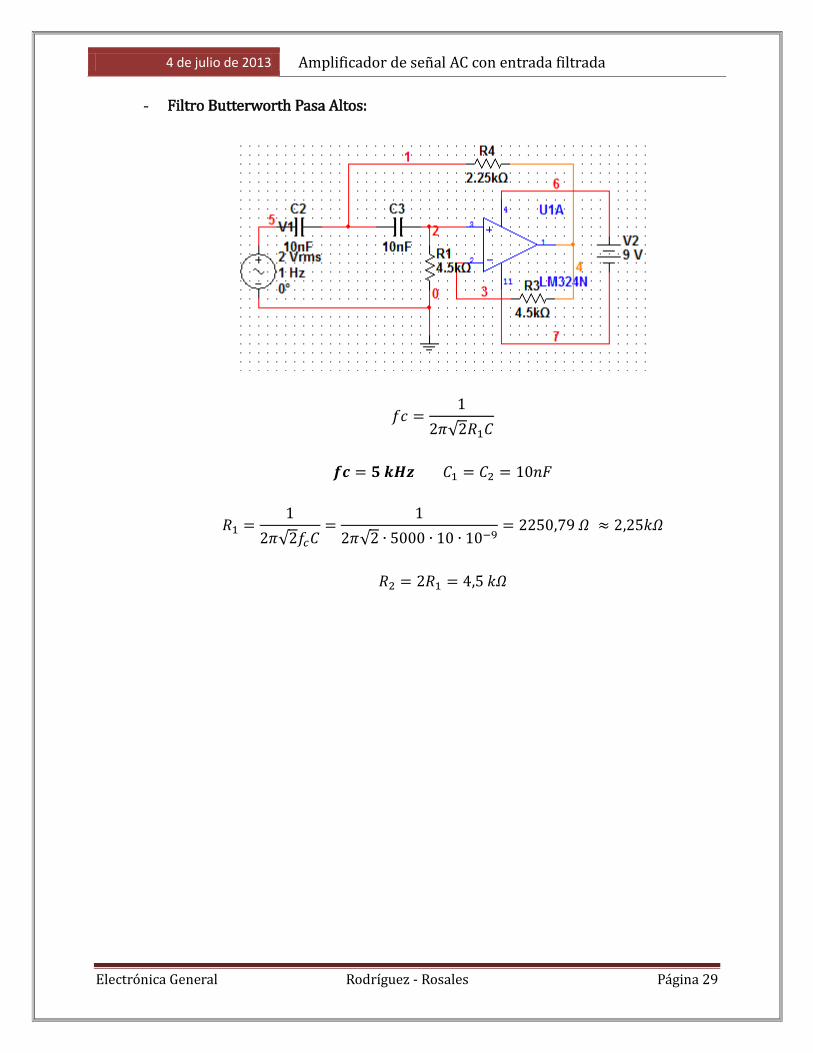
- Filtro Butterworth Pasa Altos:
𝑐 1
2𝜋√2𝑅1𝐶
𝒇𝒄 𝟓 𝒌𝑯𝒛 𝐶1 𝐶2 10𝑛𝐹
𝑅1 1
2𝜋√2 𝑐𝐶
1
2𝜋√2 ∙ 5000 ∙ 10 ∙ 10−9 2250,79 𝛺 ≈ 2,25𝑘𝛺
𝑅2 2𝑅1 4,5 𝑘𝛺

4 de julio de 2013 Amplificador de señal AC con entrada filtrada
Electró nica General Ródrí guez - Rósales Pa gina 30
- Filtro Butterworth Pasa Bandas:
1
2𝜋𝑅𝐶
𝒇𝒓 𝟏𝟓𝟎𝟎 𝑯𝒛 𝐶1 𝐶2 𝐶 10𝑛𝐹
𝑅 1
2𝜋 𝐶
1
2𝜋 ∙ 1500 ∙ 10 ∙ 10−9 10610 𝛺
𝐺𝑎𝑛𝑎𝑛𝑐𝑖𝑎 1 2 2 → 0.707
𝑅1 𝑅
2 7500 𝛺 𝑅2 2 𝑅 15 𝑘𝛺
1060.66 1 439.34 𝐻𝑧 2 2560.66 𝐻𝑧

4 de julio de 2013 Amplificador de señal AC con entrada filtrada
Electró nica General Ródrí guez - Rósales Pa gina 31
- Filtro Rechaza Bandas:
1
2𝜋𝑅𝐶
3000 𝐻𝑧 𝐶 100𝑛𝐹 𝐶𝑓 2𝐶 200 𝑛𝐹
𝑅 1
2𝜋 𝐶
1
2𝜋√2 ∙ 3000 ∙ 100 ∙ 10−9 530.52 𝛺 𝑅𝑓
𝑅
2 265 𝛺
𝐺𝑎𝑛𝑎𝑛𝑐𝑖𝑎 𝑠𝑖𝑒𝑚𝑝𝑟𝑒 1 𝑒𝑛 𝑅𝑒𝑐ℎ𝑎𝑧𝑎 𝑎𝑛𝑑𝑎𝑠 (𝑁𝑜𝑡𝑐ℎ)

4 de julio de 2013 Amplificador de señal AC con entrada filtrada
Electró nica General Ródrí guez - Rósales Pa gina 32
Diagramas de Bode:
- Pasa Bajos:

4 de julio de 2013 Amplificador de señal AC con entrada filtrada
Electró nica General Ródrí guez - Rósales Pa gina 33
- Pasa Altos:

4 de julio de 2013 Amplificador de señal AC con entrada filtrada
Electró nica General Ródrí guez - Rósales Pa gina 34
- Pasa Bandas:

4 de julio de 2013 Amplificador de señal AC con entrada filtrada
Electró nica General Ródrí guez - Rósales Pa gina 35
- Rechaza Bandas:

4 de julio de 2013 Amplificador de señal AC con entrada filtrada
Electró nica General Ródrí guez - Rósales Pa gina 36
Etapa de Amplificación en Emisor Común
Parámetros de Diseño:
𝐺𝑎𝑛𝑎𝑛𝑐𝑖𝑎 −300 ℎ𝑓𝑒 150 𝑉𝑇 26 𝑚𝑉 𝐼𝐶𝑄 30 𝑚𝐴
𝑉𝐶𝐶 9 𝑉 𝛽 120
Elegimos 𝑉𝐶𝐸𝑄 4 𝑉 para que el transistor se encuentre en zona activa
𝑅𝑐 −ℎ𝑓𝑒 (𝑉𝑇𝐼𝐶𝑄) −150 (
0,026
0,03) 130 Ω ≈ 120 Ω [30𝑚𝐴 ; 4 𝑉]
𝑉𝐶𝐶 𝑉𝑅𝐶 𝑉𝐶𝐸𝑄 𝑉𝑅𝐸 ∴ 𝐼𝐶𝑄 ≅ 𝐼𝐸𝑄
→ 𝑉𝑅𝐸 𝑉𝐶𝐶 − 𝑉𝐶𝐸𝑄 − 𝑅𝐶𝐼𝐸𝑄 9 − 4 − (130)(0,03) 1,1 𝑉
𝑅𝐸 𝑉𝑅𝐸𝐼𝐸𝑄
≈𝑉𝑅𝐸𝐼𝐶𝑄
1,1
0,03 36,67 Ω ≈ 39 Ω
Se tiene como parámetro de diseño: 𝑅𝐵 1
10𝛽𝑅𝐸
1
10120 ∙ 36,66 440 Ω
Sacamos ahora el voltaje de base en la malla de entrada:
𝑉𝐵 𝑉𝐵𝐸𝑄 𝐼𝐶𝑄 (𝑅𝐵𝛽 𝑅𝐸) 0,7 0,03 (
440
120 36,66) 1,91 𝑉

4 de julio de 2013 Amplificador de señal AC con entrada filtrada
Electró nica General Ródrí guez - Rósales Pa gina 37
Obtenemos ahora los valores de R1 y R2
→ 𝑅1 𝑅𝐵
1 −𝑉𝐵𝑉𝐶𝐶
440
1 −1,919
558,533 𝛺 ≈ 560 Ω
→ 𝑅2 (𝑉𝐶𝐶𝑉𝐵) 𝑅𝐵 (
9
1,91) 440 2073,3 Ω ≈ 2,2 kΩ
Cálculo de Impedancias:
ℎ𝑖𝑒 𝑉𝑇𝐼𝐶𝑄ℎ𝑓𝑒
0,026
0,03∙ 150 130 Ω
𝑍𝑖𝑛 𝑅𝐸||ℎ𝑖𝑒 (36,66−1 150−1)−1 29,46 Ω
𝑍𝑜𝑢𝑡 𝑅𝐶 130 Ω
Cálculo de Capacitancias:
A continuación se calcularán los valores mínimos de capacitancias necesarios, con los
cuales funcionará la amplificación. Se utilizó el valor de 100 Hz de frecuencia de
funcionamiento, para que el circuito se aplique a todos los filtros. En la práctica se utilizó
capacitores más altos para hacer menor la frecuencia de funcionamiento, especialmente
por el pasa bajas. Además se utilizará como valor de RL 0, para obtener los valores
mínimos y poder colocar diversos actuadores.
𝑅𝐶𝑖 𝑅𝐵||ℎ𝑖𝑒 440||130 100,35 Ω
𝑋𝐶𝑖 1
10𝑅𝐶𝑖 10,035 → 𝐶𝑖
1
2𝜋(100)(10,035) 𝟏𝟓𝟗 𝝁𝑭
𝑅𝐶𝑂 𝑅𝐶 𝑅𝐿 130 0 130 𝛺
𝑋𝐶𝑜 1
10𝑅𝐶𝑂 13 → 𝐶𝑂
1
2𝜋(100)(13) 𝟏𝟐𝟐 𝝁𝑭
𝑅𝐶𝐸 𝑅𝐵 ℎ𝑖𝑒
ℎ 𝑒 1 440 130
150 1 3,77 Ω
→ 𝐶𝐸 1
2𝜋(100)(3,77) 𝟒𝟐𝟐 𝝁𝑭
4 de julio de 2013 Amplificador de señal AC con entrada filtrada
Electró nica General Ródrí guez - Rósales Pa gina 38
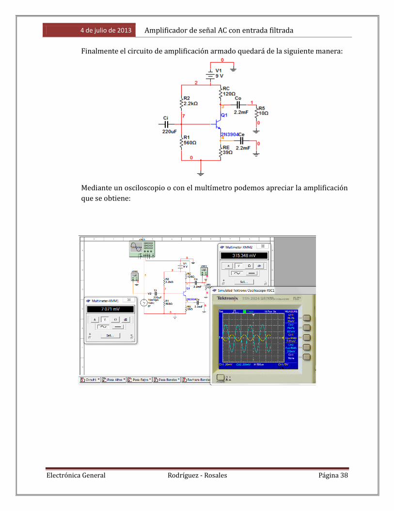
Finalmente el circuito de amplificación armado quedará de la siguiente manera:
Mediante un osciloscopio o con el multímetro podemos apreciar la amplificación
que se obtiene:

4 de julio de 2013 Amplificador de señal AC con entrada filtrada
Electró nica General Ródrí guez - Rósales Pa gina 39
Circuito final:
6. CONCLUSIONES Y RECOMENDACIONES:
Se concluye que:
El transistor trabaja como amplificador de una señal AC bajo cierta
configuración y con los parámetros adecuados, de manera que se puede
accionar actuadores con una señal de entrada pequeña. Materia aplicada del
tercer parcial del presente curso.
Es necesario realizar un correcto filtraje de la señal de salida de audio como
acondicionamiento para su posterior amplificación.

4 de julio de 2013 Amplificador de señal AC con entrada filtrada
Electró nica General Ródrí guez - Rósales Pa gina 40
El acople de impedancia debe realizarse de manera que las corrientes y
voltajes de salida sean apreciables sobre la carga, característica fundamental
y determinante.
La polarización sobre los circuitos de filtraje y amplificación debe ser
apropiada de modo que el requerimiento de energía sea siempre abastecido.
Todos los sub circuitos deben guardar la misma referencia a tierra ya que de
eso depende la correcta entrada o salida de voltajes y corrientes.
Se recomienda:
Obtener el valor de la impedancia de carga antes de realizar el diseño, siendo
esta el dato de partida.
Utilizar filtros de segundo orden o superior. La señal que llegará a los
actuadores será precisa y evidente el rango de frecuencias de trabajo.
Que el arreglo de capacitores sea superior al calculado para que la frecuencia
de acople sea lo menor posible consiguiendo así que el circuito trabaje
siempre en el rango deseado.
7. BIBLIOGRAFÍA:
o Filtrado Rechaza Banda
http://fisica.udea.edu.co/~lab-gicm/Curso%20FPGA_2011/2012_Filtro%20notch.pdf
o Transistor BJT Emisor Común Híbrido. Notas de la clase de electrónica II, Ing. José
Manuel Glez. Rojas
http://lls.ulat.ac.pa/archivos/bquint_9-123-1451/Archivos_de_Cursos/Materia_-_IC-026-
Emisores_y_Receptores_Grupo_-_1_Anio_-_2012-
1/TRANSISTOR_BJT_EMISOR_COMUN_HIBRIDO.pdf

4 de julio de 2013 Amplificador de señal AC con entrada filtrada
Electró nica General Ródrí guez - Rósales Pa gina 41

4 de julio de 2013 Amplificador de señal AC con entrada filtrada
Electró nica General Ródrí guez - Rósales Pa gina 42
IMÁGENES:

4 de julio de 2013 Amplificador de señal AC con entrada filtrada
Electró nica General Ródrí guez - Rósales Pa gina 43

LM158, LM158A, LM258, LM258ALM358, LM358A, LM2904, LM2904VDUAL OPERATIONAL AMPLIFIERS
SLOS068R − JUNE 1976 − REVISED JULY 2010
1POST OFFICE BOX 655303 • DALLAS, TEXAS 75265
Wide Supply Range:− Single Supply . . . 3 V to 32 V
(26 V for LM2904)− or Dual Supplies . . . 1.5 V to 16 V
(13 V for LM2904)
Low Supply-Current Drain, Independent ofSupply Voltage . . . 0.7 mA Typ
Common-Mode Input Voltage RangeIncludes Ground, Allowing Direct SensingNear Ground
Low Input Bias and Offset Parameters:− Input Offset Voltage . . . 3 mV Typ
A Versions . . . 2 mV Typ− Input Offset Current . . . 2 nA Typ− Input Bias Current . . . 20 nA Typ
A Versions . . . 15 nA Typ
Differential Input Voltage Range Equal toMaximum-Rated Supply Voltage . . . 32 V(26 V for LM2904)
Open-Loop Differential VoltageAmplification . . . 100 V/mV Typ
Internal Frequency Compensation
description/ordering information
These devices consist of two independent,high-gain frequency-compensated operationalamplifiers designed to operate from a singlesupply over a wide range of voltages. Operation from split supplies also is possible if the difference betweenthe two supplies is 3 V to 32 V (3 V to 26 V for the LM2904), and VCC is at least 1.5 V more positive than theinput common-mode voltage. The low supply-current drain is independent of the magnitude of the supplyvoltage.
Applications include transducer amplifiers, dc amplification blocks, and all the conventional operationalamplifier circuits that now can be implemented more easily in single-supply-voltage systems. For example,these devices can be operated directly from the standard 5-V supply used in digital systems and easily canprovide the required interface electronics without additional ±5-V supplies.
Please be aware that an important notice concerning availability, standard warranty, and use in critical applications ofTexas Instruments semiconductor products and disclaimers thereto appears at the end of this data sheet.
Copyright 2010, Texas Instruments IncorporatedPRODUCTION DATA information is current as of publication date.Products conform to specifications per the terms of Texas Instrumentsstandard warranty. Production processing does not necessarily includetesting of all parameters.
1
2
3
4
8
7
6
5
1OUT1IN−1IN+GND
VCC2OUT2IN−2IN+
LM158, LM158A . . . JG PACKAGELM258, LM258A . . . D, DGK, OR P PACKAGELM358 . . . D, DGK, P, PS, OR PW PACKAGE
LM358A . . . D, DGK, P, OR PW PACKAGELM2904 . . . D, DGK, P, PS, OR PW PACKAGE
(TOP VIEW)
3 2 1 20 19
9 10 11 12 13
4
5
6
7
8
18
17
16
15
14
NC2OUTNC2IN−NC
NC1IN−
NC1IN+
NC
LM158, LM158A . . . FK PACKAGE(TOP VIEW)
NC
1OU
TN
C
NC
NC
NC
GN
DN
C
CC
+V
2IN
+
NC − No internal connection
On products compliant to MIL-PRF-38535, all parameters are testedunless otherwise noted. On all other products, productionprocessing does not necessarily include testing of all parameters.

LM158, LM158A, LM258, LM258ALM358, LM358A, LM2904, LM2904VDUAL OPERATIONAL AMPLIFIERSSLOS068R − JUNE 1976 − REVISED JULY 2010
2 POST OFFICE BOX 655303 • DALLAS, TEXAS 75265
ORDERING INFORMATION
TAVIOmaxAT 25°C
MAXTESTED
VCC
PACKAGE ORDERABLEPART NUMBER
TOP-SIDEMARKING
PDIP (P) Tube of 50 LM358P LM358P
Tube of 75 LM358D
SOIC (D) Reel of 2500 LM358DR LM358SOIC (D)
Reel of 2500 LM358DRG3
LM358
7 mV 30 V SOP (PS) Reel of 2000 LM358PSR L3587 mV 30 V
Tube of 150 LM358PW
TSSOP (PW) Reel of 2000 LM358PWR L358
0°C to 70°C
TSSOP (PW)
Reel of 2000 LM358PWRG3
L358
0 C to 70 C
MSOP/VSSOP (DGK) Reel of 2500 LM358DGKR M5_§
PDIP (P) Tube of 50 LM358AP LM358AP
SOIC (D)Tube of 75 LM358AD
LM358A
3 mV 30 V
SOIC (D)Reel of 2500 LM358ADR
LM358A
3 mV 30 V
TSSOP (PW)Tube of 150 LM358APW
L358ATSSOP (PW)Reel of 2000 LM358APWR
L358A
MSOP/VSSOP (DGK) Reel of 2500 LM358ADGKR M6_§
PDIP (P) Tube of 50 LM258P LM258P
Tube of 75 LM258D
5 mV 30 V SOIC (D) Reel of 2500 LM258DR LM2585 mV 30 V SOIC (D)
Reel of 2500 LM258DRG3
LM258
−25°C to 85°C MSOP/VSSOP (DGK) Reel of 2500 LM258DGKR M2_§25 C to 85 C
PDIP (P) Tube of 50 LM258AP LM258AP
3 mV 30 V SOIC (D)Tube of 75 LM258AD
LM258A3 mV 30 V SOIC (D)Reel of 2500 LM258ADR
LM258A
MSOP/VSSOP (DGK) Reel of 2500 LM258ADGKR M3_§
PDIP (P) Tube of 50 LM2904P LM2904P
Tube of 75 LM2904D
SOIC (D) Reel of 2500 LM2904DR LM2904SOIC (D)
Reel of 2500 LM2904DRG3
LM2904
7 mV 26 V SOP (PS) Reel of 2000 LM2904PSR L29047 mV 26 V
Tube of 150 LM2904PW
−40°C to 125°C TSSOP (PW) Reel of 2000 LM2904PWR L290440 C to 125 C TSSOP (PW)
Reel of 2000 LM2904PWRG3
L2904
MSOP/VSSOP (DGK) Reel of 2500 LM2904DGKR MB_§
7 mV 32 VSOIC (D) Reel of 2500 LM2904VQDR L2904V
7 mV 32 VTSSOP (PW) Reel of 2000 LM2904VQPWR L2904V
2 mV 32 VSOIC (D) Reel of 2500 LM2904AVQDR L2904AV
2 mV 32 VTSSOP (PW) Reel of 2000 LM2904AVQPWR L2904AV
5 mV 30 VCDIP (JG) Tube of 50 LM158JG LM158JG
55°C to 125°C5 mV 30 V
LCCC (FK) Tube of 55 LM158FK LM158FK−55°C to 125°C
2 mV 30 VCDIP (JG) Tube of 50 LM158AJG LM158AJG
2 mV 30 VLCCC (FK) Tube of 55 LM158AFK LM158AFK
† For the most current package and ordering information, see the Package Option Addendum at the end of this document, or see the TI website at www.ti.com.
‡ Package drawings, thermal data, and symbolization are available at www.ti.com/packaging.

LM158, LM158A, LM258, LM258ALM358, LM358A, LM2904, LM2904VDUAL OPERATIONAL AMPLIFIERS
SLOS068R − JUNE 1976 − REVISED JULY 2010
3POST OFFICE BOX 655303 • DALLAS, TEXAS 75265
§ The actual top-side marking has one additional character that designates the wafer fab/assembly site.

LM158, LM158A, LM258, LM258ALM358, LM358A, LM2904, LM2904VDUAL OPERATIONAL AMPLIFIERSSLOS068R − JUNE 1976 − REVISED JULY 2010
4 POST OFFICE BOX 655303 • DALLAS, TEXAS 75265
symbol (each amplifier)
IN+
IN−OUT+
−
schematic (each amplifier)
VCC+
OUT
GND (or VCC−)
To Other Amplifier
IN−
IN+
≈6-µACurrent
Regulator
≈6-µACurrent
Regulator
≈100-µACurrent
Regulator
≈50-µACurrent
Regulator
Epi-FETDiodesResistorsTransistorsCapacitors
COMPONENT COUNT
127512

LM158, LM158A, LM258, LM258ALM358, LM358A, LM2904, LM2904VDUAL OPERATIONAL AMPLIFIERS
SLOS068R − JUNE 1976 − REVISED JULY 2010
5POST OFFICE BOX 655303 • DALLAS, TEXAS 75265
absolute maximum ratings over operating free-air temperature range (unless otherwise noted)†
LM158, LM158ALM258, LM258ALM358, LM358A
LM2904V
LM2904 UNIT
Supply voltage, VCC (see Note 1) ±16 or 32 ±13 or 26 V
Differential input voltage, VID (see Note 2) ±32 ±26 V
Input voltage, VI (either input) −0.3 to 32 −0.3 to 26 V
Duration of output short circuit (one amplifier) to groundat (or below) 25°C free-air temperature (VCC ≤ 15 V) (see Note 3)
Unlimited Unlimited
D package 97 97
DGK package 172 172
Package thermal impedance, JA (see Notes 4 and 5) P package 85 85 °C/WPackage thermal impedance, JA (see Notes 4 and 5)
PS package 95 95
C/W
PW package 149 149
Package thermal impedance (see Notes 6 and 7)FK package 5.61
°C/WPackage thermal impedance, JC (see Notes 6 and 7)JG package 14.5
°C/W
LM158, LM158A −55 to 125
Operating free air temperature range TLM258, LM258A −25 to 85
°COperating free-air temperature range, TA LM358, LM358A 0 to 70°C
LM2904 −40 to 125 −40 to 125
Operating virtual junction temperature, TJ 150 150 °C
Case temperature for 60 seconds FK package 260 °C
Lead temperature 1,6 mm (1/16 inch) from case for 60 seconds JG package 300 300 °C
Storage temperature range, Tstg −65 to 150 −65 to 150 °C† Stresses beyond those listed under “absolute maximum ratings” may cause permanent damage to the device. These are stress ratings only, and
functional operation of the device at these or any other conditions beyond those indicated under “recommended operating conditions” is notimplied. Exposure to absolute-maximum-rated conditions for extended periods may affect device reliability.
NOTES: 1. All voltage values, except differential voltages and VCC specified for measurement of IOS, are with respect to the network groundterminal.
2. Differential voltages are at IN+ with respect to IN−.3. Short circuits from outputs to VCC can cause excessive heating and eventual destruction.4. Maximum power dissipation is a function of TJ(max), JA, and TA. The maximum allowable power dissipation at any allowable
ambient temperature is PD = (TJ(max) − TA)/JA. Operating at the absolute maximum TJ of 150°C can affect reliability.5. The package thermal impedance is calculated in accordance with JESD 51-7.6. Maximum power dissipation is a function of TJ(max), JC, and TC. The maximum allowable power dissipation at any allowable case
temperature is PD = (TJ(max) − TC)/JC. Operating at the absolute maximum TJ of 150°C can affect reliability.7. The package thermal impedance is calculated in accordance with MIL-STD-883.
LM158, LM158A, LM258, LM258ALM358, LM358A, LM2904, LM2904VDUAL OPERATIONAL AMPLIFIERSSLOS068R − JUNE 1976 − REVISED JULY 2010
6 POST OFFICE BOX 655303 • DALLAS, TEXAS 75265
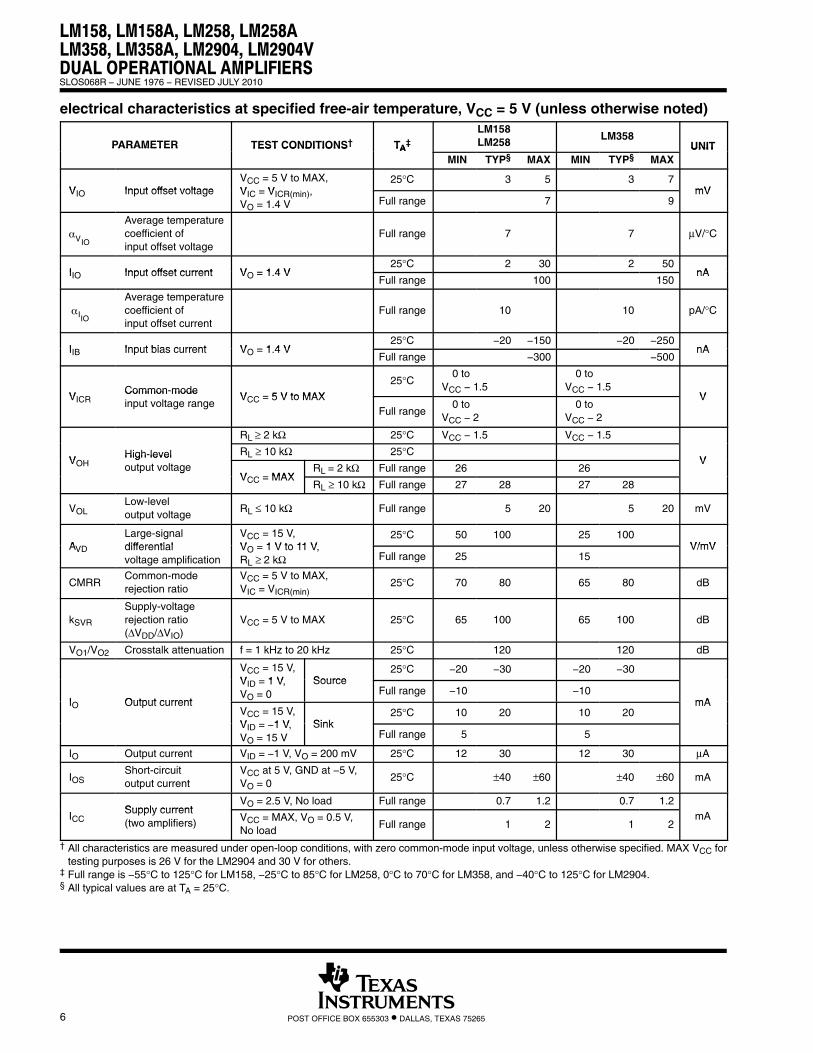
electrical characteristics at specified free-air temperature, VCC = 5 V (unless otherwise noted)
PARAMETER TEST CONDITIONS† TA‡
LM158LM258 LM358
UNITPARAMETER TEST CONDITIONS TAMIN TYP§ MAX MIN TYP§ MAX
UNIT
V Input offset voltageVCC = 5 V to MAX,V V
25°C 3 5 3 7mVVIO Input offset voltage VIC = VICR(min),
VO = 1.4 V Full range 7 9mV
VIO
Average temperaturecoefficient ofinput offset voltage
Full range 7 7 µV/°C
I Input offset current V = 1 4 V25°C 2 30 2 50
nAIIO Input offset current VO = 1.4 VFull range 100 150
nA
IIO
Average temperaturecoefficient ofinput offset current
Full range 10 10 pA/°C
I Input bias current V = 1 4 V25°C −20 −150 −20 −250
nAIIB Input bias current VO = 1.4 VFull range −300 −500
nA
V CCommon-mode
VCC = 5 V to MAX
25°C0 to
VCC − 1.50 to
VCC − 1.5VVICR
Common modeinput voltage range
VCC = 5 V to MAXFull range
0 toVCC − 2
0 toVCC − 2
V
RL ≥ 2 kΩ 25°C VCC − 1.5 VCC − 1.5
VHigh-level RL ≥ 10 kΩ 25°C
VVOHHigh leveloutput voltage
V = MAXRL = 2 kΩ Full range 26 26
Vp g
VCC = MAXRL ≥ 10 kΩ Full range 27 28 27 28
VOLLow-leveloutput voltage
RL ≤ 10 kΩ Full range 5 20 5 20 mV
ALarge-signaldifferential
VCC = 15 V, V 1 V to 11 V
25°C 50 100 25 100V/mVAVD differential
voltage amplificationVO = 1 V to 11 V,RL ≥ 2 kΩ Full range 25 15
V/mV
CMRRCommon-moderejection ratio
VCC = 5 V to MAX,VIC = VICR(min)
25°C 70 80 65 80 dB
kSVR
Supply-voltagerejection ratio(∆VDD/∆VIO)
VCC = 5 V to MAX 25°C 65 100 65 100 dB
VO1/VO2 Crosstalk attenuation f = 1 kHz to 20 kHz 25°C 120 120 dB
VCC = 15 V,V 1 V Source
25°C −20 −30 −20 −30
I Output current
VID = 1 V,VO = 0
SourceFull range −10 −10
mAIO Output currentVCC = 15 V,V 1 V Sink
25°C 10 20 10 20mA
VID = −1 V,VO = 15 V
SinkFull range 5 5
IO Output current VID = −1 V, VO = 200 mV 25°C 12 30 12 30 µA
IOSShort-circuitoutput current
VCC at 5 V, GND at −5 V,VO = 0
25°C ±40 ±60 ±40 ±60 mA
Supply currentVO = 2.5 V, No load Full range 0.7 1.2 0.7 1.2
ICCSupply current(two amplifiers) VCC = MAX, VO = 0.5 V,
No loadFull range 1 2 1 2
mA
† All characteristics are measured under open-loop conditions, with zero common-mode input voltage, unless otherwise specified. MAX VCC fortesting purposes is 26 V for the LM2904 and 30 V for others.
‡ Full range is −55°C to 125°C for LM158, −25°C to 85°C for LM258, 0°C to 70°C for LM358, and −40°C to 125°C for LM2904.§ All typical values are at TA = 25°C.
LM158, LM158A, LM258, LM258ALM358, LM358A, LM2904, LM2904VDUAL OPERATIONAL AMPLIFIERS
SLOS068R − JUNE 1976 − REVISED JULY 2010
7POST OFFICE BOX 655303 • DALLAS, TEXAS 75265
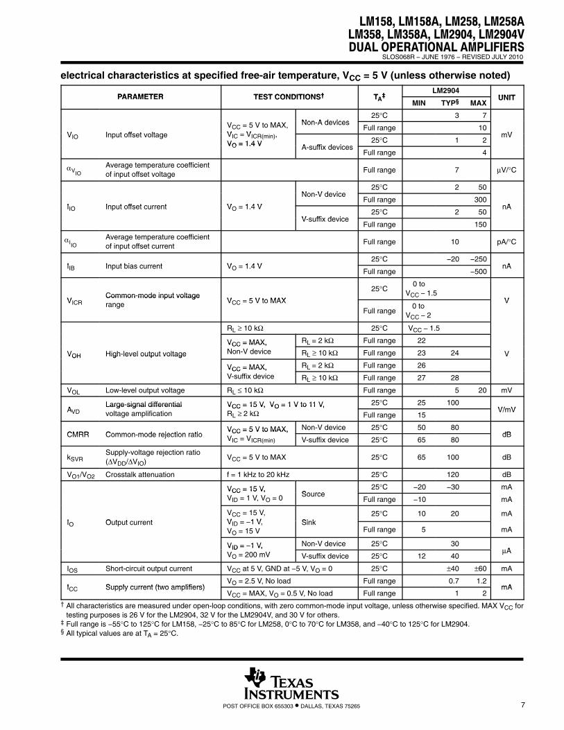
electrical characteristics at specified free-air temperature, VCC = 5 V (unless otherwise noted)
PARAMETER TEST CONDITIONS† T ‡LM2904
UNITPARAMETER TEST CONDITIONS† TA‡
MIN TYP§ MAXUNIT
Non A devices25°C 3 7
V Input offset voltageVCC = 5 V to MAX,V V
Non-A devicesFull range 10
mVVIO Input offset voltage VIC = VICR(min), VO = 1.4 V A suffix devices
25°C 1 2mV
VO = 1.4 V A-suffix devicesFull range 4
VIOAverage temperature coefficientof input offset voltage
Full range 7 µV/°C
Non V device25°C 2 50
I Input offset current V 1 4 V
Non-V deviceFull range 300
nAIIO Input offset current VO = 1.4 V
V suffix device25°C 2 50
nA
V-suffix deviceFull range 150
IIOAverage temperature coefficientof input offset current
Full range 10 pA/°C
I Input bias current V 1 4 V25°C −20 −250
nAIIB Input bias current VO = 1.4 VFull range −500
nA
VCommon-mode input voltage
V 5 V to MAX
25°C0 to
VCC − 1.5VVICR
Common mode input voltagerange VCC = 5 V to MAX
Full range0 to
VCC − 2
V
RL ≥ 10 kΩ 25°C VCC − 1.5
VCC = MAX, RL = 2 kΩ Full range 22
VOH High-level output voltage
VCC = MAX,Non-V device RL ≥ 10 kΩ Full range 23 24 VVOH High level output voltage
VCC = MAX, RL = 2 kΩ Full range 26
V
VCC = MAX,V-suffix device RL ≥ 10 kΩ Full range 27 28
VOL Low-level output voltage RL ≤ 10 kΩ Full range 5 20 mV
ALarge-signal differential VCC = 15 V, VO = 1 V to 11 V, 25°C 25 100
V/mVAVDLarge signal differentialvoltage amplification
VCC = 15 V, VO = 1 V to 11 V,RL ≥ 2 kΩ Full range 15
V/mV
CMRR Common mode rejection ratioVCC = 5 V to MAX, Non-V device 25°C 50 80
dBCMRR Common-mode rejection ratioVCC = 5 V to MAX,VIC = VICR(min) V-suffix device 25°C 65 80
dB
kSVRSupply-voltage rejection ratio(∆VDD/∆VIO)
VCC = 5 V to MAX 25°C 65 100 dB
VO1/VO2 Crosstalk attenuation f = 1 kHz to 20 kHz 25°C 120 dB
VCC = 15 V,Source
25°C −20 −30 mAVCC = 15 V,VID = 1 V, VO = 0 Source
Full range −10 mA
I Output currentVCC = 15 V,V 1 V Sink
25°C 10 20 mAIO Output current VID = −1 V,
VO = 15 VSink
Full range 5 mA
VID = −1 V, Non-V device 25°C 30A
VID = 1 V,VO = 200 mV V-suffix device 25°C 12 40
µA
IOS Short-circuit output current VCC at 5 V, GND at −5 V, VO = 0 25°C ±40 ±60 mA
ICC Supply current (two amplifiers)VO = 2.5 V, No load Full range 0.7 1.2
mAICC Supply current (two amplifiers)VCC = MAX, VO = 0.5 V, No load Full range 1 2
mA
† All characteristics are measured under open-loop conditions, with zero common-mode input voltage, unless otherwise specified. MAX VCC fortesting purposes is 26 V for the LM2904, 32 V for the LM2904V, and 30 V for others.
‡ Full range is −55°C to 125°C for LM158, −25°C to 85°C for LM258, 0°C to 70°C for LM358, and −40°C to 125°C for LM2904.§ All typical values are at TA = 25°C.

LM158, LM158A, LM258, LM258ALM358, LM358A, LM2904, LM2904VDUAL OPERATIONAL AMPLIFIERSSLOS068R − JUNE 1976 − REVISED JULY 2010
8 POST OFFICE BOX 655303 • DALLAS, TEXAS 75265
electrical characteristics at specified free-air temperature, VCC = 5 V (unless otherwise noted)
PARAMETER TEST CONDITIONS† T ‡LM158A LM258A
UNITPARAMETER TEST CONDITIONS† TA‡
MIN TYP§ MAX MIN TYP§ MAXUNIT
V Input offset voltageVCC = 5 V to 30 V,V V
25°C 2 2 3mVVIO Input offset voltage VIC = VICR(min),
VO = 1.4 V Full range 4 4mV
VIO
Averagetemperaturecoefficient ofinput offset voltage
Full range 7 15* 7 15 µV/°C
I Input offset current V = 1 4 V25°C 2 10 2 15
nAIIO Input offset current VO = 1.4 VFull range 30 30
nA
IIO
Averagetemperaturecoefficient ofinput offset current
Full range 10 200 10 200 pA/°C
I Input bias current V = 1 4 V25°C −15 −50 −15 −80
nAIIB Input bias current VO = 1.4 VFull range −100 −100
nA
V CCommon-mode
VCC = 30 V
25°C0 to
VCC − 1.50 to
VCC − 1.5VVICR
Common modeinput voltage range
VCC = 30 VFull range
0 toVCC − 2
0 toVCC − 2
V
High levelRL ≥ 2 kΩ 25°C VCC − 1.5 VCC − 1.5
VOHHigh-leveloutput voltage V = 30 V
RL = 2 kΩ Full range 26 26 VVOH output voltage VCC = 30 VRL ≥ 10 kΩ Full range 27 28 27 28
V
VOLLow-leveloutput voltage
RL ≤ 10 kΩ Full range 5 20 5 20 mV
ALarge-signaldifferential
VCC = 15 V,V 1 V to 11 V
25°C 50 100 50 100V/mVAVD differential
voltage amplificationVO = 1 V to 11 V,RL ≥ 2 kΩ Full range 25 25
V/mV
CMRRCommon-moderejection ratio
25°C 70 80 70 80 dB
kSVR
Supply-voltagerejection ratio(∆VDD/∆VIO)
25°C 65 100 65 100 dB
VO1/VO2Crosstalkattenuation
f = 1 kHz to 20 kHz 25°C 120 120 dB
VCC = 15 V,V 1 V Source
25°C −20 −30 −60 −20 −30 −60VID = 1 V,VO = 0
SourceFull range −10 −10
mAIO Output current VCC = 15 V,
V 1 V Sink25°C 10 20 10 20
mA
VID = −1 V,VO = 15
SinkFull range 5 5
VID = −1 V, VO = 200 mV 25°C 12 30 12 30 µA
IOSShort-circuit outputcurrent
VCC at 5 V, GND at −5 V,VO = 0
25°C ±40 ±60 ±40 ±60 mA
Supply current (twoVO = 2.5 V, No load Full range 0.7 1.2 0.7 1.2
ICCSupply current (twoamplifiers) VCC = MAX, VO = 0.5 V,
No loadFull range 1 2 1 2
mA
*On products compliant to MIL-PRF-38535, this parameter is not production tested.† All characteristics are measured under open-loop conditions, with zero common-mode input voltage, unless otherwise specified. MAX VCC for
testing purposes is 26 V for LM2904 and 30 V for others.‡ Full range is −55°C to 125°C for LM158A, −25°C to 85°C for LM258A, and 0°C to 70°C for LM358A.§ All typical values are at TA = 25°C.

LM158, LM158A, LM258, LM258ALM358, LM358A, LM2904, LM2904VDUAL OPERATIONAL AMPLIFIERS
SLOS068R − JUNE 1976 − REVISED JULY 2010
9POST OFFICE BOX 655303 • DALLAS, TEXAS 75265
electrical characteristics at specified free-air temperature, VCC = 5 V (unless otherwise noted)
PARAMETER TEST CONDITIONS† T ‡LM358A
UNITPARAMETER TEST CONDITIONS† TA‡
MIN TYP§ MAXUNIT
V Input offset voltageVCC = 5 V to 30 V, 25°C 2 3
mVVIO Input offset voltageVCC = 5 V to 30 V,VIC = VICR(min), VO = 1.4 V Full range 5
mV
VIOAverage temperature coefficient ofinput offset voltage
Full range 7 20 µV/°C
I Input offset current V 1 4 V25°C 2 30
nAIIO Input offset current VO = 1.4 VFull range 75
nA
IIOAverage temperature coefficient ofinput offset current
Full range 10 300 pA/°C
I Input bias current V 1 4 V25°C −15 −100
nAIIB Input bias current VO = 1.4 VFull range −200
nA
V Common mode input voltage range V 30 V
25°C0 to
VCC − 1.5VVICR Common-mode input voltage range VCC = 30 V
Full range0 to
VCC − 2
V
RL ≥ 2 kΩ 25°C VCC − 1.5
VOH High-level output voltageV 30 V
RL = 2 kΩ Full range 26 VVOH High level output voltageVCC = 30 V
RL ≥ 10 kΩ Full range 27 28
V
VOL Low-level output voltage RL ≤ 10 kΩ Full range 5 20 mV
ALarge-signal differential VCC = 15 V, VO = 1 V to 11 V, 25°C 25 100
V/mVAVDLarge signal differentialvoltage amplification
VCC = 15 V, VO = 1 V to 11 V,RL ≥ 2 kΩ Full range 15
V/mV
CMRR Common-mode rejection ratio 25°C 65 80 dB
kSVRSupply-voltage rejection ratio(∆VDD/∆VIO)
25°C 65 100 dB
VO1/VO2 Crosstalk attenuation f = 1 kHz to 20 kHz 25°C 120 dB
VCC = 15 V,V 1 V Source
25°C −20 −30 −60VID = 1 V,VO = 0
SourceFull range −10
mAIO Output current VCC = 15 V,
V 1 V Sink25°C 10 20
mA
VID = −1 V,VO = 15 V
SinkFull range 5
VID = −1 V, VO = 200 mV 25°C 30 µA
IOS Short-circuit output current VCC at 5 V, GND at −5 V, VO = 0 25°C ±40 ±60 mA
I Supply current (two amplifiers)VO = 2.5 V, No load Full range 0.7 1.2
mAICC Supply current (two amplifiers)VCC = MAX, VO = 0.5 V, No load Full range 1 2
mA
† All characteristics are measured under open-loop conditions, with zero common-mode input voltage, unless otherwise specified. MAX VCC fortesting purposes is 26 V for LM2904 and 30 V for others.
‡ Full range is −55°C to 125°C for LM158A, −25°C to 85°C for LM258A, and 0°C to 70°C for LM358A.§ All typical values are at TA = 25°C.

LM158, LM158A, LM258, LM258ALM358, LM358A, LM2904, LM2904VDUAL OPERATIONAL AMPLIFIERSSLOS068R − JUNE 1976 − REVISED JULY 2010
10 POST OFFICE BOX 655303 • DALLAS, TEXAS 75265
operating conditions, VCC = ±15 V, TA = 25°CPARAMETER TEST CONDITIONS TYP UNIT
SR Slew rate at unity gainRL = 1 MΩ, CL = 30 pF, VI = ±10 V(see Figure 1)
0.3 V/µs
B1 Unity-gain bandwidth RL = 1 MΩ, CL = 20 pF (see Figure 1) 0.7 MHz
Vn Equivalent input noise voltageRS = 100 Ω, VI = 0 V, f = 1 kHz(see Figure 2)
40 nV/√Hz
+VO
−
RLCL
VI
VCC+
VCC−
Figure 1. Unity-Gain Amplifier
−
+VO
100 ΩVCC+
VCC−
RS
900 Ω
VI = 0 V
Figure 2. Noise-Test Circuit

PACKAGE OPTION ADDENDUM
www.ti.com 11-Apr-2013
Addendum-Page 1
PACKAGING INFORMATION
Orderable Device Status(1)
Package Type PackageDrawing
Pins PackageQty
Eco Plan(2)
Lead/Ball Finish MSL Peak Temp(3)
Op Temp (°C) Top-Side Markings(4)
Samples
5962-87710012A ACTIVE LCCC FK 20 1 TBD Call TI Call TI -55 to 125 5962-87710012ALM158FKB
5962-8771001PA ACTIVE CDIP JG 8 1 TBD Call TI Call TI -55 to 125 8771001PALM158
5962-87710022A ACTIVE LCCC FK 20 1 TBD Call TI Call TI -55 to 125 5962-87710022ALM158AFKB
5962-8771002PA ACTIVE CDIP JG 8 1 TBD Call TI Call TI -55 to 125 8771002PALM158A
LM158AFKB ACTIVE LCCC FK 20 1 TBD POST-PLATE N / A for Pkg Type -55 to 125 5962-87710022ALM158AFKB
LM158AJG ACTIVE CDIP JG 8 1 TBD A42 N / A for Pkg Type -55 to 125 LM158AJG
LM158AJGB ACTIVE CDIP JG 8 1 TBD A42 N / A for Pkg Type -55 to 125 8771002PALM158A
LM158FKB ACTIVE LCCC FK 20 1 TBD POST-PLATE N / A for Pkg Type -55 to 125 5962-87710012ALM158FKB
LM158JG ACTIVE CDIP JG 8 1 TBD A42 N / A for Pkg Type -55 to 125 LM158JG
LM158JGB ACTIVE CDIP JG 8 1 TBD A42 N / A for Pkg Type -55 to 125 8771001PALM158
LM258AD ACTIVE SOIC D 8 75 Green (RoHS& no Sb/Br)
CU NIPDAU Level-1-260C-UNLIM -25 to 85 LM258A
LM258ADE4 ACTIVE SOIC D 8 75 Green (RoHS& no Sb/Br)
CU NIPDAU Level-1-260C-UNLIM -25 to 85 LM258A
LM258ADG4 ACTIVE SOIC D 8 75 Green (RoHS& no Sb/Br)
CU NIPDAU Level-1-260C-UNLIM -25 to 85 LM258A
LM258ADGKR ACTIVE VSSOP DGK 8 2500 Green (RoHS& no Sb/Br)
CU NIPDAU Level-1-260C-UNLIM -25 to 85 (M3L ~ M3P ~ M3S ~ M3U)
LM258ADGKRG4 ACTIVE VSSOP DGK 8 2500 Green (RoHS& no Sb/Br)
CU NIPDAU Level-1-260C-UNLIM -25 to 85 (M3L ~ M3P ~ M3S ~ M3U)
LM258ADR ACTIVE SOIC D 8 2500 Green (RoHS& no Sb/Br)
CU NIPDAU Level-1-260C-UNLIM -25 to 85 LM258A

PACKAGE OPTION ADDENDUM
www.ti.com 11-Apr-2013
Addendum-Page 2
Orderable Device Status(1)
Package Type PackageDrawing
Pins PackageQty
Eco Plan(2)
Lead/Ball Finish MSL Peak Temp(3)
Op Temp (°C) Top-Side Markings(4)
Samples
LM258ADRE4 ACTIVE SOIC D 8 2500 Green (RoHS& no Sb/Br)
CU NIPDAU Level-1-260C-UNLIM -25 to 85 LM258A
LM258ADRG4 ACTIVE SOIC D 8 2500 Green (RoHS& no Sb/Br)
CU NIPDAU Level-1-260C-UNLIM -25 to 85 LM258A
LM258AP ACTIVE PDIP P 8 50 Pb-Free(RoHS)
CU NIPDAU N / A for Pkg Type -25 to 85 LM258AP
LM258APE4 ACTIVE PDIP P 8 50 Pb-Free(RoHS)
CU NIPDAU N / A for Pkg Type -25 to 85 LM258AP
LM258D ACTIVE SOIC D 8 75 Green (RoHS& no Sb/Br)
CU NIPDAU Level-1-260C-UNLIM -25 to 85 LM258
LM258DE4 ACTIVE SOIC D 8 75 Green (RoHS& no Sb/Br)
CU NIPDAU Level-1-260C-UNLIM -25 to 85 LM258
LM258DG4 ACTIVE SOIC D 8 75 Green (RoHS& no Sb/Br)
CU NIPDAU Level-1-260C-UNLIM -25 to 85 LM258
LM258DGKR ACTIVE VSSOP DGK 8 2500 Green (RoHS& no Sb/Br)
CU NIPDAU Level-1-260C-UNLIM -25 to 85 (M2L ~ M2P ~ M2S ~ M2U)
LM258DGKRG4 ACTIVE VSSOP DGK 8 2500 Green (RoHS& no Sb/Br)
CU NIPDAU Level-1-260C-UNLIM -25 to 85 (M2L ~ M2P ~ M2S ~ M2U)
LM258DR ACTIVE SOIC D 8 2500 Green (RoHS& no Sb/Br)
CU NIPDAU Level-1-260C-UNLIM -25 to 85 LM258
LM258DRE4 ACTIVE SOIC D 8 Green (RoHS& no Sb/Br)
CU NIPDAU Level-1-260C-UNLIM -25 to 85 LM258
LM258DRG3 ACTIVE SOIC D 8 2500 Green (RoHS& no Sb/Br)
CU SN Level-1-260C-UNLIM -25 to 85 LM258
LM258DRG4 ACTIVE SOIC D 8 2500 Green (RoHS& no Sb/Br)
CU NIPDAU Level-1-260C-UNLIM -25 to 85 LM258
LM258P ACTIVE PDIP P 8 50 Pb-Free(RoHS)
CU NIPDAU N / A for Pkg Type -25 to 85 LM258P
LM258PE4 ACTIVE PDIP P 8 50 Pb-Free(RoHS)
CU NIPDAU N / A for Pkg Type -25 to 85 LM258P
LM2904AVQDR ACTIVE SOIC D 8 2500 Green (RoHS& no Sb/Br)
CU NIPDAU Level-1-260C-UNLIM -40 to 125 L2904AV
LM2904AVQDRG4 ACTIVE SOIC D 8 2500 Green (RoHS& no Sb/Br)
CU NIPDAU Level-1-260C-UNLIM -40 to 125 L2904AV
LM2904AVQPWR ACTIVE TSSOP PW 8 2000 Green (RoHS& no Sb/Br)
CU NIPDAU Level-1-260C-UNLIM -40 to 125 L2904AV

PACKAGE OPTION ADDENDUM
www.ti.com 11-Apr-2013
Addendum-Page 3
Orderable Device Status(1)
Package Type PackageDrawing
Pins PackageQty
Eco Plan(2)
Lead/Ball Finish MSL Peak Temp(3)
Op Temp (°C) Top-Side Markings(4)
Samples
LM2904AVQPWRG4 ACTIVE TSSOP PW 8 2000 Green (RoHS& no Sb/Br)
CU NIPDAU Level-1-260C-UNLIM -40 to 125 L2904AV
LM2904D ACTIVE SOIC D 8 75 Green (RoHS& no Sb/Br)
CU NIPDAU Level-1-260C-UNLIM -40 to 125 LM2904
LM2904DE4 ACTIVE SOIC D 8 75 Green (RoHS& no Sb/Br)
CU NIPDAU Level-1-260C-UNLIM -40 to 125 LM2904
LM2904DG4 ACTIVE SOIC D 8 75 Green (RoHS& no Sb/Br)
CU NIPDAU Level-1-260C-UNLIM -40 to 125 LM2904
LM2904DGKR ACTIVE VSSOP DGK 8 2500 Green (RoHS& no Sb/Br)
CU NIPDAU Level-1-260C-UNLIM -40 to 125 (MBL ~ MBP ~ MBS ~ MBU)
LM2904DGKRG4 ACTIVE VSSOP DGK 8 2500 Green (RoHS& no Sb/Br)
CU NIPDAU Level-1-260C-UNLIM -40 to 125 (MBL ~ MBP ~ MBS ~ MBU)
LM2904DR ACTIVE SOIC D 8 2500 Green (RoHS& no Sb/Br)
CU NIPDAU Level-1-260C-UNLIM -40 to 125 LM2904
LM2904DRE4 ACTIVE SOIC D 8 2500 Green (RoHS& no Sb/Br)
CU NIPDAU Level-1-260C-UNLIM -40 to 125 LM2904
LM2904DRG3 ACTIVE SOIC D 8 2500 Green (RoHS& no Sb/Br)
CU SN Level-1-260C-UNLIM -40 to 125 LM2904
LM2904DRG4 ACTIVE SOIC D 8 2500 Green (RoHS& no Sb/Br)
CU NIPDAU Level-1-260C-UNLIM -40 to 125 LM2904
LM2904P ACTIVE PDIP P 8 50 Pb-Free(RoHS)
CU NIPDAU N / A for Pkg Type -40 to 125 LM2904P
LM2904PE4 ACTIVE PDIP P 8 50 Pb-Free(RoHS)
CU NIPDAU N / A for Pkg Type -40 to 125 LM2904P
LM2904PSR ACTIVE SO PS 8 2000 Green (RoHS& no Sb/Br)
CU NIPDAU Level-1-260C-UNLIM -40 to 125 L2904
LM2904PSRE4 ACTIVE SO PS 8 2000 Green (RoHS& no Sb/Br)
CU NIPDAU Level-1-260C-UNLIM -40 to 125 L2904
LM2904PSRG4 ACTIVE SO PS 8 2000 Green (RoHS& no Sb/Br)
CU NIPDAU Level-1-260C-UNLIM -40 to 125 L2904
LM2904PW ACTIVE TSSOP PW 8 150 Green (RoHS& no Sb/Br)
CU NIPDAU Level-1-260C-UNLIM -40 to 125 L2904
LM2904PWE4 ACTIVE TSSOP PW 8 150 Green (RoHS& no Sb/Br)
CU NIPDAU Level-1-260C-UNLIM -40 to 125 L2904
LM2904PWG4 ACTIVE TSSOP PW 8 150 Green (RoHS& no Sb/Br)
CU NIPDAU Level-1-260C-UNLIM -40 to 125 L2904

PACKAGE OPTION ADDENDUM
www.ti.com 11-Apr-2013
Addendum-Page 4
Orderable Device Status(1)
Package Type PackageDrawing
Pins PackageQty
Eco Plan(2)
Lead/Ball Finish MSL Peak Temp(3)
Op Temp (°C) Top-Side Markings(4)
Samples
LM2904PWLE OBSOLETE TSSOP PW 8 TBD Call TI Call TI -40 to 125
LM2904PWR ACTIVE TSSOP PW 8 2000 Green (RoHS& no Sb/Br)
CU NIPDAU Level-1-260C-UNLIM -40 to 125 L2904
LM2904PWRG3 ACTIVE TSSOP PW 8 2000 Green (RoHS& no Sb/Br)
CU SN Level-1-260C-UNLIM -40 to 125 L2904
LM2904QD OBSOLETE SOIC D 8 TBD Call TI Call TI -40 to 125
LM2904QDR ACTIVE SOIC D 8 2500 Green (RoHS& no Sb/Br)
CU NIPDAU Level-1-260C-UNLIM -40 to 125 2904Q1
LM2904QDRG4 ACTIVE SOIC D 8 2500 Green (RoHS& no Sb/Br)
CU NIPDAU Level-1-260C-UNLIM -40 to 125 2904Q1
LM2904QP OBSOLETE PDIP P 8 TBD Call TI Call TI -40 to 125
LM2904VQDR ACTIVE SOIC D 8 2500 Green (RoHS& no Sb/Br)
CU NIPDAU Level-1-260C-UNLIM -40 to 125 L2904V
LM2904VQDRG4 ACTIVE SOIC D 8 2500 Green (RoHS& no Sb/Br)
CU NIPDAU Level-1-260C-UNLIM -40 to 125 L2904V
LM2904VQPWR ACTIVE TSSOP PW 8 2000 Green (RoHS& no Sb/Br)
CU NIPDAU Level-1-260C-UNLIM -40 to 125 L2904V
LM2904VQPWRG4 ACTIVE TSSOP PW 8 2000 Green (RoHS& no Sb/Br)
CU NIPDAU Level-1-260C-UNLIM -40 to 125 L2904V
LM358AD ACTIVE SOIC D 8 75 Green (RoHS& no Sb/Br)
CU NIPDAU Level-1-260C-UNLIM 0 to 70 LM358A
LM358ADE4 ACTIVE SOIC D 8 75 Green (RoHS& no Sb/Br)
CU NIPDAU Level-1-260C-UNLIM 0 to 70 LM358A
LM358ADG4 ACTIVE SOIC D 8 75 Green (RoHS& no Sb/Br)
CU NIPDAU Level-1-260C-UNLIM 0 to 70 LM358A
LM358ADGKR ACTIVE VSSOP DGK 8 2500 Green (RoHS& no Sb/Br)
CU NIPDAU Level-1-260C-UNLIM 0 to 70 (M6L ~ M6P ~ M6S ~ M6U)
LM358ADGKRG4 ACTIVE VSSOP DGK 8 2500 Green (RoHS& no Sb/Br)
CU NIPDAU Level-1-260C-UNLIM 0 to 70 (M6L ~ M6P ~ M6S ~ M6U)
LM358ADR ACTIVE SOIC D 8 2500 Green (RoHS& no Sb/Br)
CU NIPDAU Level-1-260C-UNLIM 0 to 70 LM358A
LM358ADRE4 ACTIVE SOIC D 8 2500 Green (RoHS& no Sb/Br)
CU NIPDAU Level-1-260C-UNLIM 0 to 70 LM358A
LM358ADRG4 ACTIVE SOIC D 8 2500 Green (RoHS& no Sb/Br)
CU NIPDAU Level-1-260C-UNLIM 0 to 70 LM358A

PACKAGE OPTION ADDENDUM
www.ti.com 11-Apr-2013
Addendum-Page 5
Orderable Device Status(1)
Package Type PackageDrawing
Pins PackageQty
Eco Plan(2)
Lead/Ball Finish MSL Peak Temp(3)
Op Temp (°C) Top-Side Markings(4)
Samples
LM358AP ACTIVE PDIP P 8 50 Pb-Free(RoHS)
CU NIPDAU N / A for Pkg Type 0 to 70 LM358AP
LM358APE4 ACTIVE PDIP P 8 50 Pb-Free(RoHS)
CU NIPDAU N / A for Pkg Type 0 to 70 LM358AP
LM358APW ACTIVE TSSOP PW 8 150 Green (RoHS& no Sb/Br)
CU NIPDAU Level-1-260C-UNLIM 0 to 70 L358A
LM358APWE4 ACTIVE TSSOP PW 8 150 Green (RoHS& no Sb/Br)
CU NIPDAU Level-1-260C-UNLIM 0 to 70 L358A
LM358APWG4 ACTIVE TSSOP PW 8 150 Green (RoHS& no Sb/Br)
CU NIPDAU Level-1-260C-UNLIM 0 to 70 L358A
LM358APWR ACTIVE TSSOP PW 8 2000 Green (RoHS& no Sb/Br)
CU NIPDAU Level-1-260C-UNLIM 0 to 70 L358A
LM358APWRE4 ACTIVE TSSOP PW 8 2000 Green (RoHS& no Sb/Br)
CU NIPDAU Level-1-260C-UNLIM 0 to 70 L358A
LM358APWRG4 ACTIVE TSSOP PW 8 2000 Green (RoHS& no Sb/Br)
CU NIPDAU Level-1-260C-UNLIM 0 to 70 L358A
LM358D ACTIVE SOIC D 8 75 Green (RoHS& no Sb/Br)
CU NIPDAU Level-1-260C-UNLIM 0 to 70 LM358
LM358DE4 ACTIVE SOIC D 8 75 Green (RoHS& no Sb/Br)
CU NIPDAU Level-1-260C-UNLIM 0 to 70 LM358
LM358DG4 ACTIVE SOIC D 8 75 Green (RoHS& no Sb/Br)
CU NIPDAU Level-1-260C-UNLIM 0 to 70 LM358
LM358DGKR ACTIVE VSSOP DGK 8 2500 Green (RoHS& no Sb/Br)
CU NIPDAU Level-1-260C-UNLIM 0 to 70 (M5L ~ M5P ~ M5S ~ M5U)
LM358DGKRG4 ACTIVE VSSOP DGK 8 2500 Green (RoHS& no Sb/Br)
CU NIPDAU Level-1-260C-UNLIM 0 to 70 (M5L ~ M5P ~ M5S ~ M5U)
LM358DR ACTIVE SOIC D 8 2500 Green (RoHS& no Sb/Br)
CU NIPDAU Level-1-260C-UNLIM 0 to 70 LM358
LM358DRE4 ACTIVE SOIC D 8 2500 Green (RoHS& no Sb/Br)
CU NIPDAU Level-1-260C-UNLIM 0 to 70 LM358
LM358DRG3 ACTIVE SOIC D 8 2500 Green (RoHS& no Sb/Br)
CU SN Level-1-260C-UNLIM 0 to 70 LM358
LM358DRG4 ACTIVE SOIC D 8 2500 Green (RoHS& no Sb/Br)
CU NIPDAU Level-1-260C-UNLIM 0 to 70 LM358
LM358P ACTIVE PDIP P 8 50 Pb-Free(RoHS)
CU NIPDAU N / A for Pkg Type 0 to 70 LM358P

PACKAGE OPTION ADDENDUM
www.ti.com 11-Apr-2013
Addendum-Page 6
Orderable Device Status(1)
Package Type PackageDrawing
Pins PackageQty
Eco Plan(2)
Lead/Ball Finish MSL Peak Temp(3)
Op Temp (°C) Top-Side Markings(4)
Samples
LM358PE3 ACTIVE PDIP P 8 50 Pb-Free(RoHS)
CU SN N / A for Pkg Type 0 to 70 LM358P
LM358PE4 ACTIVE PDIP P 8 50 Pb-Free(RoHS)
CU NIPDAU N / A for Pkg Type 0 to 70 LM358P
LM358PSLE OBSOLETE SO PS 8 TBD Call TI Call TI 0 to 70
LM358PSR ACTIVE SO PS 8 2000 Green (RoHS& no Sb/Br)
CU NIPDAU Level-1-260C-UNLIM 0 to 70 L358
LM358PSRE4 ACTIVE SO PS 8 2000 Green (RoHS& no Sb/Br)
CU NIPDAU Level-1-260C-UNLIM 0 to 70 L358
LM358PSRG4 ACTIVE SO PS 8 2000 Green (RoHS& no Sb/Br)
CU NIPDAU Level-1-260C-UNLIM 0 to 70 L358
LM358PW ACTIVE TSSOP PW 8 150 Green (RoHS& no Sb/Br)
CU NIPDAU Level-1-260C-UNLIM 0 to 70 L358
LM358PWE4 ACTIVE TSSOP PW 8 150 Green (RoHS& no Sb/Br)
CU NIPDAU Level-1-260C-UNLIM 0 to 70 L358
LM358PWG4 ACTIVE TSSOP PW 8 150 Green (RoHS& no Sb/Br)
CU NIPDAU Level-1-260C-UNLIM 0 to 70 L358
LM358PWLE OBSOLETE TSSOP PW 8 TBD Call TI Call TI 0 to 70
LM358PWR ACTIVE TSSOP PW 8 2000 Green (RoHS& no Sb/Br)
CU NIPDAU Level-1-260C-UNLIM 0 to 70 L358
LM358PWRE4 ACTIVE TSSOP PW 8 2000 Green (RoHS& no Sb/Br)
CU NIPDAU Level-1-260C-UNLIM 0 to 70 L358
LM358PWRG3 ACTIVE TSSOP PW 8 2000 Green (RoHS& no Sb/Br)
CU SN Level-1-260C-UNLIM 0 to 70 L358
LM358PWRG4 ACTIVE TSSOP PW 8 2000 Green (RoHS& no Sb/Br)
CU NIPDAU Level-1-260C-UNLIM 0 to 70 L358
(1) The marketing status values are defined as follows:ACTIVE: Product device recommended for new designs.LIFEBUY: TI has announced that the device will be discontinued, and a lifetime-buy period is in effect.NRND: Not recommended for new designs. Device is in production to support existing customers, but TI does not recommend using this part in a new design.PREVIEW: Device has been announced but is not in production. Samples may or may not be available.OBSOLETE: TI has discontinued the production of the device.
(2) Eco Plan - The planned eco-friendly classification: Pb-Free (RoHS), Pb-Free (RoHS Exempt), or Green (RoHS & no Sb/Br) - please check http://www.ti.com/productcontent for the latest availabilityinformation and additional product content details.TBD: The Pb-Free/Green conversion plan has not been defined.

PACKAGE OPTION ADDENDUM
www.ti.com 11-Apr-2013
Addendum-Page 7
Pb-Free (RoHS): TI's terms "Lead-Free" or "Pb-Free" mean semiconductor products that are compatible with the current RoHS requirements for all 6 substances, including the requirement thatlead not exceed 0.1% by weight in homogeneous materials. Where designed to be soldered at high temperatures, TI Pb-Free products are suitable for use in specified lead-free processes.Pb-Free (RoHS Exempt): This component has a RoHS exemption for either 1) lead-based flip-chip solder bumps used between the die and package, or 2) lead-based die adhesive used betweenthe die and leadframe. The component is otherwise considered Pb-Free (RoHS compatible) as defined above.Green (RoHS & no Sb/Br): TI defines "Green" to mean Pb-Free (RoHS compatible), and free of Bromine (Br) and Antimony (Sb) based flame retardants (Br or Sb do not exceed 0.1% by weightin homogeneous material)
(3) MSL, Peak Temp. -- The Moisture Sensitivity Level rating according to the JEDEC industry standard classifications, and peak solder temperature.
(4) Multiple Top-Side Markings will be inside parentheses. Only one Top-Side Marking contained in parentheses and separated by a "~" will appear on a device. If a line is indented then it is acontinuation of the previous line and the two combined represent the entire Top-Side Marking for that device.
Important Information and Disclaimer:The information provided on this page represents TI's knowledge and belief as of the date that it is provided. TI bases its knowledge and belief on informationprovided by third parties, and makes no representation or warranty as to the accuracy of such information. Efforts are underway to better integrate information from third parties. TI has taken andcontinues to take reasonable steps to provide representative and accurate information but may not have conducted destructive testing or chemical analysis on incoming materials and chemicals.TI and TI suppliers consider certain information to be proprietary, and thus CAS numbers and other limited information may not be available for release.
In no event shall TI's liability arising out of such information exceed the total purchase price of the TI part(s) at issue in this document sold by TI to Customer on an annual basis.
OTHER QUALIFIED VERSIONS OF LM258A, LM2904 :
• Automotive: LM2904-Q1
• Enhanced Product: LM258A-EP
NOTE: Qualified Version Definitions:
• Automotive - Q100 devices qualified for high-reliability automotive applications targeting zero defects
• Enhanced Product - Supports Defense, Aerospace and Medical Applications

TAPE AND REEL INFORMATION
*All dimensions are nominal
Device PackageType
PackageDrawing
Pins SPQ ReelDiameter
(mm)
ReelWidth
W1 (mm)
A0(mm)
B0(mm)
K0(mm)
P1(mm)
W(mm)
Pin1Quadrant
LM258ADGKR VSSOP DGK 8 2500 330.0 12.4 5.3 3.4 1.4 8.0 12.0 Q1
LM258ADGKR VSSOP DGK 8 2500 330.0 12.4 5.3 3.4 1.4 8.0 12.0 Q1
LM258ADR SOIC D 8 2500 330.0 12.4 6.4 5.2 2.1 8.0 12.0 Q1
LM258ADR SOIC D 8 2500 330.0 12.4 6.4 5.2 2.1 8.0 12.0 Q1
LM258ADRG4 SOIC D 8 2500 330.0 12.4 6.4 5.2 2.1 8.0 12.0 Q1
LM258DGKR VSSOP DGK 8 2500 330.0 12.4 5.3 3.4 1.4 8.0 12.0 Q1
LM258DGKR VSSOP DGK 8 2500 330.0 12.4 5.3 3.4 1.4 8.0 12.0 Q1
LM258DR SOIC D 8 2500 330.0 12.4 6.4 5.2 2.1 8.0 12.0 Q1
LM258DRG4 SOIC D 8 2500 330.0 12.4 6.4 5.2 2.1 8.0 12.0 Q1
LM258DRG4 SOIC D 8 2500 330.0 12.4 6.4 5.2 2.1 8.0 12.0 Q1
LM2904DGKR VSSOP DGK 8 2500 330.0 12.4 5.3 3.4 1.4 8.0 12.0 Q1
LM2904DGKR VSSOP DGK 8 2500 330.0 12.4 5.3 3.4 1.4 8.0 12.0 Q1
LM2904DR SOIC D 8 2500 330.0 12.4 6.4 5.2 2.1 8.0 12.0 Q1
LM2904DR SOIC D 8 2500 330.0 12.4 6.4 5.2 2.1 8.0 12.0 Q1
LM2904DRG4 SOIC D 8 2500 330.0 12.4 6.4 5.2 2.1 8.0 12.0 Q1
LM2904DRG4 SOIC D 8 2500 330.0 12.4 6.4 5.2 2.1 8.0 12.0 Q1
LM2904PSR SO PS 8 2000 330.0 16.4 8.2 6.6 2.5 12.0 16.0 Q1
LM2904PWR TSSOP PW 8 2000 330.0 12.4 7.0 3.6 1.6 8.0 12.0 Q1
PACKAGE MATERIALS INFORMATION
www.ti.com 28-Jun-2013
Pack Materials-Page 1
Device PackageType
PackageDrawing
Pins SPQ ReelDiameter
(mm)
ReelWidth
W1 (mm)
A0(mm)
B0(mm)
K0(mm)
P1(mm)
W(mm)
Pin1Quadrant
LM2904PWRG3 TSSOP PW 8 2000 330.0 12.4 7.0 3.6 1.6 8.0 12.0 Q1
LM2904QDR SOIC D 8 2500 330.0 12.4 6.4 5.2 2.1 8.0 12.0 Q1
LM358ADGKR VSSOP DGK 8 2500 330.0 12.4 5.3 3.4 1.4 8.0 12.0 Q1
LM358ADGKR VSSOP DGK 8 2500 330.0 12.4 5.3 3.4 1.4 8.0 12.0 Q1
LM358ADR SOIC D 8 2500 330.0 12.4 6.4 5.2 2.1 8.0 12.0 Q1
LM358ADRG4 SOIC D 8 2500 330.0 12.4 6.4 5.2 2.1 8.0 12.0 Q1
LM358ADRG4 SOIC D 8 2500 330.0 12.4 6.4 5.2 2.1 8.0 12.0 Q1
LM358APWR TSSOP PW 8 2000 330.0 12.4 7.0 3.6 1.6 8.0 12.0 Q1
LM358DGKR VSSOP DGK 8 2500 330.0 12.4 5.3 3.4 1.4 8.0 12.0 Q1
LM358DGKR VSSOP DGK 8 2500 330.0 12.4 5.3 3.4 1.4 8.0 12.0 Q1
LM358DR SOIC D 8 2500 330.0 12.4 6.4 5.2 2.1 4.0 12.0 Q1
LM358DR SOIC D 8 2500 330.0 12.4 6.4 5.2 2.1 8.0 12.0 Q1
LM358DR SOIC D 8 2500 330.0 12.4 6.4 5.2 2.1 8.0 12.0 Q1
LM358DRG4 SOIC D 8 2500 330.0 12.4 6.4 5.2 2.1 8.0 12.0 Q1
LM358PSR SO PS 8 2000 330.0 16.4 8.2 6.6 2.5 12.0 16.0 Q1
LM358PWR TSSOP PW 8 2000 330.0 12.4 7.0 3.6 1.6 8.0 12.0 Q1
LM358PWRG3 TSSOP PW 8 2000 330.0 12.4 7.0 3.6 1.6 8.0 12.0 Q1
*All dimensions are nominal
PACKAGE MATERIALS INFORMATION
www.ti.com 28-Jun-2013
Pack Materials-Page 2

Device Package Type Package Drawing Pins SPQ Length (mm) Width (mm) Height (mm)
LM258ADGKR VSSOP DGK 8 2500 364.0 364.0 27.0
LM258ADGKR VSSOP DGK 8 2500 332.0 358.0 35.0
LM258ADR SOIC D 8 2500 367.0 367.0 35.0
LM258ADR SOIC D 8 2500 340.5 338.1 20.6
LM258ADRG4 SOIC D 8 2500 367.0 367.0 35.0
LM258DGKR VSSOP DGK 8 2500 332.0 358.0 35.0
LM258DGKR VSSOP DGK 8 2500 364.0 364.0 27.0
LM258DR SOIC D 8 2500 367.0 367.0 35.0
LM258DRG4 SOIC D 8 2500 367.0 367.0 35.0
LM258DRG4 SOIC D 8 2500 340.5 338.1 20.6
LM2904DGKR VSSOP DGK 8 2500 364.0 364.0 27.0
LM2904DGKR VSSOP DGK 8 2500 332.0 358.0 35.0
LM2904DR SOIC D 8 2500 340.5 338.1 20.6
LM2904DR SOIC D 8 2500 367.0 367.0 35.0
LM2904DRG4 SOIC D 8 2500 367.0 367.0 35.0
LM2904DRG4 SOIC D 8 2500 340.5 338.1 20.6
LM2904PSR SO PS 8 2000 367.0 367.0 38.0
LM2904PWR TSSOP PW 8 2000 364.0 364.0 27.0
LM2904PWRG3 TSSOP PW 8 2000 364.0 364.0 27.0
LM2904QDR SOIC D 8 2500 367.0 367.0 35.0
LM358ADGKR VSSOP DGK 8 2500 364.0 364.0 27.0
LM358ADGKR VSSOP DGK 8 2500 332.0 358.0 35.0
LM358ADR SOIC D 8 2500 340.5 338.1 20.6
LM358ADRG4 SOIC D 8 2500 367.0 367.0 35.0
LM358ADRG4 SOIC D 8 2500 340.5 338.1 20.6
LM358APWR TSSOP PW 8 2000 364.0 364.0 27.0
LM358DGKR VSSOP DGK 8 2500 364.0 364.0 27.0
LM358DGKR VSSOP DGK 8 2500 332.0 358.0 35.0
LM358DR SOIC D 8 2500 367.0 367.0 35.0
LM358DR SOIC D 8 2500 340.5 338.1 20.6
LM358DR SOIC D 8 2500 367.0 367.0 35.0
LM358DRG4 SOIC D 8 2500 340.5 338.1 20.6
LM358PSR SO PS 8 2000 367.0 367.0 38.0
LM358PWR TSSOP PW 8 2000 364.0 364.0 27.0
LM358PWRG3 TSSOP PW 8 2000 364.0 364.0 27.0
PACKAGE MATERIALS INFORMATION
www.ti.com 28-Jun-2013
Pack Materials-Page 3

MECHANICAL DATA
MCER001A – JANUARY 1995 – REVISED JANUARY 1997
POST OFFICE BOX 655303 • DALLAS, TEXAS 75265
JG (R-GDIP-T8) CERAMIC DUAL-IN-LINE
0.310 (7,87)0.290 (7,37)
0.014 (0,36)0.008 (0,20)
Seating Plane
4040107/C 08/96
5
40.065 (1,65)0.045 (1,14)
8
1
0.020 (0,51) MIN
0.400 (10,16)0.355 (9,00)
0.015 (0,38)0.023 (0,58)
0.063 (1,60)0.015 (0,38)
0.200 (5,08) MAX
0.130 (3,30) MIN
0.245 (6,22)0.280 (7,11)
0.100 (2,54)
0°–15°
NOTES: A. All linear dimensions are in inches (millimeters).B. This drawing is subject to change without notice.C. This package can be hermetically sealed with a ceramic lid using glass frit.D. Index point is provided on cap for terminal identification.E. Falls within MIL STD 1835 GDIP1-T8


IMPORTANT NOTICE
Texas Instruments Incorporated and its subsidiaries (TI) reserve the right to make corrections, enhancements, improvements and otherchanges to its semiconductor products and services per JESD46, latest issue, and to discontinue any product or service per JESD48, latestissue. Buyers should obtain the latest relevant information before placing orders and should verify that such information is current andcomplete. All semiconductor products (also referred to herein as “components”) are sold subject to TI’s terms and conditions of salesupplied at the time of order acknowledgment.
TI warrants performance of its components to the specifications applicable at the time of sale, in accordance with the warranty in TI’s termsand conditions of sale of semiconductor products. Testing and other quality control techniques are used to the extent TI deems necessaryto support this warranty. Except where mandated by applicable law, testing of all parameters of each component is not necessarilyperformed.
TI assumes no liability for applications assistance or the design of Buyers’ products. Buyers are responsible for their products andapplications using TI components. To minimize the risks associated with Buyers’ products and applications, Buyers should provideadequate design and operating safeguards.
TI does not warrant or represent that any license, either express or implied, is granted under any patent right, copyright, mask work right, orother intellectual property right relating to any combination, machine, or process in which TI components or services are used. Informationpublished by TI regarding third-party products or services does not constitute a license to use such products or services or a warranty orendorsement thereof. Use of such information may require a license from a third party under the patents or other intellectual property of thethird party, or a license from TI under the patents or other intellectual property of TI.
Reproduction of significant portions of TI information in TI data books or data sheets is permissible only if reproduction is without alterationand is accompanied by all associated warranties, conditions, limitations, and notices. TI is not responsible or liable for such altereddocumentation. Information of third parties may be subject to additional restrictions.
Resale of TI components or services with statements different from or beyond the parameters stated by TI for that component or servicevoids all express and any implied warranties for the associated TI component or service and is an unfair and deceptive business practice.TI is not responsible or liable for any such statements.
Buyer acknowledges and agrees that it is solely responsible for compliance with all legal, regulatory and safety-related requirementsconcerning its products, and any use of TI components in its applications, notwithstanding any applications-related information or supportthat may be provided by TI. Buyer represents and agrees that it has all the necessary expertise to create and implement safeguards whichanticipate dangerous consequences of failures, monitor failures and their consequences, lessen the likelihood of failures that might causeharm and take appropriate remedial actions. Buyer will fully indemnify TI and its representatives against any damages arising out of the useof any TI components in safety-critical applications.
In some cases, TI components may be promoted specifically to facilitate safety-related applications. With such components, TI’s goal is tohelp enable customers to design and create their own end-product solutions that meet applicable functional safety standards andrequirements. Nonetheless, such components are subject to these terms.
No TI components are authorized for use in FDA Class III (or similar life-critical medical equipment) unless authorized officers of the partieshave executed a special agreement specifically governing such use.
Only those TI components which TI has specifically designated as military grade or “enhanced plastic” are designed and intended for use inmilitary/aerospace applications or environments. Buyer acknowledges and agrees that any military or aerospace use of TI componentswhich have not been so designated is solely at the Buyer's risk, and that Buyer is solely responsible for compliance with all legal andregulatory requirements in connection with such use.
TI has specifically designated certain components as meeting ISO/TS16949 requirements, mainly for automotive use. In any case of use ofnon-designated products, TI will not be responsible for any failure to meet ISO/TS16949.
Products Applications
Audio www.ti.com/audio Automotive and Transportation www.ti.com/automotive
Amplifiers amplifier.ti.com Communications and Telecom www.ti.com/communications
Data Converters dataconverter.ti.com Computers and Peripherals www.ti.com/computers
DLP® Products www.dlp.com Consumer Electronics www.ti.com/consumer-apps
DSP dsp.ti.com Energy and Lighting www.ti.com/energy
Clocks and Timers www.ti.com/clocks Industrial www.ti.com/industrial
Interface interface.ti.com Medical www.ti.com/medical
Logic logic.ti.com Security www.ti.com/security
Power Mgmt power.ti.com Space, Avionics and Defense www.ti.com/space-avionics-defense
Microcontrollers microcontroller.ti.com Video and Imaging www.ti.com/video
RFID www.ti-rfid.com
OMAP Applications Processors www.ti.com/omap TI E2E Community e2e.ti.com
Wireless Connectivity www.ti.com/wirelessconnectivity
Mailing Address: Texas Instruments, Post Office Box 655303, Dallas, Texas 75265Copyright © 2013, Texas Instruments Incorporated

2N3904
NPN GeneralPurpose Amplifier
TO-92
Features
Electrical Characteristics @ 25°C Unless Otherwise SpecifiedSymbol Parameter Min Max Units
OFF CHARACTERISTICS V(BR)CEO Collector-Emitter Breakdown Voltage*
(IC=1.0mAdc, IB=0)40 Vdc
V(BR)CBO Collector-Base Breakdown Voltage (IC=10µAdc, IE=0)
60 Vdc
V(BR)EBO Emitter-Base Breakdown Voltage (IE=10µAdc, IC=0)
6.0 Vdc
IBL Base Cutoff Current (VCE=30Vdc, VBE=3.0Vdc)
50 nAdc
ICEX Collector Cutoff Current (VCE=30Vdc, VBE=3.0Vdc)
50 nAdc
ON CHARACTERISTICS hFE DC Current Gain*
(IC=0.1mAdc, VCE=1.0Vdc) (IC=1.0mAdc, VCE=1.0Vdc) (IC=10mAdc, VCE=1.0Vdc) (IC=50mAdc, VCE=1.0Vdc) (IC=100mAdc, VCE=1.0Vdc)
40701006030
300
VCE(sat) Collector-Emitter Saturation Voltage (IC=10mAdc, IB=1.0mAdc) (IC=50mAdc, IB=5.0mAdc)
0.20.4
Vdc
VBE(sat) Base-Emitter Saturation Voltage (IC=10mAdc, IB=1.0mAdc) (IC=50mAdc, IB=5.0mAdc)
0.65 0.850.95
Vdc
SMALL-SIGNAL CHARACTERISTICS fT Current Gain-Bandwidth Product
(IC=10mAdc, VCE=20Vdc, f=100MHz) 250 MHz Cobo Output Capacitance
(VCB=5.0Vdec, IE=0, f=1.0MHz) 4.0 pF Cibo Input Capacitance
(VBE=0.5Vdc, IC=0, f=1.0MHz) 8.0 pF NF Noise Figure
(IC=100µAdc, VCE=5.0Vdc, RS=1.0kΩf=10Hz to 15.7kHz)
5.0 dB
SWITCHING CHARACTERISTICS td Delay Time (VCC=3.0Vdc, VBE=0.5Vdc 35 ns tr Rise Time IC=10mAdc, IB1=1.0mAdc) 35 ns ts Storage Time (VCC=3.0Vdc, IC=10mAdc 200 ns tf Fall Time IB1=IB2=1.0mAdc) 50 ns*Pulse Width ≤ 300µs, Duty Cycle ≤ 2.0%
A E
B
C
D
G
Revision: A 2011/01/01
omponents
20736 Marilla Street Chatsworth
M C C
DIMENSIONS
INCHES MMDIM MIN MAX MIN MAX NOTE
A .170 .190 4.33 4.83B .170 .190 4.30 4.83C .550 .590 13.97 14.97D .010 .020 0.36 0.56E .130 .160 3.30 3.96G .096 .104 2.44 2.64
¶ Marking:Type number
TM
Micro Commercial Components
¶ Capable of 600mW of Power Disspation and 200mA Ic
¶ Through Hole Package¶ Moisure Sensitivity Level 1¶ Epoxy meets UL 94 V-0 flammability rating
• Lead Free Finish/RoHS Compliant ("P" Suffix designates RoHS Compliant. See ordering information)
www.mccsemi.com1 of 5
EB
C

2N3904
DC Current Gain vs Collector Current
hFE
IC - (mA)
40
80
120
160
200
220
0.1 1 10 100
Base-Emitter ON Voltage vsCollector Current
VBE(ON) -(V)
IC - (mA)
0
0.2
0.4
0.6
0.8
1.0
1.2
0.1 1.0 10 100
Collector SaturationVolatge vs Collector Current
Base SaturationVoltage vs Collector Current
VCE(SAT) - (V) VBE(SAT) - (V)
0
.025
.050
.075
.100
.125
.150
0.1 1.0 10 100.60
.70
.80
.90
1.0
1.1
1.2
0.1 1.0 10 100
IC - (mA) IC - (mA)
Collector Cutoff Current vsAmbient Temperature
Capacitance vsReverse Bias Voltage
ICBO - (mA)
TA - (°C)Volts - (V)
pF
1.0
10
100
1000
0 25 50 75 100 125 150
VCB = 20V
0
2
4
6
8
1.0
0.1 1.0 10
COB
CIB
f = 1 MHz
IC/IB = 10TA = 25°C
IC/IB = 10TA = 25°C
VCE = 5.0V
M C C
Revision: A 2011/01/01
TM
Micro Commercial Components
TA = -40°C
TA = 25°C
TA = 125°C
VCE = 5.0V
www.mccsemi.com2 of 5

2N3904
f - (kHz)
Maximum Power Dissipation vsAmbient Temperature
Noise Figure vsSource Resistance
PD(MAX) - (mW)
TA - (°C)
TO-92
SOT-23
0
200
400
600
800
0 50 100 150 200
NF - (dB)
RS - (kΩ)
0
2
4
6
8
10
12
0.1 1.0 10 100
IC = 1.0mA
IC = 100µA
f = 1.0kHz
Contours of Constant GainBandwidth Product (fT) Current Gain
VCE - (V)
IC - (mA)
hfe
IC - (mA)
VCE = 10Vf = 1.0kHz
0
2
4
6
8
10
12
0.1 1.0 10 10010
100
1000
0.1 1.0 10
Noise Figure vsFrequency
Switching Times vsCollector Current
NF - (dB) T - (ns)
IC - (mA)
1.0
10
100
1000
1.0 10 100
IB1 = IB2 = IC/10
ts
tf
tr
VCE = 5.0V
IC = 0.5mA RS = 200Ω
IC = 100µA RS = 500Ω
IC = 50µA RS = 1.0kΩ
0.1 1.0 10 1000
1
2
3
4
5
6
*100MHz increments from 200 to 500MHz
M C C
Revision: A 2011/01/01
TM
Micro Commercial Components
www.mccsemi.com3 of 5

2N3904
Input Impedance Output Admittance
hie - (kΩ)
IC - (mA) IC - (mA)
hoe - (µΩ)
VCE = 10Vf = 1.0kHz
VCE = 10Vf = 1.0kHz
0.1
1.0
10
0.1 1.0 10 0.1 1.0 101
10
100
Voltage Feedback RatioTurn On and Turn Off Times vsCollector Current
hfe - (X10-4)
IC - (mA) IC - (mA)
T - (ns)
1.0
10
100
0.1 1.0 101.0
10
100
1000
1.0 10 100
ton IB1 = IC/10VBE(OFF) = 0.5Vtoff IB1 = IB2 = IC/10
toff
ton
M C C
Revision: A 2011/01/01
TM
Micro Commercial Components
www.mccsemi.com4 of 5

M C C
Revision: A 2011/01/01
TM
Micro Commercial Components
www.mccsemi.com5 of 5
Part Number-BP Bulk: 100Kpcs/Carton
Ordering Information :
***IMPORTANT NOTICE***
Micro Commercial Components Corp. reserves the right to make changes without further notice to any product herein to
make corrections, modifications , enhancements , improvements , or other changes . Micro Commercial Components Corp . does not assume any liability arising out of the application or use of any product described herein; neither does it
convey any license under its patent rights ,nor the rights of others . The user of products in such applications shall assume all
risks of such use and will agree to hold Micro Commercial Components Corp . and all the companies whose products are
represented on our website, harmless against all damages.
***LIFE SUPPORT***
MCC's products are not authorized for use as critical components in life support devices or systems without the express written
approval of Micro Commercial Components Corporation.
***CUSTOMER AWARENESS***
Counterfeiting of semiconductor parts is a growing problem in the industry. Micro Commercial Components (MCC) is taking
strong measures to protect ourselves and our customers from the proliferation of counterfeit parts. MCC strongly encourages
customers to purchase MCC parts either directly from MCC or from Authorized MCC Distributors who are listed by country on
our web page cited below. Products customers buy either from MCC directly or from Authorized MCC Distributors are genuine
parts, have full traceability, meet MCC's quality standards for handling and storage. MCC will not provide any warranty coverage or other assistance for parts bought from Unauthorized Sources. MCC is committed to combat this global
problem and encourage our customers to do their part in stopping this practice by buying direct or from authorized
distributors.
Device Packing Part Number-AP Ammo Packing: 2Kpcs/Ammo Box
3
Related Documents

![ECUALIZADOR PROYECTO[1]](https://static.cupdf.com/doc/110x72/5571fa734979599169923e4c/ecualizador-proyecto1.jpg)