1

Welcome message from author
This document is posted to help you gain knowledge. Please leave a comment to let me know what you think about it! Share it to your friends and learn new things together.
Transcript
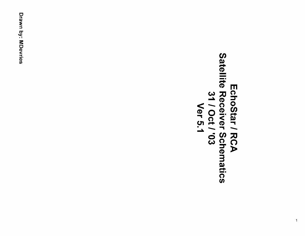
1
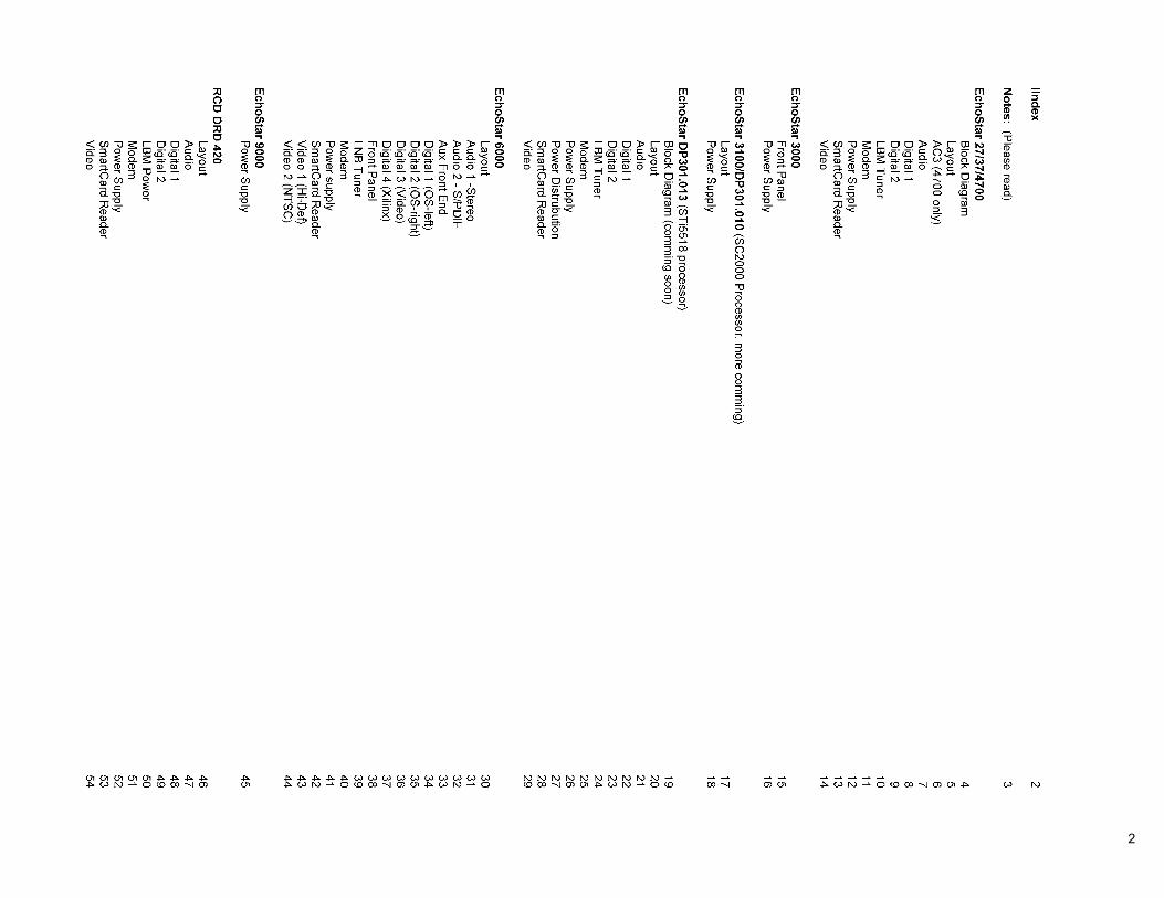
2
3
LBN Tuner(HM1811)
NVRAM(24L16)
CPUDemux
A/V Decoder(STi5500)
Audio Dac(PCM1720)
Right
Left
Sum Modulator
Svideo
27MhzClock
Buffer
SVHS Y
SVHS C
Comp Video
Buffer &Audio Trap
SDRAM
IR / UHF sensors
SmartCardReader
Front PanelButtons, Power LED
I2CI2C
IQ Demod(HM1211)
MPEG
I2C
13/18V Gen(LNBP20CR)
ACLK
I2S
Luminance
Chrominance
Composite Video
SMUART
General I/O
MPEG
IR Blast
SPDIF
Left AudioRight Audio
RF in
RF out
CompositeVideo out
13/18V
Data Stream
S-Video Out
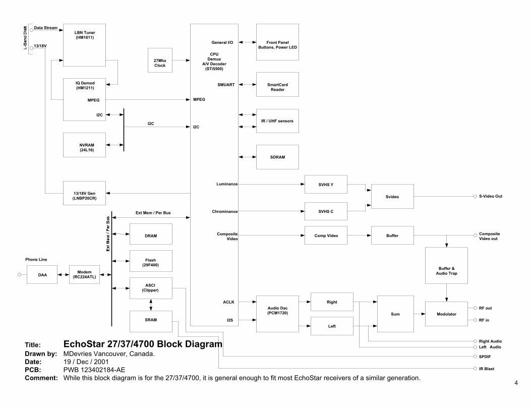
Title: EchoStar 27/37/4700 Block DiagramDrawn by: MDevries Vancouver, Canada.Date: 19 / Dec / 2001PCB: PWB 123402184-AEComment: While this block diagram is for the 27/37/4700, it is general enough to fit most EchoStar receivers of a similar generation.
Modem(RC224ATL)DAA
SRAM
DRAM
Flash(29F400)
ASCI(Clipper)
Ext Mem / Per Bus
Phone Line
4
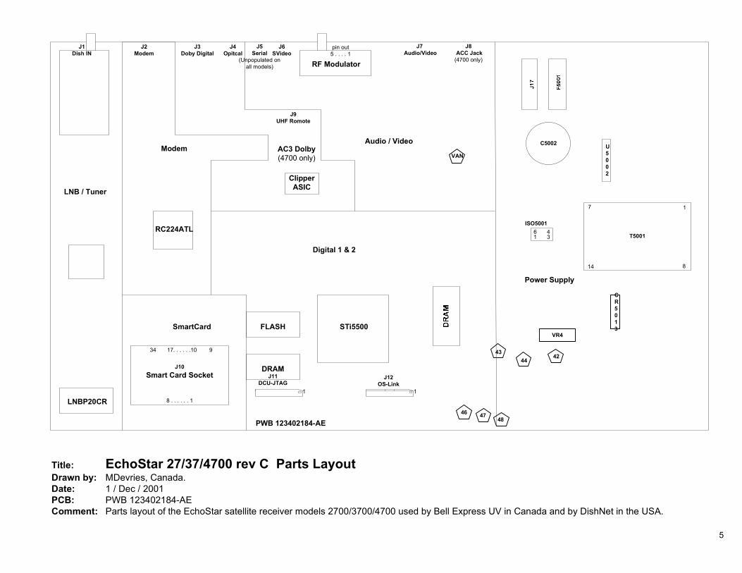
Title: EchoStar 27/37/4700 rev C Parts LayoutDrawn by: MDevries, Canada.Date: 1 / Dec / 2001PCB: PWB 123402184-AEComment: Parts layout of the EchoStar satellite receiver models 2700/3700/4700 used by Bell Express UV in Canada and by DishNet in the USA.
T5001
CR5013
C5002 U5002
VR4
4648
4244
VAN
ISO5001
47
17
814
1 346
43
Smart Card Socket
PWB 123402184-AE
Audio / Video
Digital 1 & 2
Power Supply
Modem
SmartCard
LNB / Tuner
STi5500
RC224ATL
LNBP20CR
FLASH
DRAM
RF Modulator
J1Dish IN
J2Modem
J7 Audio/Video
J6SVideo
J5Serial
(Unpopulated onall models)
J4Opitcal
J3Doby Digital
J8 ACC Jack(4700 only)
J10J11
DCU-JTAGJ12
OS-Link
pin out5 . . . . 1
8 . . . . . . 1
34 17. . . . . .10 9
11
J9UHF Romote
AC3 Dolby(4700 only)
ClipperASIC
5
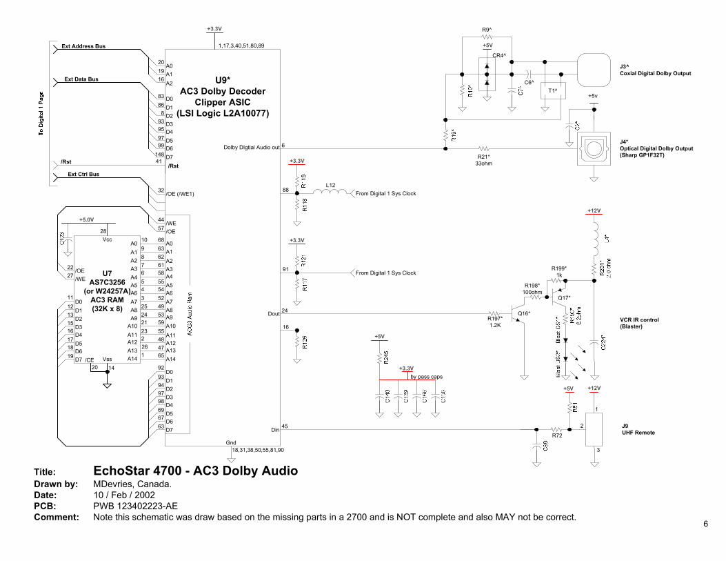
Title: EchoStar 4700 - AC3 Dolby AudioDrawn by: MDevries, Canada.Date: 10 / Feb / 2002PCB: PWB 123402223-AEComment: Note this schematic was draw based on the missing parts in a 2700 and is NOT complete and also MAY not be correct.
+5v
R21*33ohm
J3^Coxial Digital Dolby Output
J4*Optical Digital Dolby Output(Sharp GP1F32T)
CR4^
+5V
T1^
R9^
C6^
+12V
Q17*
R199*1k
R198*100ohm
Q16*R197*1.2K
VCR IR control(Blaster)
J9UHF Remote
1
2
3
+12V+5V
R72
10987654325242123
Vcc
+5.0V
U7AS7C3256
(or W24257A)AC3 RAM(32K x 8)
2261
28
Vss
D0D1D2D3D4D5D6D7
1112131516171819
/WE/OE22
27
6863626158555452
A0A1A2A3A4A5A6A7
49535955
A8
A10A11
A9
484765
A12
A14A13
A0A1A2A3A4A5A6A7A8A9
A10A11A12A13A14
D0D1D2D3D4D5D6D7
9293949798696763
/WE/OE
4457
14/CE
20 +3.3Vby pass caps
Dolby DIgtial Audio out
Dout
Din
6
24
45
201916
A0A1A2
Ext Address Bus
8386
893959799
148
D0D1D2D3D4D5D6D7
Ext Data Bus
/Rst 41/Rst
U9*AC3 Dolby Decoder
Clipper ASIC(LSI Logic L2A10077)
32 /OE (/WE1)
Ext Ctrl Bus
+3.3V
1,17,3,40,51,80,89
Gnd18,31,38,50,55,81,90
+3.3V
88L12
From Digital 1 Sys Clock
+3.3V
91 From Digital 1 Sys Clock
16+5V
6
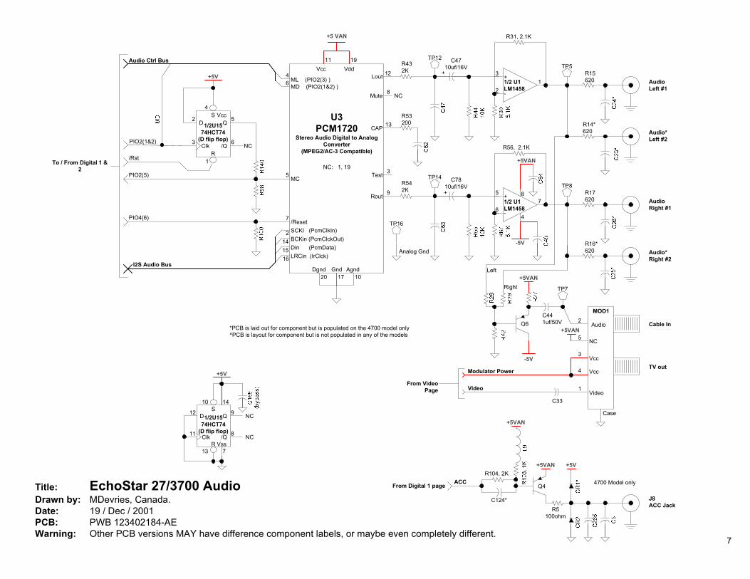
Title: EchoStar 27/3700 AudioDrawn by: MDevries, Canada.Date: 19 / Dec / 2001PCB: PWB 123402184-AEWarning: Other PCB versions MAY have difference component labels, or maybe even completely different.
+5V+5VAN
C124*
R104, 2K
Q4
+5VAN
R5100ohm
J8ACC Jack
From VideoPage
Vss7
14
D
/Q
QS
RClk
+5V
13
12
11
10
9
8
NC1/2U1574HCT74
(D flip flop)NC
Right
Cable In
TV out
Case
1
2
3
4
5
Video
Audio
Vcc
Vcc
NC
MOD1
-5V
C441uf/50V
TP7
Q6+5VAN
+5VAN
Video
Modulator Power
C33
Lout
Rout
Mute
CAP
19Vdd
U3PCM1720
Stereo Audio Digital to AnalogConverter
(MPEG2/AC-3 Compatible)
+5 VAN
11Vcc
MC5 Test
12
8 NC
13
3
9
ML (PIO2(3) )MD (PIO2(1&2) )
46
R31, 2.1K
R15620
R14*620
C4710uf/16V
AudioLeft #1
Audio*Left #2
TP5TP12
11/2 U1LM14582
3
-
+
R432K
R56, 2.1K
R17620
R16*620
C7810uf/16V
AudioRight #1
Audio*Right #2
TP8TP14
71/2 U1LM1458
5
6 -
+
4
R542K
R53200
-5V
+5VAN
+
+
Left
TP16
8
Analog Gnd
DVcc
/Q
QS
RClk
+5V
1
2
3
4
6
1/2U1574HCT74
(D flip flop)
5
NCPIO2(1&2)
PIO2(5)
To / From Digital 1 &2
/Rst
Audio Ctrl Bus
Din (PcmData)BCKin (PcmClckOut)
LRCin (IrClck)
SCKI (PcmClkIn)
1514
16
2
I2S Audio Bus
From Digital 1 page ACC
*PCB is laid out for component but is populated on the 4700 model only^PCB is layout for component but is not populated in any of the models
NC: 1, 19
1020Dgnd AgndGnd
17
/Reset7PIO4(6)
4700 Model only
7
U19STi5500
(ST20 CPU, Demux & A/V Decoder)
123
+5V
IRRemoteDector
Case
R195, 2.2K
IR1
A0A1A2A3A4A5A6A7A8A9A10A11
212223242728293031322019
Vdd
+5.0V
NC 33 & 37
23568911123940424345464849
D0D1D2D3D4D5D6D7D8D9D10D11D12D13D14D15
1517161814
/WE/RAS/CSA/CSLDQM
1,257,13,38,44VddQ
26,504,10,41,47VssVssD
D0D1D2D3D4D5D6D7D8D9D10D11D12D13D14D15
929394979899
100101106107108109112113114115
787980
6970717273748283
81
A0A1A2A3A4A5A6A7A8
A10A11
A9
CKECLKUDQM
343536
/SDCS0/SDCS1
/SDCASSDWE
8485888990
/SDRAS
MemClkIn (CKE)MemClkOut (Clk)
DqmU (Udqm)
1047691
105Dqml (Ldqm)
+3.3V
37363938
116
F_B_ClkF_DataF_Error / F_P_StartF_P_Clk / F_D_ValidLink_Ext_Clk
Transport Data StreamFrom LNB Tuner Page
3567
PIO2(0&1)
8PIO2(5)PIO2(4)PIO2(3)
Note:PIO2(2) does not exist.PIO2(1&2) are the same pin
PIO2(7)
To Video PagePowerMC To Audio Page
To Audio PageTo Audio PageMD
ML
To Video page
117118
OSD_Active27Mhz_Pix_Clock
/HsyncOdd_/Even
RG
515255565758
B
V_ref_Dac_RGBI_ref_Dac_RGB 59
NCNCNC
R158
NCNC
CrominanceLuminance&Sync 62
63646566
Composite VideoV_ref_Dac_YCCI_ref_Dac_YCC R155
NC
Note:Video section uses Vdda(53) & Vssa (54) for itspower
Brm0/OS-LinkSel 26
15151617
PIO0(0) / SC1DataOut
SmartCard Bus
20PIO0(4) / SC1ResetPIO0(3) / SC1Clock
PIO0(2) / No pin
PIO0(1) / SC1DataIn
Note:PIO0(2) does not exist.PIO0(1&2) are the same pin
PIO0(5) / SC1CmdVccPIO0(6) / ASC0 Dir
PIO0(7) / SC1Detect
2122
To/From SmartCard
9910
PIO1(0) / I2C MTSR
PIO1(2) / I2C ClkPIO1(1) / I2C MRST
PIO1(5) / ASC1TxD
Note:-PIO1(0&1) are the same pin
PIO1(4) / Capture 2PIO1(3) / Capture 1
PIO1(6) / ASC1RxDPIO1(7) / ASC3TxD
198
12
19911
13
+5V +5V
To 4700 Sys ClkTo AC3
To Audio
Vdd & Vdda'
1,18,34,49,53',67,75,86,95102,110,119,130,134,138,139,149,159,171,184,208
IC2 Buss
To Tuner LNB Tuner
Note: Brm0/OS-LinkSel (pin 26)should be held low during resetvia a resistor inorder to putSTi5500 into OS-Link Mode
PcmClkOut / ACStbPcmData / ACData
PcmClk_InIrClk/AC Clk
AC_RegAPtsStb
4344
4546
4748
I2S Audio BusTo Audio Page
AC3 Audio Bus To AC3 Page*(4700 only)
(PCMClkOut(BCKin), PCMData(Din), PCMClkIn(SCKI), IrClk(LRCin) )
(ACStb, ACData, ACClk, ACReg, APtsStb)
Note:Some pins of the Audio port have dual functionsdepending on the mode. In one case the pins functionas an I2S digital audio bus. In this case they use thePCM label. The other mode, used only by the 4700 andonly if selected, is the Doby AC3 mode. In this case thepins use the A or AC label.
+5V
R244(0Ohm)
* PCB is laid out for both two PowerGood ICs, U12 and U14. These twoICs have different pin outs and onlyone will be populated.
1
5
6
9
2/8 U4^SN75185
J5^SerialInterface
9
5
12
16
ACC
/Rst29
+3.3VdcVR3(TO-92)
Sti5500 Power
from +5V supply
53
2
L14
R109
TP31
+5V
7X1
4
U10^Sys ClockMK2773
(4700 only)
U11Sys ClockMK2727S
(2/3700 only)
GndGnd
Vcc Vcc
VinClk (27Mhz)
X21
Y213.5Mhz
832
1714
6
10
+5V
5
4, 6, 16
1
20
PIO4(3)
111213
7
AC3-29AC3-28AC3-27
19
18
98
AC3-xxAC3-xx
NC
16NC
Note: To program EEPROM, short OJ2 (on digital 2), check voltagelevels and hook up to SB78 & SB79. Then use any I2C progamingsoftware such as "PonyProg" @ www.Lancos.com to program or useone of the many Jtag programs available on the net.WARNING: There are several different PCB layouts for the 2/3/4700 andSB78/79 may be labled differently in some of the other layouts.
U4^6/8 SN75185
2
3
8
7
6
4
13
14
15
17
18
1920
NC
NC
NC
NC
NC
NC
-5V
11 10
+12V +5V
To Smart Card
+12VU4 bypass caps
+5V-5V
SB79SB78+5V
Vcc
Vss
A0A1A2
123
4
8
U21Config
EEPROM24LC16BWP
SCLSDA5
67
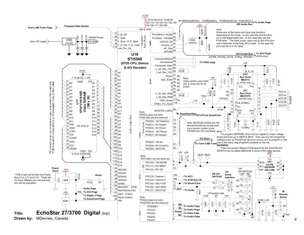
Title: EchoStar 27/3700 Digital (top)Drawn by: MDevries, Canada.
+5VPowerGood
/Rst+5V
U14
U12*To SmartCard Page
To AC3 PageAudio Page
To Digital 2 Page
R122 S1*
Reset
8
NC
NCNCNC
30
333231
SdavClk/P1394Clk
OSCSdac/P1394PClk
SdavData
TclkTdi
TdoTms/Trst
188186189187190
201202203204
PIO3(0) / OS_LinkDataIn
OS-Link Bus
205PIO3(4) / CPUErrorPIO3(3) / CPUAnalysePIO3(2) / CPUResetPIO3(1) / OS_LinkDataOut
CPUError
CPUAnalyseCPUReset
OS_LinkDataOut
Note: In order to accessthe OS_Link you musthold BRM / OS_Link_Sel(pin26 on the digital 1page) low via a resistorduring reset.
1211 109
87
13 14
+5V
3/6 U22^(assumes 74HC04/14)
(viewed from top)
J12OS_Link^
NC1 2
19 20
1/6 U22^56
R188^
1/6 U22^34
R176^
1/6 U22^21
R175^
OS_LinkDataIn
PIO3(5)PIO3(6)PIO3(7)
2062072
To LNB Tuner
Jtag Bus
J11DCU_JTag
(View from the bottom)
TclkTdi
Tdo
Tms
/Trst
Tclk
Tdi
Tdo
Tms
/Trst/Rst
/Rst
PIO3(7)PIO3(6
)
NC 3
4
5
6
7
1
2
1 2
19 20
BtSrc1 1
Seen through hole inbottom of Receiver
+3.3VR163Brm1/BootFromRom
27Brm228
NC
TP40 +3.3V
OJ2
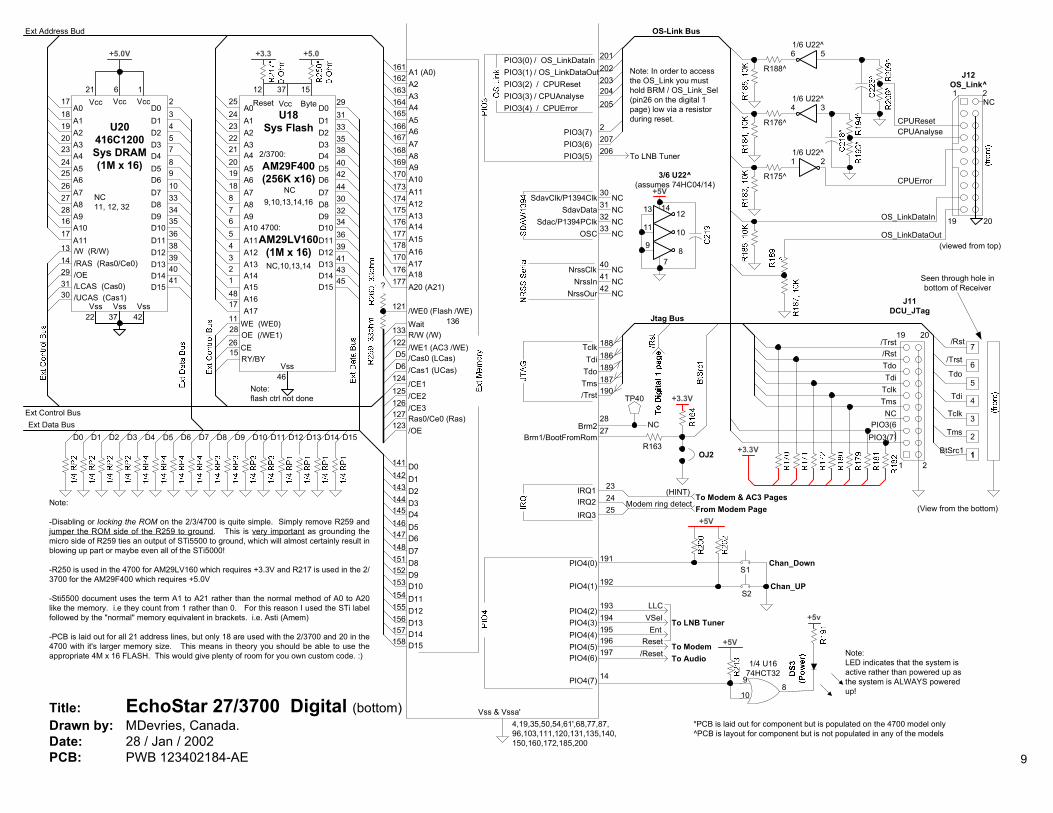
Title: EchoStar 27/3700 Digital (bottom)Drawn by: MDevries, Canada.Date: 28 / Jan / 2002PCB: PWB 123402184-AE
S2
S1Chan_Down
Chan_UP
+5V
Vcc ByteU18
Sys Flash
2/3700:AM29F400(256K x16)
NC9,10,13,14,16
4700:AM29LV160
(1M x 16)NC,10,13,14
29313335384042443032343639414345
D0D1D2D3D4D5D6D7D8D9D10D11D12D13D14D15
262811
15 CEOE (/WE1)WE (WE0)
RY/BY
A0A1A2A3A4A5A6A7A8A9A10A11A12A13A14A15A16
2524232221201918876543214817
A17
A0A1A2A3A4A5A6A7A8A9A10A11
171819202324252627281617
Vcc
+5.0V
NC11, 12, 32
U20416C1200Sys DRAM(1M x 16)
2345789103334353638394041
D0D1D2D3D4D5D6D7D8D9D10D11D12D13D14D15
1314293130
/W (R/W)/RAS (Ras0/Ce0)/OE/LCAS (Cas0)/UCAS (Cas1)
1621VccVcc
Vss423722VssVss
46Vss
A1 (A0)A2A3A4A5A6A7A8
A10A11
A9
A12A13
161162163164165166167168169170173174175
R/W (/W)Wait/WE0 (Flash /WE)
/WE1 (AC3 /WE)/Cas0 (LCas)/Cas1 (UCas)
/CE1/CE2/CE3Ras0/Ce0 (Ras)/OE
133136
121
122D5D6
124125126127123
Reset12 37 15
Ext Control BusExt Data Bus
Note:flash ctrl not done
141142143144145146147148151152153154155156157158
D0D1D2D3D4D5D6D7D8D9D10D11D12D13D14D15
Ext Address Bud
A15A16
A14
A17
176177178170
A20 (A21)A18176
177
Note:
-Disabling or locking the ROM on the 2/3/4700 is quite simple. Simply remove R259 andjumper the ROM side of the R259 to ground. This is very important as grounding themicro side of R259 ties an output of STi5500 to ground, which will almost certainly result inblowing up part or maybe even all of the STi5000!
-R250 is used in the 4700 for AM29LV160 which requires +3.3V and R217 is used in the 2/3700 for the AM29F400 which requires +5.0V
-Sti5500 document uses the term A1 to A21 rather than the normal method of A0 to A20like the memory. i.e they count from 1 rather than 0. For this reason I used the STi labelfollowed by the "normal" memory equivalent in brackets. i.e. Asti (Amem)
-PCB is laid out for all 21 address lines, but only 18 are used with the 2/3700 and 20 in the4700 with it's larger memory size. This means in theory you should be able to use theappropriate 4M x 16 FLASH. This would give plenty of room for you own custom code. :)
?
+3.3 +5.0
D15D14D13D12D11D10D6 D8D7 D9D5D4D2 D3D1D0
4,19,35,50,54,61',68,77,87,96,103,111,120,131,135,140,150,160,172,185,200
Vss & Vssa'
10
98
+5v
1/4 U1674HCT32
+5V
191
192
193194
PIO4(0)
195PIO4(4)PIO4(3)PIO4(2)
PIO4(1)
PIO4(5)196
PIO4(6)197
PIO4(7) 14
Note:LED indicates that the system isactive rather than powered up asthe system is ALWAYS poweredup!
To LNB Tuner
To ModemReset
To Audio/Reset
23IRQ1IRQ2IRQ3
2425
Modem ring detect From Modem Page
(HINT) To Modem & AC3 Pages
NC
NCNC
40
4241
NrssClk
NrssOurNrssIn
LLCVSelEnt
*PCB is laid out for component but is populated on the 4700 model only^PCB is layout for component but is not populated in any of the models
9
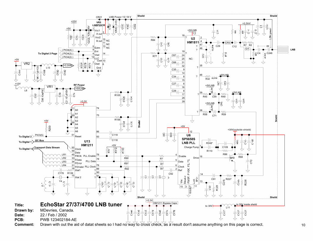
Title: EchoStar 27/37/4700 LNB tunerDrawn by: MDevries, Canada.Date: 22 / Feb / 2002PCB: PWB 123402184-AEComment: Drawn with out the aid of datat sheets so I had no way to cross check, as a result don't assume anything on this page is correct.
L11to 30V inside sheildto 30V
+3.3VHM1211 Bypass Caps
+3.3V
LR1LR2LR3LR4
To Digital 1 Transport Data Stream
FBClkFDataFErrorFDValid
45333431
C118
C11986
93
U13HM1211
919089
???
+5V
78
78
78
PLL Enable
PLL Data
PLL Clock
R139
Y4
C178
+ + +
I2C BusTo Digital 1
4950
DataClock
51 ResetPIO3(5)To Digital 2
+5V
A0A1A2A3A4A5A6
71
69
56
15
U6SP5658SLNB PLL
4
5
6
Enable
Data
ClockRef
C92
R?
R?
R? 2
3
R90
R91
R92
13C91 R227
14
Drive
Charge Pump C109
R86
+30V(outside shield)
R68
R248*
R110
1
16
11
+5V
12
VR5LNBP20CR
+5V
Vcc2A out
B out
Vcc1
Cext
NCNCNC
Gnd
LLC
CR21
Vsel
Extm
Osel
Ent
8
7
1
23
4
59
10
11
12
13
15
14
6
To Digital 2 Page( PIO4(4) )( PIO4(3) )( PIO4(2) )
+22V
LNB Power 13/ 18 V
U2HM1811
NC:
C28 817
C27 616
C35 914
C34 815
C68 3132
C67 2425
2628
C54
C71
R45
R58 R59
R49
+5VLNB
+5VLNB
+5VLNB39
38
?
?
4647?
?
? +5VLNBR32
48uLine
C12C29 R7 R2Q1
C4 C246
Rf
24 CR3
+5VLNB1,2
?R84
18
19?
R77
35?
LNB
Sheild
R106
R105
+3.3VRfVR2+5V
L13
+5VLNBVR1+12V
L8
RF Power
Sheild
Sheild Sheild
Q13
+3.3Vrf
15
16Xtal1
Xtal 2
75
74
10
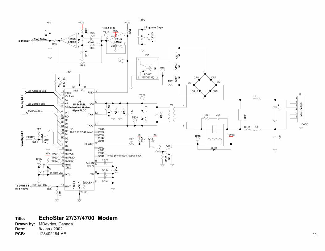
Title: EchoStar 27/37/4700 ModemDrawn by: MDevries, Canada.Date: 9/ Jan / 2002PCB: 123402184-AE
+12V
U5 bypass Caps
15
+5VdcTP18
Ext Contorl Bus
OHrelay
RING
Ext Data Bus
U8RC244ATL
Embedded Modem68pin PLCC
WTRD62
636465676812
45
14
40
3
108
11
NC18,20,30,37,41,44,46,
IDLEN1
A0A1A2
D0D1D2D3D4D5D6D7
CR14
C57R33
PC817(ECG3098)
ISO1
4
3 2
1
R27
L4
L2RT11
4321
56
CASE
J2TP29
T1
1
2
CR9
CR8
CR10
CR7
+
-
ACAC
TP17
RXA
TXA1
TXA2
33
32
31
Q18R791K
+5V
VccNMIHDIS
+5+5R871K
Q12
TP28
C149
C150
VC
C130
21
17
IDLEN0
66
12
29/4928/5227/5026/4725/45
24/5248/2322/4355/42
Reset
C155
C171 16.0003MhzY3
These pins are just looped backTP35
/Test57
+5V
RFILOAGCIN
36
3435
TP23TP27
TP24
39 60
Ext Address Bus
NVRDIONVRSK
NVRCS1913
7
XTL0
/XTL1
59
58
1
6
5 4
3
2
8
Vss
Vcc
+
-
+
-
+12V
+12V+5V
7
TP15
R74
R75
1/2 U5LM358
1/2 U5LM358
R89
R88
+12V
C101
1bit A to D
Ring DetectTo Digital 1
R3616 HINTTo Ditial 1 &
AC3 PagesIRQ1 (pin 23)
Q19R254
+5V
PIO4(5)
11
CR5001 CR5002
CR5003 CR5004
F50012A Slow
C5024C5001
L2
N1
C5032
C5021 R50294M7
L5006J71115Vac
R50344M7
CR5008
1
2
4
3
5
7
6
ISO5001
R503120 ohm CR5007
R50053K9
Vcc
OSC VIPer 50Control
5
2
1
3
4
+30 VdcL5005
+22 VdcL5004
+5VdcL5001
+5Vdc
L5002
- 5Vdc
+12VdcL5003
13
9
14
11
10 & 12
CR012
CR1013
CD5011
CR5014
CR5016~150Vdc
~12Vdc
C5024
R5004
2.5Vdc
1 2 3
4 5 6
CYN-17F(ECG3041)
T5001
+3.3Vdc
R5009
VR4
R5013
10 & 12
1
6
5
2
R A
TL341
C
T5001
1
23456
7
89
10
111213
14
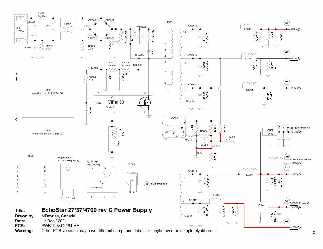
Title: EchoStar 27/37/4700 rev C Power SupplyDrawn by: MDevries, Canada.Date: 1 / Dec / 2001PCB: PWB 123402184-AEWarning: Other PCB versions may have different component labels or maybe even be completely different.
43
48
46
VAN
47
42
44
R501015 ohm
1
+3.3VdcVR3(TO-92)
Audio/Video Power
Sti5500 Power #1
Sti5500 Power #2
TL341
PQ3RD083 ?(3.3Vdc Regulator)
+5 +3.3 +5
12 PCB Test point
timeWaveform pin 5 of VIPer 50
timeWaveform pin 3 of VIPer 50
12
J10SmartCard SocketCR25*
+5V
1
2
3
4
5
6
7
8
9
10
11
12
13
14
37
34
15
16 NC
NC
NC
NC
CR22*
+5V
CR23*
+5V
CR24*
+5V
+5V
SC CLK
SC Detect
R142
R205
R204
R203
SC Vcc
TP39+5V
R150
R206
1312
1/6U2474HCT14
1 2
5 6
3 4
7
+5V
1/4U1674HCT32
2
13
1/4U1674HCT32
5
46
98
1/6U2474HCT14
1110
1/6U2474HCT14
C189
+5V
R148SC1 Clk R262
R262
SC1 Reset
SmartCard
SmartCard Detect SwtichOpen when card is inserted(part of socket)
GND
GndVcc
I/OResetClk
+5V
SC1 Detect
SmartCard buss
SC TRXD (PIO0-0/1)
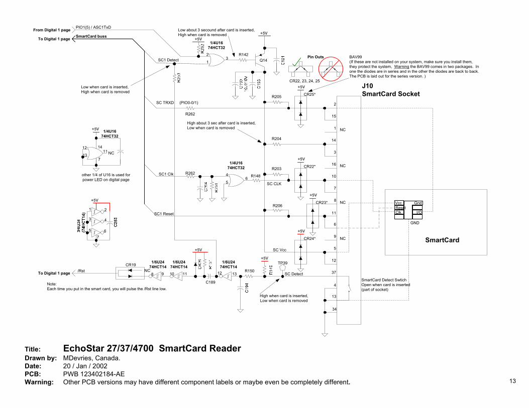
Title: EchoStar 27/37/4700 SmartCard ReaderDrawn by: MDevries, Canada.Date: 20 / Jan / 2002PCB: PWB 123402184-AEWarning: Other PCB versions may have different component labels or maybe even be completely different.
other 1/4 of U16 is used forpower LED on digital page
To Digital 1 page
NCCR19
/Rst
Note:Each time you put in the smart card, you will pulse the /Rst line low.
To Digital 1 page
Q14
High when card is inserted,Low when card is removed
Low when card is inserted,High when card is removed
13
1211 NC
+5V 1/4U1674HCT32
14
7
High about 3 sec after card is inserted,Low when card is removed
Low about 3 secound after card is inserted,High when card is removed
From Digital 1 page PIO1(5) / ASC1TxD
BAV99(If these are not installed on your system, make sure you install them,they protect the system, Warning the BAV99 comes in two packages. Inone the diodes are in series and in the other the diodes are back to back.The PCB is laid out for the series version. )
Pin Outs
CR22, 23, 24, 25
13
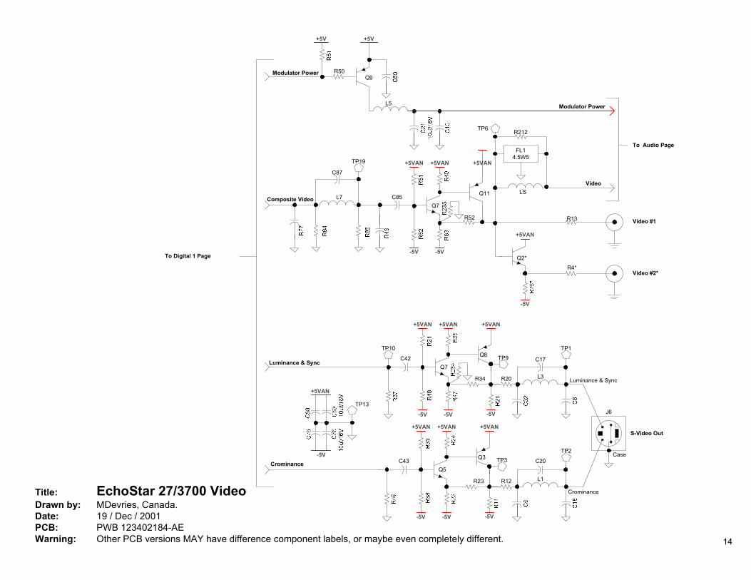
Title: EchoStar 27/3700 VideoDrawn by: MDevries, Canada.Date: 19 / Dec / 2001PCB: PWB 123402184-AEWarning: Other PCB versions MAY have difference component labels, or maybe even completely different.
TP1
R20 L3
C17
Luminance & Sync
Crominance
TP9
TP3
R12 L1
C20
TP2
Q8
R34
C42Q7
+5VAN+5VAN+5VAN
-5V -5V -5V
Q3
R23
C43Q5
+5VAN+5VAN+5VAN
-5V -5V -5V
J6
Case
S-Video Out
TP10
-5V
+5VAN
TP13
Luminance & Sync
Crominance
Video #1R13
R4*Video #2*
Q11
R52
C85Q7
+5VAN+5VAN+5VAN
-5V -5V
C87
L7
TP19
-5V
+5VAN
Q2*
Composite Video
TP6
FL14.5W5
LS
R212
Video
+5V
L5
Q9
+5V
R50Modulator Power
To Audio Page
Modulator Power
To Digital 1 Page
14
2
10
CR4S5Left
CR8S2Up
CR1S8Down
CR5S6Right
CR6S7Select
CR7S3Power
CR3S1Info
CR2S4Menu7
8
9
6
5
4
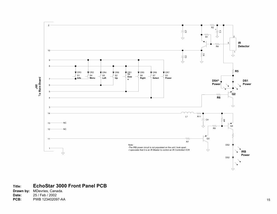
Title: EchoStar 3000 Front Panel PCBDrawn by: MDevries, Canada.Date: 25 / Feb / 2002PCB: PWB 123402097-AA
R2
R4
R1
+
IRDetector
2
1
3
DS1Power
R5
Q2R6
DS4^Power
IRBPower
DS2
DS2
Q3R7
R9Q4
C4L1 R11
12 NC
13 NC
1
11
14
3
Note:-The IRB power circuit is not populated on the unit I took apart.-I speculate that it is an IR Blaster to control an IR Controlled VCR
15
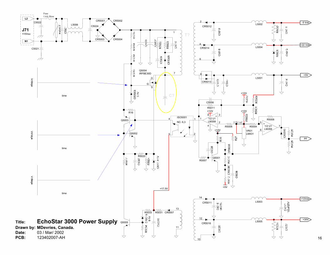
Title: EchoStar 3000 Power SupplyDrawn by: MDevries, Canada.Date: 03 / Mar/ 2002PCB: 123402007-AH
+22 VdcL5004
4
6
-5 VdcL50022
CR5014
CR5012
+5VL5001
8
CR5013
CR5001 CR5002
CR5003 CR5004
Fuse1.6A Slow
C5024
L2
N1
C5022
C5021
L5006
J71115Vac 1
7
D
GS
14 +12VdcL5003CR5011
+30VL5005
12
10
CR5016
ISO500114
5 2
3
21
+
-
1/2 U1LM358
8
46
57
+
-
1/2 U1LM358
R5008
PF
+12V
2.5V refR5008
+12VR5011
C5006
R5004
R5007
+12V VR01LM431
+12V
Q5001
+5V
NC: 6,3
R5020
13
11
CR5007R5031R5033
Q5005
Q5004IRFBE30D
R16
Q5003
Q5002
+17.5V
T?
C?time
time
time
16
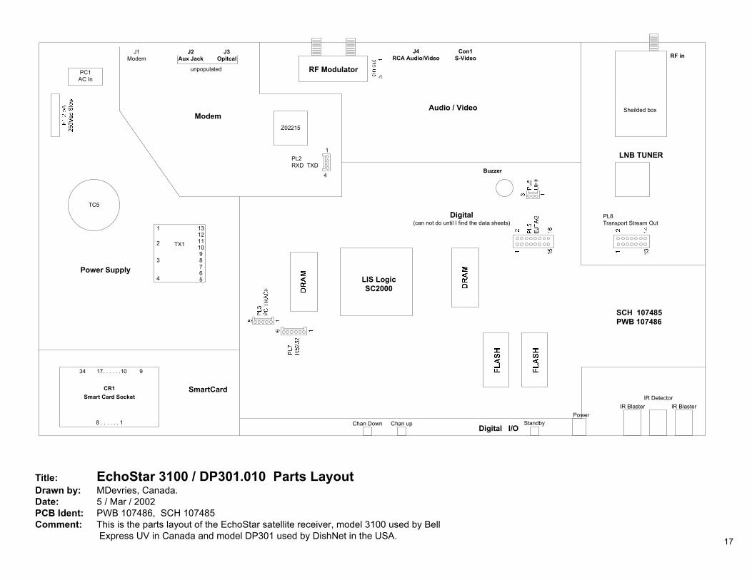
Title: EchoStar 3100 / DP301.010 Parts LayoutDrawn by: MDevries, Canada.Date: 5 / Mar / 2002PCB Ident: PWB 107486, SCH 107485Comment: This is the parts layout of the EchoStar satellite receiver, model 3100 used by Bell
Express UV in Canada and model DP301 used by DishNet in the USA.
Smart Card Socket
SCH 107485PWB 107486
Audio / Video
Digital(can not do until I find the data sheets)
Modem
SmartCard
Power SupplyLIS LogicSC2000
RF Modulator
J1Modem
J4RCA Audio/Video
J3Opitcal
J2Aux Jack
Con1S-Video
CR1
8 . . . . . . 1
34 17. . . . . .10 9
RF in
Digital I/OChan Down Chan up Standby
Power
IR DetectorIR Blaster IR Blaster
LNB TUNER
PC1AC In
TC5
unpopulated
Sheilded box
Buzzer
TX1
1
4
2
3
56789
10111213
PL2RXD TXD
1
4
PL8Transport Stream Out
Z02215
17
1+30 Vdc
13
D23~150V TX1
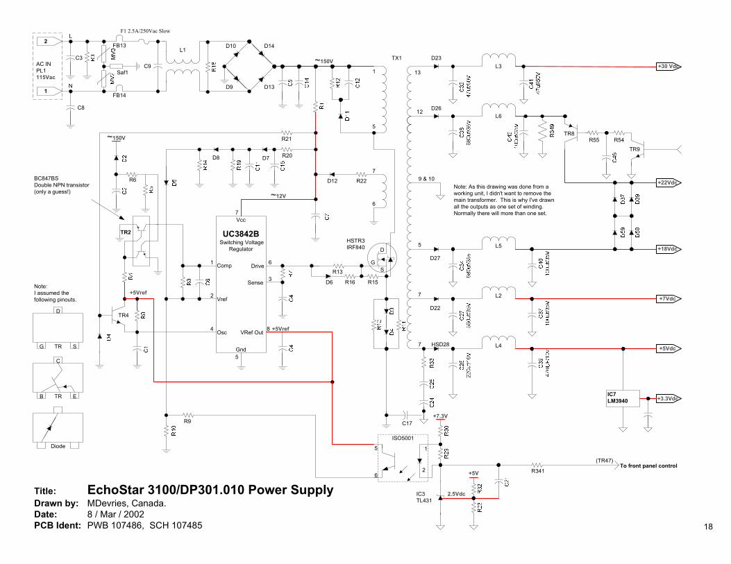
Title: EchoStar 3100/DP301.010 Power SupplyDrawn by: MDevries, Canada.Date: 8 / Mar / 2002PCB Ident: PWB 107486, SCH 107485
D10 D14
D9 D13
L1
F1 2.5A/250Vac Slow
C9
2
1
C3
C8
AC INPL1115Vac
Saf1
FB13
FB14
D
GS
5
7
6
D12 R22
1
2
Comp
Vref
UC3842B Switching Voltage
Regulator
5
7
6
4
Gnd
Osc
Drive
Vcc
3Sense
8VRef Out +5Vref
~12V
R6
R9
TR4
~150V
TR2
+5Vref
R20
R21
D8 D7
TRB
C
E
Diode
TRG
D
S
Note:I assumed thefollowing pinouts.
L3
9 & 10
L5
D27+18Vdc
L2
D22+7Vdc
12 D26
+22Vdc
L6
HSTR3IRF840
R15D6
R13
R16
Note: As this drawing was done from aworking unit, I didn't want to remove themain transformer. This is why I've drawnall the outputs as one set of winding.Normally there will more than one set.
BC847BSDouble NPN transistor(only a guess!)
5
7
L4HSD28+5Vdc
7
C17
2.5Vdc
ISO5001
1
6
5
2 +5V
+7.3V
To front panel controlR341
R55 R54TR9
L
N
IC3TL431
TR8
+3.3VdcIC7LM3940
(TR47)
18
3100/DP301.010 (STi) block Diagram - Being worked on- Comming soon
19
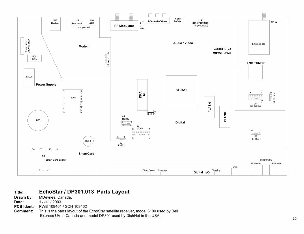
Title: EchoStar / DP301.013 Parts LayoutDrawn by: MDevries, Canada.Date: 1 / Jul / 2003PCB Ident: PWB 109461 / SCH 109462Comment: This is the parts layout of the EchoStar satellite receiver, model 3100 used by Bell
Express UV in Canada and model DP301 used by DishNet in the USA.
Smart Card Socket
Audio / Video
Digital
Modem
SmartCard
Power Supply
J13Modem
RCA Audio/VideoJ16AC3
J12Aux Jack
Con1S-Video
CR1
8 . . . . . . 1
34 17. . . . . .10 9
RF in
Digital I/OChan Down Chan up Standby
Power
IR DetectorIR Blaster IR Blaster
LNB TUNER
J5001AC In
TC5
unpopulated
Shielded box
T5001
1
5
2
3
14131211109876
4
L5005
J6FE MPEG
STi5518
J9FE TEST
15
RF Modulator
J14UHF UPGRADE
(unpopulated)
J2RS232
15
J3JTAG 1
2
19
20
1569
J4RS232
Buz 1
J7 UHF1 5
20
Lout
Mute
CAP
19Vdd
U18PCM1720
Stereo Audio Digital to AnalogConverter
(MPEG2/AC-3 Compatible)
+5 VAN
11Vcc
12
8 NC
13
R274
R275*
AudioLeft #1
Audio*Left #2
TP52
R199
To / From Digital 1 &2
NC: 1, 19
1020Dgnd AgndGnd
17
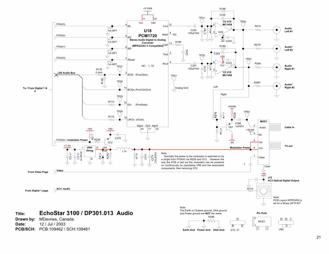
Title: EchoStar 3100 / DP301.013 AudioDrawn by: MDevries, Canada.Date: 12 / Jul / 2003PCB/SCH: PCB:109462 / SCH:109461 DAA GndPower Gnd
R288
Note:The Earth or Chassis ground, DAA groundand Power ground are NOT the same.
Earth Gnd
13
2 -
+4
1/2 U19MC1458
-5V C245
C232
C230100uf/16V Gnd
TP31
R188
/Reset7
MC5
ML
MD6
From Video Page Video
Pin Outs
MOD11
5C
EBQ12, 21
G IO
GVR9
PIO4(3)
1/4 RP7
4
1/4 RP7
1/4 RP7
1/4 RP7
PIO4(2)
PIO4(1)
PIO4(0)
Din (PcmData)
BCKin (PcmClckOut)
LRCin (IrClck)
SCKI (PcmClkIn)
15
14
16
2I2S Audio Bus
R172
TP26
TP29
TP28
TP27
R172
R1760 ohm
J12AC3 Optical Digital Output
R174
+5V
AC3- Audio
Note:PCB Layout APPEARS tobe for a Sharp GP1F32T
+5V
L14
C275Q12
+5V
R228PIO4(4) / modulator Power
VR9*5Vreg
I O
G
+7.5V+5Vmod
Rout
Test 3
9 R268
R269*
AudioRight #1
Audio*Right #2
TP51
TP41
Analog Gnd
R189
75
6 -
+
Vcc
1/2 U19MC1458
C324
C231100uf/16V
TP32 +5V
8 C233
+5VAN
Left
Cable In
TV out
Case
1
2
3
4
5
Video
Audio
Vcc
Vcc
NC
MOD1
-5V
C2961uf/50V
TP53
Q21+5VAN
?
Modulator Power
Right
From Digital 1 page
Note: Normally the power to the modulator is switched on bya single from PIO4(4) via R228 and Q12. However theway the PCB is laid out the modulator can be poweredon continuously by populating VR9 and the associatedcomponents, then removing Q12.
21
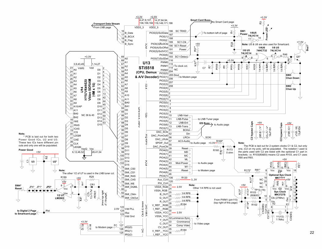
U13STi5518
(CPU, Demux & A/V Decoder)
BA1
A0A1A2A3A4A5A6A7A8A9A10/APA11
232425262930313233342233
NC 36 & 40
24578911134244454746505153
D0D1D2D3D4D5D6D7D8D9D10D11D12D13D14D15
/WE/RAS/CAS/CSLDQM
696867
5859606162637071
66
A0A1A2A3A4A5A6A7A8
A10A11
A9
CKECLKUDQM
1618171939373839
BA0BA2
D0D1D2D3D4D5D6D7D8D9D10D11D12D13D14D15
84858687888990919293979899
100101102
SMI_DQML
BA0
Vdd
+3.3V
1,14,273,9,43,49VddQ
28,41,546,12,46,52VssVssQ
7273
SMI_CS0SMI_CS1
SMI_CASSMI_WE
7475767778
SMI_RAS
U
SMI_ClkOut
79808295
SMI_ClkIn
Transport Data StreamFrom LNB page
16
191817
B_DataB_BCLKB_FlagB_Sync
4,47,8,107,136,159,184
+3.3V
VDD3_3
14,37,64,94,119,149,171,198
+2.5V
VDD2_5
41 MCPIO4(2)
40 MDPIO4(1)
39 ResetPIO4(0)
to Audio page42
Mod-PowerPIO4(3)
43M1
PIO4(4)PIO4(5)
44
PIO4(7)4645 /Reset
PIO4(6)to Modem page
ML
From PWM1 (pin115)(top right of this page)
Smart Card Buss
PIO0(2)
186PIO0(0)/Sc0Data
SC TRXD187
PIO0(1)
5
46
1/4U674HCT32
+7.5V
5 6
1/6 U574LVC14
A R46Q5*9 8
1/6 U574LVC14
A
188
115
192PIO0(6)
PWM1
189190
PIO0(3)/Sc0ClkPIO0(4)/ScORst
SC1-ClkSC1-Reset
191PIO0(5)/Sc0VCC
193PIO0(7)/Sc0Det
SC1-Detect
Power
116PWM0
114PWM2 NC
To clock cct.
+5V
to Smart Card page
11 10
+3.3V
1/6U574LVC14
To bottom left of page
Note: U5 & U6 are also used for Smartcard.
SW1Power
+3.3V
204
207PIO2(3)
PIO2(0)to Modem page
205 DoutPIO2(1)
206PIO2(2)
208PIO2(4)
1PIO2(5)
2PIO2(6)
3PIO2(7)
13 LNB-TransPIO3(7)
12 LNB-EntPIO3(6)
11 LNB-PulsePIO3(5)
10 LNB-VselPIO3(4)
to LNB Tuner page
9PIO3(3)
8PIO3(2)
7PIO3(1)
6PIO3(0)
+3.3V
SW3Chan Down
SW2Chan Up
C7
127FCIRQ(0)to Modem page
126IRQ(1)
125IRQ(2)
+3.3V34
3233
CV_OUT
Y_OUTC_OUT
Comp Video
Luminance-SyncCrominance
31
R1843635
V_REF__YCCI_REF__YCC
VSSA_RGB2.5V
23VDDA_RGB
24
R1842829
V_REF__RGBI_REF__RGB
26G_OUT
25B_OUT
27R_OUT
1/4 RP61/4 RP61/4 RP6
2.5V30
VDDA_YCCVSSA_YCC
to Video page
Note: The other 1/2 of U7 is used in the LNB tuner cct.
Note; * PCB is laid out for both twoPower Good ICs , U2 and U3.These two ICs have different pinouts and only one will be populated.
R189
13
2-
+Vcc
Vss1/2 U7
LM2903
+5V8
+5V
JP2*CR1
R29
SW4*Reset JP4* JP1*
+5VPower Good
U3 U2*
/Rstto Digital 2 Pageto Smartcard page
Vdd PLL2.5V122
123Vdd Gnd/Rst
124
120PIX_CLK
106Aux_CLK 3..3V
Note: Other 1/4 RP6 is not used
R120
53 7
X1
4
C2Sys ClockMK3727S
VinClk (27Mhz)
X218
C1*Optional Sys Clock
MK????
32
Y1(Y2)?.?Mhz
16
R81*
20
141719
111213
7
10
TP13 (16)
5
+5V
Vcc Vcc6
+5V
Vcc4 15
R103(80&93)
+5V
R102
1
9NC
18
NCNC
8R175*
Vcc Vcc2 6
+5V +5V
Note: The PCB is laid out for 2 system clocks C1 & C2, but onlyone, (C2 on my pcb), will be populated. The notation I used isthe parts used with C2 are listed with the opitional C1 part inbrackets. i.e. R103(80&93) means C2 uses R103, and C1 usesR80 and R93.
515256
DAC_SClkDAC_PcmOut0
DAC_LRclk
BCKinDin
LRCin
I2S Buss to Audio page
55DAC_PcmClk
57 AC3-AudioSPDIF_Out
SCKI
R1730 ohm
R160
+3.3Vto Audio pageR169*
22
4
53
12/4 U8MAX232
8
9NC
+3.3V
2 ~8V
710NC
11
~-8V
8
2/4 U8MAX232
121
3456789 P
+3.3V
G
TmsBtSrc1
TclkTdi
Tdo/Trst/Rst
TxRx
Note: To program EEPROM, putand keep the STi5518 into reset,hook up J5, then use any I2Cprogramming software such as"PonyProg" @ www.Lancos.comto program or alternately useone of the many Jtag programssuch as IRDr available on thenet.
1
5
6
9
J4RS232(RS232 Serial)
13
14
12
11
+5V
To Digital 1 page
R62/Reset
TclkTdiTdo
Tms
/Trst
112113
109111
110
Trigger_inTrigger_out
203204
+3.3V
NC
1
4
TclkTdi
Tdo
/Trst/Rst
TP10 TP9TP11 TP8 TP7
J3JTag
TmsNC
1 2
19 20
Trigger_inTrigger_out
+3.3V
+5V
+3.3V
197200
PIO1(3)/Uart2_TxdPIO1(4)/Uart2_Rxd
201PIO1(5)
196PIO1(2)
+3.3V
Note: -Disabling or locking the ROM on the 3100/DP301 is quite simple. Simply removeR110 and jumper the ROM side of the R110 to ground. This is very important asgrounding the micro side of R110 ties an output of STi5518 to ground, which will almostcertainly result in blowing up part or maybe even all of the STi5518! -STi documentation typically uses the term A1 to A21 rather than the normalmethod of A0 to A20 like the memory. i.e they count from 1 rather than 0. For thisreason I used the STi label followed by the "normal" memory equivalent in brackets.i.e. Asti (Amem).
Address Buss
Data Bus
Vcc Byte
U12Sys Flash
AM29LV160D(1M x 16)NC,10,13,14
CE46
Vss
Reset12 37 15
+5.0
26
A0A1A2A3A4A5A6A7A8A9A10A11A12A13A14A15A16
2524232221201918
87654321
4817
A17A18
169
A19
29313335384042443032343639414345
D0D1D2D3D4D5D6D7D8D9
D10D11D12D13D14D15
11
RY/BY
2815
OE (/WE1)WE (WE0)
Gnd
Y0Y1Y2
567
1/2 U974LVC139(2->4 mux)
Y3
42A
23
2B2G
1
7
NCNCNCNC
+3.3V
Vcc16
141142143144145146147148151152153154155156157158
D0D1D2D3D4D5D6D7D8D9D10D11D12D13D14D15
Control Buss
A11(A10)A12A13
174175
A15A16
A14
A17
176177178
A19A18
179180181
A1 (A0)A2A3A4A5A6A7A8
A10A9
161162163164165166167168169170173
A20A21(A20)
182183
Y0Y1Y2
111009
1/2 U974LVC139
(2 to 4 mux)
Y3
122A
14
132B
2G15
NCNC
R90*
A20(A21)
R92,0 ohm
A19(A18)R85,0 ohm
CPU_CAS(0)
R107,33 ohm
R108,0 ohm
CPU_CE(2)
A18(A17)
Control Bus
CPU_PROCLK
CPU_BE(1)
CPU_OE
CPU_Wait
R11633ohm
R131*33ohm
R11033ohm
CPU_BE(0)
CPU_CE(3)
CPU_CE(1)CPU_CE(0)
CPU_CE(2)
118
139
128
132133134135
140
138
129
117
130131
CPU_RW
CPU_RAS1CPU_CAS0CPU_CAS1
Vcc Byte
U10Sys Flash
AM29LV160D(1M x 16)NC,10,13,14
CE46
Vss
Reset12 37 15
+5.0
26
A0A1A2A3A4A5A6A7A8A9A10A11A12A13A14A15A16
2524232221201918
87654321
4817
A17A18
169
A19
29313335384042443032343639414345
D0D1D2D3D4D5D6D7D8D9
D10D11D12D13D14D15
11
RY/BY
2815
OE (/WE1)WE (WE0)
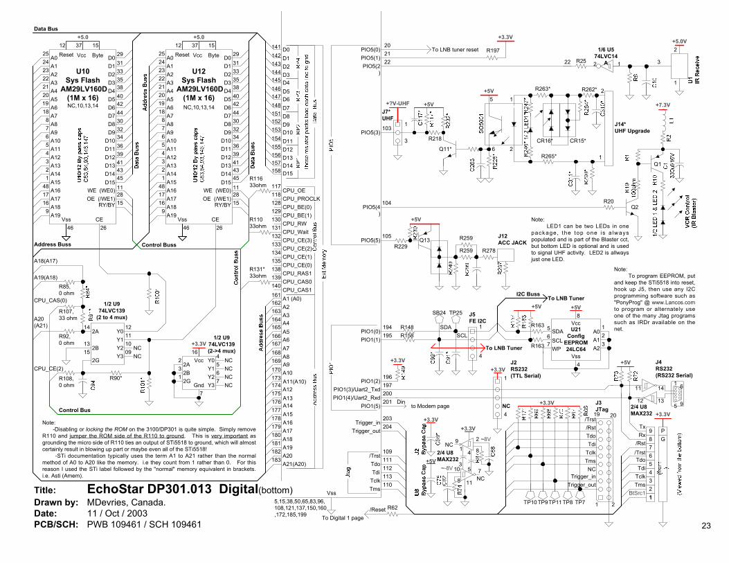
Title: EchoStar DP301.013 Digital(bottom)Drawn by: MDevries, Canada.Date: 11 / Oct / 2003PCB/SCH: PWB 109461 / SCH 109461
5,15,38,50,65,83,96,108,121,137,150,160,172,185,199
Vss
Dinto Modem page
J2RS232(TTL Serial)
SCLSDA
+5V
Vcc
Vss
A0A1A2
123
4
8
U21Config
EEPROM24LC64WP
SCLSDA5
67
+5V
R163
R163
TP25SB24 J5FE I2C
1
4To LNB Tuner
To LNB TunerI2C Buss
195PIO1(1)
194PIO1(0)
R148R158
Note: LED1 can be two LEDs in onepack age, the top one i s a lwayspopulated and is part of the Blaster cct,but bottom LED is optional and is usedto signal UHF activity. LED2 is allwaysjust one LED.
+?V-UHFJ7*UHF
1
3
103PIO5(3)
Q11*
+5V
R218
1
6
5
2
+5V R263*
CR16*
R265*
J14*UHF Upgrade
R262* 2
CR15*
1
104PIO5(4
)Q2
R20
+7.3V
Q1
PIO5(0) To LNB tuner reset20
PIO5(1)21
+3.3V
R197+5.0V
1
2
PIO5(2)
312
1/6 U574LVC14
AR252222
R278R259
R259Q13
+5V
R229
105PIO5(5)
J12ACC JACK
23
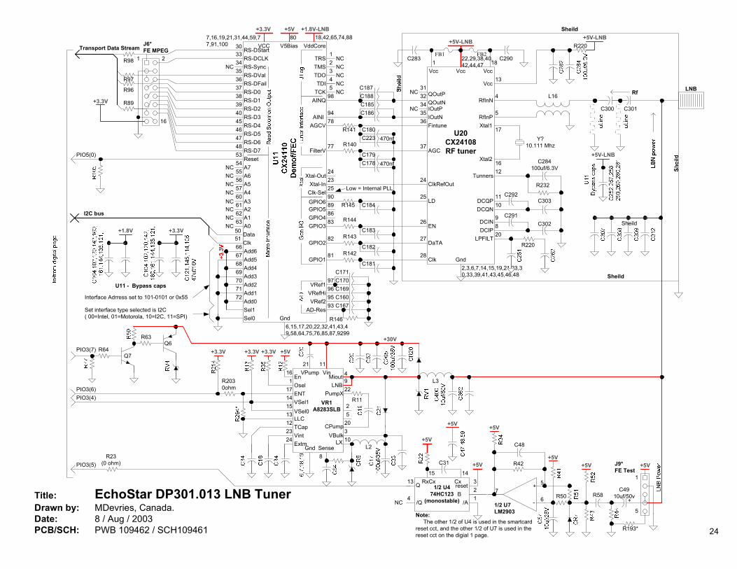
Title: EchoStar DP301.013 LNB TunerDrawn by: MDevries, Canada.Date: 8 / Aug / 2003PCB/SCH: PWB 109462 / SCH109461
NC
1
5
+5V
R193*
Sheild
Sheild
J6*FE MPEG
R98
R97
R96
R89
Transport Data Stream
1
16
2
3033
+3.3V
RS-DStartRS-DCLK
35
37
48
46
40
38
47
45
39
RS-DVal
RS-D0
RS-D7RS-D6RS-D5RS-D4RS-D3RS-D2RS-D1
36RS-DFail
34RS-SyncNC
U20CX24108RF tuner
2,3,6,7,14,15,19,21,23,30,33,39,41,43,45,46,48
+5V-LNB
20
R220
22,29,38,40,42,44,47
FB2FB1181
C283 C290
+5V-LNBR220
+5V-LNB
Y?10.111 Mhz
16
17
1110
C292C303
98
C291C302
C284100uf/6.3V12
R232
C300
Rf
C301
L164
5
LNB13
Vcc Vcc
Vcc
RfInN
RfInPXtal1
Xtal2
Tunners
DCQPDCQN
DCINDCIP
LPFILT
Gnd
VddCore12345
TRSTMSTDOTDI
TCK
NCNCNCNCNC
I2C bus
5051
DataClk
C187C18898C185C18694 35
AINQ
AINI
R141 C18078 36
C223 470nfR140
C17977 37
C178 470nf
AGC
FintuneAGCV
FilterV
32 QOutP31
QOutN
NC
IOutN
34IOutPNC
L3
5455565760616263
A7A6A5A4A3A2A1A0
NCNCNCNCNCNCNCNC
18,42,65,74,887,16,19,21,31,44,59,77,91,100 VCC
+1.8V-LNB+3.3V80
V5Bias
+5V
ClkRefOut
R144
C18383 26
R145 C18490 25
R143
C18282 27
R142
C18181 28
Clk
DaTA
EN
LD
GPIO1
GPIO2
GPIO3GPIO4
86
GPIO6GPIO5
89
23 24Xtal-In
24Xtal-Out
25Clk-Sel
Low = Internal PLL
Vcc
AD-ResR146
C167C160C169C170C171
93959697
VRef2VRefHiVRef1
Interface Adrress set to 101-0101 or 0x55
R42
75
6-
+
1/2 U7LM2903
+5V
R50
C48
+5V
+5V
12
13
4
1415
C31
/AB
Q
/Q
1/2 U474HC123
(monostable)
+5V
reset3RxCx Cx
+5V
R58
J9*FE Test
C4910uf/50v
+5V
+
Note: The other 1/2 of U4 is used in the smartcardreset cct, and the other 1/2 of U7 is used in thereset cct on the digial 1 page.
Q6R63
Q7R64PIO3(7)
VBulk
VR1A8283SLB
4VinMiout
11
LNB22
20CPump
PumpX
9
Vint23
Extm24
R11
3
+30V
10Gnd
LLC13
16
+3.3V+3.3V
R2030ohm
+3.3V
8L2Sense
LX
TCap12
21VPump
+5V
En
VSel1VSel0
151417
ENTOsel
1
25
PIO3(6)PIO3(4)
Gnd6,15,17,20,22,32,41,43,49,58,64,75,76,85,87,9299
Sel1Sel0
Set interface type selected is I2C( 00=Intel, 01=Motorola, 10=I2C, 11=SPI)
53Reset
66676869707172
Add6Add5Add4Add3Add2Add1Add0
+3.3V+1.8V
U11 - Bypass caps
R23(0 ohm)
Sheild
PIO5(0)
PIO3(5)
24
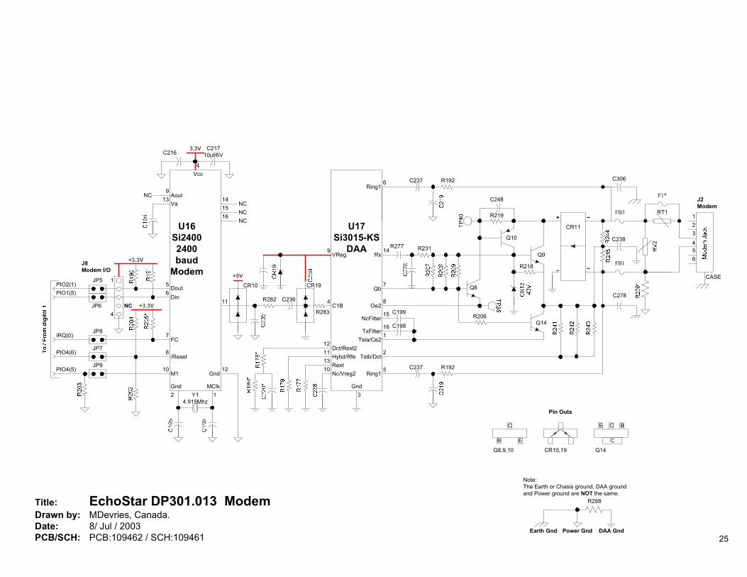
Title: EchoStar DP301.013 ModemDrawn by: MDevries, Canada.Date: 8/ Jul / 2003PCB/SCH: PCB:109462 / SCH:109461
DAA GndPower Gnd
R288
Note:The Earth or Chasis ground, DAA groundand Power ground are NOT the same.
Earth Gnd
U16Si24002400baud
Modem
Y14.915Mhz
C
EB
Pin Outs
C BE
CQ8,9,10 CR10,19 Q14
2Gnd
7FC
56
DinDout
8/Reset
10M1
+3.3V
JP7
JP9
JP8
J8Modem I/O
NC
1
4
JP5
JP6 +3.3V
PIO1(5)PIO2(1)
IRQ(0)
PIO4(6)
PIO4(5)
C216
13Va
9AoutNC F1*
RT1
C278
C306
FB3
FB1
~
~
CR11+
_
Q10
Q9
R219
C248
R218
Q8
R23114R277
Q14
U17Si3015-KS
DAA
7
8
1
4321
56
CASE
J2Modem
1
12Gnd
MClk
CR10+5V
CR19
R282 C236
R283
4
9
11
12111310
Nc/Vreg2
Dct/Rext2
RextHybd/Rfe
Tsta/Ce2
Oe2
Qb
3Gnd
R192C2376
R192C2375Ring1
Ring1
C1B
VReg Rx
C238
R206
2Tstb/Dct
C199
C198
15
16NcFilter
TxFilter
16NC
15NC
14NC
C21710uf/6V
3.3V
Vcc4
25
CR5006
1
2
3
4
5
ISO5001
1
3
+30VdcL50037
12
CR5009~150Vdc
T5001
3
4
R A
TL341
C
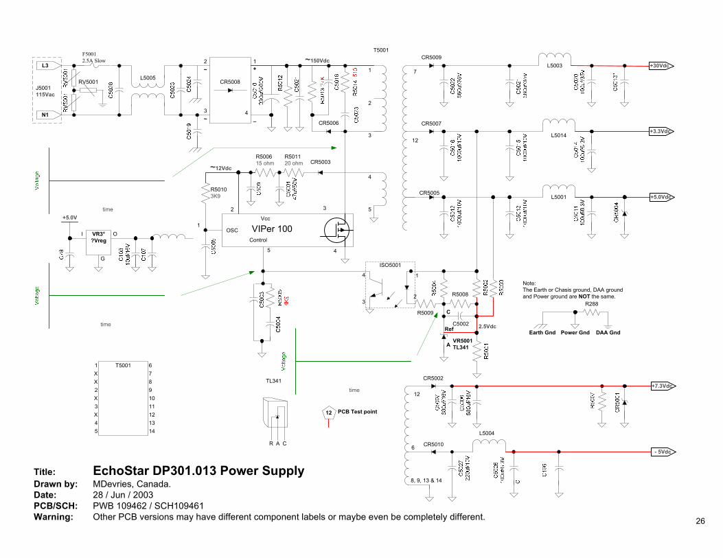
Title: EchoStar DP301.013 Power SupplyDrawn by: MDevries, Canada.Date: 28 / Jun / 2003PCB/SCH: PWB 109462 / SCH109461Warning: Other PCB versions may have different component labels or maybe even be completely different.
F50012.5A Slow
L3
N1
L5005
J5001115Vac
CR5008
12
3 4
RV5001
~
~ +
_
T5001
2
3
45
67891011121314
1XX
X
X
Vcc
OSC VIPer 100Control
5
2
4
R501120 ohm CR5003
R50103K9
~12Vdc
R500615 ohm
12 PCB Test point
C5002
R5008
2.5Vdc
R5009
1
2
VR5001TL341
Ref
C
A
- 5Vdc
8, 9, 13 & 14
CR50106
time
time
time
+3.3VdcL5014
CR5007
CR5005L5001 +5.0Vdc
+7.3Vdc
L5004
12
CR5002
DAA GndPower Gnd
R288
Note:The Earth or Chasis ground, DAA groundand Power ground are NOT the same.
Earth Gnd
+5.0V
VR3*?Vreg
I O
G
26
PQ0R5A1
5V RegVR7
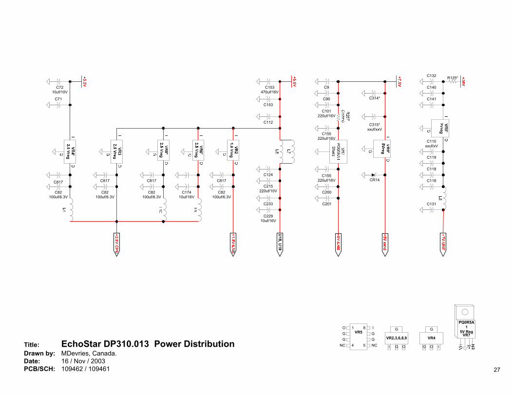
Title: EchoStar DP310.013 Power DistributionDrawn by: MDevries, Canada.Date: 16 / Nov / 2003PCB/SCH: 109462 / 109461
VR5IOGGNC
GG
NC
1
4 5
8
I OG
G
VR2,3,6,8,9
C112
C153470uf/16V
C71
C82100uf/6.3V
C817
C7210uf/10V
C153
C124
C215220uf/10V
C233
C22910uf/16V
C82100uf/6.3V
C817
C82100uf/6.3V
C817
C17410uf/16V
C82100uf/6.3V
C817
C132 R125*
C140
C141
C110xxuf/xV
C119
C118
C118
C131
C155220uf/16V
C90
C101220uf/16V
C9
C155220uf/16V
C200
C201
CR14
C315*xxuf/xxV
C314*
IOG
G
VR4
27
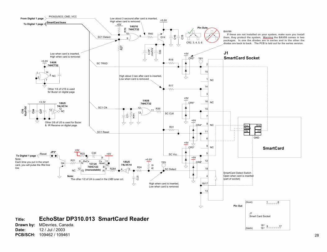
J1SmartCard SocketCR2*
+5V
1
2
3
4
5
6
7
8
9
10
11
12
19/17
14
18
13
15
16 NC
NC
NC
NC
CR5*
+5V
CR4*
+5V
CR3*
+5V
+5.0V
SC CLK
SC Detect
R40
R18
R17
SC Vcc
TP5
R31
1/4U1674HCT32
10
98
1/4U674HCT32
13
1211 R39SC1 Clk
SmartCard
SmartCard Detect SwtichOpen when card is inserted(part of socket)
GND
GndVcc
I/OResetClk
SC1 Detect
SmartCard buss
SC TRXD
Title: EchoStar DP310.013 SmartCard ReaderDrawn by: MDevries, Canada.Date: 12 / Jul / 2003PCB/SCH: 109462 / 109461
To Digital 1 page
Note:Each time you put in the smartcard, you will pulse the /Rst linelow.
To Digital 1 page
Q14
High when card is inserted,Low when card is removed
Low when card is inserted,High when card is removed
High about 3 sec after card is inserted,Low when card is removed
Low about 3 secound after card is inserted,High when card is removed
From Digital 1 page
CR6*
+5V
TP1
Other 1/4 of U16 is usedfor Buzer on digital page
2
13 NC
+5.0V 1/4U674HCT32
14
7
13 12
+3.3V
NC
Other 2/6 of U5 is used for Buzer& IR Receive on digital page.
1/6U574LVC14
SC1 Reset
+5V
+5.0V
R2434
1/6U574LVC14
BAV99 If these are not installed on your system, make sure you installthem, they protect the system, Warning the BAV99 comes in twopackages. In one the diodes are in series and in the other thediodes are back to back. The PCB is laid out for the series version.
Pin Outs
CR2, 3, 4, 5, 6
1 8
1819
9 17
J1Smart Card Socket
Pin Out(front)
(back)
910
5
12
67
C30R33
/AB
Q
/Q
1/2 U474HC123
(monostable)
+5V
reset11
NC
RxCx Cx
+5V
R284
Q4R21
JP3*/Reset
Note: The other 1/2 of U4 is used in the LNB tuner cct.
PIO0(5)/SC0_CMD_VCC
28
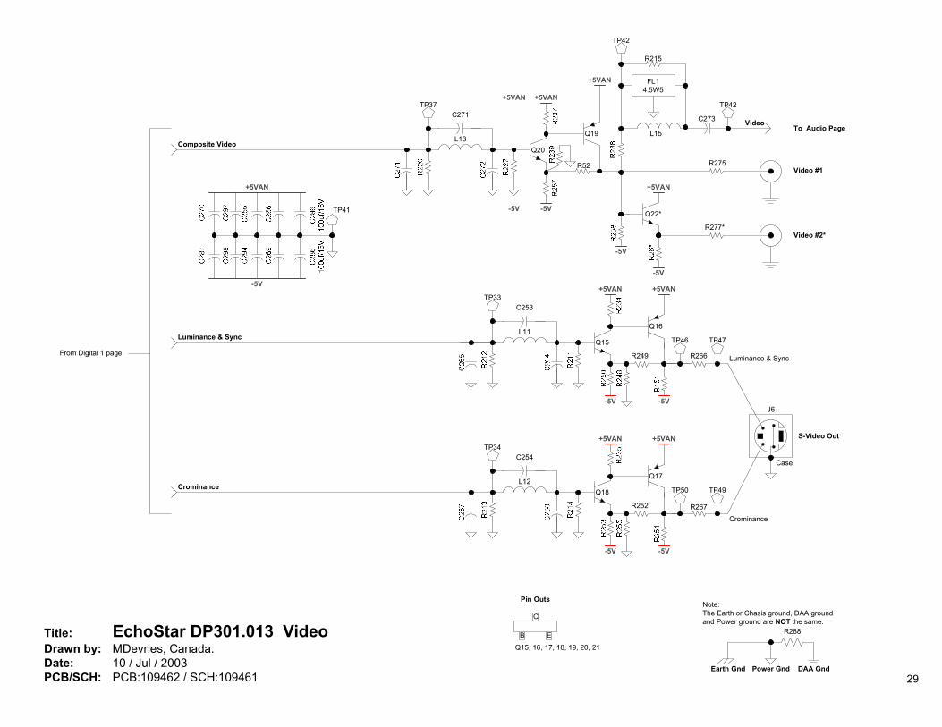
Title: EchoStar DP301.013 VideoDrawn by: MDevries, Canada.Date: 10 / Jul / 2003PCB/SCH: PCB:109462 / SCH:109461
DAA GndPower Gnd
R288
Note:The Earth or Chasis ground, DAA groundand Power ground are NOT the same.
Earth Gnd
J6
Case
S-Video Out
C
EB
Pin Outs
Q15, 16, 17, 18, 19, 20, 21
+5VAN+5VAN
Luminance & Sync
Luminance & Sync TP47
R266
Q16
R249
Q15
+5VAN+5VAN
-5V
L11
C253TP33
-5V
TP46
Crominance
TP49
R267
Q17
R252
Q18
-5V
L12
C254TP34
-5V
Crominance TP50
Video #1R275
R277*Video #2*
Q19
R52
+5VAN
+5VAN
Q22*
FL14.5W5
L15
R215
VideoTo Audio Page
Q20
+5VAN+5VAN
-5V -5V
C273
TP42
TP42
-5V
L13
C271TP37
Composite Video
-5V
-5V
+5VAN
TP41
From Digital 1 page
29
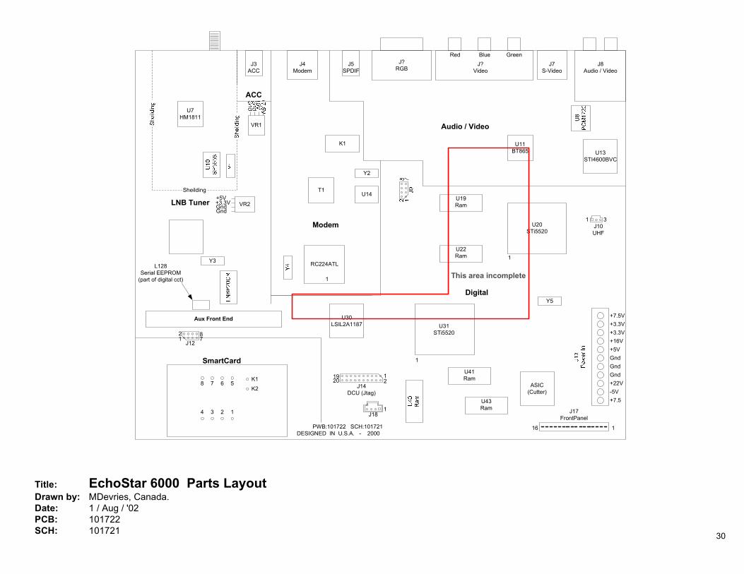
Title: EchoStar 6000 Parts LayoutDrawn by: MDevries, Canada.Date: 1 / Aug / '02PCB: 101722SCH: 101721
Modem
Audio / Video
Digital
RC224ATL
J4Modem
J3ACC
J7S-Video
U20STi5520
J?RGB
J?Video
1
1
LNB Tuner
Aux Front End
SmartCard
1234
5678K1K2
VR1
VR2
T1
K1
ACC
J5SPDIF
BlueRed GreenJ8
Audio / Video
J14DCU (Jtag)
12
1920
1J18
1J10UHF
3
+7.5V+3.3V+3.3V+16V+5VGndGndGnd+22V-5V+7.5
ASIC(Cutter)
U19Ram
U22Ram
U41Ram
U43Ram
116
J17FrontPanel
U31STi5520
1
U13STI4600BVC
U11BT865
Y2
U14
PWB:101722 SCH:101721DESIGNED IN U.S.A. - 2000
U30LSIL2A1187
Y5
Y3
U7HM1811
Sheilding
L128Serial EEPROM
(part of digital cct)
J1212
78
+3.3V+5VGndGnd
This area incomplete
30
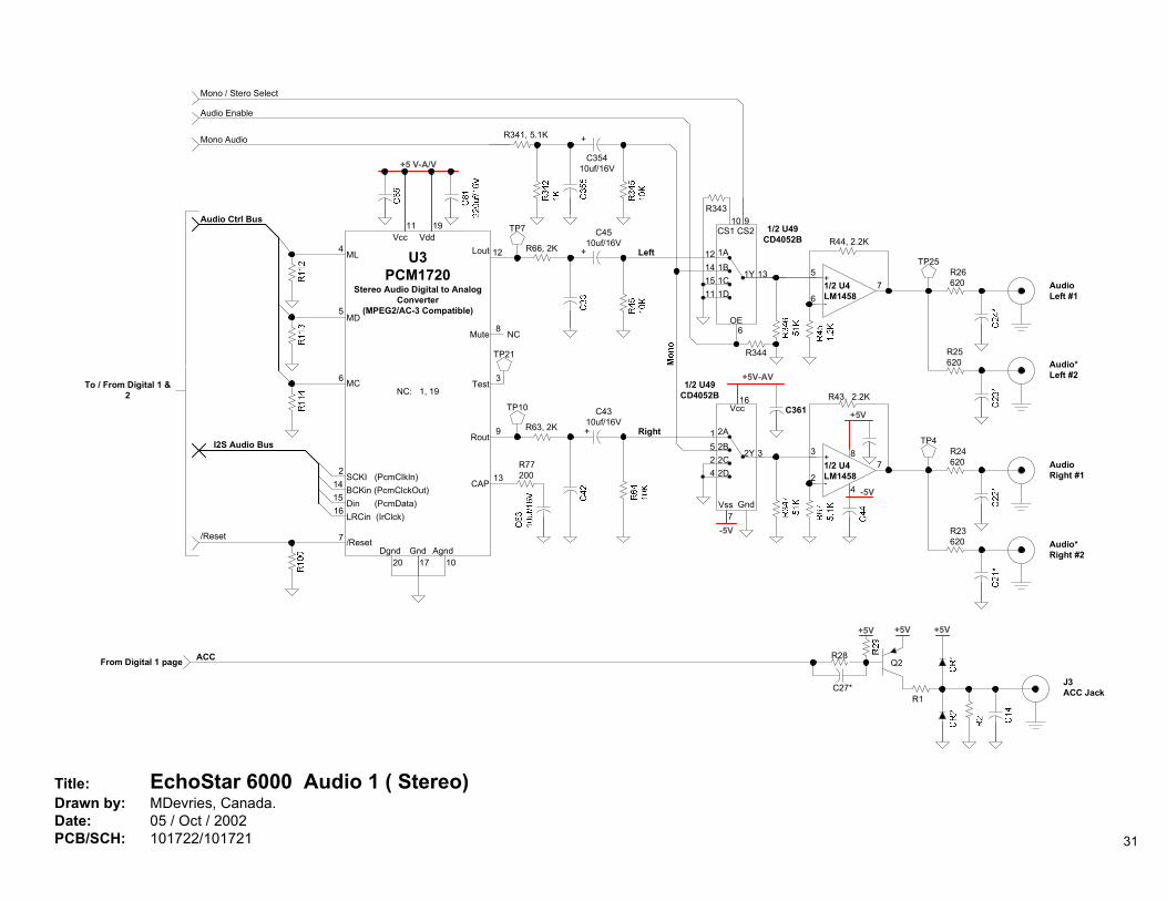
Title: EchoStar 6000 Audio 1 ( Stereo)Drawn by: MDevries, Canada.Date: 05 / Oct / 2002PCB/SCH: 101722/101721
Lout
Rout
Mute
19Vdd
U3PCM1720
Stereo Audio Digital to AnalogConverter
(MPEG2/AC-3 Compatible)
+5 V-A/V
11Vcc
8 NC
9
ML
MD
4
6
C4310uf/16V
TP10
R63, 2K +
NC: 1, 19
1020Dgnd AgndGnd
17
/Reset
CAP 13R77200
Test 3
TP21
MC
5
7
Din (PcmData)BCKin (PcmClckOut)
LRCin (IrClck)
SCKI (PcmClkIn)
1514
16
2
I2S Audio Bus
R44, 2.2K
R26620
R25620
AudioLeft #1
Audio*Left #2
TP25
71/2 U4LM14586
5
-
+
1/2 U49CD4052B
12
1314
1A1B
1Y1511
1C1D
12
C4510uf/16V
TP7
R66, 2K +
R43, 2.2K
R24620
R23620
AudioRight #1
Audio*Right #2
TP4
71/2 U4LM1458
3
2 -
+
4 -5V
+5V
8
1
35
2A2B
2Y24
2C2D
1/2 U49CD4052B
To / From Digital 1 &2
Audio Ctrl Bus
C35410uf/16V
R341, 5.1K +
Left
Right
Gnd7
-5V
Vss
+5V-AV
Vcc C36116
R343
CS1 CS210 9
Mono Audio
Mono / Stero Select
Audio Enable
6OE
R344
/Reset
+5V+5V
C27*
R28Q2
R1
J3ACC Jack
From Digital 1 page ACC
+5V
31
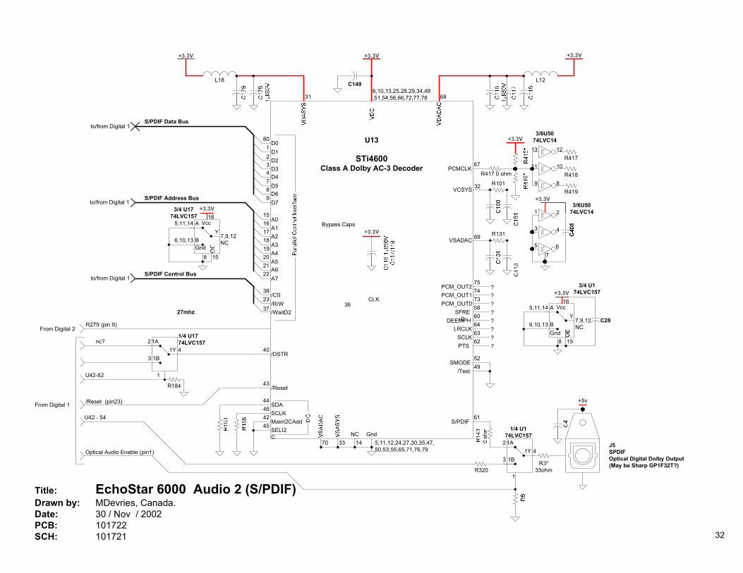
U13
STi4600Class A Dolby AC-3 Decoder
6,10,13,25,28,29,34,48,51,54,56,66,72,77,78
+3.3V
6831
8 15
5,11,14
7,9,12NC6,10,13
A
BY
Vcc
Gnd
+3.3V16
3/4 U1774LVC157
L18 L12
+3.3V
C149
+3.3V
Gnd5,11,12,24,27,30,35,47,50,53,55,65,71,76,79
NC143370
801234789
D0D1D2D3D4D5D6D7
A0A1A2A3A4A5A6A7
1516171819202122
382337
/CS/R/W/WaitD2
S/PDIF Control Bus
S/PDIF Address Bus
S/PDIF Data Busto/from Digital 1
to/from Digital 1
to/from Digital 1
Title: EchoStar 6000 Audio 2 (S/PDIF)Drawn by: MDevries, Canada.Date: 30 / Nov / 2002PCB: 101722SCH: 101721
Optical Audio Enable (pin1)
61S/PDIF
13 12
9 8
11 10
3/6U5074LVC14
R417
R418
R419
67PCMCLK
R417 0 ohm
1 2
5 6
3 4
7
+3.3V3/6U50
74LVC14
8 15
5,11,14
7,9,12NC6,10,13
A
BY
Vcc
Gnd
+3.3V
C28
16
3/4 U174LVC157
DEEMPH60
?SFRE
Q
58?
44SDA
46SCLK
42MainI2CAdd
45SELI2C
PCM_OUT073
?
74?
75?
PCM_OUT1PCM_OUT2
R10132
R13169
VCSYS
VSADAC
52SMODE
49/Test
PTS62
?
63?
64?
SCLKLRCLK
27mhz36
CLK
/Reset
/Reset (pin23)
43
From Digital 1
From Digital 2R279 (pin 9)
+3.3VBypass Caps
+3.3V
+5v
J5SPDIFOptical Digital Dolby Output(May be Sharp GP1F32T?)R3*
33ohm
1/4 U174LVC157
24
3
1A
1B1Y
U42 - 54
1
R184
1/4 U1774LVC15724
3
1A
1B1Y
1
40/DSTR
U42-62
nc?
R320
32
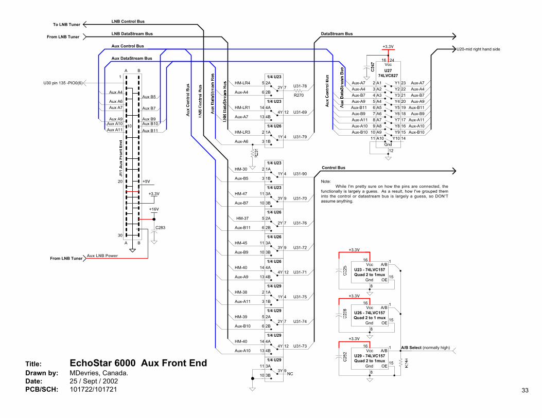
Title: EchoStar 6000 Aux Front EndDrawn by: MDevries, Canada.Date: 25 / Sept / 2002PCB/SCH: 101722/101721
From LNB Tuner
To LNB Tuner
From LNB Tuner
LNB Control Bus
LNB DataStream Bus
Aux Control Bus
Aux DataStream Bus
1
10
20
30
A B
A B
+3.3V
Aux B5Aux A4
Aux B7Aux A7Aux A6
Aux B11
Aux A9 Aux B9
Aux A11Aux B10Aux A10
Aux LNB Power
+16V
C283
U30 pin 135 -PIO0(6)
+5V
Control Bus
DataStream Bus
12
U2774LVC827
A1A2A3A4A5A6A7A8A9A10
Y1Y2Y3Y4Y5Y6Y7Y8Y9
Y10
23456789
1011
23222120191817161514
Gnd
Vcc2416
+3.3V
HM-37
Aux-B11
HM-45
Aux-B9
HM-40
Aux-A9
HM-38
Aux-A11
Aux-B10
HM-39
HM-40
Aux-A10
HM-30
Aux-B5
HM-47
Aux-B7
1/4 U265
76
2A
2B2Y
1/4 U2611
910
3A
3B3Y
1/4 U2614
1213
4A
4B4Y
1/4 U292
43
1A
1B1Y
1/4 U295
76
2A
2B2Y
1/4 U2911
910
3A
3B3Y
1/4 U2914
1213
4A
4B4Y
1/4 U232
43
1A
1B1Y
1/4 U2311
910
3A
3B3Y
NC
Aux-B11Aux-B9
Aux-A9
Aux-A11
Aux-B10Aux-A10
Aux-B7Aux-A4Aux-A7
U20-mid right hand side
Aux-B11Aux-B9
Aux-A9
Aux-A11
Aux-B10Aux-A10
Aux-B7Aux-A4Aux-A7
U31-70
U31-76
U31-72
U31-71
U31-75
U31-74
U31-73
U31-90
Aux-A6
HM-LR4
Aux-A4
HM-LR1
Aux-A7
HM-LR31/4 U26
24
3
1A
1B1Y
1/4 U235
76
2A
2B2Y
1/4 U2314
1213
4A
4B4Y U31-69
U31-79
U31-78
R270
Note: While I'm pretty sure on how the pins are connected, thefunctionally is largely a guess. As a result, how I've grouped theminto the control or datastream bus is largely a guess, so DON'Tassume anything.
A/B Select (normally high)16
+3.3V
U29 - 74LVC157Quad 2 to 1mux
Vcc
8
15
A/B
OE
1
Gnd
16
+3.3V
U26 - 74LVC157Quad 2 to 1 mux
Vcc
8
15
A/B
OE
1
Gnd
16
+3.3V
U23 - 74LVC157Quad 2 to 1mux
Vcc
8
15
A/B
OE
1
Gnd
33
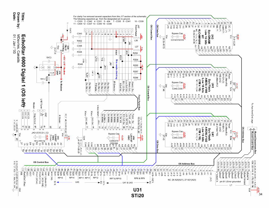
NC: 26 A20(A21), 27 A21(A23)
OS Control Bus
L?
pin 81 LError grounded
OS Address Bus
Bypass Cap
C314/315/316
Bypass Cap
C346,C330
Bypass Cap
C346,C330
U41 & U43
RP7 & RP10 RP6 & RP9RP11 RP12
U45
RP15 RP14 RP11
Bypass Cap
C295/270/255/266
R402
R348
R348
C343
C348 L27
L26
R294
R295
R297
R304
R296
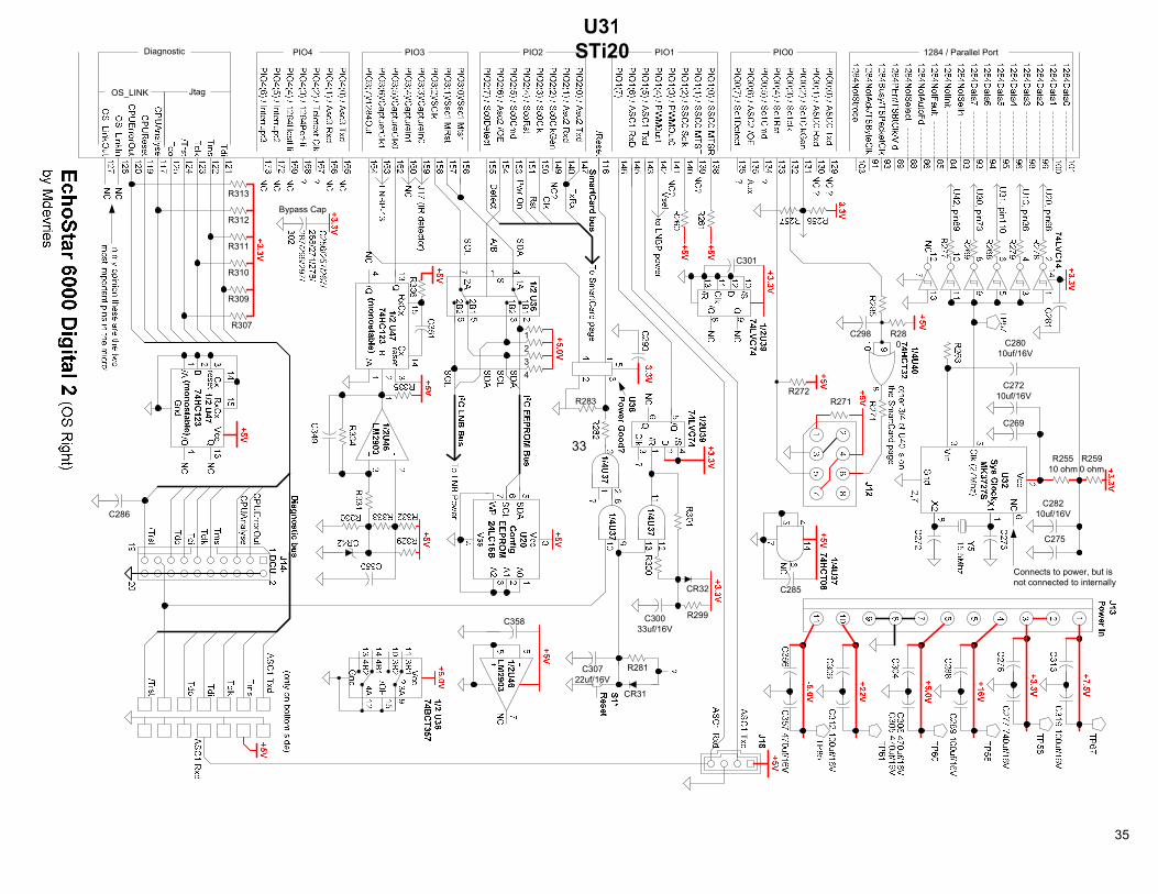
U31STi20
For clarity I've removed several capacitors from this J17 section of the schematic.The following capacitors go from the designated pin to ground. 1 - C333 2 - C342 4 - C331 5 - 404 7 - C335 9 - C341 10 - C33911 - C404 12 - C337 13 - C340 16 - C336
34
C301
C285
U31STi20PIO2
C358
PIO4 1284 / Parallel PortPIO3 PIO1Diagnostic
JtagOS_LINK
R307
R309
R310
R311
R312
R313
C286
Bypass Cap
PIO0
CR32
R299C30033uf/16V
R281C30722uf/16V
CR31
R283
C28010uf/16V
R25510 ohm
C27210uf/16V
C269
Connects to power, but isnot connected to internally
C275
C28210uf/16V
R2590 ohm
R271
C298 R280
R272
1234
33
35
Vdd
+3.3V
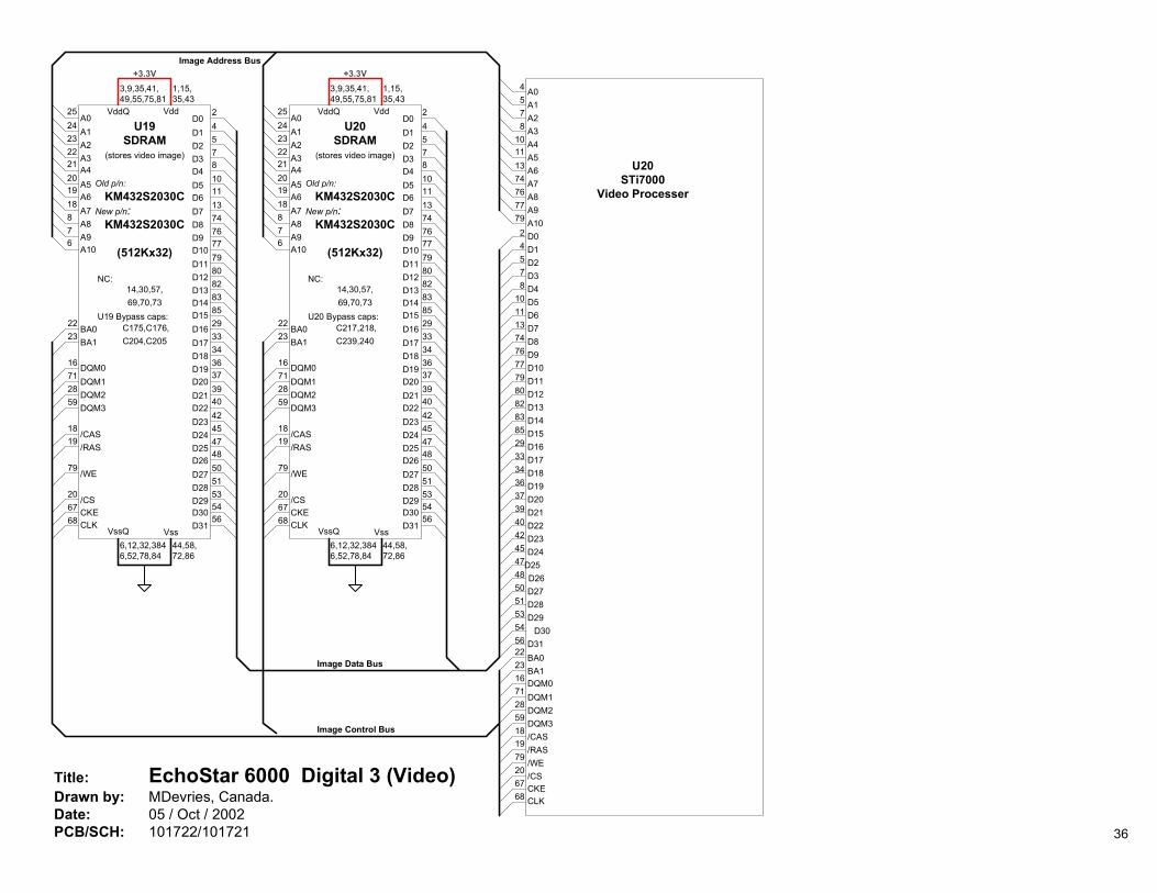
U20SDRAM
(stores video image)
Old p/n:KM432S2030C
New p/n:KM432S2030C
(512Kx32)
NC:14,30,57,69,70,73
U20 Bypass caps: C217,218,C239,240
245781011137476777980828385
D0D1D2D3D4D5D6D7D8D9D10D11D12D13D14D15
A9
1,15,35,43
29333436373940424547485051535456
D16D17D18D19D20D21D22D23D24D25D26D27D28D29D30D31
Vss44,58,72,86
VddQ
3,9,35,41,49,55,75,81
VssQ6,12,32,3846,52,78,84
A0A1A2A3A4A5A6A7A8
A10
2524232221201918876
/CAS/RAS
/WE
/CSCKECLK
1819
79
6768
20
BA0BA1
2223
DQM0DQM1DQM2DQM3
16712859
Vdd
+3.3V
U19SDRAM
(stores video image)
Old p/n:KM432S2030C
New p/n:KM432S2030C
(512Kx32)
NC:14,30,57,69,70,73
U19 Bypass caps: C175,C176,C204,C205
245781011137476777980828385
D0D1D2D3D4D5D6D7D8D9D10D11D12D13D14D15
A9
1,15,35,43
29333436373940424547485051535456
D16D17D18D19D20D21D22D23D24D25D26D27D28D29D30D31
Vss44,58,72,86
VddQ
3,9,35,41,49,55,75,81
VssQ6,12,32,3846,52,78,84
A0A1A2A3A4A5A6A7A8
A10
2524232221201918876
/CAS/RAS
/WE
/CSCKECLK
1819
79
6768
20
BA0BA1
2223
DQM0DQM1DQM2DQM3
16712859
24578
101113747677798082838529333436373940424547485051535456
D0D1D2D3D4D5D6D7D8D9D10D11D12D13D14D15D16D17D18D19D20D21D22D23D24
D25D26D27D28D29
D30D31
A0A1A2A3A4A5A6A7A8A9A10
4578
10111374767779
BA0BA1
2223
DQM0DQM1DQM2DQM3
16712859
/CAS/RAS
1819
/WE79
/CSCKECLK
6768
20
Image Address Bus
Image Data Bus
Image Control Bus
U20STi7000
Video Processer
Title: EchoStar 6000 Digital 3 (Video)Drawn by: MDevries, Canada.Date: 05 / Oct / 2002PCB/SCH: 101722/101721 36
14,21,41,54
26,55
+3.3V
VccioVccint
+3.3V
3,37
1-31-4
1-10
1-6
1-151-14/GClk31-23
1-27
1-2
1-5
1-8
1-11/GClk2
1213
18
10
191723
20
8
9
11
16
1-9/GClk115
?
?Hsync
?
??
Video HiDef
1/4 RP17*
1/4 RP17*
U12Bypass Caps
+3.3VC139,C148,C159,C162
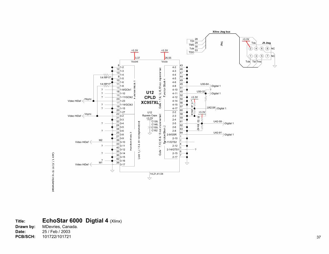
U12CPLD
XC957XL
2-32-4
2-9/GSR
2-6
2-14/GTS12-12
2-11/GTS2
2-15
2-2
2-5
2-8
2-10
5859
64
62
542
6
60
61
63
1
2-177
?
+3.3V
U42-59Digital 1
U42-91Digital 1
3-33-4
3-10
3-6
3-153-143-12
3-16
3-2
3-5
3-8
3-11
3132
39
34
363540
42
22
24
25
33
?
3-927
3-1738
?
?
?
VsyncVideo HiDef
?
M2Video HiDef
M1Video HiDef
4-34-4
4-10
4-6
4-154-144-12
4-17
4-2
4-5
4-8
4-11
4647
51
49
565052
57
43
44
45
48
+3.3V
U30-64Digital 1
Digital 1U30-32
U42-54 Digital 1
?
Tclk Tdi
Tdo
Tms
NC
NC
Xilinx Jtag bus
J9 Jtag
2
1
4
3
6
5
8
7
+3.3V
Tclk53
TDI28
TDO
3029
TMS
Title: EchoStar 6000 Digtial 4 (Xlinx)Drawn by: MDevries, Canada.Date: 25 / Feb / 2003PCB/SCH: 101722/101721 37
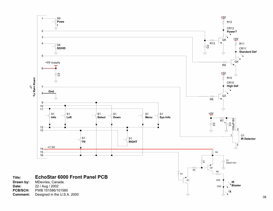
Title: EchoStar 6000 Front Panel PCBDrawn by: MDevries, Canada.Date: 22 / Aug / 2002PCB/SCH: PWB 101586/101585Comment: Designed in the U.S.A. 2000
CR12Power?
R12
Q5R13
+5V
15
1213
14
CR11Standard Def
R11
Q4R9
+5V
CR10High Def
R10
Q3R6
+5V
R7+
U1IR Detector
2
3
1
+5V
IRBlaster
CR9
CR8
Q1
R1
R2Q2
C1300uF/16V
R4
R6
1516
2
1 S9Power
4 S8SD/HD
3
5
+5V supply
6
7
8
11109
S1Info
S1Up
S1Select
S1Down
S1RIGHT
S1Menu
S1Left
S1Sys Info
+7.5V
Gnd
38
L17unkownvoltage
+3.3V RF
LR1LR2LR3LR4
To Aux Front End Transport Data Stream
FBClkFDataFErrorFDValid
48363533
C165
C14698
94
U18like butNOT a
HM1211
959697
???
+5V RF
83
82
81
PLL Enable
PLL Data
PLL Clock
R206
Y310.11Mhz
C223
I2C BusTo Digital 2
4950
DataClock
ResetPIO3(5)To Digital 2
+5V RF
A0A1A2A3A4A5A6
24
23 Xtal
Xtal
Gnd 15
U6SP5658SLNB PLL
4
5
6
Enable
Data
ClockRef
C123
100ohm
2
3
13C122 R116
14
Drive
Charge Pump C135
R134C137
1
16 Q9
11
+5V LNB
12
100ohm
100ohm
R133
LNB Power 13/18 V
U7HM1811
NC:
C35 717
C34 616
C47 914
C46 815
C84 3132
C84 2425
2628
C70
C71
R78
R79 R97
R80
+5V RF
+5V RF
39
38
?
?
4647?
?
?+5V RFR6748
uLine
C7C36 R4 R6Q1
10 C1
Rf
34 CR6
+5V RF
+5V RF1,2,25,36
?R132
18
19?
R120
+5V RF (U7 Bypass caps)
LNB
Sheild
R165
R157
Sheild
Sheild Sheild
+Vin+Vout
GndOn/Off
VR 1&2 Pin out
+3.3V RF
+5VVR2
PQ3RD083
+5V RF
+7.5V
L16VR1
PQ05RA1
+16V
+22VU25 Bypass Caps
78
79
35
13,37GND
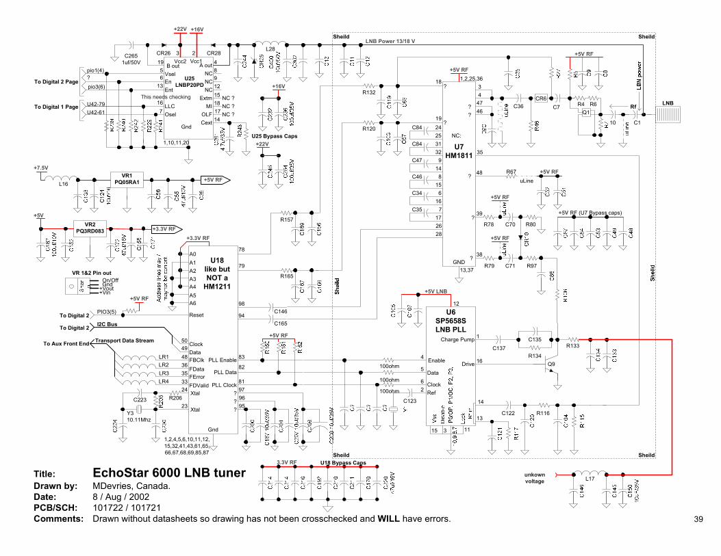
Title: EchoStar 6000 LNB tunerDrawn by: MDevries, Canada.Date: 8 / Aug / 2002PCB/SCH: 101722 / 101721Comments: Drawn without datasheets so drawing has not been crosschecked and WILL have errors.
3.3V RF U18 Bypass Caps
1,2,4,5,6,10,11,12,15,32,41,43,61,65,66,67,68,69,85,87
L28
U25LNBP20PDTo Digital 2 Page En
LLC
Vsel
Osel
Ent
7
5
13
16
pio3(6)
19 Vcc1
Gnd
CR28
1,10,11,20
4
+22V
Vcc2A outB out
2
+16V
3
NCNCNC
912
86
CR26C2651uf/50V
18
Cext
15Extm NC ?MI NC ?
1417OLF NC ?
pio1(4)
U42-61To Digital 1 Page U42-79
This needs checking
?
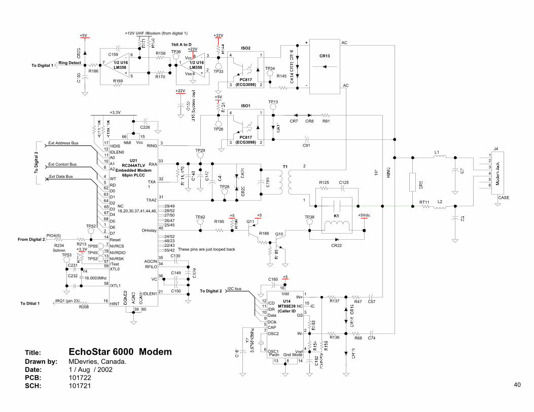
39
Title: EchoStar 6000 ModemDrawn by: MDevries, Canada.Date: 1 / Aug / 2002PCB: 101722SCH: 101721
1
6
5 4
3
2
8
Vss
Vcc
+
-
+
-
+22V
+22V+5V
7
TP36
R170
R158
1/2 U16LM358
1/2 U16LM358
R186
R169
1bit A to D
Ring DetectTo Digital 1
R20816
HINTTo Ditial 1 IRQ1 (pin 23)
R213From Digital 2
PIO4(5)
15
+5VdcTP38
Ext Contorl Bus
OHrelay
RING
Ext Data Bus
U21RC244ATLV
Embedded Modem68pin PLCC
WTRD62
636465676812
45
14
40
3
108
11
NC18,20,30,37,41,44,46,
A0A1A2
D0D1D2D3D4D5D6D7
CR22
C125R125
4321
56
CASE
J4
T1
1
2RXA
TXA1
TXA2
33
32
31
Q10R188
+3.3V
VccNMIHDIS
+5+5R195 Q11
TP28
17
IDLEN0
66
12
29/4928/5227/5026/4725/45
24/5248/2322/4355/42
Reset
C231
C232 16.0003MhzY4
These pins are just looped backTP53
/Test57
+3.3VTP45TP55
TP52
39 60
Ext Address Bus
NVRDIONVRSK
NVRCS1913
7
XTL0
/XTL1
59
58
TP52
K1TP42
R2340ohmn
C226
L1
L2RT11
IDLEN1
C149
C150
VC
C130
21
RFILOAGCIN
36
3435
PC817(ECG3098)
ISO24
3 2
1
R145
+
-
AC
AC
TP34
CR13
TP33
PC817(ECG3098)
ISO14
3 2
1
R81
TP26
+5V
TP29
To Digital 2
DClk9
1110
12 /CD/DRData
I2C bus
CAP5
U14MT88E39(Caller ID
+5
Vdd
C160
16
IN+
Vref
IN-2
3
4
1
GS
R137
R136 R68
R47
C74
C57NC IC
15
OSC1
OSC2
6
7
14Gnd
8Pwdn Mode
13
+22V
CR8CR7
TP13
C91
C159
+12V UHF /Modem (from digital 1)
40
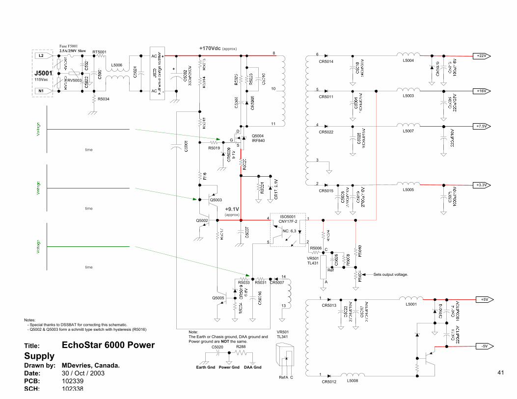
Title: EchoStar 6000 PowerSupplyDrawn by: MDevries, Canada.Date: 30 / Oct / 2003PCB: 102339SCH: 102338
8
11
D
GS
R5019
Q5005
14
13
CR5007R5031R5033
Q5004IRF840
+7.5VL5007
4
CR5022
+3.3VL5005
2
CR5015
+22VL5004
6
CR5014
+16VL5003
5
CR5011
3
10
+170Vdc (approx)
ISO5001CNY17F-2
14
5 2
NC: 6,3
+9.1V(approx)
-
+
Fuse F50012.5A/250V Slow
L2
N1
L5006
J5001115Vac RV5003
RT5001AC
AC
R5034
DAA GndPower Gnd
R288
Note:The Earth or Chasis ground, DAA ground andPower ground are NOT the same.
Earth Gnd
C5020
RefA
VR501TL341
C
+
+5VL5001
1
CR5013
-5V
L50081
CR5012
R5006
Sets output voltage.
A
C
Ref
VR501TL431
Q5003
Q5002
Notes: - Special thanks to DSSBAT for correcting this schematic. - Q5002 & Q5003 form a schmitt type switch with hysteresis (R5016)
time
time
time
41
J15SmartCard SocketCR33*
+5V
1
2
3
4
5
6
7
8
9
10
11
12
13
14
37
34
15
16 NC
NC
NC
NC
CR22*
+5V
CR35*
+5V
CR36*
+5V
+5V
SC CLK
SC Detect
R323
R318
R325
SC Vcc
TP84+5V
R338
R319
Q12
12
1/6U4874HCT14
1 2
5 6
3 4
7
+5V
1/4U4074HCT32
2
13
1/4U4074HCT32
5
46
56
1/6U4874HCT14
34
1/6U4874HCT14
C360*
+5V
R317SC1 Clk (PIO2-3)
SC1 Reset (PIO2-4)
SmartCard
SmartCard Detect Switch isclosed when card is inserted(part of socket)
GND
GndVcc
I/OResetClk
SC1 Detect (PIO2-7)
13
1211 NC
+5V 1/4U4074HCT32
14
7
SmartCard buss
SC TRXD (PIO2-0/1)
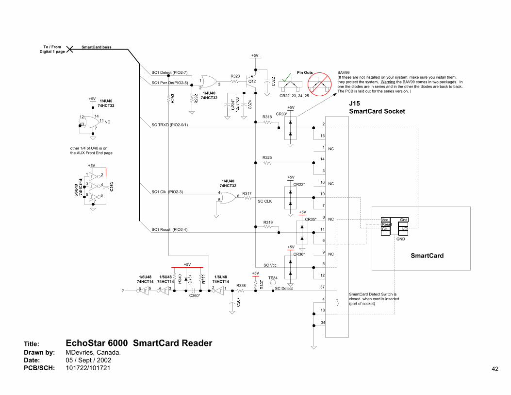
Title: EchoStar 6000 SmartCard ReaderDrawn by: MDevries, Canada.Date: 05 / Sept / 2002PCB/SCH: 101722/101721
other 1/4 of U40 is onthe AUX Front End page
To / FromDigital 1 page
?
SC1 Pwr On(PIO2-5)
BAV99(If these are not installed on your system, make sure you install them,they protect the system, Warning the BAV99 comes in two packages. Inone the diodes are in series and in the other the diodes are back to back.The PCB is laid out for the series version. )
Pin Outs
CR22, 23, 24, 25
42
R9
+5V-A/V
Q3R30
R11
+5V-A/V
Q4R31
V-Sync
H-Sync
J6RGB Video(VGA)
Green
Blue
11/2 U6AD8283
2 -
+
R52
R86 R87
C76R88
R55
-5V C39
4
CR44
nc
37Vref
V-Sync
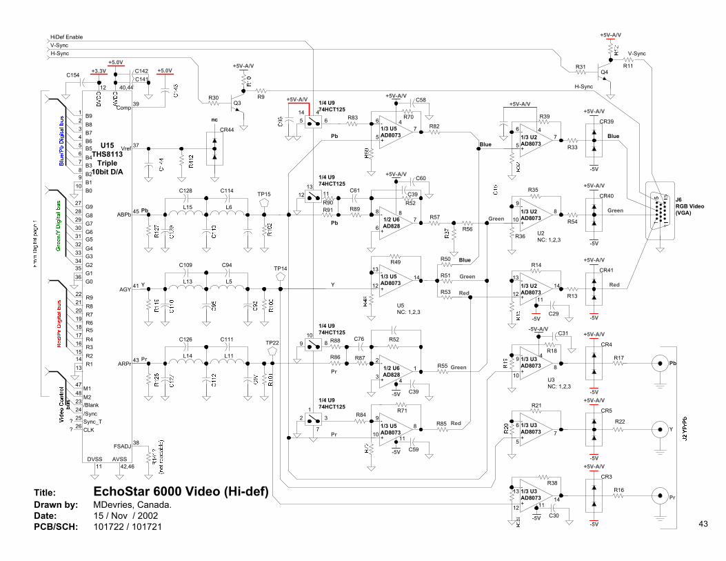
Title: EchoStar 6000 Video (Hi-def)Drawn by: MDevries, Canada.Date: 15 / Nov / 2002PCB/SCH: 101722 / 101721
CR41
+5V-A/V
-5V
Red141/3 U2AD807312
13 -
+
R14
R13
-5VC29
11
CR40
+5V-A/V
-5V
Green81/3 U2AD807310
9 -
+
R36
R35
R54
U2NC: 1,2,3
Blue
CR39
+5V-A/V
-5V
71/3 U2AD80735
6 -
+
R39
R33
+5V-A/V
4
Y
PrR16
CR3
+5V-A/V
-5V
141/3 U3AD8073
12
13-
+
R38
-5V C30
11
81/3 U5AD807310
9 -
+
R84R71
R85 Red
-5V C59
11
R51
R53
R50
141/3 U5AD807312
13 -
+
R49
Red
Blue
Green
R5671/2 U6
AD8286
8 -
+
R52C39
R91 R89
C61
R90
R57
+5V-A/VC60
8
71/3 U5AD80735
6 -
+
R83 R70R82
+5V-A/VC58
4
45ABPb
C114
L6
C128
L15Pb
TP15
C94
L5
C109
L13
TP14
C111
L11
C126
L14
TP22
PbR17
CR4
+5V-A/V
-5V
81/3 U3AD8073
10
9-
+
R18
U3NC: 1,2,3
-5V-A/VC31
4
CR5
+5V-A/V
-5V
R22
71/3 U3AD8073
5
6-
+
R21
U5NC: 1,2,3
DVSS11
AVSS42,46
U15THS8113
Triple10bit D/A
38FSADJ
41AGYY
43ARPrPr
R9R8R7R6R5R4R3R2R1
22212019181716151413
G9G8G7G6G5G4G3G2G1G0
27282930313233343536
47
M2M1
48
/Sync/Blank23
24
CLKSync_T25
26??
B9B8B7B6B5B4B3B2B1B0
123456789
10
12
+3.3VC154
40,44
+5.0V
39Comp
+5.0VC141C142
Pb
Pb
Y
Pr
Pr
Green
+5V-A/V
HiDef Enable
65
1/4 U974HCT125414
1112
1/4 U974HCT12513
89
1/4 U974HCT12510
32
1/4 U974HCT1251
7
H-Sync
43
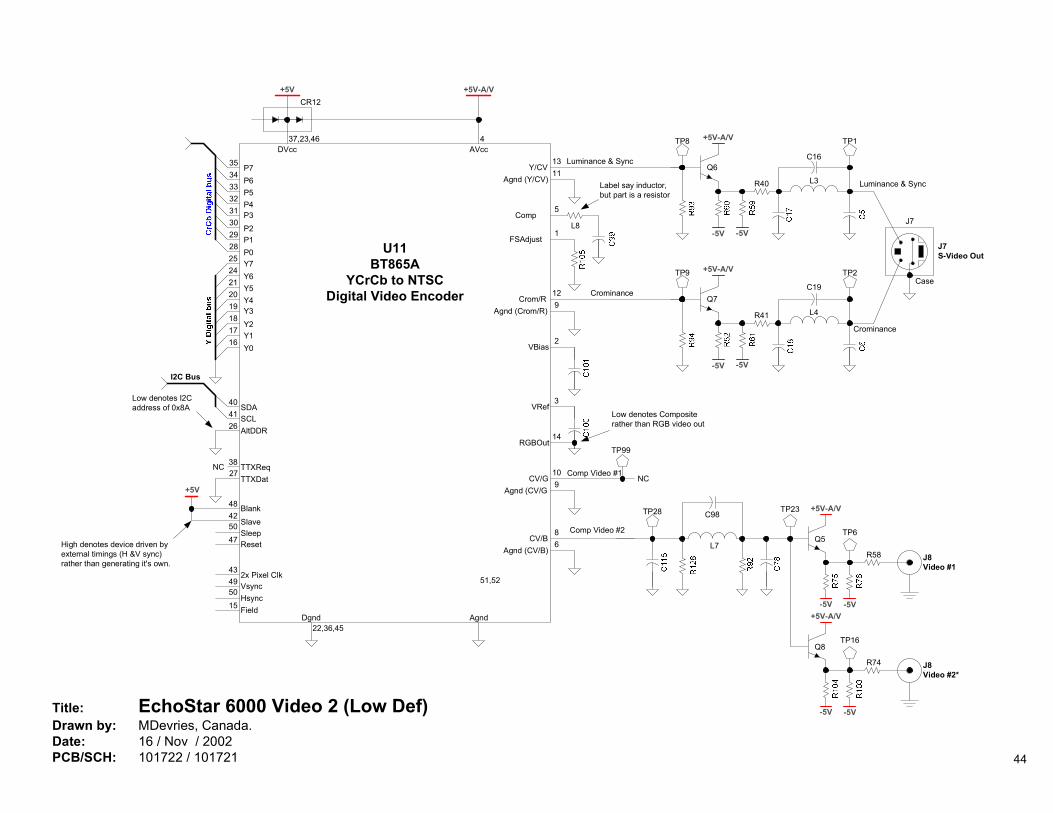
Title: EchoStar 6000 Video 2 (Low Def)Drawn by: MDevries, Canada.Date: 16 / Nov / 2002PCB/SCH: 101722 / 101721
R41 L4
C19Q7
+5V-A/V
-5V -5V
Luminance & Sync
Crominance
TP2
J7
Case
J7S-Video Out
TP9
Luminance & Sync
TP1
R40 L3
C16Q6
+5V-A/V
-5V -5V
TP8
Crominance
U11BT865A
YCrCb to NTSCDigital Video Encoder
Y7Y6Y5Y4Y3Y2Y1Y0
2524212019181716
P7P6P5P4P3P2P1P0
3534333231302928
+5V-A/V+5V
DVcc AVcc
51,52
37,23,46 4
1FSAdjust
SDASCL
4041
I2C Bus
Y/CV1311
Agnd (Y/CV)
12Crom/R
9Agnd (Crom/R)
2VBias
TP23
R74 J8Video #2*
+5V-A/V
Q8TP16
-5V-5V
R58 J8Video #1
+5V-A/V
Q5TP6
-5V-5V
C98
L7
TP28
Comp Video #28CV/B
6Agnd (CV/B)
3VRef
TP99
Comp Video #110CV/G
9Agnd (CV/G
NC
14RGBOut
Low denotes Compositerather than RGB video out
Low denotes I2Caddress of 0x8A
5Comp
L8
Label say inductor,but part is a resistor
TTXReq38
TTXDat27
NC
AltDDR26
Dgnd Agnd22,36,45
2x Pixel Clk43
Vsync49
Hsync50
Field15
High denotes device driven byexternal timings (H &V sync)rather than generating it's own.
Reset47Sleep
50 Slave42
+5V
Blank48
CR12
44
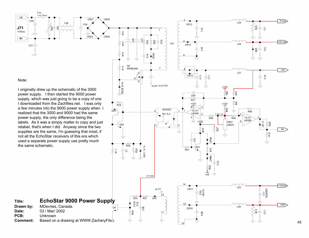
Title: EchoStar 9000 Power SupplyDrawn by: MDevries, Canada.Date: 03 / Mar/ 2002PCB: UnknownComment: Based on a drawing at WWW.ZacheryFiles
+22 VdcL04
4
6
-5 VdcL022
CR14
CR12
+5VL01
8
CR13
CR01 CR02
CR03 CR04
Fuse1.6A Slow
C24
L2
N1
C22
C21
L06
J71115Vac 1
7
D
GS
14 +12VdcL03
CR11
+30VL05
12
10
CR16
ISO500114
5 2
3
21
+
-
1/2 U1LM358
8
46
57
+
-
1/2 U1LM358
R08
PF
+12V
2.5V refR08
+12VR11
C06
R04
R07
+12V VR01LM431
+12V
Q01
+5V
NC: 6,3
R20
13
11
CR7R31R33
Q5
Q4IRFBE30D
R16
Q03
Q02
+17.5V
Note:
I originally drew up the schematic of the 3000power supply. I then started the 9000 powersupply, which was just going to be a copy of oneI downloaded from the Zachfiles.net. I was onlya few minutes into the 9000 power supply when Irealized that the 3000 and 9000 had the samepower supply, the only difference being thelabels. As it was a simply matter to copy and justrelabel, that's when I did. Anyway since the twosupplies are the same, I'm guessing that most, ifnot all the EchoStar receivers of this era whichused a separate power supply use pretty muchthe same schematic.
T01
to pin 13 of T01
to C?
45
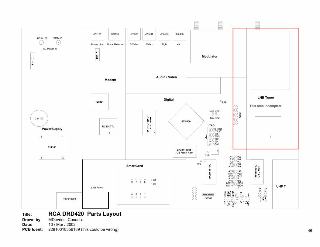
Title: RCA DRD420 Parts LayoutDrawn by: MDevries, Canada.Date: 10 / Mar / 2002PCB Ident: 22910018356189 (this could be wrong)
PowerSupply
ModemAudio / Video
Digital
Modulator
SmartCard
UHF ?
LNB Tuner
T14100
C14107
RC224ATL
T28101
BC14100 BC14101
AC Power in
L N
J28101 J29103 J22407 J22404 J22406 J22405
STi5500
15
6 10
LeftRightVideoS-Video
1234
5678K1K2
GndTDO
TCKTMSTDI/TRSTS_RST
JTAG
A20
A9A8A7A6A5
MD13
OEA15
A13A11
MD15
A19
A10A1A2A3A4
MD12A16A14A12A18
MD14
J33501
LH28F160S5TOS Flash Rom
Power good
Gnd Gnd
TX2 RX2
Phone Line Home Network
BFR
FCE
LNB Power
FP21
1
1
1
1
1
11
This area incomplete
46
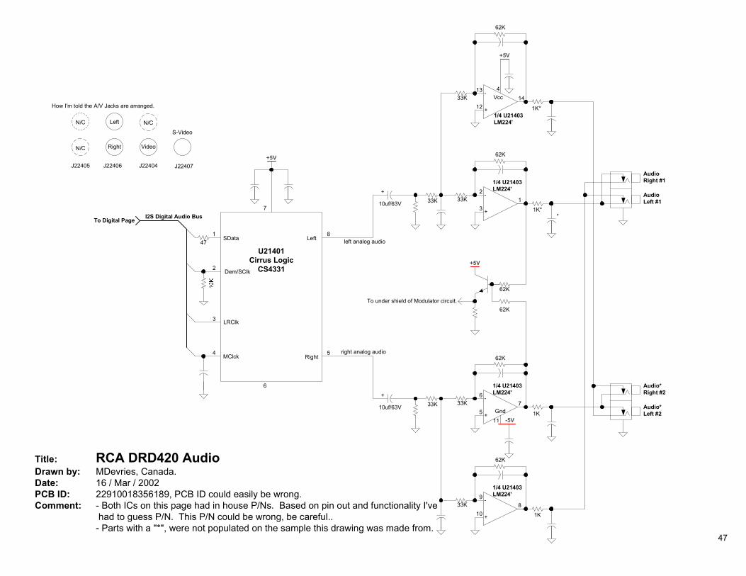
Title: RCA DRD420 AudioDrawn by: MDevries, Canada.Date: 16 / Mar / 2002PCB ID: 22910018356189, PCB ID could easily be wrong.Comment: - Both ICs on this page had in house P/Ns. Based on pin out and functionality I've
had to guess P/N. This P/N could be wrong, be careful..- Parts with a "*", were not populated on the sample this drawing was made from.
62K
1412
13 -
+ 1K*
1K*
1/4 U21403LM224'
33K
62K
13
2 -
+
1/4 U21403LM224'
33K+
33K10uf/63V
U21401Cirrus Logic
CS4331
I2S Digital Audio BusTo Digital Page
4 MClck
LRClk
Dem/SClk
SData
3
2
147
7
6
Left
Right5
8
+5V
62K
75
6 -
+ 1K
1K
1/4 U21403LM224'
33K
62K
810
9 -
+
1/4 U21403LM224'
33K
+33K10uf/63V
Vcc4
-5VGnd
11
*
+5V
left analog audio
right analog audio
Left
Right Video
S-Video
J22405 J22406 J22404 J22407
N/C
N/C
N/C
How I'm told the A/V Jacks are arranged.
Audio*Right #2
Audio*Left #2
To under shield of Modulator circuit.
62K
62K
+5V
AudioRight #1
AudioLeft #1
47
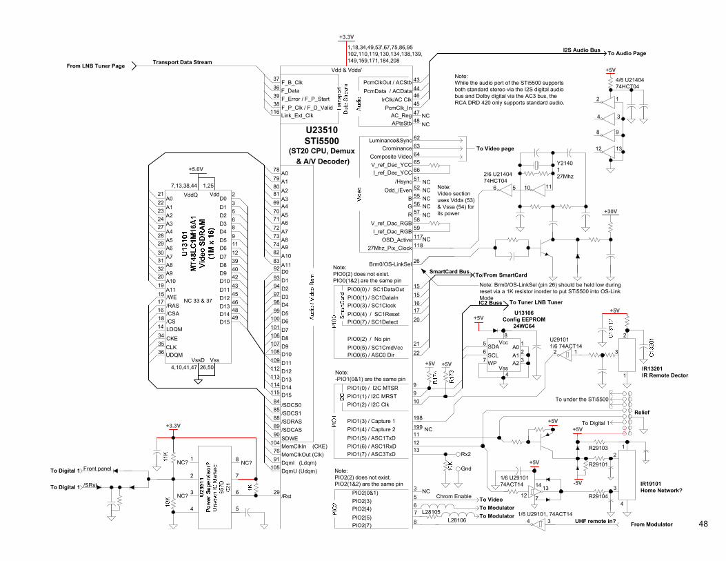
U23510STi5500
(ST20 CPU, Demux & A/V Decoder)
A0A1A2A3A4A5A6A7A8A9A10A11
212223242728293031322019
Vdd
+5.0V
NC 33 & 37
23568911123940424345464849
D0D1D2D3D4D5D6D7D8D9D10D11D12D13D14D15
1517161814
/WE/RAS/CSA/CSLDQM
1,257,13,38,44VddQ
26,504,10,41,47VssVssD
D0D1D2D3D4D5D6D7D8D9D10D11D12D13D14D15
929394979899
100101106107108109112113114115
787980
6970717273748283
81
A0A1A2A3A4A5A6A7A8
A10A11
A9
CKECLKUDQM
343536
/SDCS0/SDCS1
/SDCASSDWE
8485888990
/SDRAS
MemClkIn (CKE)MemClkOut (Clk)
DqmU (Udqm)
1047691
105Dqml (Ldqm)
+3.3V
37363938
116
F_B_ClkF_DataF_Error / F_P_StartF_P_Clk / F_D_ValidLink_Ext_Clk
Transport Data StreamFrom LNB Tuner Page
3567
PIO2(0&1)
8PIO2(5)PIO2(4)PIO2(3)
Note:PIO2(2) does not exist.PIO2(1&2) are the same pin
PIO2(7)
To Video page
117118
OSD_Active27Mhz_Pix_Clock
/HsyncOdd_/Even
RG
515255565758
B
V_ref_Dac_RGBI_ref_Dac_RGB 59
NCNCNC
NCNC
CrominanceLuminance&Sync 62
63646566
Composite VideoV_ref_Dac_YCCI_ref_Dac_YCC
NC
Note:Video sectionuses Vdda (53)& Vssa (54) forits power
Brm0/OS-LinkSel 26
15151617
PIO0(0) / SC1DataOut
SmartCard Bus
20PIO0(4) / SC1ResetPIO0(3) / SC1Clock
PIO0(2) / No pin
PIO0(1) / SC1DataIn
Note:PIO0(2) does not exist.PIO0(1&2) are the same pin
PIO0(5) / SC1CmdVccPIO0(6) / ASC0 Dir
PIO0(7) / SC1Detect
2122
To/From SmartCard
9910
PIO1(0) / I2C MTSR
PIO1(2) / I2C ClkPIO1(1) / I2C MRST
PIO1(5) / ASC1TxD
Note:-PIO1(0&1) are the same pin
PIO1(4) / Capture 2PIO1(3) / Capture 1
PIO1(6) / ASC1RxDPIO1(7) / ASC3TxD
198
12
19911
13
Vdd & Vdda'
1,18,34,49,53',67,75,86,95102,110,119,130,134,138,139,149,159,171,184,208
IC2 Buss To Tuner LNB Tuner
Note: Brm0/OS-LinkSel (pin 26) should be held low duringreset via a 1K resistor inorder to put STi5500 into OS-LinkMode
PcmClkOut / ACStbPcmData / ACData
PcmClk_InIrClk/AC Clk
AC_RegAPtsStb
4344
4546
4748
I2S Audio Bus To Audio Page
Note:While the audio port of the STi5500 supportsboth standard stereo via the I2S digital audiobus and Dolby digital via the AC3 bus, theRCA DRD 420 only supports standard audio.
NCNC
/Rst29
Rx2
Gnd
+5V
Vcc
Vss
A0A1A2WP
SCLSDA 1
23
4
567
8
U13106Config EEPROM
24WC64
+5V
2/6 U2140474HCT04
56 1110
+30V
Y2140127Mhz
4/6 U2140474HCT04
4 3
12
98
1312
+5V
IR13201IR Remote Dector
+5V
IR19101Home Network?
2
+5V
1
3
U291011/6 74ACT14
12
1/6 U29101, 74ACT1434 UHF remote in? From Modulator
To VideoChrom EnableNC
L28105To Modulator
L28106To Modulator
+3.3V
1
2
3
4 5
6
7
8 NC?NC?
To Digital 1 /SRst
NC?
To Digital 1 Front panel
NC
Relief
+5V+5V
-5V
1213
1/6 U2910174ACT14
+5V
12
3
4
14
7
R29101
R29104
R29103
To under the STi5500
To Digital 1
48
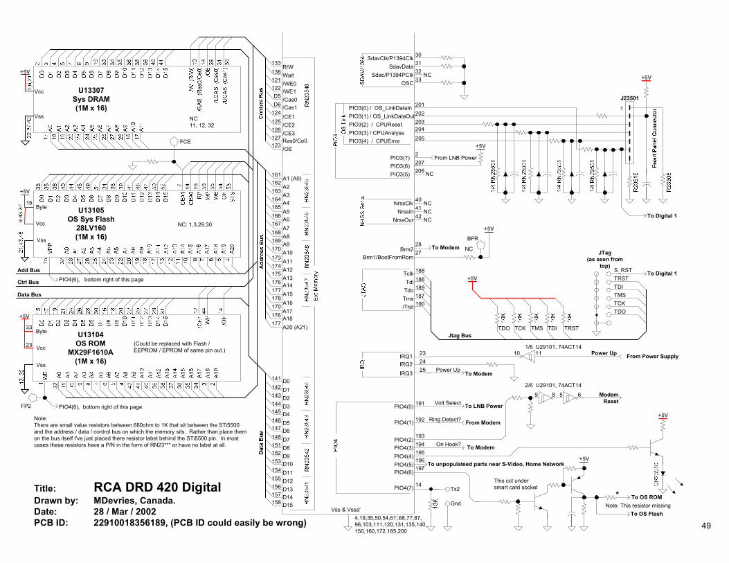
+5V
Jtag Bus
201202203204
PIO3(0) / OS_LinkDataIn
205PIO3(4) / CPUErrorPIO3(3) / CPUAnalysePIO3(2) / CPUResetPIO3(1) / OS_LinkDataOut
PIO3(5)PIO3(6)PIO3(7)
2062072
NC
Vcc
Byte
+5V
33
23
Vss
U13104OS ROM
MX29F1610A(1M x 16)
Title: RCA DRD 420 DigitalDrawn by: MDevries, Canada.Date: 28 / Mar / 2002PCB ID: 22910018356189, (PCB ID could easily be wrong)
Data Bus
Ctrl Bus
Add Bus
4,19,35,50,54,61',68,77,87,96,103,111,120,131,135,140,150,160,172,185,200
Vss & Vssa'
NC
NCNC
40
4241
NrssClk
NrssOurNrssIn
Brm1/BootFromRom27Brm228
NC
30
333231
SdavClk/P1394Clk
OSCSdac/P1394PClk
SdavData
TclkTdi
TdoTms/Trst
188186189187190
Vcc
Byte
+5V
U13105OS Sys Flash
28LV160(1M x 16)
15
Vss
NC: 1,3,29,30
+5V
NC11, 12, 32
U13307Sys DRAM(1M x 16)
Vcc
Vss
141142143144145146147148151152153154155156157158
D0D1D2D3D4D5D6D7D8D9D10D11D12D13D14D15
R/WWait/WE0/WE1/Cas0/Cas1/CE1/CE2/CE3Ras0/Ce0/OE
133136121122D5D6
124125126127123
A1 (A0)A2A3A4A5A6A7A8
A10A11
A9
A12A13
161162163164165166167168169170173174175
A15A16
A14
A17
176177178170
A20 (A21)A18176
177
191
192
193194
PIO4(0)
195PIO4(4)PIO4(3)PIO4(2)
PIO4(1)
PIO4(5)196
PIO4(6)197
PIO4(7) 14
FCE
From LNB Power
J23501
1
+5V
23IRQ1IRQ2IRQ3
2425
11101/6 U29101, 74ACT14
Power Up From Power Supply
+5V
2/6 U29101, 74ACT14Modem
Reset9 8 5 6
Power UpTo Modem
To LNB Power
From ModemRing Detect?
To ModemOn Hook?
NC
BFR
+5V
To Modem
+5V
This cct undersmart card socketTx2
Gnd
To OS Flash
* To OS ROMNote: This resistor missing
PIO4(6), bottom right of this page
PIO4(6), bottom right of this page
(Could be replaced with Flash /EEPROM / EPROM of same pin out.)
Note:There are small value resistors between 680ohm to 1K that sit between the STi5500and the address / data / control bus on which the memory sits. Rather than place themon the bus itself I've just placed there resistor label behind the STi5500 pin. In mostcases these resistors have a P/N in the form of RN23*** or have no label at all.
To unpopulateed parts near S-Video, Home Network
+5V
TRSTTDITMSTCKTDO
JTag(as seen from
top)
TDOTCKTMSTDITRSTS_RST To Digital 1
To Digital 1
FP2 Volt Select
49
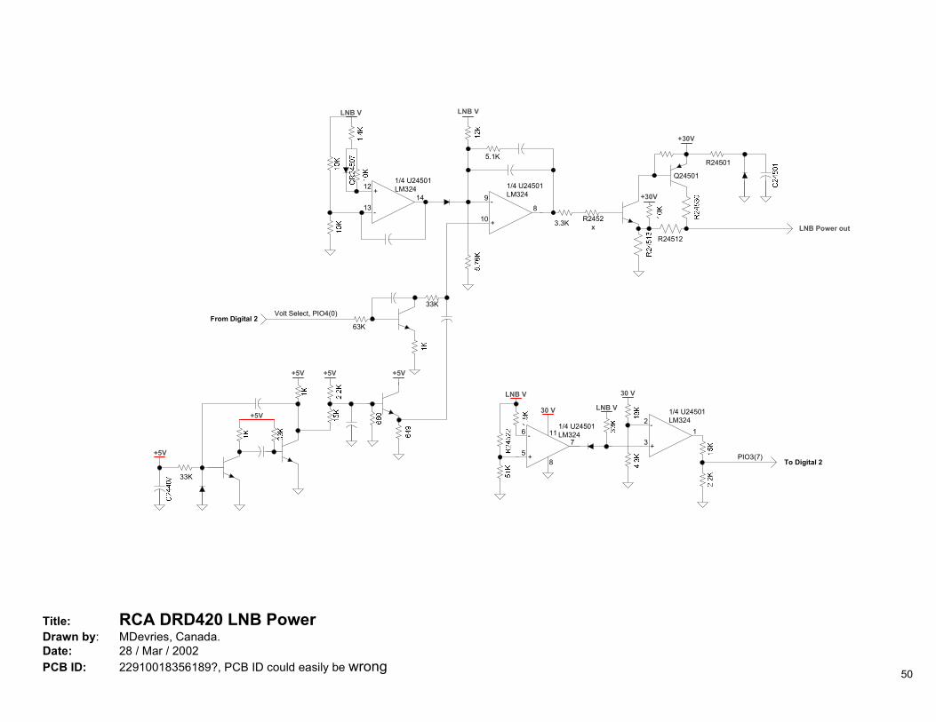
Title: RCA DRD420 LNB PowerDrawn by: MDevries, Canada.Date: 28 / Mar / 2002PCB ID: 22910018356189?, PCB ID could easily be wrong
From Digital 263K
33KVolt Select, PIO4(0)
+5V
+5V
+5V +5V +5V
LNB Power out
+30V
Q24501
R24512
810
9 -
+ R2452x
1/4 U24501LM324
LNB V
5.1K
3.3K
+30V1412
13 -
+
LNB V
1/4 U24501LM324
R24501
33K
75
6 -
+
LNB V
LNB V
13
2 -
+
30 V
1/4 U24501LM324
1/4 U24501LM324
To Digital 2PIO3(7)
8
30 V
11
50
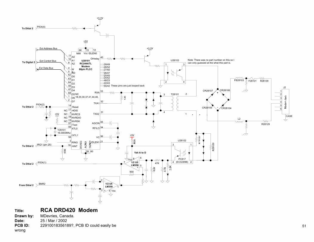
Title: RCA DRD420 ModemDrawn by: MDevries, Canada.Date: 25 / Mar / 2002PCB ID: 22910018356189?, PCB ID could easily bewrong
8Vcc
1bit A to D
6
5+
-7 1/2 U5
LM358
900
+5V
47K
15
RING
U28101RC244ATL
Modem68pin PLCC
RD
14
NC18,20,30,37,41,44,46,
IDLEN1
RXA
+5V
VccNMI
VC
21
IDLEN066
Reset
Y2810116.0003Mhz
/Test57
+5V
RFILO
AGCIN
36
34
39 60
NVRDIONVRSK
NVRCS1913
7
XTL0
/XTL1
59
58
To Digital 2
16 HINTTo Ditial 2 IRQ1 (pin 25)
NCNCNC
HDIS
Ext Contorl Bus
Ext Data Bus WT
62636465676812
45
108
11 A0A1A2
D0D1D2D3D4D5D6D7
Ext Address Bus
To Ditial 217NC
29/4928/5227/5026/4725/45
OHrelay 40
24/5248/2322/4355/42
T28101
1
2
3
TXA1
TXA2
33
32
31
12
These pins are just looped back
35
4
3
PC817(ECG3098)
U28102
4
3
2
1
U28103
4
3
2
1
+3.3V
+3.3V
To Ditial 2
FB28103
L2
R28129
4321
56
CASE
J2
R28129F28101
CR28104CR28105
CR28106CR28107+
-
Note: There was no part number on this so Ican only guessed at the what this part is.
143
2
Vss+
-1/2 U5LM358
To Ditial 2
From Ditial 2
PIO4(2)
PIO4(1)
PIO4(4)
BMR2
51
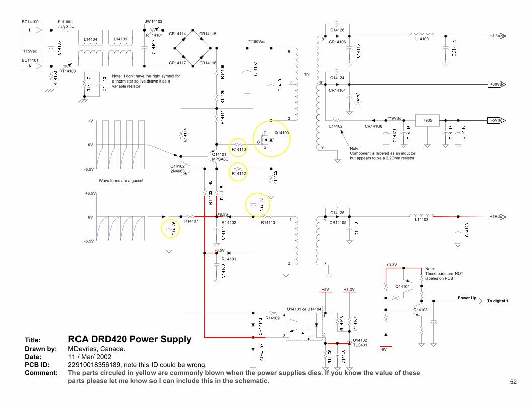
Title: RCA DRD420 Power SupplyDrawn by: MDevries, Canada.Date: 11 / Mar/ 2002PCB ID: 22910018356189, note this ID could be wrong.Comment: The parts circuled in yellow are commonly blown when the power supplies dies. If you know the value of these
parts please let me know so I can include this in the schematic.
5
3
D
GS
6+5Vdc
L14103CR14105
7
C14125
Q14100
T01
CR14114 CR14115
CR14117 CR14116
RT14101L14101L14104
F14100/1?.?A Slow
L
N
115Vac
RT14100
BC14100
BC14101
JW14103
Note: I don't have the right symbol fora thermister so I've drawn it as avariable resistor
+3.3VdcL141008
CR14106
C14126
+30Vdc10
CR14104
C14124
9
CR14108-5Vdc7905~9Vdc
~150Vac
2
L14102
Note:Component is labeled as an inductor,but appears to be a 2.2Ohm resistor
R14112
R14110Q14101MPSA86
2
R141131R14107 R14102
+6.5V
1
2
U14101 or U14104
3
4
+5V +3.3V
U14102TLC431
R14109
R14101
-6.5V
Q141022N4063
Q14103
Q14104
Note:These parts are NOTlabeled on PCB
+3.3V
-9V
To digital 1Power Up
-6.5V
0V
+6.5V
-6.5V
0V
+V
Wave forms are a guess!
52
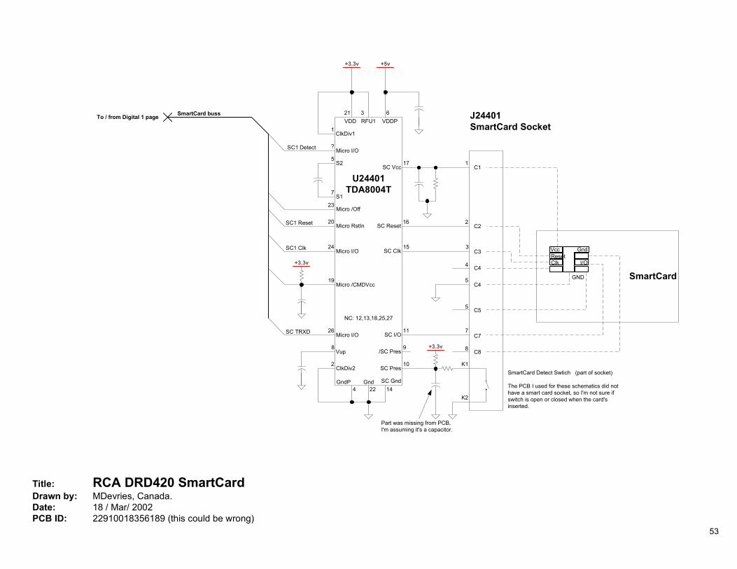
Title: RCA DRD420 SmartCardDrawn by: MDevries, Canada.Date: 18 / Mar/ 2002PCB ID: 22910018356189 (this could be wrong)
J24401SmartCard Socket
K2
3
5
K1
SmartCard
SmartCard Detect Swtich (part of socket)
The PCB I used for these schematics did nothave a smart card socket, so I'm not sure ifswitch is open or closed when the card'sinserted.
GND
GndVcc
I/OResetClk
SC1 Detect
SmartCard bussTo / from Digital 1 page
C7
C5
C3
C2
C1
2
17
16
15
11
SC Vcc
SC Reset
SC Clk
U24401TDA8004T
1
7
+5v+3.3v
621 3
1ClkDiv1
RFU1VDD VDDP
ClkDiv2
+3.3v
10
14
2
?
Part was missing from PCB,I'm assuming it's a capacitor.
S2
S1
5
7
SC1 Clk 24
SC TRXD
SC1 Reset 20Micro RstIn
NC: 12,13,18,25,27
SC I/O
SC Pres
SC GndGndP
Micro I/O
C44
C4
5
C88
4 22Gnd
8Vup
+3.3v
19
26
9/SC Pres
Micro /CMDVcc
Micro I/O
Micro I/O
23Micro /Off
53
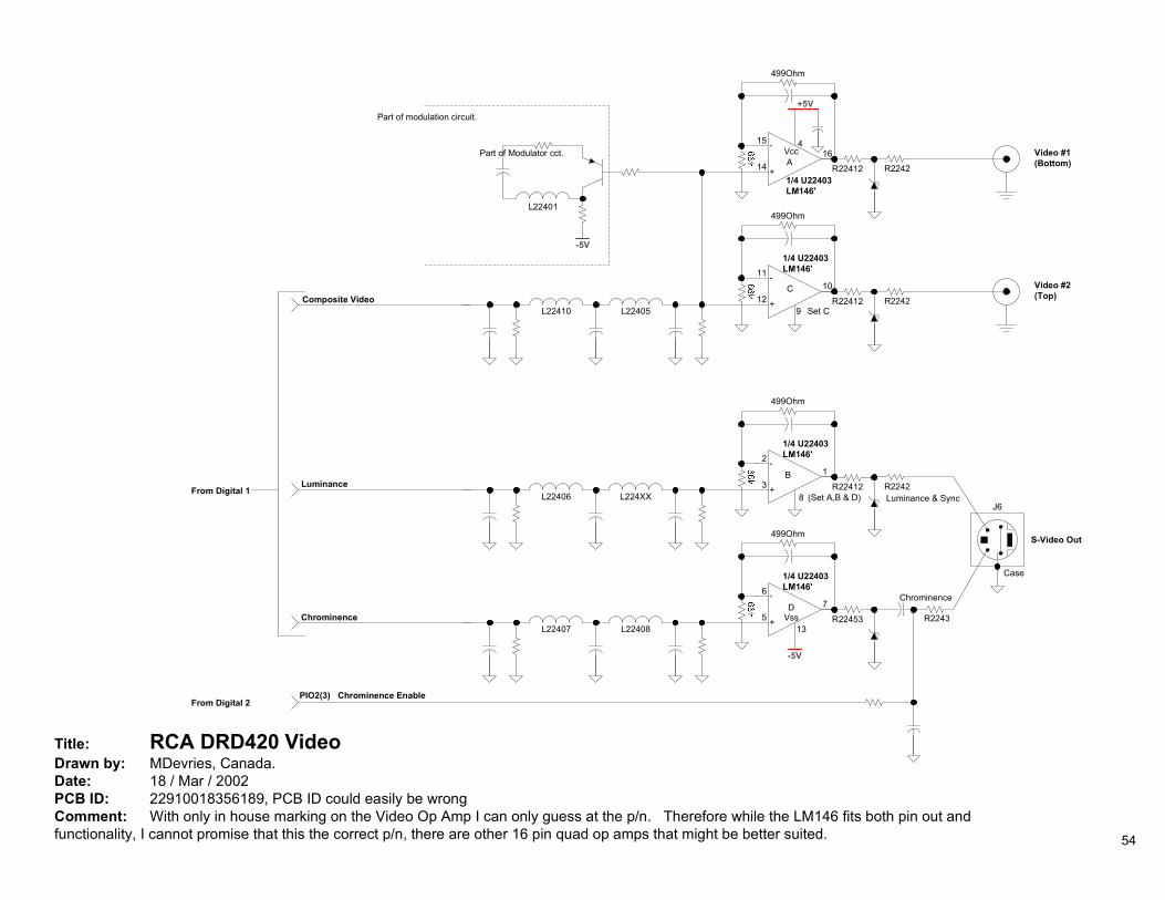
Title: RCA DRD420 VideoDrawn by: MDevries, Canada.Date: 18 / Mar / 2002PCB ID: 22910018356189, PCB ID could easily be wrongComment: With only in house marking on the Video Op Amp I can only guess at the p/n. Therefore while the LM146 fits both pin out andfunctionality, I cannot promise that this the correct p/n, there are other 16 pin quad op amps that might be better suited.
From Digital 1
Composite Video
Chrominence
J6
Case
S-Video Out
R22453
499Ohm
75
6 -
+
1/4 U22403LM146'
R2243
-5V
VssD
L22408L22407Chrominence
PIO2(3) Chrominence EnableFrom Digital 2
L22401
-5V
Video #1(Bottom)R22412
499Ohm
1614
15 -
+1/4 U22403LM146'
R2242
Vcc
+5V
4
A
Video #2(Top)R22412
499Ohm
1012
11 -
+
1/4 U22403LM146'
R22429 Set C
C
L22405L22410
Luminance & SyncR22412
499Ohm
13
2 -
+
1/4 U22403LM146'
R2242B
8 (Set A,B & D)L224XXL22406Luminance
13
Part of Modulator cct.
Part of modulation circuit.
54
Related Documents