FUJITSU. 68, 1, p. 43-50 (01, 2017) 43 あらまし 炭素原子が蜂の巣状に結びついた原子一層分の材料であるグラフェンおよびそれを丸 めて円筒状の構造にしたカーボンナノチューブは,高い電子移動度,高い電流密度耐性 などの優れた電気特性のほか,高い熱伝導性・機械的強度を持ち,将来の電子デバイス 用の材料として期待されている。シリコントランジスタに代表される半導体デバイスの 微細化限界が目前に迫った今,筆者らのグループでは将来のブレークスルーを目指し, ナノカーボン材料のエレクトロニクス応用を目指した研究を行っている。 本稿では,まずナノカーボン材料の電子状態や特性,またその特性から期待されてい る応用について概説する。次いで,筆者らが取り組んできたナノカーボン材料の合成技 術のほか,トランジスタ,配線,および放熱への応用を目指したこれまでの取り組みに ついて説明する。更には,現在取り組みつつある究極のデバイスを目指したグラフェン ナノリボンの合成技術についても簡単に述べる。 Abstract Graphene, a one-atom-thick honeycomb lattice made of carbon, and a carbon nanotube, a rolled-up graphene sheet, have excellent electrical properties, such as high electron mobility and tolerance to a high current density. They also have high thermal conductivity and mechanical strength, and are therefore promising materials for future electronic devices. Facing the limit of scaling (miniaturization) of semiconductor devices represented by silicon transistors, our group is researching ways to apply nanocarbon materials (graphene and carbon nanotubes) to electronics for a breakthrough. In this article, we first explain the electronic states and properties of nanocarbon materials, as well as expectations for applying them that come from their excellent properties. We then describe the method of growing nanocarbon materials, followed by an explanation of our efforts to apply such materials to transistors, interconnects, and thermal interface material (TIM). Finally, we briefly explain a technology to synthesize a graphene nanoribbon, a narrow strip of graphene, which we are working on in order to develop devices with superb properties. ● 佐藤信太郎 ● 近藤大雄 ● 廣瀬真一 ● 山口淳一 革新的デバイス創製に向けた ナノカーボン材料技術 Nanocarbon Technology for Development of Innovative Devices

Welcome message from author
This document is posted to help you gain knowledge. Please leave a comment to let me know what you think about it! Share it to your friends and learn new things together.
Transcript
FUJITSU. 68, 1, p. 43-50 (01, 2017) 43
あ ら ま し
炭素原子が蜂の巣状に結びついた原子一層分の材料であるグラフェンおよびそれを丸
めて円筒状の構造にしたカーボンナノチューブは,高い電子移動度,高い電流密度耐性
などの優れた電気特性のほか,高い熱伝導性・機械的強度を持ち,将来の電子デバイス
用の材料として期待されている。シリコントランジスタに代表される半導体デバイスの
微細化限界が目前に迫った今,筆者らのグループでは将来のブレークスルーを目指し,
ナノカーボン材料のエレクトロニクス応用を目指した研究を行っている。
本稿では,まずナノカーボン材料の電子状態や特性,またその特性から期待されてい
る応用について概説する。次いで,筆者らが取り組んできたナノカーボン材料の合成技
術のほか,トランジスタ,配線,および放熱への応用を目指したこれまでの取り組みに
ついて説明する。更には,現在取り組みつつある究極のデバイスを目指したグラフェン
ナノリボンの合成技術についても簡単に述べる。
Abstract
Graphene, a one-atom-thick honeycomb lattice made of carbon, and a carbon nanotube, a rolled-up graphene sheet, have excellent electrical properties, such as high electron mobility and tolerance to a high current density. They also have high thermal conductivity and mechanical strength, and are therefore promising materials for future electronic devices. Facing the limit of scaling (miniaturization) of semiconductor devices represented by silicon transistors, our group is researching ways to apply nanocarbon materials (graphene and carbon nanotubes) to electronics for a breakthrough. In this article, we first explain the electronic states and properties of nanocarbon materials, as well as expectations for applying them that come from their excellent properties. We then describe the method of growing nanocarbon materials, followed by an explanation of our efforts to apply such materials to transistors, interconnects, and thermal interface material (TIM). Finally, we briefly explain a technology to synthesize a graphene nanoribbon, a narrow strip of graphene, which we are working on in order to develop devices with superb properties.
● 佐藤信太郎 ● 近藤大雄 ● 廣瀬真一 ● 山口淳一
革新的デバイス創製に向けたナノカーボン材料技術
Nanocarbon Technology for Development of Innovative Devices
FUJITSU. 68, 1 (01, 2017)44
革新的デバイス創製に向けたナノカーボン材料技術
されるナノカーボン材料が非常に有力な候補であると考えている。もちろん,ナノカーボン材料の採用によって必ずしも微細化が進むわけではなく,ナノカーボン材料が現在電子デバイスの抱える全ての問題を解決できるわけでもない。しかし,その高い電子移動度や電流密度耐性,特異な電子状態から導かれるクライントンネリングなどの不思議な物性は,現在のデバイスの限界を打破する大きな可能性を感じさせる。また高周波デバイスや,各種センサーなどのいわゆるMore than Mooreデバイスに向けた材料としても有望である。本稿では,ナノカーボン材料であるグラフェンやCNTの電子状態や特性,そこから期待される応用などについて概説した後,トランジスタ,配線,および放熱への応用を目指したこれまでの取り組みを述べる。更には,現在取り組みつつある,究極のデバイスを目指したグラフェンナノリボン(GNR)合成技術についても説明する。
グラフェンとCNT
グラフェンは層状材料であるグラファイトの一層分のシートであり,図-1(a)に示すように,炭素原子が蜂の巣状に結びついた平面構造を有して
グラフェンとCNT
ま え が き
シリコン大規模集積回路(LSI)は,これまで微細化によってその性能(速度,消費電力)を向上させるとともに,トランジスタ1個あたりのコストを低減してきた。しかし,微細化による性能向上は鈍化しており,2020年以降にチャネル長が10 nmを切る頃には,いよいよ微細化の限界が訪れるものと予想されている。しかし,電子デバイスの高性能化への希求は今後も止むことがないであろうし,今話題の人工知能(AI:Artifi cial Intelligence)が本当の意味で現実になるためには,今より遥かに高い計算能力が必要であるとも言われている。個々のデバイスエレメントの性能だけで計算能力が決まるものではないとしても,我々は今,微細化に代わる新たなデバイス高性能化の道筋を考えなければならない状況にある。デバイス高性能化の道筋として,3次元集積をはじめ様々な提案がなされている。その一つの選択肢として挙げられるのが,新たな材料の採用によるトランジスタなどのデバイスエレメントの性能向上である。筆者らはそのような材料として,グラフェンやカーボンナノチューブ(CNT)に代表
ま え が き
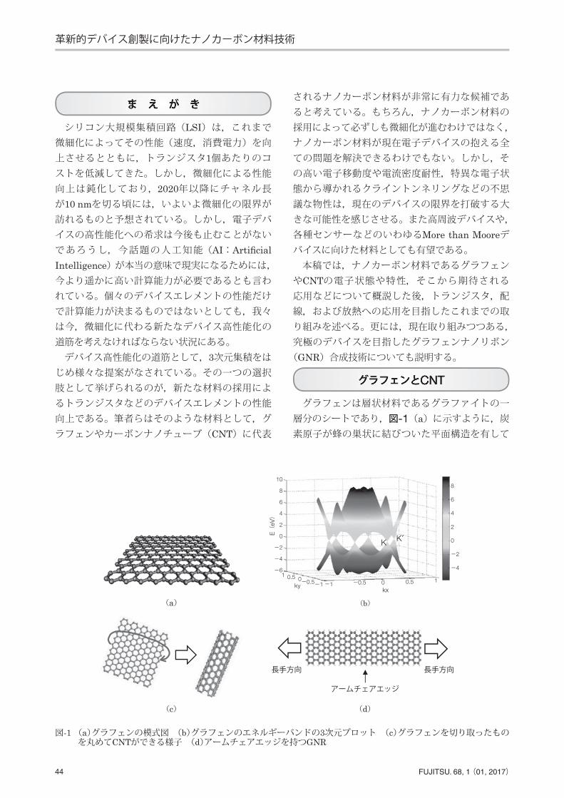
図-1 (a)グラフェンの模式図 (b)グラフェンのエネルギーバンドの3次元プロット (c)グラフェンを切り取ったものを丸めてCNTができる様子 (d)アームチェアエッジを持つGNR
K’K
(a) (b)
(c) (d)
アームチェアエッジ
長手方向長手方向
10
8
6
4
2
0
-2
-4
-6
8
6
4
2
0
-2
-4
E(
eV)
kykx
1 0.5 0-0.5 -0.5 0 0.5 1-1-1
FUJITSU. 68, 1 (01, 2017) 45
革新的デバイス創製に向けたナノカーボン材料技術
いる。その単位格子は,非等価な炭素2原子からなる。この構造から,図-1(b)に模式的に示すように,波数空間の2点(K点およびK’点)付近でエネルギーが波数に対して線形の分散関係を持つという特異な電子状態となる。線形であるということは,エネルギーを波数で偏微分して得られる速度が一定であることを示し,実際グラフェン中の電子は,質量ゼロのニュートリノと同様の方程式に従う(速度は光の1/300)。詳細は省くが,このような電子状態から,グラフェン中の電子は後方散乱の消失や,クライントンネリング,半整数量子ホール効果などの特異な性質を示す。(1)このうち後方散乱の消失は,グラフェンの長いバリスティック長(電子が散乱されることなく移動できる距離)およびそれからもたらされる高い電子移動度(液体ヘリウム温度で106 cm2/Vs程度)を担保することになる。ただしグラフェンには,図-1(b)から分かるようにバンドギャップ(電子状態における,価電子帯頂上と伝導帯底のエネルギー差)がなく,そのままでは通常のトランジスタのチャネルとして使用することは難しい。
CNTはグラフェンを丸めて円筒状にしたものであるため{図-1(c)},その電子状態はグラフェンと類似の手法で求められる。ただし,その丸め方(カイライリティ)によって,1/3が金属,2/3が半導体となる。また半導体の場合でも,CNTの直径が大きいほどバンドギャップは小さくなる。このような電子状態の変化は,グラフェンを短冊状にしたGNRでも同様である。特に,図-1(d)に示すようなアームチェア型のエッジを持つものは全てバンドギャップを有しており,半導体的性質を備えることになる。グラフェンやCNTは,高い電子移動度と高い電流密度耐性(銅の1,000倍程度)を有するため,トランジスタのチャネル材料のほか,配線材料としても有望視されている。更に,高い熱伝導率(銅の約10倍)や機械的強度を有しているため,放熱材料や樹脂などの補強材料としても期待されており,既に実用化もされている。次章以降では,こうしたナノカーボン材料の合成,応用についての筆者らの取り組みを紹介する。
ナノカーボン材料の合成
グラフェンやCNTは,化学気相合成法(CVD:Chemical Vapor Deposition)により,シリコンなどの基板上に合成できる。基本的には,基板上に鉄,ニッケル,コバルトに代表される遷移金属の薄膜を触媒として堆積させ,500~ 1,000℃程度の高温下でメタン,アセチレンなどの炭化水素系ガスを用いてCVDを行うことにより合成できる。触媒金属膜が数nm程度と薄い場合,基板を熱した際に触媒金属が微粒子化し,それをシード(種)としてCNTが合成される。一方,条件にもよるが触媒層の膜厚が数十nm以上と厚い場合には,グラフェンが形成される。(2)鉄,ニッケル,コバルトなどを触媒として使用すると,一般的に多層のグラフェン(グラファイト)が形成されるが,銅を触媒とした場合には,単層のグラフェンが選択的に形成できる。
トランジスタへの応用
グラフェンやCNTは電子移動度が高いため,トランジスタのチャネル材料として期待されている。実際,GNRあるいはCNTを多数並べて作製したトランジスタの特性は,シリコンナノワイヤなどによるものに比べて高い電流駆動能力を持つことがシミュレーションにより予想されている。(3)
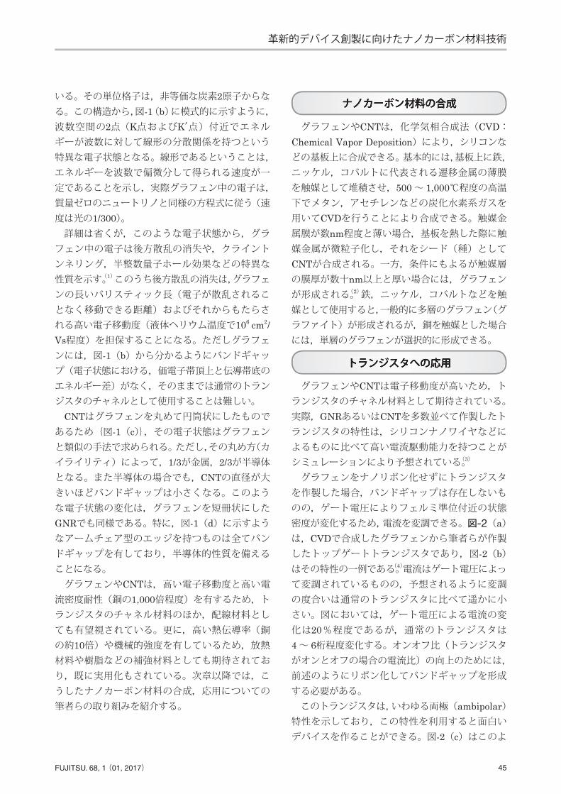
グラフェンをナノリボン化せずにトランジスタを作製した場合,バンドギャップは存在しないものの,ゲート電圧によりフェルミ準位付近の状態密度が変化するため,電流を変調できる。図-2(a)は,CVDで合成したグラフェンから筆者らが作製したトップゲートトランジスタであり,図-2(b)はその特性の一例である。(4)電流はゲート電圧によって変調されているものの,予想されるように変調の度合いは通常のトランジスタに比べて遥かに小さい。図においては,ゲート電圧による電流の変化は20%程度であるが,通常のトランジスタは4~ 6桁程度変化する。オンオフ比(トランジスタがオンとオフの場合の電流比)の向上のためには,前述のようにリボン化してバンドギャップを形成する必要がある。このトランジスタは,いわゆる両極(ambipolar)特性を示しており,この特性を利用すると面白いデバイスを作ることができる。図-2(c)はこのよ
ナノカーボン材料の合成
トランジスタへの応用
FUJITSU. 68, 1 (01, 2017)46
革新的デバイス創製に向けたナノカーボン材料技術
うなグラフェンを用いたデュアルゲートトランジスタの模式図である。バックゲートに正あるいは負の電位Vbgを与えることにより,トップゲート電圧Vtgに対する応答Idを図-2(d)のようにシフトさせることができる。この特性を利用して,例えば図-2(e)のような回路を組むと,バックゲートを入力とした二位相偏移変調器を作製できる。(5)この変調法は,無線LANで使われているデジタル変調の一種である。この場合,バックゲートの電圧Vdataの正負(HあるいはL)に応じて,トップゲートからの入力Vsin
に対する応答Voutが反転するため,信号の位相が
180度変化する。このように,グラフェントランジスタの特性をうまく利用することにより,これまでとは一味違う新しいデバイスの作製が可能となる。
配線への応用
グラフェンやCNTは,長いバリスティック長および高い電流密度耐性から,LSIなどの微細配線用材料として期待されている。筆者らは,これらのLSI配線への応用に10年ほど前から取り組んできた。半導体の配線工程では低いプロセス温度が要求されるため,グラフェンやCNTを400℃程度の温
配線への応用
図-2 (a)CVDで合成したグラフェンをチャネルとしたトップゲートトランジスタの模式図と光学顕微鏡写真。グラフェンチャネルの幅(W)は3 µm,長さ(L)は2 µm,ゲート絶縁膜厚(t)は70 nm,ドレイン電圧(Vd)は1.4 V (b)(a)に示したトップゲートトランジスタの特性の一例 (c)デュアルゲートトランジスタの模式図 (d)バックゲート電圧(Vbg)によりトップゲート電圧(Vtg)に対する応答がシフトし,極性が異なるトランジスタとして動作することを示す例 (e)(c)のデュアルゲートトランジスタに抵抗を組み合わせて作製した二位相偏移変調器。バックゲート電圧の正負がVdataのH,Lに対応。トップゲートに入力されたサイン波に対し,VdataがHのときに位相が反転してVoutに出力される
VtgVtg
I d(m
A)
Vtg(V)
Vbg<0 Vbg>0
Vbg=5 V
0 V
-5 V-10 V-15 V
0.5
0.4
0.3
0.2-3 -2 -1 0 1 2 3
ゲート電圧(V)
ドレイン電流(
mA)
L = 2 µm
W = 3 µm
t = 70 nm
Vd = 1.4 V
(a) (b) (c)
(d)
1.75
1.70
1.65
1.60
1.55
1.50
1.45-15 -10 -5 0 5 10 15
Ti/Auソース
Ti/Auバックゲート
p+-Si基板
AI2O3絶縁膜
SiO2絶縁膜(100 nm)
Ti/Auトップゲート
グラフェンチャネル
Ti/Auドレイン
VtgVtg
I d(m
A)
Vtg(V)
Vbg<0 Vbg>0
Vbg=5 V
0 V-5 V-10 V-15 V
0.5
0.4
0.3
0.2-3 -2 -1 0 1 2 3
グラフェン
ソース ドレイン
トップゲート
基板
ソース
ドレイン
トップゲート
グラフェン
Vsupply
Vsin
Vout
Vdata
Vsupply
Vsin
Vout
Vdata
Vsupply
Vsin
Vout
Vdata
(e)
Vsin
Vout
Vdata=‘H’
Vdata=‘L’
搬送波
FUJITSU. 68, 1 (01, 2017) 47
革新的デバイス創製に向けたナノカーボン材料技術
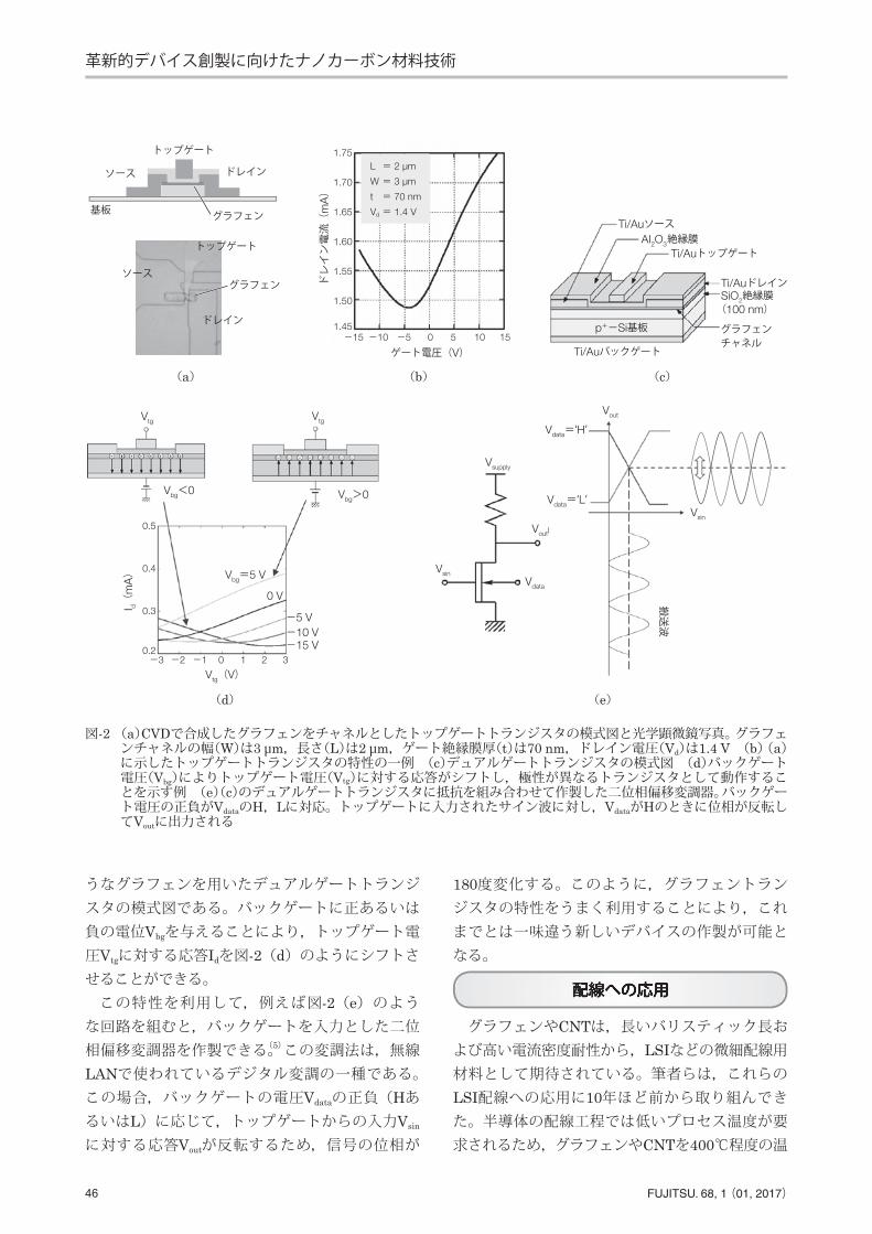
度で合成する必要がある。筆者らは実際,このような低い温度でのCNTの合成に成功している。しかし,それがグラフェンであれCNTであれ,こうした低温で合成したものは電気特性(抵抗)として十分なものは得られていない。そこで,グラフェンおよびCNTを高温条件のもとで品質の高いものを別の基板上に形成し,それを配線用基板に転写して配線を形成するという方法を採用した。(6),(7)
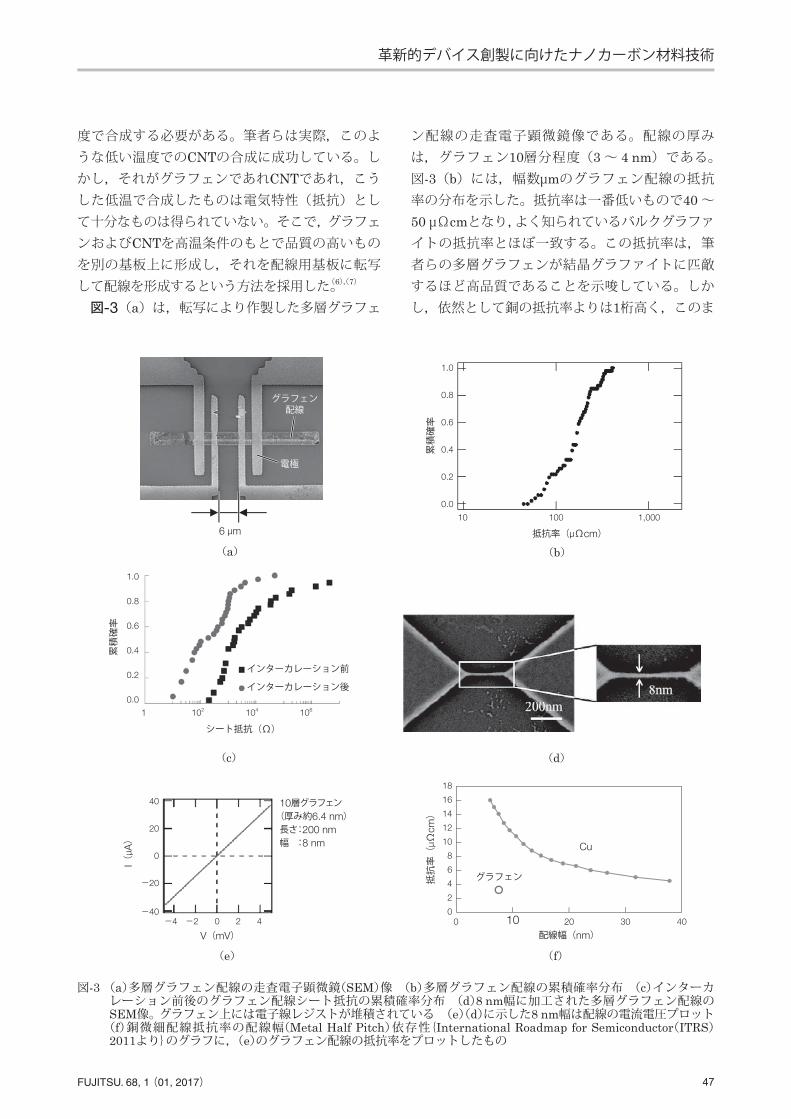
図-3(a)は,転写により作製した多層グラフェ
ン配線の走査電子顕微鏡像である。配線の厚みは,グラフェン10層分程度(3~ 4 nm)である。図-3(b)には,幅数µmのグラフェン配線の抵抗率の分布を示した。抵抗率は一番低いもので40~50 µΩcmとなり,よく知られているバルクグラファイトの抵抗率とほぼ一致する。この抵抗率は,筆者らの多層グラフェンが結晶グラファイトに匹敵するほど高品質であることを示唆している。しかし,依然として銅の抵抗率よりは1桁高く,このま
図-3 (a)多層グラフェン配線の走査電子顕微鏡(SEM)像 (b)多層グラフェン配線の累積確率分布 (c)インターカレーション前後のグラフェン配線シート抵抗の累積確率分布 (d)8 nm幅に加工された多層グラフェン配線のSEM像。グラフェン上には電子線レジストが堆積されている (e)(d)に示した8 nm幅は配線の電流電圧プロット(f)銅微細配線抵抗率の配線幅(Metal Half Pitch)依存性{International Roadmap for Semiconductor(ITRS)2011より}のグラフに,(e)のグラフェン配線の抵抗率をプロットしたもの
40
20
0
-20
-4 -2 0 2 4-40
I(µ A)
V(mV)
(a)
グラフェン配線
電極
6 µm
(c) (d)
(e)
10層グラフェン(厚み約6.4 nm)長さ :200 nm幅 :8 nm
0
2
4
6
8
10
12
14
16
18
0 10 20 30 40
配線幅(nm)
Cu
グラフェン
(f)
抵抗率(
µΩcm)
累積確率
シート抵抗(Ω)
インターカレーション前
インターカレーション後
1.0
0.8
0.6
0.4
0.2
0.0
1 102 104 106
1.0
0.8
0.6
0.4
0.2
0.0
10 100 1,000
(b)抵抗率(µΩcm)
累積確率
FUJITSU. 68, 1 (01, 2017)48
革新的デバイス創製に向けたナノカーボン材料技術
までは銅配線を置き換えることは難しい。更なる低抵抗化を図るため,筆者らは多層グラフェンの層間に異種分子を挿入(インターカレーション)することによる伝導キャリア濃度の増加を試みた。インターカレーション前後のシート抵抗分布を図-3(c)に示す。抵抗はインターカレーション後,中央値で約20分の1に低下した。厚みから抵抗率を見積もると,最も良い抵抗率は1.5 µΩcmと銅を凌駕するものが得られることが分かった。上記の結果は幅6 µmの配線に関するものであったが,筆者らは更に電子ビームリソグラフィを用いて,幅10 nm以下の微細配線を形成した。幅8 nmの多層グラフェン配線の走査電子顕微鏡像を図-3(d)に示す。図-3(e)はこの微細配線の電流電圧特性を示す。電流値は電圧に対して線形であり,リソグラフィで加工したGNRでよく見られる伝導率の大幅な低下は見られていない。この配線の抵抗率は3.2 µΩcmであり,図-3(f)に示す銅
の微細配線の予測値(ITRS2011より)より良好なことが分かる。(7)もちろんこれはベストの値であり,インターカレーションプロセスなどに起因したばらつきを減らすことが今後必要となる。しかし本結果は,グラフェン微細配線が銅配線より優れた抵抗率を持ち得ることを示す初めての結果であり,グラフェンの微細配線材料としての可能性を示すものである。
放熱への応用
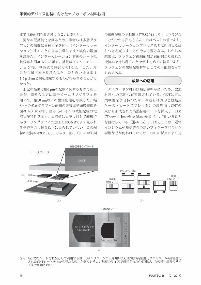
ナノカーボン材料は熱伝導率が高いため,放熱材料への応用も有望視されている。CNTは更に柔軟性を併せ持つため,筆者らはCPUと放熱用ケース(ヒートスプレッダ)の境界面にCNTの束から形成された高熱伝導シートを挿入し,TIM(Thermal Interface Material)として用いることを目指している{図-4(a)}。TIMとしては,通常インジウムや熱伝導性の高いフィラーを混合した樹脂などが使われているが,CNTの採用により更
放熱への応用
図-4 (a)CNTシートをTIMとして利用する例 (b)シリコーンゴムを用いたCNT束の高密度化プロセス (c)高密度化されたCNTシートを上から見たもの。左側のシリコン基板のサイズで成長されたCNT束が,右の黒い部分のサイズまで圧縮された
(a) (b)
CNT-TIM
CPU
高熱伝導率CNTシート
ヒートスプレッダ
CNT層
(c)
3インチ Si ウェハ(CNT除去後)
圧縮CNTシート
シリコーンゴム
圧縮CNTシート成長後
CNTシート
シリコーンゴム
FUJITSU. 68, 1 (01, 2017) 49
革新的デバイス創製に向けたナノカーボン材料技術
に熱抵抗が下がることが期待されている。CNT束をTIMとして使用する場合,熱抵抗を下げるためにCNTの単位面積あたりの本数(密度)を高めることが重要である。そこで筆者らは,CNTの合成条件を最適化するだけではなく,CNT膜の転写法に工夫を施した。図-4(b)に示すように,水平方向に引き伸ばしたシリコーンゴムにCNTを転写し,その後ゴムを元に戻すことにより,CNTの密度を3倍程度向上させた。(8)作製されたCNTシートの高さは約140 µm,CNTの空間占有率は8~ 9%程度である。このように作製されたシートを二つの銅ブロック(一つは熱源に接続され,一つはヒートシンクとして冷却されている)で挟んだときの銅ブロック間の温度差は1.06℃であり,インジウム製のTIMと同程度であった。CNT-TIMはインジウムでは対応不可能な,高さの異なるマルチチップにも対応できる。また,通常マルチチップに使用される熱伝導性の高いフィラーを混合した樹脂製TIMよりも熱抵抗が低いため,今後CNT-TIMの実用化が期待される。
GNRのボトムアップ合成
トランジスタへの応用の章でも述べたように,グラフェンにはバンドギャップがなく,バンドギャップを形成するためには,幅が狭いリボン状にする必要がある。ただし,必要とされる幅は数nm以下と極めて狭い。筆者らはこれまで,配線への応用の章で触れた電子ビームリソグラフィや,ヘリウムイオンビームを用いた直接エッチング(9)
などでGNR形成を試みてきたが,トランジスタ特
GNRのボトムアップ合成
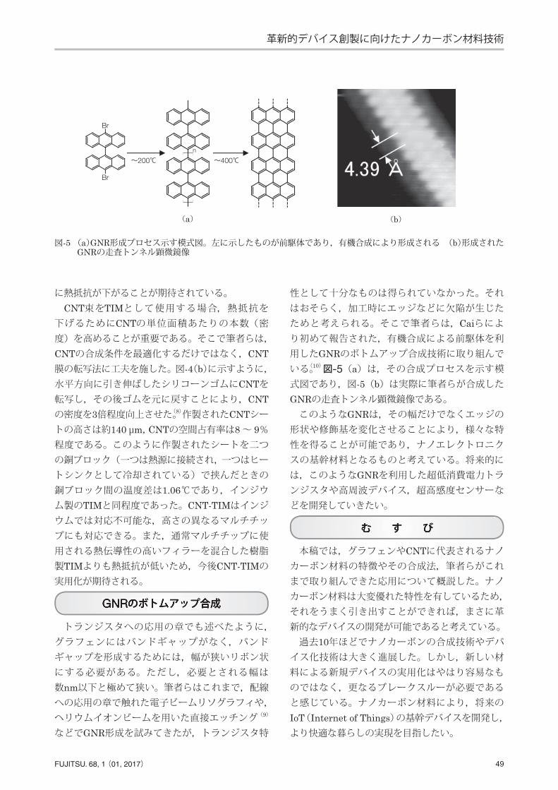
性として十分なものは得られていなかった。それはおそらく,加工時にエッジなどに欠陥が生じたためと考えられる。そこで筆者らは,Caiらにより初めて報告された,有機合成による前駆体を利用したGNRのボトムアップ合成技術に取り組んでいる。(10)図-5(a)は,その合成プロセスを示す模式図であり,図-5(b)は実際に筆者らが合成したGNRの走査トンネル顕微鏡像である。このようなGNRは,その幅だけでなくエッジの形状や修飾基を変化させることにより,様々な特性を得ることが可能であり,ナノエレクトロニクスの基幹材料となるものと考えている。将来的には,このようなGNRを利用した超低消費電力トランジスタや高周波デバイス,超高感度センサーなどを開発していきたい。
む す び
本稿では,グラフェンやCNTに代表されるナノカーボン材料の特徴やその合成法,筆者らがこれまで取り組んできた応用について概説した。ナノカーボン材料は大変優れた特性を有しているため,それをうまく引き出すことができれば,まさに革新的なデバイスの開発が可能であると考えている。過去10年ほどでナノカーボンの合成技術やデバイス化技術は大きく進展した。しかし,新しい材料による新規デバイスの実用化はやはり容易なものではなく,更なるブレークスルーが必要であると感じている。ナノカーボン材料により,将来のIoT(Internet of Things)の基幹デバイスを開発し,より快適な暮らしの実現を目指したい。
む す び
図-5 (a)GNR形成プロセス示す模式図。左に示したものが前駆体であり,有機合成により形成される (b)形成されたGNRの走査トンネル顕微鏡像
(a) (b)
Br
Br
n
~200℃ ~400℃
FUJITSU. 68, 1 (01, 2017)50
革新的デバイス創製に向けたナノカーボン材料技術
本研究の一部は,産業技術総合研究所において,内閣府/日本学術振興会・最先端研究開発支援プログラムの支援を受けて行ったものです。また本研究の一部は,JST CRESTの支援を受けています。
参 考 文 献
(1) A. H. Castro. Neto et al.:The Electronic Properties of Graphene.Rev. Mod. Phys.,Vol.81,p.109-162(2009).
(2) D. Kondo et al.:Selective Synthesis of Carbon Nanotubes and Multi-Layer Graphene by Controlling Catalyst Thickness.Chem. Phys. Lett.,Vol.514,p.294-300(2011).
(3) G. Fiori et al.:Simulation of Graphene Nanoribbon Field-Effect Transistors. IEEE. Electron. Dev. Lett.,Vol.28,p.760-762(2007).
(4) D. Kondo et al.:Low-Temperature Synthesis of Graphene and Fabrication of Top-Gated Field Effect Transistors without Using Transfer Processes.Appl. Phys. Express,Vol.3,p.025102(2010).
(5) N. Harada et al.:A Polarity-Controllable Graphene Inverter. Appl. Phys. Lett. Vol.96,p.012102(2010).
(6) M. Sato et al.:Novel Implantation Process of Carbon Nanotubes for Plugs and Vias,and their Integration with Transferred Multilayer Graphene Wires. 2013 IEEE International Electron Devices Meeting(IEDM),p.719-722(2013).
(7)D. Kondo et al.:Sub-10-nm-Wide Intercalated Multi-Layer Graphene. Interconnects with Low Resistivity. 2014 IEEE International Interconnect Technology Conference(IITC),p.189-192(2014).
(8) S. Hirose et al.:Thermal Interface Materials with Vertically-Aligned Carbon Nanotubes and their Thermal Properties. 2015 International Conference on Solid State Devices and Materials(SSDM),p.454-455(2015).
(9) S. Nakaharai et al.:Gating Operation of Transport Current in Graphene Nanoribbon Fabricated by Helium Ion Microscope. 2011 International Conference on Solid State Devices and Materials(SSDM),p.1300-1301(2011).
(10) J. Cai et al.:Atomically Precise Bottom-Up Fabrication of Graphene Nanoribbons. Nature,
Vol.466,p.470-473(2010).
佐藤信太郎(さとう しんたろう)
デバイス&マテリアル研究所デバイスイノベーションプロジェクト兼アドバンストシステム開発本部ナノカーボン材料のデバイス応用の研究に従事。
著 者 紹 介
近藤大雄(こんどう だいゆう)
デバイス&マテリアル研究所デバイスマテリアルイノベーションプロジェクト兼アドバンストシステム開発本部ナノカーボン材料のデバイス応用の研究に従事。
廣瀬真一(ひろせ しんいち)
デバイス&マテリアル研究所デバイスマテリアルイノベーションプロジェクトナノカーボン材料のデバイス応用の研究に従事。
山口淳一(やまぐち じゅんいち)
デバイス&マテリアル研究所デバイスマテリアルイノベーションプロジェクト兼アドバンストシステム開発本部ナノカーボン材料のデバイス応用の研究に従事。
Related Documents


