ECE 3080: Semiconductor Devices for Computer Engineering and Telecommunication Systems "The significant problems we face cannot be solved by the same level of thinking that created them." – Albert Einstein Dr. Alan Doolittle School of Electrical and Computer Engineering Georgia Institute of Technology Intel, 45-nm CMOS “Dual Core” process technology Compared to older Pentium processor January 5, 2011 Dr. W. Alan Doolittle 1 Note: several images in this lecture were obtained from the Intel web pages

Welcome message from author
This document is posted to help you gain knowledge. Please leave a comment to let me know what you think about it! Share it to your friends and learn new things together.
Transcript

ECE 3080: Semiconductor Devicesfor Computer Engineering and Telecommunication Systems
"The significant problems we face cannot be solved by the same level of thinking that created them." – Albert Einstein
Dr. Alan DoolittleSchool of Electrical and Computer Engineeringp g g
Georgia Institute of Technology
Intel, 45-nm CMOS “Dual Core” process technology Compared to older Pentium processor
January 5, 2011 Dr. W. Alan Doolittle 1
p
Note: several images in this lecture were obtained from the Intel web pages

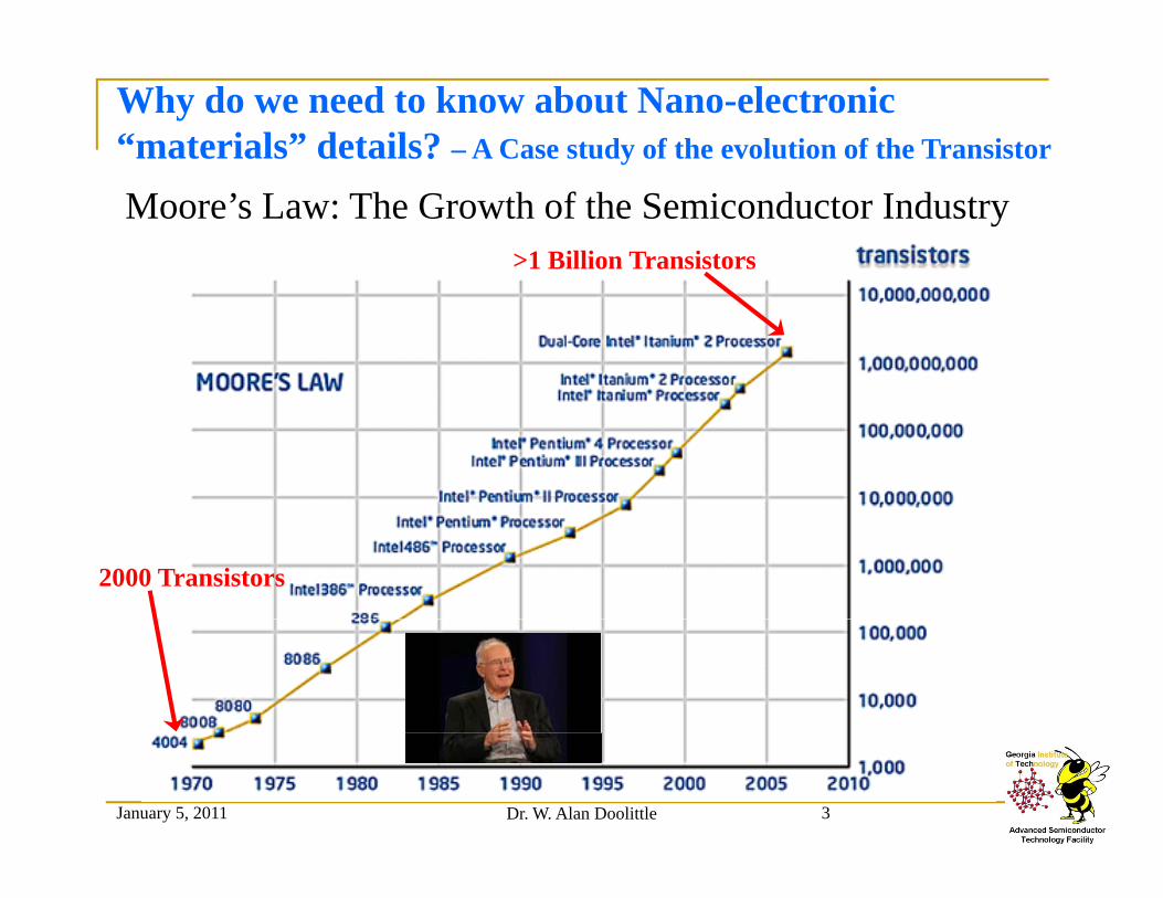
Why do we need to know about Nano-electronic “materials” details? – A Case study of the evolution of the Transistor
Moore’s Law: The Growth of the Semiconductor IndustryyMoore’s law (Gordon Moore, co-founder of Intel, 1965):Empirical rule which predicts that the number of components per chip doubles every 18-24 monthsMoore’s Law turned out to be valid for more than 30 years (and still is!)Moore s Law turned out to be valid for more than 30 years (and still is!)
January 5, 2011 Dr. W. Alan Doolittle 2
Why do we need to know about Nano-electronic “materials” details? – A Case study of the evolution of the Transistor
Moore’s Law: The Growth of the Semiconductor Industry>1 Billion Transistors
2000 Transistors
January 5, 2011 Dr. W. Alan Doolittle 3

Why do we need to know about Nano-electronic “materials” details? – A Case study of the evolution of the Transistor
Transistor functionality scales with transistor count not speed! Speed is less important.p
January 5, 2011 Dr. W. Alan Doolittle 4
from G. Moore, ISSCC 2003
Why do we need to know about Nano-electronic “materials” details? – A Case study of the evolution of the Transistor
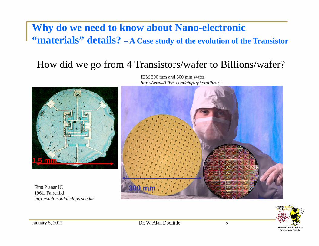
How did we go from 4 Transistors/wafer to Billions/wafer?IBM 200 mm and 300 mm waferIBM 200 mm and 300 mm waferhttp://www-3.ibm.com/chips/photolibrary
1.5 mm
First Planar IC1961, Fairchildhttp://smithsonianchips.si.edu/
300 mm
January 5, 2011 Dr. W. Alan Doolittle 5
p p

Why do we need to know about Nano-electronic “materials” details? – A Case study of the evolution of the Transistor
Sand to Silicon – Major Historical Hurdles.
January 5, 2011 Dr. W. Alan Doolittle 6
Play parts of movie on Silicon Fabrication

Why do we need to know about Nano-electronic “materials” details? – A Case study of the evolution of the Transistor
January 5, 2011 Dr. W. Alan Doolittle 7Slide after Dr. John Cressler

Why do we need to know about Nano-electronic “materials” details? – A Case study of the evolution of the Transistor
Common Statement: First Transistor was invented by Shockley, Brattain and Bardeen on December 23, 1947 at 5 PM – Wrong!
The first patent for the field-effect transistor principle was filed in p p pCanada by Austrian-Hungarian physicist Julius Edgar Lilienfeld on October 22, 1925
The level of understanding you gained about transistors in ECE 3040 is 60 years old!!!!
G T h G d t k th f t h d th d t d t d th t t f
January 5, 2011 Dr. W. Alan Doolittle 8
Ga Tech Graduates make the future happen and thus need to understand the state of the art in order to advance it.
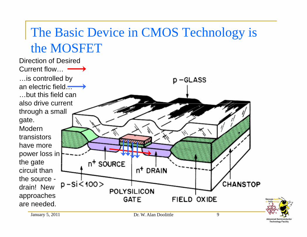
The Basic Device in CMOS Technology is h MOSFETthe MOSFET
Direction of Desired Current flow……is controlled by an electric field……but this field can also drive currentalso drive current through a small gate.Modern transistors have more power loss in the gatethe gate circuit than the source -drain! New
h
January 5, 2011 Dr. W. Alan Doolittle 9
approaches are needed.

Why do we need to know about Nano-electronic “materials” details? – A Case study of the evolution of the Transistor
Early MOSFET: SiO2 Gate Oxide, Aluminum (Al) Source/Drain/Gate metals
Problem: As sizes shrank, devices became unreliable due to metallic spiking through the gate oxide.
Solution: Replace MetalSolution: Replace Metal Gate with a heavily doped poly-silicon.
This change carried us for decades with challenges in fabricationchallenges in fabrication (lithography) being the primary barriers that were overcome …until…
January 5, 2011 Dr. W. Alan Doolittle 10

Why do we need to know about Nano-electronic “materials” details? – A Case study of the evolution of the Transistor
Semi-Modern MOSFET (late 1990’s vintage): SiO2 Gate Oxide, Polysilicon gate metals metal source/drain contacts and Aluminum metal interconnectsgate metals, metal source/drain contacts and Aluminum metal interconnects
Problem: As interconnect sizes shrank, Aluminum lines became too resistive leading to slow RC time constantsSolution: ReplaceSolution: Replace Aluminum with multi-metal contacts (TiN, TaN, etc…) and copper interconnects.
This change carried usThis change carried us for ~ 1 decade with challenges in fabrication (lithography) being the
i b i th t
January 5, 2011 Dr. W. Alan Doolittle 11
primary barriers that were overcome …until…

Why do we need to know about Nano-electronic “materials” details? – A Case study of the evolution of the Transistor
Microprocessor Power ConsumptionG t b thiGates became so thin that the leakage currents through the thin Gate insulator
Gate
consumed more power than the drain-source circuit!
Gate
A new approach is
from G. Moore, ISSCC 2003
A new approach is needed!
January 5, 2011 Dr. W. Alan Doolittle 12

Why do we need to know about Nano-electronic “materials” details? – A Case study of the evolution of the Transistor
from G. Moore, ISSCC 2003
EkD Gate leakage current can be dramatically
Gate
Gateinsulatorinsulator
insulatorinsulator
tVkD
EkD
Gate leakage current can be dramatically lowered by increasing Gate insulator thickness but to do so without changing the channel conductivity, you have to increase the dielectric constant of the insulator.
January 5, 2011 Dr. W. Alan Doolittle 13
GatetLeakageGate eI
the dielectric constant of the insulator. NEW GATE INSULATORS FOR THE FIRST TIME IN 60 YEARS!!!!

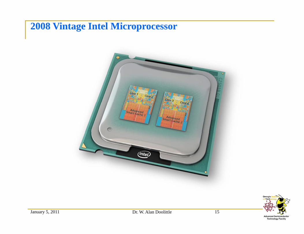
2008 Vintage Intel Microprocessor
January 5, 2011 Dr. W. Alan Doolittle 14
2008 Vintage Intel Microprocessor
January 5, 2011 Dr. W. Alan Doolittle 15

2008 Vintage Intel Microprocessor
January 5, 2011 Dr. W. Alan Doolittle 16

2008 Vintage Intel Microprocessor
January 5, 2011 Dr. W. Alan Doolittle 17

2008 Vintage Intel Microprocessor
4545 nm(~200 atoms)
Hafnium-SilicateSilicate (Oxide)
Strained Si (lower bandgap ( g p
– higher mobility)
January 5, 2011 Dr. W. Alan Doolittle 18

2008 Vintage Intel Microprocessor45 nm45 nm
(~200 atoms)
Hafnium-Silicate•High K Gate Dielectric: Silicate (Oxide)
•High K Gate Dielectric:
•K of SiO2~3.9< Hafnium Silicate ~? < HfO2~ 22
•Deviation from SiO2 required reverting back to Metal Gates (no Poly-silicon)
•Limited Speed of Silicon partially overcome by using SiGe to “mechanically strain” Si channel resulting in E B d difi i h i
Strained Si (lower bandgap
Energy Band structure modification that increases electron/hole mobility.
– higher mobility)
January 5, 2011 Dr. W. Alan Doolittle 19

Strained Silicon MOSFET
Silicon in channel region is strained in two dimensions by placing afrom IEEE Spectrum, 10/2002
Silicon in channel region is strained in two dimensions by placing a Si-Ge layer underneath (or more recently adjacent to) the device layerSt i d Si lt i h i th b d t t f Strained Si results in changes in the energy band structure of conduction and valence band, reducing lattice scattering
Benefit: increased carrier mobility, increased drive current (drain
January 5, 2011 Dr. W. Alan Doolittle 20
current)Slide after Dr. Oliver Brandt

What is in the future? Double-Gate TransistorsGate Transistors
Change of basic transistor structure by introducing a d bl ( ldouble gate (or more general enclose the channel area by the gate)B fi b h l l Benefit: better channel control resulting in better device characteristicsCh ll d bl Challenge: double-gate transistors require completely new device structures with new fabrication challenges
January 5, 2011 Dr. W. Alan Doolittle 21
new fabrication challengesfrom IEEE Spectrum, 10/2002Slide after Dr. Oliver Brandt

Double-Gate Transistor DesignsChannel in chip planeChannel in chip plane
Channel perpendicular to chip plane with current flow i hi l (Fi FET)in chip plane (FinFET)
Channel perpendicular to chip plane with current flow perpendicular to chip plane
January 5, 2011 Dr. W. Alan Doolittle 22
from IEEE Spectrum, 10/2002
Slide after Dr. Oliver Brandt

FinFET Double-Gate Transistor
January 5, 2011 Dr. W. Alan Doolittle 23
from http://www.intel.com/pressroomSlide after Dr. Oliver Brandt

Vertical multi-gate structures take us back to JFET like structures but now with the advantage of insulators. – Life gis circular
January 5, 2011 Dr. W. Alan Doolittle 24

And what about Bipolar and III-V?
January 5, 2011 Dr. W. Alan Doolittle 25
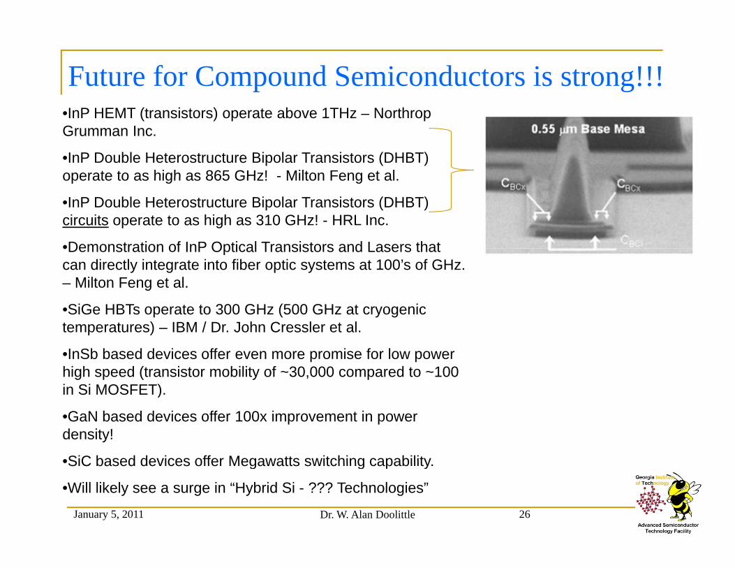
Future for Compound Semiconductors is strong!!!•InP HEMT (transistors) operate above 1THz – Northrop Grumman Inc.
•InP Double Heterostructure Bipolar Transistors (DHBT) operate to as high as 865 GHz! - Milton Feng et aloperate to as high as 865 GHz! - Milton Feng et al.
•InP Double Heterostructure Bipolar Transistors (DHBT) circuits operate to as high as 310 GHz! - HRL Inc.
•Demonstration of InP Optical Transistors and Lasers that•Demonstration of InP Optical Transistors and Lasers that can directly integrate into fiber optic systems at 100’s of GHz. – Milton Feng et al.
•SiGe HBTs operate to 300 GHz (500 GHz at cryogenic temperatures) – IBM / Dr. John Cressler et al.
•InSb based devices offer even more promise for low power high speed (transistor mobility of ~30,000 compared to ~100 in Si MOSFET)in Si MOSFET).
•GaN based devices offer 100x improvement in power density!
•SiC based devices offer Megawatts switching capability
January 5, 2011 Dr. W. Alan Doolittle 26
SiC based devices offer Megawatts switching capability.
•Will likely see a surge in “Hybrid Si - ??? Technologies”

Consider LED as a Case Study of why we must know the materials technologies on the “Nano Scale”the materials technologies on the “Nano Scale”
Movie Complements of Dr. Christian Kisielowski from Lawrence Berkeley DOE Labsfrom Lawrence Berkeley DOE Labs.
January 5, 2011 Dr. W. Alan Doolittle 27
Related Documents